WO2018092830A1 - Dispositif de balayage optique et appareil de formation d'image - Google Patents
Dispositif de balayage optique et appareil de formation d'image Download PDFInfo
- Publication number
- WO2018092830A1 WO2018092830A1 PCT/JP2017/041213 JP2017041213W WO2018092830A1 WO 2018092830 A1 WO2018092830 A1 WO 2018092830A1 JP 2017041213 W JP2017041213 W JP 2017041213W WO 2018092830 A1 WO2018092830 A1 WO 2018092830A1
- Authority
- WO
- WIPO (PCT)
- Prior art keywords
- light source
- straight line
- scanning device
- control substrate
- optical scanning
- Prior art date
- Legal status (The legal status is an assumption and is not a legal conclusion. Google has not performed a legal analysis and makes no representation as to the accuracy of the status listed.)
- Ceased
Links
Images


Classifications
-
- G—PHYSICS
- G03—PHOTOGRAPHY; CINEMATOGRAPHY; ANALOGOUS TECHNIQUES USING WAVES OTHER THAN OPTICAL WAVES; ELECTROGRAPHY; HOLOGRAPHY
- G03G—ELECTROGRAPHY; ELECTROPHOTOGRAPHY; MAGNETOGRAPHY
- G03G15/00—Apparatus for electrographic processes using a charge pattern
- G03G15/04—Apparatus for electrographic processes using a charge pattern for exposing, i.e. imagewise exposure by optically projecting the original image on a photoconductive recording material
- G03G15/04036—Details of illuminating systems, e.g. lamps, reflectors
- G03G15/04045—Details of illuminating systems, e.g. lamps, reflectors for exposing image information provided otherwise than by directly projecting the original image onto the photoconductive recording material, e.g. digital copiers
- G03G15/04072—Details of illuminating systems, e.g. lamps, reflectors for exposing image information provided otherwise than by directly projecting the original image onto the photoconductive recording material, e.g. digital copiers by laser
-
- B—PERFORMING OPERATIONS; TRANSPORTING
- B41—PRINTING; LINING MACHINES; TYPEWRITERS; STAMPS
- B41J—TYPEWRITERS; SELECTIVE PRINTING MECHANISMS, i.e. MECHANISMS PRINTING OTHERWISE THAN FROM A FORME; CORRECTION OF TYPOGRAPHICAL ERRORS
- B41J2/00—Typewriters or selective printing mechanisms characterised by the printing or marking process for which they are designed
- B41J2/435—Typewriters or selective printing mechanisms characterised by the printing or marking process for which they are designed characterised by selective application of radiation to a printing material or impression-transfer material
- B41J2/47—Typewriters or selective printing mechanisms characterised by the printing or marking process for which they are designed characterised by selective application of radiation to a printing material or impression-transfer material using the combination of scanning and modulation of light
-
- G—PHYSICS
- G02—OPTICS
- G02B—OPTICAL ELEMENTS, SYSTEMS OR APPARATUS
- G02B26/00—Optical devices or arrangements for the control of light using movable or deformable optical elements
- G02B26/08—Optical devices or arrangements for the control of light using movable or deformable optical elements for controlling the direction of light
- G02B26/10—Scanning systems
- G02B26/12—Scanning systems using multifaceted mirrors
- G02B26/121—Mechanical drive devices for polygonal mirrors
- G02B26/122—Control of the scanning speed of the polygonal mirror
-
- G—PHYSICS
- G02—OPTICS
- G02B—OPTICAL ELEMENTS, SYSTEMS OR APPARATUS
- G02B26/00—Optical devices or arrangements for the control of light using movable or deformable optical elements
- G02B26/08—Optical devices or arrangements for the control of light using movable or deformable optical elements for controlling the direction of light
- G02B26/10—Scanning systems
- G02B26/12—Scanning systems using multifaceted mirrors
- G02B26/127—Adaptive control of the scanning light beam, e.g. using the feedback from one or more detectors
-
- G—PHYSICS
- G02—OPTICS
- G02B—OPTICAL ELEMENTS, SYSTEMS OR APPARATUS
- G02B5/00—Optical elements other than lenses
- G02B5/08—Mirrors
- G02B5/09—Multifaceted or polygonal mirrors, e.g. polygonal scanning mirrors; Fresnel mirrors
-
- G—PHYSICS
- G03—PHOTOGRAPHY; CINEMATOGRAPHY; ANALOGOUS TECHNIQUES USING WAVES OTHER THAN OPTICAL WAVES; ELECTROGRAPHY; HOLOGRAPHY
- G03G—ELECTROGRAPHY; ELECTROPHOTOGRAPHY; MAGNETOGRAPHY
- G03G15/00—Apparatus for electrographic processes using a charge pattern
- G03G15/04—Apparatus for electrographic processes using a charge pattern for exposing, i.e. imagewise exposure by optically projecting the original image on a photoconductive recording material
- G03G15/043—Apparatus for electrographic processes using a charge pattern for exposing, i.e. imagewise exposure by optically projecting the original image on a photoconductive recording material with means for controlling illumination or exposure
-
- H—ELECTRICITY
- H04—ELECTRIC COMMUNICATION TECHNIQUE
- H04N—PICTORIAL COMMUNICATION, e.g. TELEVISION
- H04N1/00—Scanning, transmission or reproduction of documents or the like, e.g. facsimile transmission; Details thereof
- H04N1/04—Scanning arrangements, i.e. arrangements for the displacement of active reading or reproducing elements relative to the original or reproducing medium, or vice versa
- H04N1/113—Scanning arrangements, i.e. arrangements for the displacement of active reading or reproducing elements relative to the original or reproducing medium, or vice versa using oscillating or rotating mirrors
-
- G—PHYSICS
- G03—PHOTOGRAPHY; CINEMATOGRAPHY; ANALOGOUS TECHNIQUES USING WAVES OTHER THAN OPTICAL WAVES; ELECTROGRAPHY; HOLOGRAPHY
- G03G—ELECTROGRAPHY; ELECTROPHOTOGRAPHY; MAGNETOGRAPHY
- G03G15/00—Apparatus for electrographic processes using a charge pattern
- G03G15/55—Self-diagnostics; Malfunction or lifetime display
Definitions
- the present invention relates to an optical scanning device used in an image forming apparatus such as a copying machine, a printer, and a facsimile machine.
- An optical scanning device used in an image forming apparatus such as a copying machine, a printer, or a facsimile machine performs light modulation on a laser beam emitted from a light source according to an image signal, and a light beam which is light modulated.
- Deflection scanning is performed with a deflector.
- the deflected laser beam is imaged on the surface of the photosensitive drum by a scanning lens such as an f ⁇ lens to form an electrostatic latent image.
- the developing agent supplies a developer to the electrostatic latent image formed on the surface of the photosensitive drum to develop it as a toner image to develop the image, which is transferred onto a recording material such as paper and sent to a fixing device.
- Printing is performed by heating and fixing the toner image on the recording material.
- the laser light flux emitted from the light source is subjected to deflection scanning with a light deflector comprising a rotary polygon mirror.
- a control substrate is mounted on which a BD (Beam Detect) sensor for receiving a laser beam and generating a horizontal synchronization signal is mounted.
- the control board is connected to the light source.
- the control substrate is fixed to the outer wall of the optical box of the optical scanning device by screws.
- Patent Documents 1 and 2 have the following problems.
- the electronic components on the control substrate are reflowed (soldered).
- the reflow soldering is to heat, melt and solder the solder which has been previously applied at normal temperature.
- the heat at the time of the reflow soldering may cause warpage in the control substrate.
- the control substrate may be warped depending on the seating surface accuracy of the fixed seating surface.
- the control substrate on which the BD sensor is mounted is fixed to the optical box by screws.
- the fixed point is located away from the BD sensor, and the position of the BD sensor is shifted in the warp direction due to the influence of the warp of the control substrate.
- the timing of generating a horizontal synchronization signal for controlling the image writing position may shift due to the effect of the warp.
- the present invention solves the above-mentioned problems, and an object of the present invention is to form an image with a stable image writing position by reliably and accurately positioning detection means for generating a horizontal synchronization signal on an optical box.
- an optical scanning device capable of
- a typical configuration of an optical scanning device comprises: a light source; a deflector having a rotary polygon mirror for deflecting and scanning a light beam emitted from the light source;
- the detection means comprises: detection means for detecting the write-out position of the light beam reflected by the mirror, a control substrate electrically connected to the light source, and an optical box for accommodating the deflector.
- the control substrate is fixed to the control board, and the control substrate is fixed to the optical box by fixing means, and at least one of the fixing means is relative to a first straight line connecting the light source and the detection means. It is characterized in that it is disposed on a second straight line orthogonal to and passing through the detection means fixed to the control substrate.
- the detection means for generating the horizontal synchronization signal can be accurately and accurately positioned on the optical box, and an image having a stable image writing position can be formed.
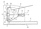
- FIG. 1 is a cross-sectional explanatory view showing the configuration of an image forming apparatus provided with an optical scanning device according to the present invention. It is a perspective view showing the composition of the optical scanning device concerning the present invention. It is side explanatory drawing which shows the positional relationship of the control board in 1st Embodiment, BD sensor, and fixing screw. It is a disassembled perspective view which shows the positional relationship of the control board in 1st Embodiment, an optical box, and fixing screw.
- FIG. 5 is a cross-sectional view taken along the line BB in FIG. 3 showing the positional relationship between the light receiving surface of the BD sensor and the control substrate in the first embodiment.
- FIG. 4 is a cross-sectional view taken along the line BB in FIG. 3 showing the positional relationship between the light receiving surface of the BD sensor and the laser beam incident on the light receiving surface.
- FIG. 1 is a cross-sectional explanatory view showing the configuration of an image forming apparatus provided with an optical scanning device 101 according to the present invention.
- An image forming apparatus 110 shown in FIG. 1 is an example of an electrophotographic laser printer.
- An image forming apparatus 110 shown in FIG. 1 includes an optical scanning device 101.
- the image forming apparatus 110 includes an image forming unit that forms an image on the recording material P based on the image exposed and scanned on the surface of the photosensitive drum 103 serving as an image carrier by the optical scanning device 101.
- the laser light flux L (light flux) emitted from the optical scanning device 101 is scan-exposed on the surface of the photosensitive drum 103 to form an electrostatic latent image.
- An image forming apparatus 110 shown in FIG. 1 emits a laser beam L based on the obtained image information by an optical scanning device 101 as an exposure unit, and a photosensitive drum 103 as an image carrier incorporated in the process cartridge 102. Irradiate on the surface.
- the process cartridge 102 is integrally provided with a photosensitive drum 103, a charging roller 15 serving as a charging unit as an image forming process unit acting on the photosensitive drum 103, a developing device 16 serving as a developing unit, and a cleaner 25 serving as a cleaning unit. It is done.
- the process cartridge 102 is detachably provided to the main body of the image forming apparatus 110.
- the surface of the photosensitive drum 103 as an image carrier rotating in the clockwise direction in FIG. 1 is uniformly charged by the charging roller 15 as a charging unit.
- the laser beam L according to the image information is exposed and scanned by the optical scanning device 101 on the surface of the uniformly charged photosensitive drum 103.
- an electrostatic latent image corresponding to the image information is formed on the surface of the photosensitive drum 103.
- the electrostatic latent image formed on the surface of the photosensitive drum 103 is supplied with a developer by a developing roller 16a serving as a developer carrying member provided in a developing device 16 serving as a developing unit, and is developed as a toner image.
- the recording material P accommodated in the feeding cassette 104 is fed out by the feeding roller 105 and separated and fed one by one in cooperation with the separation roller 17. Further, the leading end portion is in contact with the nip portion of the registration roller 18 which is nipped and conveyed by the conveyance roller 106 and stopped. The skew of the recording material P is corrected by being handled by the stiffness of the recording material P.
- the registration roller 18 rotates in synchronization with the timing when the toner image formed on the surface of the photosensitive drum 103 reaches the transfer nip N formed by the surface of the photosensitive drum 103 and the transfer roller 107 serving as the transfer means. .
- the recording material P is nipped by the registration roller 18 and conveyed to the transfer nip N.
- a transfer bias is applied to the transfer roller 107 by a transfer bias power supply (not shown), and the toner image formed on the surface of the photosensitive drum 103 is transferred onto the recording material P.
- the residual toner remaining on the surface of the photosensitive drum 103 after transfer is removed by the cleaner 25 and collected.
- the recording material P on which an unfixed toner image is formed is nipped by the photosensitive drum 103 and the transfer roller 107 and conveyed to a fixing device 108 serving as a fixing unit.
- a fixing device 108 serving as a fixing unit.
- the toner image is thermally fused by being heated and pressurized, and the toner image is thermally fixed on the recording material P.
- the recording material P nipped and conveyed by the fixing roller and the pressure roller of the fixing device 108 is discharged by the discharge roller 109 onto the discharge tray 19 provided outside the apparatus.
- the charging roller 15 serving as a charging unit serving as an image forming process unit acting on the photosensitive drum 103 and the developing device 16 serving as a developing unit are provided integrally with the photosensitive drum 103 inside the process cartridge 102.
- each image forming process unit can be configured separately from the photosensitive drum 103.
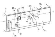
- FIG. 2 is a perspective view showing the configuration of the optical scanning device 101 according to the present invention.
- a semiconductor laser unit 1 is a light source for emitting a laser beam L.
- the anamorphic collimator lens 2 is formed by integrating a collimator lens and a cylindrical lens.
- the aperture 3 is an optical stop that shapes the laser beam L into a predetermined shape.
- the deflector 5 rotationally drives the rotary polygon mirror 4.
- the deflector 5 includes a rotary polygon mirror 4 for deflecting the laser light flux L (light flux) emitted from the semiconductor laser unit 1 (light source).
- the BD (Beam Detect) sensor 6 is a detection unit that detects a writing position of the laser light flux L (light flux) reflected by the rotary polygon mirror 4.
- the control substrate 7 is electrically connected to the semiconductor laser unit 1 (light source).
- the signal transmission connector 8 is provided on the control board 7.
- the f ⁇ lens 9 is a scanning lens.
- the f ⁇ lens 9 has a lens characteristic (f ⁇ characteristic) that forms an image of a size (f ⁇ ⁇ ) obtained by multiplying the focal length f of the f ⁇ lens 9 when the laser beam L enters at an angle ⁇ . Have.
- the optical box 10 accommodates a semiconductor laser unit 1 (light source), an anamorphic collimator lens 2, an aperture 3, a rotating polygon mirror 4, a deflector 5 for rotating the rotating polygon mirror 4, an f ⁇ lens 9 and the like.
- An opening 10 c provided at the upper portion of the optical box 10 is covered by a lid 26 shown in FIG.
- the fixing screws 11a to 11c are fixing means for fixing the control substrate 7 to the fixed bearing surfaces 13a to 13c provided on the outer surface of the side wall 10a of the optical box 10.
- the laser beam L is emitted from the semiconductor laser unit 1 according to an image signal received through the signal transmission connector 8 provided on the control substrate 7.
- the laser beam L is converted by the anamorphic lens 2 into parallel light or weakly convergent light in the main scanning direction (axial direction of the photosensitive drum 103). Further, it is converted into convergent light in the sub scanning direction (the circumferential direction of the photosensitive drum 103).
- the laser beam L is shaped into a predetermined shape by the aperture 3 formed of a through hole, and is connected in a focal line shape extending in the main scanning direction (axial direction of the photosensitive drum 103) on the reflecting surface 4a of the rotating polygon mirror 4.
- Image The laser beam L formed on the reflecting surface 4a of the rotary polygon mirror 4 is deflected by rotating the rotary polygon mirror 4 in the direction of arrow A in FIG.
- the laser beam L deflected by the rotary polygon mirror 4 is incident on the light receiving surface 61 of the BD sensor 6 mounted on the control substrate 7.
- the BD sensor 6 detects the writing position of the laser beam L in the main scanning direction, and outputs a BD (Beam Detect) signal according to the detected timing.
- the BD signal is a trigger signal of control for aligning the writing position in the main scanning direction.
- the laser beam L deflected and scanned by the rotary polygon mirror 4 enters the f ⁇ lens 9.
- the f ⁇ lens 9 is designed to condense the laser beam L so as to form a spot on the surface of the photosensitive drum 103 so that the scanning speed of the spot is kept constant.
- the f ⁇ lens 9 is formed of an aspheric lens.
- the laser beam L that has passed through the f ⁇ lens 9 is emitted from the opening 10 b of the optical box 10 and is imaged and scanned on the surface of the photosensitive drum 103.
- the control board 7 is fixed to the outer surface of the side wall 10 a of the optical box 10 using fixing screws 11 a, 11 b and 11 c.
- the opening 10c at the top of the optical box 10 is covered by a lid 26 shown in FIG.
- the rotary polygon mirror 4 deflects the laser beam L by rotating in the direction of arrow A in FIG. 2, and the laser beam L is deflected in the main scanning direction on the surface of the photosensitive drum 103 uniformly charged by the charging roller 15.
- the surface of the photosensitive drum 103 is exposed by scanning in the axial direction of the drum 103). Further, exposure in the sub scanning direction (the circumferential direction of the photosensitive drum 103) is performed by rotationally driving the photosensitive drum 103 in the clockwise direction in FIG. Thereby, an electrostatic latent image corresponding to the image information is formed on the surface of the photosensitive drum 103.
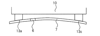
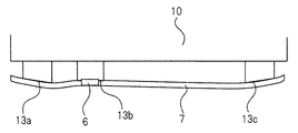
- FIG. 3 is an explanatory side view showing the positional relationship between the control board 7, the BD sensor 6 and the fixing screws 11a to 11c in the present embodiment.
- FIG. 4 is an exploded perspective view showing the positional relationship among the control board 7, the optical box 10, and the fixing screws 11a to 11c in the present embodiment.
- the control substrate 7 shown in FIGS. 3 and 4 is formed of a single-sided substrate made of paper phenolic resin.
- the paper phenolic resin substrate is formed by impregnating a paper with an insulating material with a phenolic resin, and is also called a bakelite substrate.
- the control substrate 7 of a single-sided substrate is used, but the control substrate 7 of a double-sided substrate may be used.
- control board 7 As a material of the control board 7, it is also possible to adopt glass epoxy resin. In the present embodiment, cost reduction can be achieved by employing paper phenol resin as the material of the control substrate 7. Although the control substrate 7 made of paper phenolic resin is cheaper than the control substrate 7 made of glass epoxy, its mechanical strength is low and warpage tends to occur.
- a laser driver (not shown) is mounted along with the BD sensor 6 on the mounting surface of the control board 7 on which the electronic component is mounted. These electronic components are soldered and fixed to the control substrate 7 by reflow soldering. The reflow soldering is to heat, melt and solder the solder which has been previously applied at normal temperature.
- the semiconductor laser unit 1 employs a two-beam laser emitted from each of two light emitting points. As shown in FIG. 4, the four terminals 1a, 1b, 1c, 1d of the semiconductor laser unit 1 are inserted through the through holes 7a, 7b, 7c, 7d provided in the control substrate 7, and the control substrate 7 shown in FIG. Are electrically connected by solder at four points of the electric circuit provided in the connection region 12 of FIG. In FIG. 3, the connection region 12 indicated by a broken line corresponds to a circle obtained by projecting the outer diameter of the cylindrical exterior of the semiconductor laser unit 1 (light source) shown in FIG.
- the control board 7 is provided with through holes 14a, 14b, provided in the control board 7 with respect to the fixed bearing surfaces 13a, 13b, 13c provided on the outer surface of the side wall 10a of the optical box 10. It is fixed at three points by fixing screws 11a to 11c inserted into 14c.
- the fixing screws 11a and 11c are provided in the vicinity of a straight line C passing through the center position 6a of the BD sensor 6 in parallel with the opening 10c surface of the optical box 10 shown in FIG. It is disposed on a straight line M passing through the center position 6 a of the BD sensor 6.
- the straight line C shown in FIG. 3 is also a straight line connecting the center position 6 a of the BD sensor 6 and the center position 12 a of the connection region 12 of the semiconductor laser unit 1.
- the fixing screw 11b which is at least one of the three fixing screws 11a to 11c (fixing means) is disposed at the following position.
- FIG. 4 shows fixed bearing surfaces 13a to 13c for fixing the control substrate 7 to the outer surface of the side wall 10a of the optical box 10.
- fixed bearing surfaces 13a to 13c are provided on the outer surface of the side wall 10a of the optical box 10.
- the surfaces on which the fixed bearing surfaces 13a to 13c abut the back surface of the control board 7 are flat.
- Female screw holes 13a1, 13b1 and 13c1 are formed at the centers of the fixed bearing surfaces 13a to 13c.
- the fixing screws 11a to 11c inserted into the through holes 14a to 14c of the control board 7 are male screw portions 11a1 to 11c1 formed on the shaft portions of the fixing screws 11a to 11c as female screw holes of the fixing bearing surfaces 13a to 13c. Screw on 13a1 to 13c1. As a result, the control board 7 is fixed on the fixing seat surfaces 13a to 13c by the fixing screws 11a to 11c.
- the laser beam L deflected and scanned by the rotary polygon mirror 4 passes through the through hole 10 a 1 penetrating the side wall 10 a of the optical box 10 and the through hole 7 e penetrating the control substrate 7. Then, the light receiving surface 61 is disposed in the through hole 7 e of the control substrate 7 and is incident on the light receiving surface 61 of the BD sensor 6 mounted on the control substrate 7.
- FIG. 5 is a cross-sectional view taken along the line BB in FIG. 3 showing the positional relationship between the light receiving surface 61 of the BD sensor 6 and the control substrate 7 in the present embodiment.
- the BD sensor 6 shown in FIG. 5 generates a BD (Beam Detect) signal when the laser light flux L is incident on the light receiving surface 61 of the BD sensor 6.
- a BD (Beam Detect) signal generated by the BD sensor 6 is transmitted to the control substrate 7 via the terminal 62.
- the light receiving surface 61 of the BD sensor 6 is disposed substantially the same as the back surface 7 f of the control substrate 7 facing the outer surface of the side wall 10 a of the optical box 10.
- the BD sensor 6 outputs a BD (Beam Detect) signal and is transmitted to the control substrate 7 through the terminal 62.
- the BD sensor 6 is shown schematically in FIGS. 6A to 6D because it is hidden by the control substrate 7.
- the optical box 10 is produced by injection molding of a resin.
- the fixed bearing surfaces 13a and 13c may have an inclination due to variations in manufacturing.
- the warpage of the control board 7 is classified into four types as shown in FIGS. 6A to 6D according to the inclination states of the fixed bearing surfaces 13a and 13c shown in FIGS. 6A to 6D.
- the warpage of the control substrate 7 is convex to the outside at the place where the BD sensor 6 is provided. It will be in the state away from the outer surface of the side wall 10a. Further, in the inclined state of the fixed bearing surfaces 13a and 13c shown in FIG. 6B and FIG. 6D, the warpage of the control substrate 7 is convex inward at the location where the BD sensor 6 is provided. The outer surface of the side wall 10a of 10 is approached.
- the optical path length of the laser light flux L incident on the light receiving surface 61 of the BD sensor 6 is longer than the normal optical path length. Further, in the case of FIG. 6B and FIG. 6D, the optical path length of the laser light flux L incident on the light receiving surface 61 of the BD sensor 6 is shorter than the normal optical path length.
- FIG. 7A is a cross-sectional view taken along the line BB in FIG. 3 showing the positional relationship between the light receiving surface 61 of the BD sensor 6 and the laser light flux L incident on the light receiving surface 61.
- the laser beam L is incident on the light receiving surface 61 of the BD sensor 6 at an incident angle ⁇ with respect to the normal direction (vertical direction) of the light receiving surface 61 at an angle larger than 0 °. It is set.
- the reason for setting such an incident angle ⁇ is that, when the normal direction of the light receiving surface 61 of the BD sensor 6 matches the incident direction of the laser beam L, part of the laser beam L on the surface of the BD sensor 6 It is reflected. The reflected light returns to the semiconductor laser unit 1 which is a light source, and return light noise is generated. The return light noise makes the laser oscillation unstable. This is to prevent this.
- FIGS. 6A to 6D when the position of the light receiving surface 61 of the BD sensor 6 deviates from the normal position due to the inclination of the fixed bearing surfaces 13a and 13c and the warp of the control substrate 7, FIG. This will be described using FIG. 7C.
- FIGS. 7B and 7C show the case where the position of the light receiving surface 61 of the BD sensor 6 is moved from the normal position due to the inclination of the fixed bearing surfaces 13a and 13c and the warpage of the control substrate 7 It is a figure which shows positional relationship.
- FIG. 7B shows a case where the position of the light receiving surface 61 of the BD sensor 6 deviates from the normal position on the extension of the laser beam L in the optical axis direction.
- the timing at which the laser beam L enters the light receiving surface 61 of the BD sensor 6 does not change. For this reason, there is no shift in the writing position.
- FIG. 7C shows a case where the position of the light receiving surface 61 of the BD sensor 6 deviates from the normal position to a position deviated from the optical axis direction of the laser beam L.
- the timing at which the laser beam L is incident on the light receiving surface 61 of the BD sensor 6 is not the laser beam L at the regular position but the laser deviated from the optical axis direction of the laser beam L by an angle ⁇ 2.
- the luminous flux L 2 is incident on the light receiving surface 61 of the BD sensor 6.
- the detection timing of the laser beam L2 incident on the light receiving surface 61 of the BD sensor 6 is advanced by the angle ⁇ 2. As a result, a shift in the writing position occurs.
- the writing position on the image shifts.
- the margin on the image printed on the recording material P is shifted.
- FIG. 7C when the laser beam L at the regular position deviates from the optical axis direction of the laser beam L to the upstream side in the scanning direction of the laser beam L by the angle ⁇ 2, the image writing timing is advanced, and printing on the recording material P is performed. The margin on the image is smaller on the writing side.
- FIG. 8A and 8B show the BD sensor 6 and the optical box when the control substrate 7 in the warped state shown in FIG. 6A is further fixed to the fixed seat 13b provided on the outer surface of the side wall 10a of the optical box 10.
- 10 is a cross-sectional explanatory view showing a positional relationship with 10;
- FIG. 8A shows the case where the fixed bearing surface 13b is not inclined.
- FIG. 8B shows the case where the fixed seating surface 13b is inclined.
- the fixed bearing surface 13b and the BD sensor 6 are disposed on the same plane (on the straight line M in FIG. 3) orthogonal to the scanning direction of the laser beam L (in the direction of arrow A in FIG. 2).
- the control substrate 7 is further fixed by the fixed bearing surface 13b.
- the position of the BD sensor 6 is fixed at the position on the straight line M in FIG. 3 where the fixed seating surface 13b is disposed without being affected by the warpage of the control substrate 7 even if the control board 7 is warped.
- the light receiving surface 61 of the BD sensor 6 is disposed substantially flush with the back surface 7f of the control substrate 7.
- the position at which the laser beam L is received on the light receiving surface 61 hardly changes.
- the displacement of the position of the BD sensor 6 which generates the horizontal synchronization signal due to the influence of the warpage of the control substrate 7 is suppressed, and the timing of generating the horizontal synchronization signal for controlling the image writing position is prevented from being displaced.
- FIG. 9 is a perspective view showing the positional relationship among the semiconductor laser unit 1 in the second embodiment, the connection area 20 for fixing the semiconductor laser unit 1 on the control substrate 21, the signal transmission connector 23, and the fixing screw 22.
- FIG. 9 is a perspective view showing the positional relationship among the semiconductor laser unit 1 in the second embodiment, the connection area 20 for fixing the semiconductor laser unit 1 on the control substrate 21, the signal transmission connector 23, and the fixing screw 22.
- the control board 7 is fixed to the outer surface of the side wall 10a of the optical box 10 by three fixing screws 11a to 11c.
- the signal transmission connector 8 is an example in which the longitudinal direction is provided laterally below the fixing screw 11 c.
- the control substrate 7 is fixed to the outer surface of the side wall 10 a of the optical box 10 by one fixing screw 22.
- the signal transmission connector 23 is an example provided on the left side of the fixing screw 22 and in the longitudinal direction in the longitudinal direction. The positional relationship between the signal transmission connector 23, the BD (Beam Detect) sensor 24 and the fixing screw 22 of the second embodiment will be described with reference to FIG.
- connection region 20 constitutes a first connection portion in which the semiconductor laser unit 1 (light source) is connected to the control substrate 21.
- control board 7 is fixed to the fixing seat surfaces 13a to 13c provided on the outer surface of the side wall 10a of the optical box 10 using the three fixing screws 11a to 11c.
- control board 21 is fixed to a not-shown fixing seat provided on the outer surface of the side wall 10a of the optical box 10 using one fixing screw 22 for cost reduction.
- the fixing screw 22 of the second embodiment is disposed at a position corresponding to the fixing screw 11b of the first embodiment shown in FIG.
- one fixing screw 22 (fixing means) is disposed at the following position.
- a straight line M which is orthogonal to a straight line C (first straight line) connecting the semiconductor laser unit 1 (light source) and the BD sensor 24 (detection means) and passes through the BD sensor 24 (detection means) fixed to the control substrate 21 It is arranged at the top (on the second straight line).
- the signal transmission connector 23 shown in FIG. 9 constitutes a second connection portion in which the control board 21 is electrically connected to the outside.
- the signal transmission connector 23 (second connection portion) is closer to the BD sensor 24 side than the straight line E (fourth straight line) orthogonal to the straight line C (first straight line) and passing through the semiconductor laser unit 1 (light source) Is disposed on the detection means side).
- the signal transmission connector 23 is electrically connected to the outside using a bundle (not shown). When the bundle of wires detachably connected to the signal transmission connector 23 is inserted and removed, a force is applied to the control substrate 21 and the control substrate 21 is deformed.
- the four terminals 1a to 1d of the semiconductor laser unit 1 are inserted into the through holes 21a to 21d provided in the control substrate 21 as shown in FIG. 4 and described above. Then, solder is electrically conducted and connected at four places of the electric circuit provided in the connection area 20 of the control substrate 21 shown in FIG.
- control substrate 21 and the semiconductor laser unit 1 are fixed by solder, and when the control substrate 21 is deformed, the force is applied to the solder of the connection region 20 as well.
- peeling may occur on the connection surface of the control substrate 21 with the electric circuit.
- the fixing screw 22 (fixed) is provided between the connection region 20 (first connection portion) and the signal transmission connector 23 (second connection portion) in order to reduce the influence of the force of the connection region 20 on the solder. Means).
- the deformation of the control substrate 21 due to the insertion and removal of the bundle of signal transmission connectors 23 does not easily spread to the solder of the connection area 20 of the semiconductor laser unit 1.
- the laser beam L deflected and scanned by the rotary polygon mirror 4 passes through the through hole 10a1 passing through the side wall 10a of the optical box 10 and the through hole 21e passing through the control substrate 21. Then, the light receiving surface 61 is disposed in the through hole 21 e of the control substrate 21 and the light receiving surface 61 of the BD sensor 24 mounted on the control substrate 21 is incident.
- the horizontal synchronization signal for controlling the image writing position can be suppressed with a configuration cheaper than the first embodiment, suppressing the displacement of the position of the BD sensor 24 due to the influence of the warpage of the control substrate 21. It can suppress that the timing which generate
- FIG. 10 is a perspective explanatory view showing another configuration of the second embodiment.
- the control substrate 21 is fixed to the side wall 10a of the optical box 10 by a fixing screw 22 as one fixing means.
- the fixing screw 22 is disposed on a straight line M (second straight line) orthogonal to a straight line C (first straight line) connecting the semiconductor laser unit 1 (light source) and the BD sensor 24 (detection means).
- a straight line D (third straight line) parallel to the straight line M (second straight line) passing through the end 20 a of the semiconductor laser unit 1 (light source) on the BD sensor 24 side (detecting means side) is considered.
- the fixing screw 22 (fixing means) is disposed closer to the BD sensor 24 (detecting means) than the straight line D.
- the fixing screw 22 (fixing means) is disposed between the signal transmission connector 23 and the BD sensor 24 (detection means) to which the control substrate 21 is electrically connected to the outside.
- the fixing screw 22 (fixing means) is disposed closer to the BD sensor 24 than the signal transmission connector 23.
- the fixing screw 22 (fixing means) is provided at a position farther from the BD sensor 24 (detecting means) than the semiconductor laser unit 1 (light source), but the position is as shown in FIG. It is not limited.
- a straight line M (second straight line) orthogonal to a straight line C (first straight line) connecting the semiconductor laser unit 1 (light source) and the BD sensor 24 (detection means)
- a straight line G (fifth straight line) passing parallel to the straight line M and passing through the end 24 b of the BD sensor 24 (detection means) farthest from the semiconductor laser unit 1 (light source)
- the fixing screw 22 (fixing means) may be disposed on the straight line G.
- the connection area 20 indicated by a broken line corresponds to a circle obtained by projecting the outer diameter of the cylindrical exterior of the semiconductor laser unit 1 (light source) onto the control substrate 21.
- the other configuration is the same as that of the first embodiment, and the same effect can be obtained.
- FIG. 12 is a perspective view showing another configuration of the third embodiment.
- the control substrate 21 is fixed to the side wall 10 a of the optical box 10 by a fixing screw 22 as one fixing means.
- the fixing screw 22 is disposed on a straight line M (second straight line) orthogonal to a straight line C (first straight line) connecting the semiconductor laser unit 1 (light source) and the BD sensor 24 (detection means). .
- the fixing screw 22 (fixing means) is disposed closer to the BD sensor 24 (detecting means) than the semiconductor laser unit 1 (light source).
- the connection region 20 indicated by a broken line corresponds to a circle obtained by projecting the outer diameter of the cylindrical exterior of the semiconductor laser unit 1 (light source) onto the control substrate 21.
- the other configuration is the same as that of the first and second embodiments, and the same effect can be obtained.
Landscapes
- Physics & Mathematics (AREA)
- General Physics & Mathematics (AREA)
- Optics & Photonics (AREA)
- Engineering & Computer Science (AREA)
- Multimedia (AREA)
- Signal Processing (AREA)
- Facsimile Scanning Arrangements (AREA)
- Mechanical Optical Scanning Systems (AREA)
- Laser Beam Printer (AREA)
Abstract
La présente invention concerne un dispositif de balayage optique capable de positionner de manière fiable et très précise un moyen de détection pour générer un signal de synchronisation horizontale dans une boîte optique, et former des images dont les positions de début d'écriture d'image sont stables. Ce dispositif de balayage optique est caractérisé en ce qu'un capteur BD (6) pour détecter une position de début d'écriture d'un flux de faisceau laser est fixé à une carte de commande (7) connecté électriquement à une unité laser à semi-conducteur (1), la carte de commande (7) étant fixée à un boîtier optique logeant un déflecteur pourvu d'un miroir polygonal rotatif par fixation de vis (11a-11c), et la vis de fixation (11b) s'intersecte à un angle droit avec une première ligne droite (C) reliant l'unité laser à semi-conducteur (1) et le capteur BD (6) et est disposé plus près du capteur BD (6) qu'une ligne droite passant au-dessus de l'unité laser à semi-conducteur (1).
Priority Applications (2)
| Application Number | Priority Date | Filing Date | Title |
|---|---|---|---|
| CN201780070279.2A CN109964164B (zh) | 2016-11-17 | 2017-11-16 | 光学扫描装置和图像形成装置 |
| US16/411,578 US10698335B2 (en) | 2016-11-17 | 2019-05-14 | Optical scanning apparatus and image forming apparatus |
Applications Claiming Priority (4)
| Application Number | Priority Date | Filing Date | Title |
|---|---|---|---|
| JP2016223899 | 2016-11-17 | ||
| JP2016-223899 | 2016-11-17 | ||
| JP2017213548A JP6526150B2 (ja) | 2016-11-17 | 2017-11-06 | 光学走査装置及び画像形成装置 |
| JP2017-213548 | 2017-11-06 |
Related Child Applications (1)
| Application Number | Title | Priority Date | Filing Date |
|---|---|---|---|
| US16/411,578 Continuation US10698335B2 (en) | 2016-11-17 | 2019-05-14 | Optical scanning apparatus and image forming apparatus |
Publications (1)
| Publication Number | Publication Date |
|---|---|
| WO2018092830A1 true WO2018092830A1 (fr) | 2018-05-24 |
Family
ID=62145503
Family Applications (1)
| Application Number | Title | Priority Date | Filing Date |
|---|---|---|---|
| PCT/JP2017/041213 Ceased WO2018092830A1 (fr) | 2016-11-17 | 2017-11-16 | Dispositif de balayage optique et appareil de formation d'image |
Country Status (2)
| Country | Link |
|---|---|
| CN (1) | CN109964164B (fr) |
| WO (1) | WO2018092830A1 (fr) |
Families Citing this family (1)
| Publication number | Priority date | Publication date | Assignee | Title |
|---|---|---|---|---|
| JP7449158B2 (ja) * | 2020-04-30 | 2024-03-13 | キヤノン株式会社 | 画像形成装置 |
Citations (5)
| Publication number | Priority date | Publication date | Assignee | Title |
|---|---|---|---|---|
| JP2004240275A (ja) * | 2003-02-07 | 2004-08-26 | Pentax Corp | レーザ走査装置 |
| JP2006065012A (ja) * | 2004-08-27 | 2006-03-09 | Pentax Corp | レーザ走査装置 |
| US20130033557A1 (en) * | 2011-08-03 | 2013-02-07 | Samsung Electronics Co., Ltd | Light scanning unit and image forming apparatus employing the same |
| JP2013238701A (ja) * | 2012-05-14 | 2013-11-28 | Ricoh Co Ltd | 光走査装置及び画像形成装置 |
| JP2015011160A (ja) * | 2013-06-28 | 2015-01-19 | キヤノン株式会社 | 画像形成装置 |
Family Cites Families (13)
| Publication number | Priority date | Publication date | Assignee | Title |
|---|---|---|---|---|
| JP3291906B2 (ja) * | 1994-04-11 | 2002-06-17 | キヤノン株式会社 | 走査光学装置 |
| US6677974B2 (en) * | 2001-03-21 | 2004-01-13 | Kabushiki Kaisha Toshiba | Light beam scanning apparatus with a multi-layer mirror structure |
| JP2003302594A (ja) * | 2002-04-08 | 2003-10-24 | Canon Inc | 偏向走査装置 |
| KR100445120B1 (ko) * | 2002-06-20 | 2004-08-21 | 삼성전자주식회사 | 동기신호 검출장치 |
| JP2004045822A (ja) * | 2002-07-12 | 2004-02-12 | Canon Inc | 光出射装置及び画像形成装置 |
| JP4378082B2 (ja) * | 2002-12-03 | 2009-12-02 | キヤノン株式会社 | 走査光学装置及びそれを用いた画像形成装置 |
| KR100456021B1 (ko) * | 2002-12-12 | 2004-11-08 | 삼성전자주식회사 | 동기신호 검출장치 |
| JP5137428B2 (ja) * | 2007-03-13 | 2013-02-06 | キヤノン株式会社 | 光走査装置及びそれを用いた画像形成装置 |
| US7710445B2 (en) * | 2007-08-31 | 2010-05-04 | Ricoh Company, Ltd. | Light source unit, optical scan apparatus, and image formation apparatus |
| KR20110012297A (ko) * | 2009-07-30 | 2011-02-09 | 삼성전자주식회사 | 광 주사 장치 및 이를 채용한 전자 사진 방식의 화상 형성 장치 |
| JP5494264B2 (ja) * | 2010-06-14 | 2014-05-14 | 富士ゼロックス株式会社 | 発光装置、プリントヘッドおよび画像形成装置 |
| JP5449302B2 (ja) * | 2011-12-08 | 2014-03-19 | 京セラドキュメントソリューションズ株式会社 | 光走査装置、及びこれを用いた画像形成装置 |
| JP6065556B2 (ja) * | 2011-12-19 | 2017-01-25 | 株式会社リコー | 画像形成装置、画像形成装置の調整方法、画像形成装置の生産方法、及び画像形成システム |
-
2017
- 2017-11-16 WO PCT/JP2017/041213 patent/WO2018092830A1/fr not_active Ceased
- 2017-11-16 CN CN201780070279.2A patent/CN109964164B/zh active Active
Patent Citations (5)
| Publication number | Priority date | Publication date | Assignee | Title |
|---|---|---|---|---|
| JP2004240275A (ja) * | 2003-02-07 | 2004-08-26 | Pentax Corp | レーザ走査装置 |
| JP2006065012A (ja) * | 2004-08-27 | 2006-03-09 | Pentax Corp | レーザ走査装置 |
| US20130033557A1 (en) * | 2011-08-03 | 2013-02-07 | Samsung Electronics Co., Ltd | Light scanning unit and image forming apparatus employing the same |
| JP2013238701A (ja) * | 2012-05-14 | 2013-11-28 | Ricoh Co Ltd | 光走査装置及び画像形成装置 |
| JP2015011160A (ja) * | 2013-06-28 | 2015-01-19 | キヤノン株式会社 | 画像形成装置 |
Also Published As
| Publication number | Publication date |
|---|---|
| CN109964164B (zh) | 2022-01-11 |
| CN109964164A (zh) | 2019-07-02 |
Similar Documents
| Publication | Publication Date | Title |
|---|---|---|
| US8911112B2 (en) | Light emitting element adjusting and fixing structure, optical scanner, and image forming apparatus | |
| JP6526150B2 (ja) | 光学走査装置及び画像形成装置 | |
| JP5449302B2 (ja) | 光走査装置、及びこれを用いた画像形成装置 | |
| JP6813977B2 (ja) | 部品の実装方法及び電子モジュール | |
| WO2018092830A1 (fr) | Dispositif de balayage optique et appareil de formation d'image | |
| US10838318B2 (en) | Optical scanning apparatus and image forming apparatus | |
| JP5152268B2 (ja) | マルチビーム光走査装置 | |
| JP5494281B2 (ja) | 光走査装置及び画像形成装置 | |
| JP6566655B2 (ja) | 走査光学装置 | |
| JP7355631B2 (ja) | 光走査装置及び画像形成装置 | |
| JP6529274B2 (ja) | 光学走査装置および光学走査装置システム | |
| JP5499003B2 (ja) | 光走査装置、及びこれを用いた画像形成装置 | |
| JP6584087B2 (ja) | 走査光学装置 | |
| JP6327475B2 (ja) | 画像形成装置用の光走査装置、及び該光走査装置を備えた画像形成装置 | |
| JP6036110B2 (ja) | 光走査装置および画像形成装置 | |
| JP6138618B2 (ja) | 光走査装置、及びそれを備えた画像形成装置 | |
| JP6790171B2 (ja) | 走査光学装置 | |
| CN102655726A (zh) | 基板固定结构体、光扫描装置、以及图像形成装置 | |
| JP2010107561A (ja) | 光ビーム走査装置および画像形成装置 | |
| JP6659123B2 (ja) | 走査光学装置及び画像形成装置 | |
| JP2008058884A (ja) | 走査露光装置及びこれを備えた画像形成装置 | |
| JP4913633B2 (ja) | 光書込装置および画像形成装置 | |
| JP6067485B2 (ja) | 光走査装置、及びそれを備えた画像形成装置 | |
| JP2016151705A (ja) | 走査光学装置 | |
| JP6170371B2 (ja) | 光走査装置、及びそれを備えた画像形成装置 |
Legal Events
| Date | Code | Title | Description |
|---|---|---|---|
| 121 | Ep: the epo has been informed by wipo that ep was designated in this application |
Ref document number: 17871234 Country of ref document: EP Kind code of ref document: A1 |
|
| NENP | Non-entry into the national phase |
Ref country code: DE |
|
| 122 | Ep: pct application non-entry in european phase |
Ref document number: 17871234 Country of ref document: EP Kind code of ref document: A1 |