WO2018096828A1 - Dispositif de commande de grille - Google Patents
Dispositif de commande de grille Download PDFInfo
- Publication number
- WO2018096828A1 WO2018096828A1 PCT/JP2017/036988 JP2017036988W WO2018096828A1 WO 2018096828 A1 WO2018096828 A1 WO 2018096828A1 JP 2017036988 W JP2017036988 W JP 2017036988W WO 2018096828 A1 WO2018096828 A1 WO 2018096828A1
- Authority
- WO
- WIPO (PCT)
- Prior art keywords
- gate
- constant current
- drive
- circuit
- igbts
- Prior art date
- Legal status (The legal status is an assumption and is not a legal conclusion. Google has not performed a legal analysis and makes no representation as to the accuracy of the status listed.)
- Ceased
Links
Images



Classifications
-
- H—ELECTRICITY
- H03—ELECTRONIC CIRCUITRY
- H03K—PULSE TECHNIQUE
- H03K17/00—Electronic switching or gating, i.e. not by contact-making and –breaking
- H03K17/12—Modifications for increasing the maximum permissible switched current
- H03K17/127—Modifications for increasing the maximum permissible switched current in composite switches
-
- H—ELECTRICITY
- H03—ELECTRONIC CIRCUITRY
- H03K—PULSE TECHNIQUE
- H03K17/00—Electronic switching or gating, i.e. not by contact-making and –breaking
- H03K17/51—Electronic switching or gating, i.e. not by contact-making and –breaking characterised by the components used
- H03K17/56—Electronic switching or gating, i.e. not by contact-making and –breaking characterised by the components used by the use, as active elements, of semiconductor devices
- H03K17/567—Circuits characterised by the use of more than one type of semiconductor device, e.g. BIMOS, composite devices such as IGBT
-
- H—ELECTRICITY
- H02—GENERATION; CONVERSION OR DISTRIBUTION OF ELECTRIC POWER
- H02M—APPARATUS FOR CONVERSION BETWEEN AC AND AC, BETWEEN AC AND DC, OR BETWEEN DC AND DC, AND FOR USE WITH MAINS OR SIMILAR POWER SUPPLY SYSTEMS; CONVERSION OF DC OR AC INPUT POWER INTO SURGE OUTPUT POWER; CONTROL OR REGULATION THEREOF
- H02M1/00—Details of apparatus for conversion
- H02M1/08—Circuits specially adapted for the generation of control voltages for semiconductor devices incorporated in static converters
-
- H—ELECTRICITY
- H03—ELECTRONIC CIRCUITRY
- H03K—PULSE TECHNIQUE
- H03K17/00—Electronic switching or gating, i.e. not by contact-making and –breaking
- H03K17/16—Modifications for eliminating interference voltages or currents
- H03K17/168—Modifications for eliminating interference voltages or currents in composite switches
-
- H—ELECTRICITY
- H03—ELECTRONIC CIRCUITRY
- H03K—PULSE TECHNIQUE
- H03K17/00—Electronic switching or gating, i.e. not by contact-making and –breaking
- H03K17/51—Electronic switching or gating, i.e. not by contact-making and –breaking characterised by the components used
- H03K17/56—Electronic switching or gating, i.e. not by contact-making and –breaking characterised by the components used by the use, as active elements, of semiconductor devices
- H03K17/687—Electronic switching or gating, i.e. not by contact-making and –breaking characterised by the components used by the use, as active elements, of semiconductor devices the devices being field-effect transistors
- H03K17/6877—Electronic switching or gating, i.e. not by contact-making and –breaking characterised by the components used by the use, as active elements, of semiconductor devices the devices being field-effect transistors the control circuit comprising active elements different from those used in the output circuit
Definitions
- the present disclosure relates to a gate driving device that controls driving by providing a plurality of gate-driven semiconductor elements in parallel.
- a gate driving device that controls driving by providing a plurality of gate driving semiconductor elements such as IGBTs in parallel.
- the current flowing through the semiconductor element may vary.
- the present disclosure has been made in view of the above circumstances, and an object of the present disclosure is to provide a gate driving device capable of suppressing current variation due to characteristic variation when simultaneously turning on a plurality of semiconductor elements. There is.
- a gate driving device that drives a plurality of gate-driven semiconductor elements connected in parallel, the constant-current circuit supplying a constant current to the gates of the plurality of semiconductor elements;
- a plurality of switching elements provided in a path for supplying a gate current from the constant current circuit to each gate of the plurality of semiconductor elements, and the constant current circuit supplies each gate of the plurality of semiconductor elements to the gate.
- a drive control unit that drives and controls the plurality of switching elements so as to supply a constant current.
- a gate current is supplied from a constant current circuit to each gate of a plurality of semiconductor elements via a switching element, so that the gate voltage is higher than that of a configuration coupled by resistors.
- a gate current can be stably supplied at a constant current corresponding to the variation, a gate voltage can be appropriately applied to each semiconductor element, and each of a plurality of gate drive type semiconductor elements connected in parallel can be applied. It becomes possible to control the drive so that the current becomes equal.
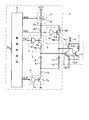
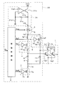
- FIG. 1 is an electrical configuration diagram showing the first embodiment.
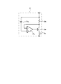
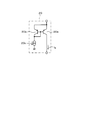
- FIG. 2 is an electrical configuration diagram of the constant current circuit.
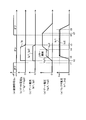
- FIG. 3 is a time chart of the gate current, the gate voltage, and the collector current with respect to the control signal.
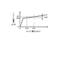
- FIG. 4 is an operation explanatory diagram for explaining the operation principle
- FIG. 5 is an action explanatory diagram showing mathematical formulas for explaining the operation principle
- FIG. 6 is an electrical configuration diagram of the constant current circuit showing the second embodiment.
- FIG. 7 is an electrical configuration diagram showing the third embodiment.
- FIG. 8 is an electrical configuration diagram showing the fourth embodiment.
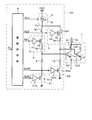
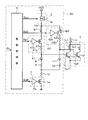
- FIG. 9 is an electrical configuration diagram showing the fifth embodiment.
- FIG. 10 is an electrical configuration diagram showing the sixth embodiment.
- FIG. 11 is an electrical configuration diagram showing the seventh embodiment.
- the semiconductor element portion 1 is provided in a state where IGBTs (Insulated Gate Bipolar Transistors) 1a and 1b having the same size are connected in parallel as a plurality of gate drive type semiconductor elements.
- the IGBTs 1a and 1b are configured to supply power from the power source to the load with the collector-emitter connected in common.
- the IGBTs 1a and 1b are given drive signals from the gate drive device 2 to their gates.
- the constant current circuit 3 is connected to the DC power supply VCC, the gate current Ig 1 is supplied to the gate of the IGBT 1 through the drive circuit 4, and the gate current Ig 2 is supplied to the gate of the IGBT 2 through the drive circuit 5. Supplied.
- the constant current circuit 3 is configured to supply a DC power supply VCC to a P-channel type MOSFET 3a via a resistor 3b.
- the MOSFET 3a is supplied with a gate drive signal from the differential amplifier 3c.
- the inverting input terminal of the differential amplifier 3c is connected to the source of the MOSFET 3a, and the non-inverting input terminal is connected to the DC power supply VCC via the reference power supply 7d.
- the differential amplifier 3c drives the MOSFET 3a so that the voltage between the terminals of the resistor 3b and the reference voltage Vref of the reference power supply 7d are equal.
- the constant current Ig set by the reference voltage Vref flows through the MOSFET 3a.
- This constant current Ig is supplied as the gate currents Ig1 and Ig2 of the IGBTs 1a and 1b.
- the constant current circuit 3 operates by receiving a drive signal Son from the drive control unit 6.
- the drive circuit 4 has a configuration in which a P-channel type MOSFET 4a and a resistor 4b are connected in series, and the MOSFET 4a is supplied with a gate drive signal from a driver 4c.
- the drive circuit 5 has a configuration in which a P-channel type MOSFET 5a and a resistor 5b are connected in series.
- the MOSFET 5a is supplied with a gate drive signal from a driver 5c.
- the drivers 4c and 5c are given drive signals Sg1 and Sg2 from the drive controller 6, respectively.
- the OFF circuit 7 is a circuit that turns off the IGBTs 1a and 1b at the same time, and includes an N-channel MOSFET 7a and a driver 7b that provides a gate signal.
- the gate of the IGBT 1a is connected to the MOSFET 7a of the off circuit 7 through a diode 8 and resistors 9, 10 in series.
- the gate of the IGBT 1b is connected to the MOSFET 7a of the off circuit 7 through the diode 11 and the resistors 12 and 10 in series.
- the MOSFET 7a discharges the gate charge of the IGBT 1a to the ground by the ON operation.
- the driver 7b is supplied with a drive signal Soff of the off operation from the drive control unit 6.
- the drive control unit 6 gives an ON signal Son to the constant current circuit 3 and gives drive signals Sg1 and Sg2 to the drive circuits 4 and 5.
- the constant current circuit 3 turns on the MOSFET 3a and supplies the constant current Ig set by the reference power supply 7d.
- the MOSFETs 4a and 5a are fully turned on by the drive signals Sg1 and Sg2. That is, the MOSFETs 4a and 5a are both operated in the saturation region when a sufficient gate voltage is applied.
- substantially the same gate currents Ig1 and Ig2 can be supplied to the gates of the IGBTs 1a and 1b even when the gate voltages are different due to characteristic variations.
- the two IGBTs 1a and 1b can be made to flow while sharing substantially the same collector currents Ic1 and Ic2.
- FIG. 3 shows the time transition of the gate current, gate voltage, and collector current of the IGBTs 1a and 1b operated by the control signal Sc in the above operation.
- the drive control unit 6 gives the drive signal Son to the constant current circuit 3 and drives it.
- the drive signals Sg1 and Sg2 are given to the drive circuits 4 and 5 at time t2.
- the constant current Ig supplied by the constant current circuit 3 is branched to the drive circuits 4 and 5 as shown in FIG. 3C, and the gates of the IGBTs 1a and 1b. Are supplied as gate currents Ig1 and Ig2.
- the MOSFETs 4a and 5a are driven in a full-on state according to the drive signals Sg1 and Sg2.
- IGBTs 1a and 1b are supplied with gate currents Ig1 and Ig2, respectively, and are driven at a constant current.
- collector currents Ic1 and Ic2 begin to flow.
- the gate currents Ig1 and Ig2 can be set to substantially the same current for the reason described later.
- the collector currents Ic1 and Ic2 of the IGBTs 1a and 1b can be driven in a state where the currents are substantially equal to each other.
- the gate voltages Vg1 and Vg2 of the IGBTs 1a and 1b start to rise again due to the feeding of the gate currents Ig1 and Ig2, and the gate currents Ig1 and Ig2 become zero when the predetermined gate voltage is reached at time t5. .
- the two IGBTs 1a and 1b are driven with substantially the same collector currents Ic1 and Ic2, and are driven with the entire current equally shared.
- drive control unit 6 stops drive signals Son, Sg1, and Sg2 to constant current circuit 3 and drive circuits 4 and 5. Then, the voltage application to the gates of the IGBTs 1a and 1b is stopped. Further, the drive control unit 6 outputs an off signal Soff to the off circuit 7 at time t7. Thereby, the MOSFET 7a of the off circuit 7 is turned on to form a path for discharging the charges of the gates of the two IGBTs 1a and 1b.
- IGBT 1a The gate charge of IGBT 1a is discharged through diode 8, resistors 9, 10 and MOSFET 7a, and the gate charge of IGBT 1b is discharged through diode 11, resistor 12, 10 and MOSFET 7a.
- gate voltages Vg1 and Vg2 become lower than threshold voltages Vt1 and Vt2 at time t8, collector currents Ic1 and Ic2 are also lowered, and IGBTs 1a and 1b shift to an off state.
- FIG. 4 shows the relationship between the drain-source voltage Vd and the drain current Id when the MOSFET is driven with a certain gate voltage.
- the drain current Id that flows when the gate voltage Vg is applied is expressed by the equation (1) in FIG. 5, W is the channel width, L is the channel length, Vt is the threshold voltage, ⁇ is the channel length modulation coefficient, ⁇ is the carrier mobility, and Co is the gate oxide film capacitance per unit area.
- Equation (1) shows the value of the drain current Id considering the channel length modulation coefficient ⁇ .
- the drain current Id when the drain voltage Vd is different, the drain current Id also changes, but this change amount ⁇ Id is relatively small.
- the difference ⁇ Id between the drain currents Id1 and Id2 can be expressed as shown in Expression (5). It can be expressed as in equation (6) using Vd1 and Vd2.
- the drain currents Id1 and Id2 of the MOSFETs 4a and 5a are the gate currents Ig1 and 1b of the IGBTs 1a and 1b in the present embodiment.
- the drain voltages Vd1 and Vd2 of the MOSFETs 4a and 5a are voltages obtained by subtracting the gate voltages Vg1 and Vd2 of the IGBTs 1a and 1b from the output voltage Va of the constant current circuit 3, respectively.
- the gate currents Ig1 and Ig2 can be expressed as follows:
- the gate currents Ig1 and Ig2 have different values from the above equation.
- the IGBTs 1a and 1b are driven by reducing the difference between the gate currents Ig1 and Ig2 due to the variations in the gate voltages Vg1 and Vg2 of the IGBTs 1a and 1b. Therefore, the collector currents Ic1 and Ic2 can be made to flow at an equal level.
- the two IGBTs 1a and 1b are connected in parallel to supply power to the load, the drive circuits 4 and 5 are provided, and the MOSFETs 4a and 5a are fully turned on to drive the gate currents of the IGBTs 1a and 1b. Since the configuration is such that Ig1 and Ig2 are supplied, even collector currents Ic1 and Ic2 can flow even when IGBTs 1a and 1b have characteristic variations.
- FIG. 6 shows the second embodiment, and the following description will be focused on differences from the first embodiment.
- a constant current circuit 20 is provided in place of the constant current circuit 3.
- a pnp transistor 20a for supplying a constant current Ig is provided, and a pnp transistor 20b is connected to the transistor 20a in a current mirror connection.
- the transistor 20b is provided so as to flow a predetermined current by the constant current circuit 20c, and has a configuration in which a current corresponding to the mirror ratio flows as the constant current Ig. Therefore, the same operational effects as those of the first embodiment can be obtained also by the second embodiment.
- FIG. 7 shows the third embodiment.
- the gate drive device 30 is configured to provide a constant voltage circuit 31 between the DC power supply VCC and the constant current circuit 4.
- the constant voltage circuit 31 suppresses fluctuations in the voltage of the DC power supply VCC and supplies the DC voltage VD with high accuracy to the constant current circuit 3.
- the collector-emitter of a pnp transistor 31a is connected between the DC power supply VCC and the constant current circuit 3.
- the base of the transistor 31a is given a base current by the differential amplifier 31b.
- a reference voltage Vref for outputting the output voltage VD is applied to the non-inverting input terminal of the differential amplifier 31b.
- a series circuit of resistors 31c and 31d is connected between the emitter of the transistor 31a and the ground. The common connection point of the resistors 31c and 31d is connected to the inverting input terminal of the differential amplifier 31b.
- the transistor 31a is supplied with the base current from the differential amplifier 31b so that the emitter voltage becomes VD. Therefore, the voltage VD can be supplied to the constant current circuit 3 with high accuracy.
- the constant voltage circuit 31 since the constant voltage circuit 31 is provided, in addition to the effects of the first embodiment, the voltage application to the gates of the IGBTs 1a and 1b can be performed with high accuracy by suppressing variation. Drive control can be performed.
- FIG. 8 shows the fourth embodiment.
- the gate drive device 40 is configured to provide drive circuits 41 and 42 instead of the drive circuits 4 and 5.
- the drive circuit 41 is configured such that the P-channel MOSFET 4a and the resistor 4b in the path from the constant current circuit 3 to the gate of the IGBT 1a are provided as they are.
- the MOSFET 4a is supplied with a gate signal from the differential amplifier 41a.
- the differential amplifier 41a is supplied with the reference voltage Vref1 at the inverting input terminal.
- a voltage dividing circuit of resistors 41b and 41c is connected between the drain of the MOSFET 4a and the ground, and a common connection point of the resistors 41b and 41c is connected to a non-inverting input terminal of the differential amplifier 41a.
- the drive circuit 42 has a configuration in which the P-channel MOSFET 5a and the resistor 5b in the path from the constant current circuit 3 to the gate of the IGBT 1b are provided as they are.
- the MOSFET 5a is supplied with a gate signal from the differential amplifier 51a.
- the differential amplifier 51a is supplied with the reference voltage Vref2 at its inverting input terminal.
- a voltage dividing circuit of resistors 42b and 42c is connected between the drain of the MOSFET 5a and the ground, and a common connection point of the resistors 42b and 42c is connected to a non-inverting input terminal of the differential amplifier 42a.
- the drive circuits 41 and 42 can perform feedback control with the differential amplifiers 41a and 42a while monitoring the drain voltage with respect to the MOSFETs 4a and 5a by the voltage dividing circuit.
- the MOSFETs 4a and 5a can be fully turned on accurately.
- the same effect as that of the first embodiment can be obtained.
- FIG. 9 shows the fifth embodiment.
- the gate drive device 50 is configured to provide off circuits 51 and 52 for individually turning off the IGBTs 1a and 1b in place of the off circuit 7.
- the off circuit 51 includes an N-channel MOSFET 51a and a driver 51b that provides a gate signal.
- the off circuit 52 includes an N-channel MOSFET 52a and a driver 52b that provides a gate signal. Further, the diodes 8 and 11 and the resistor 10 provided in the first embodiment are not provided.
- the IGBTs 1a and 1b can individually control the on / off operation. Also in this embodiment, the same effect as the first embodiment can be obtained.
- FIG. 10 shows the sixth embodiment.
- the gate drive device 60 is configured to provide drive circuits 61 and 62 instead of the drive circuits 4 and 5.
- the drive circuit 61 has a configuration in which an N-channel type MOSFET 61a and a resistor 61b are connected in series, and the MOSFET 61a receives a gate drive signal from a driver 61c.
- the drive circuit 62 has a configuration in which an N-channel type MOSFET 62a and a resistor 62b are connected in series, and the MOSFET 62a is supplied with a gate drive signal from a driver 62c.
- Drive signals Sg1 and Sg2 are given to the drivers 61c and 62c from the drive control unit 6, respectively.
- N-channel MOSFETs 61a and 62a are provided in the drive circuits 61 and 62, respectively, as switching elements for driving the gate.
- the MOSFETs 61a and 62a are driven on the high side so as to be fully turned on by the drivers 61c and 62c. Therefore, also according to the sixth embodiment, it is possible to obtain the same operational effects as those of the first embodiment.
- FIG. 11 shows the seventh embodiment.
- the gate drive device 70 is configured to provide drive circuits 71 and 72 instead of the drive circuits 4 and 5.
- the drive circuit 71 has a configuration in which a pnp bipolar transistor 71a and a resistor 71b are connected in series, and a base current is applied to the transistor 71a from a driver 71c.
- the drive circuit 72 has a configuration in which a pnp bipolar transistor 72a and a resistor 72b are connected in series, and the transistor 72a is supplied with a base current from a driver 72c.
- the drivers 71c and 72c are given drive signals Sg1 and Sg2 from the drive controller 6, respectively.
- the transistors 71a and 72a of the drive circuits 71 and 72 are controlled to operate in the saturation region when the base current is applied from the drivers 71c and 72c. As a result, the switching element is controlled to the full-on state. Therefore, also according to the seventh embodiment, it is possible to obtain the same operational effects as those of the first embodiment.
- the gate drive type semiconductor element is not limited to the IGBTs 1a and 1b, and may be configured to include three or more IGBTs. In addition to the IGBT, the gate drive type semiconductor element can also be applied to a MOSFET.
- an npn type bipolar transistor in addition to the P-channel type MOSFET, the N-channel type MOSFET, and the pnp type bipolar transistor, an npn type bipolar transistor can be used, and other switching elements can also be used.
Landscapes
- Engineering & Computer Science (AREA)
- Power Engineering (AREA)
- Power Conversion In General (AREA)
- Electronic Switches (AREA)
Abstract
Un dispositif de commande de grille qui commande une pluralité d'éléments semi-conducteurs de type à commande de grille (1a, 1b) connectés en parallèle comprend : un circuit à courant constant (3) pour fournir des courants constants aux grilles de la pluralité d'éléments semi-conducteurs ; une pluralité d'éléments de commutation (4a, 5a) disposés dans des trajets pour fournir des courants de grille aux grilles respectives de la pluralité d'éléments semi-conducteurs à partir du circuit à courant constant ; et une unité de commande d'excitation (6) pour commander l'excitation de la pluralité d'éléments de commutation de telle sorte que les courants constants fournis par le circuit à courant constant sont fournis aux grilles respectives de la pluralité d'éléments semi-conducteurs.
Priority Applications (2)
| Application Number | Priority Date | Filing Date | Title |
|---|---|---|---|
| CN201780072442.9A CN109983682A (zh) | 2016-11-25 | 2017-10-12 | 栅极驱动装置 |
| US16/389,026 US10601416B2 (en) | 2016-11-25 | 2019-04-19 | Gate drive device |
Applications Claiming Priority (2)
| Application Number | Priority Date | Filing Date | Title |
|---|---|---|---|
| JP2016-228961 | 2016-11-25 | ||
| JP2016228961A JP6601372B2 (ja) | 2016-11-25 | 2016-11-25 | ゲート駆動装置 |
Related Child Applications (1)
| Application Number | Title | Priority Date | Filing Date |
|---|---|---|---|
| US16/389,026 Continuation US10601416B2 (en) | 2016-11-25 | 2019-04-19 | Gate drive device |
Publications (1)
| Publication Number | Publication Date |
|---|---|
| WO2018096828A1 true WO2018096828A1 (fr) | 2018-05-31 |
Family
ID=62195463
Family Applications (1)
| Application Number | Title | Priority Date | Filing Date |
|---|---|---|---|
| PCT/JP2017/036988 Ceased WO2018096828A1 (fr) | 2016-11-25 | 2017-10-12 | Dispositif de commande de grille |
Country Status (4)
| Country | Link |
|---|---|
| US (1) | US10601416B2 (fr) |
| JP (1) | JP6601372B2 (fr) |
| CN (1) | CN109983682A (fr) |
| WO (1) | WO2018096828A1 (fr) |
Families Citing this family (2)
| Publication number | Priority date | Publication date | Assignee | Title |
|---|---|---|---|---|
| JP7052598B2 (ja) * | 2018-06-27 | 2022-04-12 | 株式会社デンソー | スイッチの駆動回路 |
| JP7119872B2 (ja) * | 2018-10-09 | 2022-08-17 | 株式会社デンソー | スイッチの駆動回路 |
Citations (3)
| Publication number | Priority date | Publication date | Assignee | Title |
|---|---|---|---|---|
| JP2002142445A (ja) * | 2000-11-07 | 2002-05-17 | Toshiba Corp | 電力変換装置 |
| JP2002369498A (ja) * | 2001-06-07 | 2002-12-20 | Fuji Electric Co Ltd | 電力用半導体素子のゲート駆動回路 |
| JP2014143788A (ja) * | 2013-01-22 | 2014-08-07 | Denso Corp | 電子装置 |
Family Cites Families (12)
| Publication number | Priority date | Publication date | Assignee | Title |
|---|---|---|---|---|
| JP4200535B2 (ja) * | 1998-02-27 | 2008-12-24 | ソニー株式会社 | 発光素子の駆動回路 |
| JP2002095240A (ja) * | 2000-09-18 | 2002-03-29 | Toshiba Corp | 絶縁ゲート型半導体素子のゲート駆動回路およびそれを用いた電力変換装置 |
| JP3857163B2 (ja) * | 2002-03-14 | 2006-12-13 | 株式会社東芝 | 広帯域増幅器、無線送受信装置及び半導体集積回路 |
| JP2004229382A (ja) * | 2003-01-21 | 2004-08-12 | Toshiba Corp | ゲート駆動回路、および電力変換装置 |
| US6879608B1 (en) * | 2003-03-31 | 2005-04-12 | Applied Micro Circuits Corporation | High compliance laser driver |
| JP5138287B2 (ja) * | 2007-06-27 | 2013-02-06 | 三菱電機株式会社 | ゲート駆動装置 |
| JP5854895B2 (ja) * | 2011-05-02 | 2016-02-09 | 三菱電機株式会社 | 電力用半導体装置 |
| JP5701176B2 (ja) * | 2011-08-04 | 2015-04-15 | 三菱電機株式会社 | ゲート駆動装置 |
| JP5337886B2 (ja) * | 2012-01-25 | 2013-11-06 | 株式会社フジクラ | Dc結合型レーザ駆動回路、及び、半導体レーザ素子の駆動方法 |
| CN104272594B (zh) * | 2012-05-01 | 2018-04-27 | 大岛俊蔵 | 过电流保护电源装置 |
| JP6089599B2 (ja) * | 2012-11-01 | 2017-03-08 | 富士電機株式会社 | 絶縁ゲート型半導体素子の駆動装置 |
| WO2015022860A1 (fr) * | 2013-08-12 | 2015-02-19 | 日産自動車株式会社 | Dispositif de commutation |
-
2016
- 2016-11-25 JP JP2016228961A patent/JP6601372B2/ja not_active Expired - Fee Related
-
2017
- 2017-10-12 WO PCT/JP2017/036988 patent/WO2018096828A1/fr not_active Ceased
- 2017-10-12 CN CN201780072442.9A patent/CN109983682A/zh active Pending
-
2019
- 2019-04-19 US US16/389,026 patent/US10601416B2/en active Active
Patent Citations (3)
| Publication number | Priority date | Publication date | Assignee | Title |
|---|---|---|---|---|
| JP2002142445A (ja) * | 2000-11-07 | 2002-05-17 | Toshiba Corp | 電力変換装置 |
| JP2002369498A (ja) * | 2001-06-07 | 2002-12-20 | Fuji Electric Co Ltd | 電力用半導体素子のゲート駆動回路 |
| JP2014143788A (ja) * | 2013-01-22 | 2014-08-07 | Denso Corp | 電子装置 |
Also Published As
| Publication number | Publication date |
|---|---|
| CN109983682A (zh) | 2019-07-05 |
| JP2018085885A (ja) | 2018-05-31 |
| US10601416B2 (en) | 2020-03-24 |
| JP6601372B2 (ja) | 2019-11-06 |
| US20190245536A1 (en) | 2019-08-08 |
Similar Documents
| Publication | Publication Date | Title |
|---|---|---|
| US10374594B2 (en) | Semiconductor device | |
| JP5862434B2 (ja) | パワートランジスタの駆動回路 | |
| JP5119894B2 (ja) | ドライバ回路 | |
| US9608622B2 (en) | Drive device for insulated-gate semiconductor element, and power converter | |
| US7839097B2 (en) | System and method for wide-range high-accuracy-low-dropout current regulation | |
| JP4935294B2 (ja) | 絶縁ゲート型デバイスの駆動回路 | |
| JP2014176228A (ja) | ゲート駆動回路 | |
| JP2014154669A (ja) | 過電流検出回路 | |
| CN109119418B (zh) | 半导体集成装置及其栅极筛查试验方法 | |
| JP6601372B2 (ja) | ゲート駆動装置 | |
| JP5348115B2 (ja) | 負荷駆動装置 | |
| KR101443178B1 (ko) | 전압제어회로 | |
| JP5666694B2 (ja) | 負荷電流検出回路 | |
| JP6572804B2 (ja) | ゲート駆動回路 | |
| US8692589B2 (en) | Semiconductor element driving circuit and semiconductor device | |
| KR20090087744A (ko) | 컨버터 | |
| JPH10145965A (ja) | 電流制限回路 | |
| JP2008282313A (ja) | 電源回路 | |
| JP2015022546A (ja) | 定電流定電圧回路 | |
| JPWO2016002329A1 (ja) | パワー半導体素子の電流検出装置 | |
| US11009899B2 (en) | Circuit and constant-current drive system having adjustable constant current output | |
| JP2010166359A (ja) | 電流制限回路 | |
| JP5000144B2 (ja) | 出力インピーダンス回路及びこれを適用した出力バッファ回路 | |
| JP2005346603A (ja) | 定電流回路 | |
| US20130093512A1 (en) | Power amplifier and operation controlling circuit thereof |
Legal Events
| Date | Code | Title | Description |
|---|---|---|---|
| 121 | Ep: the epo has been informed by wipo that ep was designated in this application |
Ref document number: 17873838 Country of ref document: EP Kind code of ref document: A1 |
|
| NENP | Non-entry into the national phase |
Ref country code: DE |
|
| 122 | Ep: pct application non-entry in european phase |
Ref document number: 17873838 Country of ref document: EP Kind code of ref document: A1 |