WO2018097410A1 - Boîtier de semiconducteur ayant une fiabilité élevée et son procédé de production - Google Patents
Boîtier de semiconducteur ayant une fiabilité élevée et son procédé de production Download PDFInfo
- Publication number
- WO2018097410A1 WO2018097410A1 PCT/KR2017/002403 KR2017002403W WO2018097410A1 WO 2018097410 A1 WO2018097410 A1 WO 2018097410A1 KR 2017002403 W KR2017002403 W KR 2017002403W WO 2018097410 A1 WO2018097410 A1 WO 2018097410A1
- Authority
- WO
- WIPO (PCT)
- Prior art keywords
- molding layer
- semiconductor chip
- frame
- hole
- layer
- Prior art date
- Legal status (The legal status is an assumption and is not a legal conclusion. Google has not performed a legal analysis and makes no representation as to the accuracy of the status listed.)
- Ceased
Links
Images


Classifications
-
- H—ELECTRICITY
- H10—SEMICONDUCTOR DEVICES; ELECTRIC SOLID-STATE DEVICES NOT OTHERWISE PROVIDED FOR
- H10W—GENERIC PACKAGES, INTERCONNECTIONS, CONNECTORS OR OTHER CONSTRUCTIONAL DETAILS OF DEVICES COVERED BY CLASS H10
- H10W20/00—Interconnections in chips, wafers or substrates
- H10W20/40—Interconnections external to wafers or substrates, e.g. back-end-of-line [BEOL] metallisations or vias connecting to gate electrodes
- H10W20/41—Interconnections external to wafers or substrates, e.g. back-end-of-line [BEOL] metallisations or vias connecting to gate electrodes characterised by their conductive parts
- H10W20/42—Vias, e.g. via plugs
-
- H—ELECTRICITY
- H10—SEMICONDUCTOR DEVICES; ELECTRIC SOLID-STATE DEVICES NOT OTHERWISE PROVIDED FOR
- H10W—GENERIC PACKAGES, INTERCONNECTIONS, CONNECTORS OR OTHER CONSTRUCTIONAL DETAILS OF DEVICES COVERED BY CLASS H10
- H10W74/00—Encapsulations, e.g. protective coatings
- H10W74/01—Manufacture or treatment
- H10W74/019—Manufacture or treatment using temporary auxiliary substrates
-
- H—ELECTRICITY
- H10—SEMICONDUCTOR DEVICES; ELECTRIC SOLID-STATE DEVICES NOT OTHERWISE PROVIDED FOR
- H10W—GENERIC PACKAGES, INTERCONNECTIONS, CONNECTORS OR OTHER CONSTRUCTIONAL DETAILS OF DEVICES COVERED BY CLASS H10
- H10W20/00—Interconnections in chips, wafers or substrates
- H10W20/40—Interconnections external to wafers or substrates, e.g. back-end-of-line [BEOL] metallisations or vias connecting to gate electrodes
- H10W20/41—Interconnections external to wafers or substrates, e.g. back-end-of-line [BEOL] metallisations or vias connecting to gate electrodes characterised by their conductive parts
- H10W20/435—Cross-sectional shapes or dispositions of interconnections
-
- H—ELECTRICITY
- H10—SEMICONDUCTOR DEVICES; ELECTRIC SOLID-STATE DEVICES NOT OTHERWISE PROVIDED FOR
- H10W—GENERIC PACKAGES, INTERCONNECTIONS, CONNECTORS OR OTHER CONSTRUCTIONAL DETAILS OF DEVICES COVERED BY CLASS H10
- H10W42/00—Arrangements for protection of devices
- H10W42/20—Arrangements for protection of devices protecting against electromagnetic or particle radiation, e.g. light, X-rays, gamma-rays or electrons
- H10W42/281—Arrangements for protection of devices protecting against electromagnetic or particle radiation, e.g. light, X-rays, gamma-rays or electrons characterised by their materials
- H10W42/284—Arrangements for protection of devices protecting against electromagnetic or particle radiation, e.g. light, X-rays, gamma-rays or electrons characterised by their materials shielding resins
-
- H—ELECTRICITY
- H10—SEMICONDUCTOR DEVICES; ELECTRIC SOLID-STATE DEVICES NOT OTHERWISE PROVIDED FOR
- H10W—GENERIC PACKAGES, INTERCONNECTIONS, CONNECTORS OR OTHER CONSTRUCTIONAL DETAILS OF DEVICES COVERED BY CLASS H10
- H10W42/00—Arrangements for protection of devices
- H10W42/60—Arrangements for protection of devices protecting against electrostatic charges or discharges, e.g. Faraday shields
-
- H—ELECTRICITY
- H10—SEMICONDUCTOR DEVICES; ELECTRIC SOLID-STATE DEVICES NOT OTHERWISE PROVIDED FOR
- H10W—GENERIC PACKAGES, INTERCONNECTIONS, CONNECTORS OR OTHER CONSTRUCTIONAL DETAILS OF DEVICES COVERED BY CLASS H10
- H10W70/00—Package substrates; Interposers; Redistribution layers [RDL]
- H10W70/01—Manufacture or treatment
- H10W70/05—Manufacture or treatment of insulating or insulated package substrates, or of interposers, or of redistribution layers
- H10W70/08—Manufacture or treatment of insulating or insulated package substrates, or of interposers, or of redistribution layers by depositing layers on the chip or wafer, e.g. "chip-first" RDLs
- H10W70/09—Manufacture or treatment of insulating or insulated package substrates, or of interposers, or of redistribution layers by depositing layers on the chip or wafer, e.g. "chip-first" RDLs extending onto an encapsulation that laterally surrounds the chip or wafer, e.g. fan-out wafer level package [FOWLP] RDLs
-
- H—ELECTRICITY
- H10—SEMICONDUCTOR DEVICES; ELECTRIC SOLID-STATE DEVICES NOT OTHERWISE PROVIDED FOR
- H10W—GENERIC PACKAGES, INTERCONNECTIONS, CONNECTORS OR OTHER CONSTRUCTIONAL DETAILS OF DEVICES COVERED BY CLASS H10
- H10W70/00—Package substrates; Interposers; Redistribution layers [RDL]
- H10W70/60—Insulating or insulated package substrates; Interposers; Redistribution layers
-
- H—ELECTRICITY
- H10—SEMICONDUCTOR DEVICES; ELECTRIC SOLID-STATE DEVICES NOT OTHERWISE PROVIDED FOR
- H10W—GENERIC PACKAGES, INTERCONNECTIONS, CONNECTORS OR OTHER CONSTRUCTIONAL DETAILS OF DEVICES COVERED BY CLASS H10
- H10W72/00—Interconnections or connectors in packages
- H10W72/20—Bump connectors, e.g. solder bumps or copper pillars; Dummy bumps; Thermal bumps
-
- H—ELECTRICITY
- H10—SEMICONDUCTOR DEVICES; ELECTRIC SOLID-STATE DEVICES NOT OTHERWISE PROVIDED FOR
- H10W—GENERIC PACKAGES, INTERCONNECTIONS, CONNECTORS OR OTHER CONSTRUCTIONAL DETAILS OF DEVICES COVERED BY CLASS H10
- H10W72/00—Interconnections or connectors in packages
- H10W72/30—Die-attach connectors
-
- H—ELECTRICITY
- H10—SEMICONDUCTOR DEVICES; ELECTRIC SOLID-STATE DEVICES NOT OTHERWISE PROVIDED FOR
- H10W—GENERIC PACKAGES, INTERCONNECTIONS, CONNECTORS OR OTHER CONSTRUCTIONAL DETAILS OF DEVICES COVERED BY CLASS H10
- H10W72/00—Interconnections or connectors in packages
- H10W72/90—Bond pads, in general
-
- H—ELECTRICITY
- H10—SEMICONDUCTOR DEVICES; ELECTRIC SOLID-STATE DEVICES NOT OTHERWISE PROVIDED FOR
- H10W—GENERIC PACKAGES, INTERCONNECTIONS, CONNECTORS OR OTHER CONSTRUCTIONAL DETAILS OF DEVICES COVERED BY CLASS H10
- H10W74/00—Encapsulations, e.g. protective coatings
- H10W74/01—Manufacture or treatment
- H10W74/016—Manufacture or treatment using moulds
-
- H—ELECTRICITY
- H10—SEMICONDUCTOR DEVICES; ELECTRIC SOLID-STATE DEVICES NOT OTHERWISE PROVIDED FOR
- H10W—GENERIC PACKAGES, INTERCONNECTIONS, CONNECTORS OR OTHER CONSTRUCTIONAL DETAILS OF DEVICES COVERED BY CLASS H10
- H10W74/00—Encapsulations, e.g. protective coatings
- H10W74/10—Encapsulations, e.g. protective coatings characterised by their shape or disposition
- H10W74/111—Encapsulations, e.g. protective coatings characterised by their shape or disposition the semiconductor body being completely enclosed
- H10W74/114—Encapsulations, e.g. protective coatings characterised by their shape or disposition the semiconductor body being completely enclosed by a substrate and the encapsulations
- H10W74/117—Encapsulations, e.g. protective coatings characterised by their shape or disposition the semiconductor body being completely enclosed by a substrate and the encapsulations the substrate having spherical bumps for external connection
-
- H—ELECTRICITY
- H10—SEMICONDUCTOR DEVICES; ELECTRIC SOLID-STATE DEVICES NOT OTHERWISE PROVIDED FOR
- H10W—GENERIC PACKAGES, INTERCONNECTIONS, CONNECTORS OR OTHER CONSTRUCTIONAL DETAILS OF DEVICES COVERED BY CLASS H10
- H10W74/00—Encapsulations, e.g. protective coatings
- H10W74/10—Encapsulations, e.g. protective coatings characterised by their shape or disposition
- H10W74/111—Encapsulations, e.g. protective coatings characterised by their shape or disposition the semiconductor body being completely enclosed
- H10W74/121—Encapsulations, e.g. protective coatings characterised by their shape or disposition the semiconductor body being completely enclosed by multiple encapsulations, e.g. by a thin protective coating and a thick encapsulation
-
- H—ELECTRICITY
- H10—SEMICONDUCTOR DEVICES; ELECTRIC SOLID-STATE DEVICES NOT OTHERWISE PROVIDED FOR
- H10W—GENERIC PACKAGES, INTERCONNECTIONS, CONNECTORS OR OTHER CONSTRUCTIONAL DETAILS OF DEVICES COVERED BY CLASS H10
- H10W74/00—Encapsulations, e.g. protective coatings
- H10W74/40—Encapsulations, e.g. protective coatings characterised by their materials
-
- H—ELECTRICITY
- H10—SEMICONDUCTOR DEVICES; ELECTRIC SOLID-STATE DEVICES NOT OTHERWISE PROVIDED FOR
- H10W—GENERIC PACKAGES, INTERCONNECTIONS, CONNECTORS OR OTHER CONSTRUCTIONAL DETAILS OF DEVICES COVERED BY CLASS H10
- H10W76/00—Containers; Fillings or auxiliary members therefor; Seals
- H10W76/10—Containers or parts thereof
- H10W76/17—Containers or parts thereof characterised by their materials
-
- H—ELECTRICITY
- H10—SEMICONDUCTOR DEVICES; ELECTRIC SOLID-STATE DEVICES NOT OTHERWISE PROVIDED FOR
- H10W—GENERIC PACKAGES, INTERCONNECTIONS, CONNECTORS OR OTHER CONSTRUCTIONAL DETAILS OF DEVICES COVERED BY CLASS H10
- H10W76/00—Containers; Fillings or auxiliary members therefor; Seals
- H10W76/40—Fillings or auxiliary members in containers, e.g. centering rings
-
- H—ELECTRICITY
- H10—SEMICONDUCTOR DEVICES; ELECTRIC SOLID-STATE DEVICES NOT OTHERWISE PROVIDED FOR
- H10W—GENERIC PACKAGES, INTERCONNECTIONS, CONNECTORS OR OTHER CONSTRUCTIONAL DETAILS OF DEVICES COVERED BY CLASS H10
- H10W90/00—Package configurations
-
- H—ELECTRICITY
- H10—SEMICONDUCTOR DEVICES; ELECTRIC SOLID-STATE DEVICES NOT OTHERWISE PROVIDED FOR
- H10W—GENERIC PACKAGES, INTERCONNECTIONS, CONNECTORS OR OTHER CONSTRUCTIONAL DETAILS OF DEVICES COVERED BY CLASS H10
- H10W70/00—Package substrates; Interposers; Redistribution layers [RDL]
- H10W70/01—Manufacture or treatment
- H10W70/05—Manufacture or treatment of insulating or insulated package substrates, or of interposers, or of redistribution layers
-
- H—ELECTRICITY
- H10—SEMICONDUCTOR DEVICES; ELECTRIC SOLID-STATE DEVICES NOT OTHERWISE PROVIDED FOR
- H10W—GENERIC PACKAGES, INTERCONNECTIONS, CONNECTORS OR OTHER CONSTRUCTIONAL DETAILS OF DEVICES COVERED BY CLASS H10
- H10W70/00—Package substrates; Interposers; Redistribution layers [RDL]
- H10W70/60—Insulating or insulated package substrates; Interposers; Redistribution layers
- H10W70/62—Insulating or insulated package substrates; Interposers; Redistribution layers characterised by their interconnections
- H10W70/65—Shapes or dispositions of interconnections
- H10W70/652—Cross-sectional shapes
-
- H—ELECTRICITY
- H10—SEMICONDUCTOR DEVICES; ELECTRIC SOLID-STATE DEVICES NOT OTHERWISE PROVIDED FOR
- H10W—GENERIC PACKAGES, INTERCONNECTIONS, CONNECTORS OR OTHER CONSTRUCTIONAL DETAILS OF DEVICES COVERED BY CLASS H10
- H10W70/00—Package substrates; Interposers; Redistribution layers [RDL]
- H10W70/60—Insulating or insulated package substrates; Interposers; Redistribution layers
- H10W70/62—Insulating or insulated package substrates; Interposers; Redistribution layers characterised by their interconnections
- H10W70/65—Shapes or dispositions of interconnections
- H10W70/654—Top-view layouts
- H10W70/655—Fan-out layouts
-
- H—ELECTRICITY
- H10—SEMICONDUCTOR DEVICES; ELECTRIC SOLID-STATE DEVICES NOT OTHERWISE PROVIDED FOR
- H10W—GENERIC PACKAGES, INTERCONNECTIONS, CONNECTORS OR OTHER CONSTRUCTIONAL DETAILS OF DEVICES COVERED BY CLASS H10
- H10W70/00—Package substrates; Interposers; Redistribution layers [RDL]
- H10W70/60—Insulating or insulated package substrates; Interposers; Redistribution layers
- H10W70/67—Insulating or insulated package substrates; Interposers; Redistribution layers characterised by their insulating layers or insulating parts
- H10W70/68—Shapes or dispositions thereof
- H10W70/682—Shapes or dispositions thereof comprising holes having chips therein
-
- H—ELECTRICITY
- H10—SEMICONDUCTOR DEVICES; ELECTRIC SOLID-STATE DEVICES NOT OTHERWISE PROVIDED FOR
- H10W—GENERIC PACKAGES, INTERCONNECTIONS, CONNECTORS OR OTHER CONSTRUCTIONAL DETAILS OF DEVICES COVERED BY CLASS H10
- H10W72/00—Interconnections or connectors in packages
- H10W72/01—Manufacture or treatment
- H10W72/0198—Manufacture or treatment batch processes
-
- H—ELECTRICITY
- H10—SEMICONDUCTOR DEVICES; ELECTRIC SOLID-STATE DEVICES NOT OTHERWISE PROVIDED FOR
- H10W—GENERIC PACKAGES, INTERCONNECTIONS, CONNECTORS OR OTHER CONSTRUCTIONAL DETAILS OF DEVICES COVERED BY CLASS H10
- H10W72/00—Interconnections or connectors in packages
- H10W72/20—Bump connectors, e.g. solder bumps or copper pillars; Dummy bumps; Thermal bumps
- H10W72/241—Dispositions, e.g. layouts
-
- H—ELECTRICITY
- H10—SEMICONDUCTOR DEVICES; ELECTRIC SOLID-STATE DEVICES NOT OTHERWISE PROVIDED FOR
- H10W—GENERIC PACKAGES, INTERCONNECTIONS, CONNECTORS OR OTHER CONSTRUCTIONAL DETAILS OF DEVICES COVERED BY CLASS H10
- H10W72/00—Interconnections or connectors in packages
- H10W72/851—Dispositions of multiple connectors or interconnections
- H10W72/853—On the same surface
- H10W72/856—Bump connectors and die-attach connectors
-
- H—ELECTRICITY
- H10—SEMICONDUCTOR DEVICES; ELECTRIC SOLID-STATE DEVICES NOT OTHERWISE PROVIDED FOR
- H10W—GENERIC PACKAGES, INTERCONNECTIONS, CONNECTORS OR OTHER CONSTRUCTIONAL DETAILS OF DEVICES COVERED BY CLASS H10
- H10W72/00—Interconnections or connectors in packages
- H10W72/851—Dispositions of multiple connectors or interconnections
- H10W72/874—On different surfaces
-
- H—ELECTRICITY
- H10—SEMICONDUCTOR DEVICES; ELECTRIC SOLID-STATE DEVICES NOT OTHERWISE PROVIDED FOR
- H10W—GENERIC PACKAGES, INTERCONNECTIONS, CONNECTORS OR OTHER CONSTRUCTIONAL DETAILS OF DEVICES COVERED BY CLASS H10
- H10W72/00—Interconnections or connectors in packages
- H10W72/90—Bond pads, in general
- H10W72/941—Dispositions of bond pads
- H10W72/9413—Dispositions of bond pads on encapsulations
-
- H—ELECTRICITY
- H10—SEMICONDUCTOR DEVICES; ELECTRIC SOLID-STATE DEVICES NOT OTHERWISE PROVIDED FOR
- H10W—GENERIC PACKAGES, INTERCONNECTIONS, CONNECTORS OR OTHER CONSTRUCTIONAL DETAILS OF DEVICES COVERED BY CLASS H10
- H10W74/00—Encapsulations, e.g. protective coatings
- H10W74/01—Manufacture or treatment
- H10W74/014—Manufacture or treatment using batch processing
-
- H—ELECTRICITY
- H10—SEMICONDUCTOR DEVICES; ELECTRIC SOLID-STATE DEVICES NOT OTHERWISE PROVIDED FOR
- H10W—GENERIC PACKAGES, INTERCONNECTIONS, CONNECTORS OR OTHER CONSTRUCTIONAL DETAILS OF DEVICES COVERED BY CLASS H10
- H10W90/00—Package configurations
- H10W90/701—Package configurations characterised by the relative positions of pads or connectors relative to package parts
- H10W90/721—Package configurations characterised by the relative positions of pads or connectors relative to package parts of bump connectors
- H10W90/722—Package configurations characterised by the relative positions of pads or connectors relative to package parts of bump connectors between stacked chips
-
- H—ELECTRICITY
- H10—SEMICONDUCTOR DEVICES; ELECTRIC SOLID-STATE DEVICES NOT OTHERWISE PROVIDED FOR
- H10W—GENERIC PACKAGES, INTERCONNECTIONS, CONNECTORS OR OTHER CONSTRUCTIONAL DETAILS OF DEVICES COVERED BY CLASS H10
- H10W90/00—Package configurations
- H10W90/701—Package configurations characterised by the relative positions of pads or connectors relative to package parts
- H10W90/721—Package configurations characterised by the relative positions of pads or connectors relative to package parts of bump connectors
- H10W90/724—Package configurations characterised by the relative positions of pads or connectors relative to package parts of bump connectors between a chip and a stacked insulating package substrate, interposer or RDL
-
- H—ELECTRICITY
- H10—SEMICONDUCTOR DEVICES; ELECTRIC SOLID-STATE DEVICES NOT OTHERWISE PROVIDED FOR
- H10W—GENERIC PACKAGES, INTERCONNECTIONS, CONNECTORS OR OTHER CONSTRUCTIONAL DETAILS OF DEVICES COVERED BY CLASS H10
- H10W90/00—Package configurations
- H10W90/701—Package configurations characterised by the relative positions of pads or connectors relative to package parts
- H10W90/731—Package configurations characterised by the relative positions of pads or connectors relative to package parts of die-attach connectors
- H10W90/734—Package configurations characterised by the relative positions of pads or connectors relative to package parts of die-attach connectors between a chip and a stacked insulating package substrate, interposer or RDL
Definitions
- the present invention relates to a semiconductor package and a method for manufacturing the same, and more particularly, to a semiconductor package and a method for manufacturing the same that can ensure high reliability using an insulating frame.
- the size of semiconductor chips is being reduced. Reduction of the size of the semiconductor chip means that the area of one semiconductor chip which performs an independent function is reduced.
- the semiconductor chip is required to have high reliability in the use environment. The semiconductor chip with high reliability maintains its electrical characteristics even when used for a long time, and stably operates within a specific range even with a change in external temperature. In addition, changes in electrical properties should be minimized for various chemical or mechanical factors introduced from the external environment.
- a package is a manufacturing technology that can package semiconductor chips to protect the semiconductor chips from the external environment and to ensure stable operation.
- the conditions required for the semiconductor package in the use environment are various, have a small area and thickness, it is required to minimize the variation of the characteristics due to the influence of the external environment.
- the semiconductor chip since various circuits are implemented in one semiconductor chip, the semiconductor chip has a plurality of pads.
- the plurality of pads are electrically connected to external connection terminals in the semiconductor package.
- the external connection terminal is electrically connected to the printed circuit board provided in the use environment.
- a fan-out package is developed in which external connection terminals are arranged to extend beyond an area occupied by a semiconductor chip.
- the fan-out package is a package type in which a molding material is extended to a semiconductor chip side region and a redistribution layer is formed on the molding material.
- the package type is provided in a form in which a molding material surrounds an outer portion of the semiconductor chip.
- the package is composed of only the molding material due to the tendency of the thickness of the semiconductor chip is reduced, there is a certain limit to protect the semiconductor chip from mechanical stress, etc., there is a problem that does not sufficiently protect the semiconductor chip from external moisture, etc. do.
- the molding material has an insulating polymer as a main component, there is a problem that the polymer chain is loosened due to an aging phenomenon in a continuous use environment, and the mechanical strength and chemical resistance of the material decrease.
- a metal frame is used.
- the metal frame is provided to surround the molding material and the outside of the semiconductor chip in the manufacturing process.
- the metal frame has low chemical resistance due to oxidation in the atmosphere.
- the ductility and malleability of the semiconductor package in the manufacturing process causes the phenomenon.
- the first technical problem to be achieved by the present invention is to provide a semiconductor package with improved reliability.
- Another object of the present invention is to provide a method of manufacturing a semiconductor package for achieving the first technical problem.
- the insulating frame having a first surface and a second surface facing the first surface; A semiconductor chip disposed in the through hole of the insulating frame; A molding layer filling the semiconductor chip disposed in the through hole; And a redistribution layer electrically connected to the pad on the active surface of the semiconductor chip, the redistribution layer formed to extend on the first surface of the insulating frame, A semiconductor package is provided, characterized in that the width of the molding layer in the lateral extension region on the back side of the semiconductor chip is greater than the width of the molding layer.
- the first through-hole and the second surface formed from the first surface by etching a frame led having a first surface and a second surface facing the first surface Forming a second through hole formed from and having a width greater than that of the first through hole; Disposing a semiconductor chip in the through hole according to the etching of the frame ledger; Forming a molding layer filling the through hole in which the semiconductor chip is disposed; And forming a redistribution layer electrically connected to a pad on an active surface of the semiconductor chip which is coplanar with the first surface of the frame ledger.
- the semiconductor chip and the molding layer is accommodated, the frame on which the redistribution layer is formed of an insulating material.
- the use of an insulating frame can ensure strong chemical resistance compared to the use of a conventional metal frame.
- a short circuit phenomenon with an adjacent package or a short circuit phenomenon with a lower wiring pattern is prevented.
- the insulating frame has a first through hole and a second through hole therein.
- the semiconductor chip is mounted through the first through hole. Deformation of the semiconductor package due to stress due to various causes is minimized through the insulating frame disposed on the side of the semiconductor chip. In addition, heat generated in the semiconductor chip by the molding layer filling the second through hole may be easily discharged to the outside.
- the surface of the insulating frame may be modified with a reinforcing material in order to effectively distribute stress and secure mechanical strength.
- a buffer layer is formed between the insulating frame and the molding layer to perform stress absorption.
- the molding layers may have different conductivity, and conductive particles are added to the second molding layer formed on the back surface of the semiconductor chip. As a result, electromagnetic shielding is achieved and malfunction of the semiconductor chip due to electromagnetic interference is prevented.
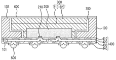
- FIG. 1 is a cross-sectional view illustrating a semiconductor package according to a first embodiment of the present invention.
- FIG. 2 to 7 are cross-sectional views and plan views illustrating a method of manufacturing the semiconductor package of FIG. 1 according to the first embodiment of the present invention.
- FIG. 8 and 9 are cross-sectional views illustrating various cutting examples of the frame ledger of FIG. 6 according to the first embodiment of the present invention.
- 10 to 13 are cross-sectional views illustrating a semiconductor package and a method of manufacturing the same according to the second embodiment of the present invention.
- 14 to 16 are cross-sectional views illustrating a semiconductor package and a method of manufacturing the same according to a third embodiment of the present invention.
- 17 to 19 are cross-sectional views illustrating a semiconductor package and a method of manufacturing the same according to a fourth embodiment of the present invention.
- 20 is a cross-sectional view for describing a semiconductor package and a method of manufacturing the same according to the fifth embodiment of the present invention.
- FIG. 1 is a cross-sectional view illustrating a semiconductor package according to a first embodiment of the present invention.
- the semiconductor package according to the present exemplary embodiment includes an insulating frame 100, a semiconductor chip 200, a molding layer 300, a redistribution layer 400, an external connection terminal 500, and a protective film 600. .
- the insulating frame 100 is an insulating material, and preferably has a coefficient of thermal expansion similar to that of the carrier substrate or the molding layer described above. Therefore, the insulating frame 100 may be an insulating ceramic or a ceramic of semiconductor material.
- the insulating ceramic may have various materials, such as metal oxide or metal nitride, and soda lime glass or sapphire may be used.
- the ceramic material of the semiconductor material may have a silicon material, and in addition, ZnO, GaN, and GaAs may be used. Since the ceramic material of the semiconductor material is insulated in an undoped state, the undoped material may be used.
- the insulating frame 100 may be variously selected according to the material of the carrier substrate or the molding layer 300 used.
- soda-lime glass has a coefficient of thermal expansion of 9 ⁇ 9.5 ppm / °C, which can be minimized thermal stress between the insulating frame 100 and the molding layer 300 with a coefficient of thermal expansion in the range similar to EMC.
- the insulating frame 100 is required to be wider than the width of the upper first surface 101 of the lower second surface (102).
- the width of the inner circumferential surface of the insulating frame 100 formed from the first surface 101 toward the second surface 102 is set differently depending on the position.
- the insulating frame 100 may be made of the same material, but may be divided into a first insulating frame 110 and a second insulating frame 120 by a shape.
- the first insulating frame 110 includes a first surface 101 and forms a first through hole by the inner circumferential surface.
- the second insulating frame 120 is defined on the first insulating frame 110 and forms a second through hole by the inner circumferential surface.
- the first through hole has a smaller width than the second through hole.
- the semiconductor chip 200 is disposed in the first through hole.
- the active surface on which the pad 210 of the semiconductor chip 200 is formed is preferably coplanar with the first surface 101.
- the thickness of the semiconductor chip 200 may be equal to or different from the thickness of the first insulating frame 110. That is, in FIG. 1, the thickness of the semiconductor chip 200 is greater than the thickness of the first insulating frame 110, but the thickness of the semiconductor chip 200 is equal to the thickness of the first insulating frame 110. It may be small or small.
- the molding layer 300 is buried between the semiconductor chip 200 and the insulating frame 100.
- the molding layer 300 fills the first through hole and the second through hole.
- the molding layer 300 filling the through holes may be formed on the same plane as the second surface 102 of the insulating frame 100.
- the molding layer 300 is composed of an EMC (Epoxy Molding Compound), it is provided with a mixture of an insulating polymer and an inorganic material silica powder and the like.
- a conductive powder may be added to the molding layer 300.
- the space between the second surface 102 of the insulating frame 100 is filled more than the width of the molding layer 300 filling the first surface 101 of the insulating frame 100 and the semiconductor chip 200.
- the width of the molding layer 300 is set larger. That is, the molding layer filling the gap between the points where the second surface 102 is formed from the area on the back surface of the semiconductor chip 300 than the width of the molding layer 300 filling the side surface of the semiconductor chip 200 ( The width of 300) is set larger.
- the redistribution layer 400 is formed on the active surface of the semiconductor chip 200 or the first surface 101 of the insulating frame 100.
- the redistribution layer 400 formed includes a first insulating layer 410, a first wiring layer 420, a second insulating layer 430, and a second wiring layer 440.
- the configuration of the redistribution layer 400 is merely an example configured to realize the fan-out structure, and the configuration of the redistribution layer 400 described above may be variously changed according to those skilled in the art.
- the redistribution layer 400 is capable of forming the external connection terminal 500 in an area outside the area occupied by the semiconductor chip 200
- any type of redistribution layer 400 may be employed.
- the first wiring layer 420 extends beyond the area occupied by the semiconductor chip 200 and extends to the lower region of the insulating frame 100.
- the first wiring layer 420 is formed in the molding layer 300 region. In the case of extending to will be possible in this embodiment.
- the redistribution layer 400 is electrically connected to the external connection terminal 500.
- the external connection terminal 500 has a structure of solder balls or bumps.
- the external connection terminal 500 is formed on the second wiring layer 440 and is electrically connected to the pad 210 of the semiconductor chip 200.
- the second wiring layer 440 may be omitted. That is, the external connection terminal 500 may be directly formed on the first wiring layer 420.
- the protective film 600 may be provided on the second surface 102 of the insulating frame 100 and the molding layer 300 forming the same plane.
- the protective film 600 is to protect the molding layer 300 from the external environment and may be provided to prevent mechanical damage and infiltration of moisture.
- the protective film 600 may be an insulating film and may have a material of epoxy or acrylic.
- the semiconductor chip 200 is mounted into a first through hole defined by the first insulating frame 110.
- the upper second insulating frame 120 defines a second through hole having a wider width than the first through hole.
- the first insulating frame 110 disposed on the side surface of the semiconductor chip 200 has a larger width than the second insulating frame 120.
- Heat generated during use of the semiconductor chip 200 induces thermal expansion in the molding layer 300.
- thermal deformation of the molding layer 300 formed on the side surface of the semiconductor chip 200 causes structural deformation of the semiconductor package. Therefore, the first insulating frame 110 disposed on the side surface and having a relatively large thickness blocks the stress due to thermal expansion of the semiconductor package.
- the insulating frame 100 of an insulating material has a property that is insufficient to perform the heat transfer to the outside smoothly. This can be solved through the second through hole having a relatively wide width. That is, the molding layer 300 filling the second through hole may smoothly discharge heat generated from the semiconductor chip 200 to the outside of the semiconductor package.
- FIG. 2 to 7 are cross-sectional views and plan views illustrating a method of manufacturing the semiconductor package of FIG. 1 according to the first embodiment of the present invention.
- the frame ledger 10 is prepared.
- the second surface 102 of the frame ledger 10 is etched to form a second through hole 121 defined by the second insulating frame 120.
- the portion exposed by the second through hole 121 is further etched to form a first through hole 111 having a narrower width than the second through hole 121.
- the formation of the first through hole 111 and the formation of the second through hole 121 may be performed regardless of the order. That is, the first surface 101 of the frame ledger 10 is etched to form the first through hole 111, and then the second surface 102 facing the first surface 101 is etched to form the first through hole.
- the second through hole 121 having a wider width than the ball 111 may be formed.
- two frame ledgers may be joined to form the frame ledger shown in FIG. 3.
- the frame ledger having the first through hole and the frame ledger having the second through hole may be joined to form the frame ledger shown in FIG. 3.
- FIG. 4 is a bottom plan view illustrating the frame ledger shown in FIG. 3.
- the inner region of the frame ledger 10 defined by the solid line is defined as the first through hole 111, and the inner region of the frame ledger 100 defined by the dotted line is the second through hole ( 121).
- the semiconductor chip is mounted in the first through hole 111 and the molding layer is embedded.
- the frame ledger 10 illustrated in FIG. 3 is disposed on the carrier substrate 20.
- the semiconductor chip 200 is disposed in the through hole of the frame ledger 10.
- an adhesive layer or an adhesive layer may be interposed between the semiconductor chip 200 and the carrier substrate 20.
- the adhesive layer or the adhesive layer may be provided in the form of a film that is easily removable.
- an active surface on which the pads 210 and the like are disposed faces the carrier substrate 20, and a rear surface of the semiconductor chip 200 facing the active substrate is opened upward.
- the height at which the back surface of the semiconductor chip 200 is located may be greater than the height of the first through hole in the frame ledger 10.
- the height at which the rear surface of the semiconductor chip 200 is located may be the same as or lower than the height of the first through hole in the frame ledger 20. This means that the semiconductor chip 200 disposed in the through hole of the frame ledger 10 may be completely included in the first through hole, and may be disposed up to a part of the second through hole beyond the first through hole.
- the epoxy molding compound (EMC) constituting the molding layer 300 may have a conventional material. That is, it may have a material containing an insulating polymer, silica powder or carbon black.
- the protective film 600 may be attached to the second surface 102 of the frame ledger 10 and the upper portion of the molding layer 300.
- the protective film 600 absorbs moisture resistance and external mechanical shock.
- the semiconductor chip 200 having the active surface facing the carrier substrate 20 is disposed in the first through hole, and according to the embodiment, a part of the second through hole is formed on the carrier substrate 20. Are placed over.
- the semiconductor chip 200 is shielded by the molding layer 300 by the molding layer 300 filling the through hole.
- a redistribution layer 400 is formed on the pad 210 of the semiconductor chip 200 and the first surface 101 of the frame ledger 10.
- the frame ledger 10 in which the molding layer 300 is formed is separated from the carrier substrate.
- the pad 210 of the semiconductor chip 200 and the first surface 101 of the frame ledger 10 are exposed by separation from the carrier substrate.
- the redistribution layer 400 and the external connection terminal 500 are sequentially formed on the pad 210 of the semiconductor chip 200 and the first surface 101 of the frame ledger 10.
- Formation of the redistribution layer 400 is in accordance with a conventional manufacturing process. That is, the first insulating layer 410 is formed by deposition, and the pad 210 of the semiconductor chip 200 is exposed by selective etching of the first insulating layer 410. Subsequently, a first wiring layer 420 is formed on the first insulating film 410. The first wiring layer 420 is electrically connected to the pad 210 of the semiconductor chip 200, and a part of the first wiring layer 420 is in physical contact with the pad 210. In addition, the first wiring layer 420 is formed to extend to a region other than the semiconductor chip 200 region.
- a second insulating layer 430 is formed on the first wiring layer 420, and a second wiring layer 440 is formed to be electrically connected to the first wiring layer 420 by selective etching and a conventional deposition process. That is, a part of the first wiring layer 420 is exposed in a specific region by performing selective etching on the second insulating layer 430. Subsequently, when a metal deposition process is performed, the first wiring layer 420 is electrically connected to the second wiring layer 440.
- an external connection terminal 500 is formed on the second wiring layer 440 of the redistribution layer 400.
- the external connection terminal 500 is preferably a solder ball or bump.
- the semiconductor chip 200 is mounted in the first through hole 111 of the frame ledger 10, and a molding layer 300 filling the through holes is formed.
- the redistribution layer 400 is formed on the active surface of the semiconductor chip 200 and the first surface 101 of the frame ledger 10.
- an individualized semiconductor package may be obtained by cutting the frame ledger 10 along the cutting line A-A '.
- the semiconductor package illustrated in FIG. 1 may be obtained by cutting the frame ledger 10 having the through-holes accommodating the semiconductor chip 200 and the molding layer 300 shielding the semiconductor chip 200. .
- FIG. 8 and 9 are cross-sectional views illustrating various cutting examples of the frame ledger of FIG. 6 according to the first embodiment of the present invention.
- the semiconductor package manufactured by cutting the frame ledger 10 has a shape other than the semiconductor package shown in FIG. 1.
- the cutting is performed along the cutting line B-B ′, and the cutting is performed to a part of the molding layer 300 filling the second through hole, and a part of the first insulating frame 110 is cut by the cutting line. Remaining in the semiconductor package. Therefore, portions of the first insulating frame 110 remain on both side surfaces of the lower portion of the semiconductor package.
- the lower region of the molding layer 300 is shielded by side portions of the first insulating frame 110, and the upper region of the molding layer 300 is exposed to the outside.
- the first insulating frame 110 surrounding the lower region of the molding layer 300 illustrated in FIG. 8 blocks thermal deformation caused by the use of the semiconductor chip 200.
- the side surface of the semiconductor chip 300 is protected from the external environment.
- the cutting of the frame ledger 10 disposed between the adjacent semiconductor chips 200 is buried between the first insulating frame 110 and the semiconductor chip 200 along the cutting line C-C ′. Is performed for the molding layer 300.
- the side surface of the molding layer 300 formed on the side surface of the semiconductor chip 200 is exposed.
- the upper surface of the molding layer 300 filling the upper portion of the semiconductor chip 200 by cutting is also exposed.
- an insulating frame is used in the manufacturing process. In the manufacturing process using the insulating frame, deformation of the frame ledger due to thermal stress generated during molding is minimized.
- the semiconductor package manufactured through the process of FIGS. 8 and 9 may be a fan-in type in which external connection terminals are limited to semiconductor chip regions.
- 10 to 13 are cross-sectional views illustrating a semiconductor package and a method of manufacturing the same according to the second embodiment of the present invention.
- the semiconductor package of the present embodiment is the same as that of FIG. 1 except for the configuration of the molding layer 300.
- the molding layer 300 has a first molding layer 310 and a second molding layer 320.
- the first molding layer 310 is made of EMC, which is a conventional insulating material. That is, it has an insulating polymer and inorganic powders such as silica, and in addition, a material such as carbon black may be added.
- the first molding layer 310 is formed to cover the back surface of the semiconductor chip 200. Therefore, the first molding layer 310 covers the side and the back of the semiconductor chip 200.
- the second molding layer 320 is provided on the first molding layer 310.
- the second molding layer 320 has higher conductivity than the first molding layer 310.
- conductive powder is mixed in a material constituting the first molding layer 310.
- conductive oxide particles or metal particles may be used.
- the conductive oxide particles ZnO, ITO or IZO may be used, and as the metal particles used, general metal particles such as Al, Ag, Cu, Fe, Au, and Zn may be used.
- the second molding layer 320 having higher conductivity than the first molding layer 310 is applied from the outside or shields electromagnetic waves generated from the semiconductor chip 200. Through this, the interference of the semiconductor chip 200 due to the interference by the electromagnetic wave and the interference can be prevented.
- the surface of the second molding layer 320 preferably forms the same plane as the second surface 102 of the insulating frame 100.
- the first molding layer 310 covers the side surface or part of the side surface of the semiconductor chip 200.
- the second molding layer 320 formed on the first molding layer 310 covers the upper portion of the semiconductor chip 200, and according to the exemplary embodiment, a part of the side surface of the semiconductor chip 200, that is, the first molding layer ( 310 may cover residual areas not covered.
- the second molding layer 320 does not cover a portion in which the highly doped region of the well or the transistor is formed in the active region in which the pad 210 is formed. That is, the insulating first molding layer 310 needs to cover the side surface up to a predetermined region of the semiconductor chip 200 directly involved in the operation of the device.
- the second molding layer 320 is mixed with the conductive powder as described in FIG. In the structure of FIG. 10, the second molding layer 320 not only blocks electromagnetic interference, but also serves to provide a ground to the semiconductor chip 200. This has the advantage of inducing the operation of the semiconductor chip 200 in a more stable condition.
- the semiconductor chip 200 has a separate ground pad on the active surface.
- the ground pad is electrically connected to the lightly doped or undoped bulk region.
- the ground voltage supplied through the ground pad may not be sufficiently supplied to the bulk region. This may cause noise in the bulk region in the semiconductor chip 200, and thus may cause a body effect.
- the back surface of the semiconductor chip 200 is covered by the second molding layer 320 having higher conductivity than the first molding layer 310, thereby preventing electromagnetic interference and body effects.
- the semiconductor package illustrated in FIG. 11 may be manufactured by other methods.
- a first insulating frame having a first through hole formed on the carrier substrate.
- the semiconductor chip is disposed on the carrier substrate through the first through hole.
- the active surface on which the pads of the disposed semiconductor chips are formed faces toward the carrier substrate.
- the thickness of the semiconductor chip is greater than the first insulating frame, but the thickness of the semiconductor chip may be lower than that of the first insulating frame.
- the first molding layer may shield the side and the rear surface of the semiconductor chip, and may shield a portion of the side surface of the semiconductor chip.
- a second insulating frame is disposed on the first insulating frame illustrated in FIG. 12.
- the second insulating frame has a second through hole having a width greater than that of the first through hole.
- a second molding layer filling the second through hole is formed. Thereafter, the carrier substrate is removed to form the redistribution layer 400 and the external connection terminal 500 that are electrically connected to the pad 210 of the semiconductor chip 200.
- the semiconductor package illustrated in FIG. 7 may be obtained.
- 14 to 16 are cross-sectional views illustrating a semiconductor package and a method of manufacturing the same according to a third embodiment of the present invention.
- the structure and the material of the semiconductor package illustrated in FIG. 1 are the same except that the buffer layer 700 is formed between the insulating frame 100 and the molding layer 300.
- the buffer layer 700 is provided between the insulating frame 100 and the molding layer 300.
- the buffer layer 300 preferably has conductivity of a metal material, and preferably has a thickness of several um. Metals have superior ductility and malleability compared to ceramics or polymers. This means that the mechanical stress generated in the insulating frame 100 and the molding layer 300 in contact with the buffer layer 700 may be absorbed in the buffer layer 700.
- the formation of the buffer layer 700 may be performed after the process of FIG. 3 of the first embodiment. That is, after the plurality of through holes are formed in the frame ledger 10, a metal buffer layer 700 is formed on the inner wall of the frame ledger 10 through a plating or deposition process. In addition, the metal layers formed on the first surface 101 and the second surface 102 may be removed through a CMP or an entire surface etching process. Through this, the buffer layer 700 may be formed on the inner wall of the frame ledger 10 defining the first through hole 111 and the second through hole 121.
- the molding layer 300 has a first molding layer 310 and a second molding layer 320 formed on the first molding layer 310.
- the second molding layer 320 has a higher conductivity than the first molding layer 310.
- the second molding layer 320 may perform an electromagnetic shielding operation or provide ground.
- the second molding layer 320 is in contact with the conductive buffer layer 700 provided on the side surface. Therefore, the electromagnetic shielding proceeds to the side surface in addition to the rear surface of the semiconductor chip 200.
- the buffer layer 700 is formed on the frame ledger 10 in which the first through hole 111 and the second through hole 121 are formed in FIG. 3.
- the formation of the first molding layer 310 and the second molding layer 320 may be achieved by performing two molding processes in the forming of the molding layer described with reference to FIG. 5.
- 17 to 19 are cross-sectional views illustrating a semiconductor package and a method of manufacturing the same according to a fourth embodiment of the present invention.
- the insulating frame 100 includes an inner insulating frame 150 and an outer insulating frame 160, the structure and material are the same as those of the semiconductor package illustrated in FIG. 1.
- the inner insulating frame 150 may be made of a conventional insulating material, and may have a soda lime glass material as described in FIG. 1.
- the outer insulating frame 160 is formed on the inner insulating frame 160, it is preferable that the coating or deposition process is not carried out, it is formed through the surface modification of the insulating frame 100.
- the outer insulation frame 160 has a higher mechanical strength than the inner insulation frame 150.
- the outer insulation frame 160 may be surface-strengthened soda-lime glass. It has a structure in which sodium ions contained in soda lime glass are substituted with potassium ions. Since potassium ions have a larger ion radius than sodium ions, mechanical strength can be improved by causing compressive stress in the glass through substitution.
- the stress generated by thermal expansion or thermal condensation may be more easily dispersed on the surface of the insulating frame 100 through the introduction of the outer insulating frame 160 having improved surface strength.
- the forming process of the outer insulating frame 160 is preferably performed immediately after the forming of the through holes described in FIG. 3 in the first embodiment.
- the surface reinforcement process is performed on the outer circumferential surface of the frame ledger 10 in the frame ledger 10 disclosed in FIG. 3.
- the outer circumferential surface of the frame ledger 10 is modified to an outer insulating frame 160 having high strength through substitution of potassium ions. That is, the outer insulating frame 160 of the insulating frame 100 of FIG. 17 is provided in the form of surface modification of the inner insulating frame 150.
- the molding layer 300 filling the through holes may include a first molding layer 310 and a second molding layer 320.
- the arrangement and the material of the first molding layer 310 and the second molding layer 320 are the same as described with reference to FIGS. 10 and 11 of the second embodiment. Therefore, the second molding layer 320 has higher conductivity than the first molding layer 310. Through this, electromagnetic interference can be minimized.
- 20 is a cross-sectional view for describing a semiconductor package and a method of manufacturing the same according to the fifth embodiment of the present invention.
- the structure and material of the semiconductor package illustrated in FIG. 1 are the same except that the semiconductor chip 200 and the internal connection terminal 220 are provided in the semiconductor package.
- the semiconductor chip 200 and the internal connection terminal 220 are provided in the first through hole defined by the first insulating frame 110 of the insulating frame 100.
- the semiconductor chip 200 and the internal connection terminal 220 may be manufactured through a separate process. That is, individualization of the semiconductor chip 200 is performed from the manufactured wafer, and the internal connection terminal 220 is formed on the pad 210 provided in the semiconductor chip 200.
- the internal connection terminal 220 may have any form as long as it can achieve electrical connection between the pad 210 and the redistribution layer 400. That is, the semiconductor chip 200 having the internal connection terminal 220 is disposed in the first through hole.
- the molding layer 300 fills the semiconductor chip 200 having the internal connection terminal 220, and the redistribution layer 400 on the first surface 101 and the molding layer 300 of the insulating frame 100. Is provided. In addition, an external connection terminal 500 is provided on the redistribution layer 400.
- the semiconductor package disclosed in FIG. 20 may be manufactured through the processes of FIGS. 5 to 7 of the first embodiment.
- the insulating frame is disposed on the carrier substrate in FIG. 5, and the semiconductor chip 200 having the internal connection terminal 220 is disposed through the first through hole of the insulating frame.
- the carrier substrate is removed, and the redistribution layer 400 is formed on the first surface 101 and the molding layer 300 of the insulating frame 100.
- the redistribution layer 400 is formed, the internal connection terminal 220 may be buried by the molding layer 300. Therefore, a separate etching process for exposing the internal connection terminal 220 may be performed.
- the cutting is performed along the cutting line A-A 'in the process of FIG. 7 to obtain the semiconductor package of FIG. 20.
- the semiconductor chip and the molding layer are accommodated, and the frame on which the redistribution layer is formed is made of an insulating material.
- the use of an insulating frame can ensure strong chemical resistance compared to the use of a conventional metal frame.
- a short circuit phenomenon with an adjacent package or a short circuit phenomenon with a lower wiring pattern is prevented.
- the insulating frame has a first through hole and a second through hole therein.
- the semiconductor chip is mounted through the first through hole. Deformation of the semiconductor package due to stress due to various causes is minimized through the insulating frame disposed on the side of the semiconductor chip. In addition, heat generated in the semiconductor chip by the molding layer filling the second through hole may be easily discharged to the outside.
- the surface of the insulating frame may be modified with a reinforcing material in order to effectively distribute stress and secure mechanical strength.
- a buffer layer is formed between the insulating frame and the molding layer to perform stress absorption.
- the molding layers may have different conductivity, and conductive particles are added to the second molding layer formed on the back surface of the semiconductor chip. As a result, electromagnetic shielding is achieved and malfunction of the semiconductor chip due to electromagnetic interference is prevented.
Landscapes
- Structures Or Materials For Encapsulating Or Coating Semiconductor Devices Or Solid State Devices (AREA)
- Engineering & Computer Science (AREA)
- Power Engineering (AREA)
- Internal Circuitry In Semiconductor Integrated Circuit Devices (AREA)
- Physics & Mathematics (AREA)
- Health & Medical Sciences (AREA)
- Electromagnetism (AREA)
- Toxicology (AREA)
- Production Of Multi-Layered Print Wiring Board (AREA)
Abstract
L'invention concerne un boîtier de semiconducteur ayant une fiabilité élevée et son procédé de production. Un cadre isolant recevant une puce semiconductrice et une couche de moulage comporte un premier trou traversant et un second trou traversant ayant une largeur plus grande que le premier trou traversant. La puce semiconductrice est disposée par l'intermédiaire du premier trou traversant.
Priority Applications (1)
| Application Number | Priority Date | Filing Date | Title |
|---|---|---|---|
| US16/424,434 US11062990B2 (en) | 2016-11-28 | 2019-05-28 | Semiconductor package of using insulating frame |
Applications Claiming Priority (4)
| Application Number | Priority Date | Filing Date | Title |
|---|---|---|---|
| KR10-2016-0159624 | 2016-11-28 | ||
| KR20160159624 | 2016-11-28 | ||
| KR10-2017-0002543 | 2017-01-06 | ||
| KR20170002543 | 2017-01-06 |
Related Parent Applications (1)
| Application Number | Title | Priority Date | Filing Date |
|---|---|---|---|
| PCT/KR2017/002699 Continuation WO2018097413A1 (fr) | 2016-11-28 | 2017-03-13 | Boîtier de semiconducteur et son procédé de production |
Related Child Applications (1)
| Application Number | Title | Priority Date | Filing Date |
|---|---|---|---|
| PCT/KR2017/002402 Continuation WO2018097409A1 (fr) | 2016-11-28 | 2017-03-06 | Boîtier de semi-conducteur produit en utilisant un cadre isolant et procédé de fabrication associé |
Publications (1)
| Publication Number | Publication Date |
|---|---|
| WO2018097410A1 true WO2018097410A1 (fr) | 2018-05-31 |
Family
ID=62195021
Family Applications (6)
| Application Number | Title | Priority Date | Filing Date |
|---|---|---|---|
| PCT/KR2017/002402 Ceased WO2018097409A1 (fr) | 2016-11-28 | 2017-03-06 | Boîtier de semi-conducteur produit en utilisant un cadre isolant et procédé de fabrication associé |
| PCT/KR2017/002401 Ceased WO2018097408A1 (fr) | 2016-11-28 | 2017-03-06 | Boîtier de semi-conducteur utilisant un châssis d'insolation et son procédé de fabrication |
| PCT/KR2017/002403 Ceased WO2018097410A1 (fr) | 2016-11-28 | 2017-03-06 | Boîtier de semiconducteur ayant une fiabilité élevée et son procédé de production |
| PCT/KR2017/002699 Ceased WO2018097413A1 (fr) | 2016-11-28 | 2017-03-13 | Boîtier de semiconducteur et son procédé de production |
| PCT/KR2017/002700 Ceased WO2018097414A1 (fr) | 2016-11-28 | 2017-03-13 | Boîtier de semiconducteur ayant une couche de recâblage et son procédé de production |
| PCT/KR2017/002694 Ceased WO2018097412A1 (fr) | 2016-11-28 | 2017-03-13 | Boîtier de puce et son procédé de production |
Family Applications Before (2)
| Application Number | Title | Priority Date | Filing Date |
|---|---|---|---|
| PCT/KR2017/002402 Ceased WO2018097409A1 (fr) | 2016-11-28 | 2017-03-06 | Boîtier de semi-conducteur produit en utilisant un cadre isolant et procédé de fabrication associé |
| PCT/KR2017/002401 Ceased WO2018097408A1 (fr) | 2016-11-28 | 2017-03-06 | Boîtier de semi-conducteur utilisant un châssis d'insolation et son procédé de fabrication |
Family Applications After (3)
| Application Number | Title | Priority Date | Filing Date |
|---|---|---|---|
| PCT/KR2017/002699 Ceased WO2018097413A1 (fr) | 2016-11-28 | 2017-03-13 | Boîtier de semiconducteur et son procédé de production |
| PCT/KR2017/002700 Ceased WO2018097414A1 (fr) | 2016-11-28 | 2017-03-13 | Boîtier de semiconducteur ayant une couche de recâblage et son procédé de production |
| PCT/KR2017/002694 Ceased WO2018097412A1 (fr) | 2016-11-28 | 2017-03-13 | Boîtier de puce et son procédé de production |
Country Status (4)
| Country | Link |
|---|---|
| US (1) | US11062990B2 (fr) |
| KR (6) | KR101870153B1 (fr) |
| CN (1) | CN209641645U (fr) |
| WO (6) | WO2018097409A1 (fr) |
Families Citing this family (24)
| Publication number | Priority date | Publication date | Assignee | Title |
|---|---|---|---|---|
| MY197514A (en) * | 2017-11-10 | 2023-06-19 | Lpkf Laser & Electronics Ag | Method and device for the integration of semiconductor wafers |
| US20200051938A9 (en) * | 2017-12-18 | 2020-02-13 | China Wafer Level Csp Co., Ltd. | Fingerprint chip packaging method and fingerprint chip package |
| CN109346415B (zh) * | 2018-09-20 | 2020-04-28 | 江苏长电科技股份有限公司 | 封装结构选择性包封的封装方法及封装设备 |
| KR102621099B1 (ko) | 2018-11-07 | 2024-01-04 | 삼성전자주식회사 | 반도체 패키지 |
| US11264334B2 (en) * | 2018-12-27 | 2022-03-01 | Nanya Technology Corporation | Package device and method of manufacturing the same |
| US11139268B2 (en) * | 2019-08-06 | 2021-10-05 | Advanced Semiconductor Engineering, Inc. | Semiconductor package structure and method of manufacturing the same |
| KR102729072B1 (ko) * | 2019-08-28 | 2024-11-13 | 삼성전자주식회사 | 반도체 패키지 |
| KR102594673B1 (ko) * | 2020-01-13 | 2023-10-27 | 해성디에스 주식회사 | 반도체 패키지 및 그 제조 방법 |
| CN113207244B (zh) * | 2020-02-03 | 2024-12-10 | 奥特斯奥地利科技与系统技术有限公司 | 制造部件承载件的方法及部件承载件 |
| US11716117B2 (en) * | 2020-02-14 | 2023-08-01 | Texas Instruments Incorporated | Circuit support structure with integrated isolation circuitry |
| CN111508902B (zh) * | 2020-04-26 | 2021-09-10 | 全球能源互联网研究院有限公司 | 一种绝缘结构、包覆芯片周缘的绝缘件及其制备方法 |
| US20210358823A1 (en) * | 2020-05-18 | 2021-11-18 | Advanced Semiconductor Engineering, Inc. | Semiconductor package structure and method for manufacturing the same |
| US11824031B2 (en) * | 2020-06-10 | 2023-11-21 | Advanced Semiconductor Engineering, Inc. | Semiconductor package structure with dielectric structure covering upper surface of chip |
| CN111463178B (zh) * | 2020-06-22 | 2020-10-09 | 珠海越亚半导体股份有限公司 | 一种散热嵌埋封装方法 |
| KR102866044B1 (ko) | 2020-06-26 | 2025-09-26 | 삼성전자주식회사 | 반도체 패키지, 및 이를 가지는 적층 패키지 모듈 |
| KR102780358B1 (ko) | 2020-07-10 | 2025-03-12 | 삼성전자주식회사 | 반도체 패키지 |
| CN112908943A (zh) * | 2021-01-12 | 2021-06-04 | 华为技术有限公司 | 一种埋入式封装结构及其制备方法、终端设备 |
| US11824032B2 (en) * | 2021-03-18 | 2023-11-21 | Taiwan Semiconductor Manufacturing Company Limited | Die corner removal for underfill crack suppression in semiconductor die packaging |
| KR20220131114A (ko) | 2021-03-19 | 2022-09-27 | 코웨이 주식회사 | 공기청정기 |
| TWI755349B (zh) * | 2021-10-06 | 2022-02-11 | 友達光電股份有限公司 | 封裝結構 |
| CN114783959A (zh) * | 2022-03-30 | 2022-07-22 | 弘凯光电(江苏)有限公司 | 一种封装结构及封装方法 |
| US12609666B2 (en) | 2022-08-29 | 2026-04-21 | Beijing Boe Optoelectronics Technology Co., Ltd. | Filter, manufacturing method thereof and electronic apparatus |
| KR102836539B1 (ko) * | 2023-04-04 | 2025-07-22 | 주식회사 네패스라웨 | 반도체 패키지 및 그 제조 방법 |
| EP4651202A1 (fr) * | 2024-05-16 | 2025-11-19 | Infineon Technologies AG | Dispositif à semi-conducteur radiofréquence et procédé de fabrication d'un dispositif à semi-conducteur radiofréquence |
Citations (7)
| Publication number | Priority date | Publication date | Assignee | Title |
|---|---|---|---|---|
| JPH05129482A (ja) * | 1991-08-27 | 1993-05-25 | Kyocera Corp | 電子部品収納用パツケージ |
| JPH0730017A (ja) * | 1993-07-13 | 1995-01-31 | Seiko Epson Corp | 半導体装置 |
| JPH11135526A (ja) * | 1997-10-31 | 1999-05-21 | Matsushita Electric Works Ltd | 半導体装置の製造方法 |
| KR20070096693A (ko) * | 2006-03-27 | 2007-10-02 | 삼성전기주식회사 | 버퍼층을 갖는 반도체 패키지 |
| KR20090039407A (ko) * | 2007-10-18 | 2009-04-22 | 삼성테크윈 주식회사 | 반도체 패키지 및 그 제조방법 |
| KR20150024944A (ko) * | 2011-07-13 | 2015-03-09 | 이비덴 가부시키가이샤 | 전자 부품 내장 배선판 및 그 제조 방법 |
| KR20160114106A (ko) * | 2014-01-27 | 2016-10-04 | 코닝 인코포레이티드 | 얇은 시트와 캐리어의 제어된 결합을 위한 표면 개질 층의 처리 |
Family Cites Families (25)
| Publication number | Priority date | Publication date | Assignee | Title |
|---|---|---|---|---|
| JP2984068B2 (ja) * | 1991-01-31 | 1999-11-29 | 株式会社日立製作所 | 半導体装置の製造方法 |
| JPH07266767A (ja) * | 1994-03-31 | 1995-10-17 | Ibiden Co Ltd | 非接触型icカード及び非接触型icカードの製造方法 |
| JP3998984B2 (ja) * | 2002-01-18 | 2007-10-31 | 富士通株式会社 | 回路基板及びその製造方法 |
| JP2004071872A (ja) * | 2002-08-07 | 2004-03-04 | Denso Corp | 電子装置 |
| JP4127390B2 (ja) * | 2003-07-30 | 2008-07-30 | 京セラ株式会社 | 半導体素子収納用パッケージおよび半導体装置 |
| DE102004022884B4 (de) * | 2004-05-06 | 2007-07-19 | Infineon Technologies Ag | Halbleiterbauteil mit einem Umverdrahtungssubstrat und Verfahren zur Herstellung desselben |
| US20070187836A1 (en) * | 2006-02-15 | 2007-08-16 | Texas Instruments Incorporated | Package on package design a combination of laminate and tape substrate, with back-to-back die combination |
| KR100891330B1 (ko) * | 2007-02-21 | 2009-03-31 | 삼성전자주식회사 | 반도체 패키지 장치와, 반도체 패키지의 제조방법과,반도체 패키지 장치를 갖는 카드 장치 및 반도체 패키지장치를 갖는 카드 장치의 제조 방법 |
| US20080237828A1 (en) * | 2007-03-30 | 2008-10-02 | Advanced Chip Engineering Technology Inc. | Semiconductor device package with die receiving through-hole and dual build-up layers over both side-surfaces for wlp and method of the same |
| KR101486420B1 (ko) * | 2008-07-25 | 2015-01-26 | 삼성전자주식회사 | 칩 패키지, 이를 이용한 적층형 패키지 및 그 제조 방법 |
| JP5280945B2 (ja) * | 2009-06-19 | 2013-09-04 | 新光電気工業株式会社 | 半導体装置及びその製造方法 |
| KR101715761B1 (ko) * | 2010-12-31 | 2017-03-14 | 삼성전자주식회사 | 반도체 패키지 및 그 제조방법 |
| KR101269903B1 (ko) * | 2011-06-27 | 2013-05-31 | 주식회사 심텍 | 다이스택 패키지 및 제조 방법 |
| JP5875102B2 (ja) * | 2011-08-26 | 2016-03-02 | 株式会社Steq | 半導体モジュールの製造方法 |
| KR101952844B1 (ko) * | 2011-09-14 | 2019-02-28 | 삼성전기주식회사 | 전력 모듈 패키지 및 그 제조방법 |
| KR101362714B1 (ko) * | 2012-05-25 | 2014-02-13 | 주식회사 네패스 | 반도체 패키지, 그 제조 방법 및 패키지 온 패키지 |
| CN104364902B (zh) * | 2012-05-25 | 2017-07-07 | Nepes 株式会社 | 半导体封装、其制造方法及封装体叠层 |
| KR20140111523A (ko) * | 2013-03-11 | 2014-09-19 | 삼성전자주식회사 | 반도체 패키지 및 그 제조 방법 |
| KR101494413B1 (ko) * | 2013-05-29 | 2015-02-17 | 주식회사 네패스 | 지지프레임 및 이를 이용한 반도체패키지 제조방법 |
| KR101601388B1 (ko) * | 2014-01-13 | 2016-03-08 | 하나 마이크론(주) | 반도체 패키지 및 그 제조 방법 |
| US9754897B2 (en) | 2014-06-02 | 2017-09-05 | STATS ChipPAC, Pte. Ltd. | Semiconductor device and method of forming electromagnetic (EM) shielding for LC circuits |
| KR101634067B1 (ko) * | 2014-10-01 | 2016-06-30 | 주식회사 네패스 | 반도체 패키지 및 그 제조방법 |
| KR101672619B1 (ko) * | 2015-01-29 | 2016-11-03 | 앰코 테크놀로지 코리아 주식회사 | 반도체 패키지 및 반도체 패키지의 제조 방법 |
| KR20160132751A (ko) * | 2015-05-11 | 2016-11-21 | 삼성전기주식회사 | 전자부품 패키지 및 그 제조방법 |
| CN107851616B (zh) * | 2015-07-28 | 2020-07-31 | 京瓷株式会社 | 布线基板以及电子装置 |
-
2017
- 2017-03-06 KR KR1020170028054A patent/KR101870153B1/ko active Active
- 2017-03-06 WO PCT/KR2017/002402 patent/WO2018097409A1/fr not_active Ceased
- 2017-03-06 KR KR1020170028060A patent/KR101897520B1/ko active Active
- 2017-03-06 WO PCT/KR2017/002401 patent/WO2018097408A1/fr not_active Ceased
- 2017-03-06 WO PCT/KR2017/002403 patent/WO2018097410A1/fr not_active Ceased
- 2017-03-06 KR KR1020170028058A patent/KR101870157B1/ko active Active
- 2017-03-13 KR KR1020170031359A patent/KR101870169B1/ko active Active
- 2017-03-13 WO PCT/KR2017/002699 patent/WO2018097413A1/fr not_active Ceased
- 2017-03-13 CN CN201790001467.5U patent/CN209641645U/zh active Active
- 2017-03-13 WO PCT/KR2017/002700 patent/WO2018097414A1/fr not_active Ceased
- 2017-03-13 KR KR1020170031314A patent/KR101870161B1/ko active Active
- 2017-03-13 WO PCT/KR2017/002694 patent/WO2018097412A1/fr not_active Ceased
- 2017-03-13 KR KR1020170031332A patent/KR101870164B1/ko active Active
-
2019
- 2019-05-28 US US16/424,434 patent/US11062990B2/en active Active
Patent Citations (7)
| Publication number | Priority date | Publication date | Assignee | Title |
|---|---|---|---|---|
| JPH05129482A (ja) * | 1991-08-27 | 1993-05-25 | Kyocera Corp | 電子部品収納用パツケージ |
| JPH0730017A (ja) * | 1993-07-13 | 1995-01-31 | Seiko Epson Corp | 半導体装置 |
| JPH11135526A (ja) * | 1997-10-31 | 1999-05-21 | Matsushita Electric Works Ltd | 半導体装置の製造方法 |
| KR20070096693A (ko) * | 2006-03-27 | 2007-10-02 | 삼성전기주식회사 | 버퍼층을 갖는 반도체 패키지 |
| KR20090039407A (ko) * | 2007-10-18 | 2009-04-22 | 삼성테크윈 주식회사 | 반도체 패키지 및 그 제조방법 |
| KR20150024944A (ko) * | 2011-07-13 | 2015-03-09 | 이비덴 가부시키가이샤 | 전자 부품 내장 배선판 및 그 제조 방법 |
| KR20160114106A (ko) * | 2014-01-27 | 2016-10-04 | 코닝 인코포레이티드 | 얇은 시트와 캐리어의 제어된 결합을 위한 표면 개질 층의 처리 |
Also Published As
| Publication number | Publication date |
|---|---|
| WO2018097413A1 (fr) | 2018-05-31 |
| KR101870161B1 (ko) | 2018-06-25 |
| WO2018097412A1 (fr) | 2018-05-31 |
| US20190295944A1 (en) | 2019-09-26 |
| KR20180060889A (ko) | 2018-06-07 |
| US11062990B2 (en) | 2021-07-13 |
| KR101870169B1 (ko) | 2018-06-22 |
| WO2018097409A1 (fr) | 2018-05-31 |
| KR101870153B1 (ko) | 2018-06-25 |
| KR20180060890A (ko) | 2018-06-07 |
| KR20180060896A (ko) | 2018-06-07 |
| WO2018097408A1 (fr) | 2018-05-31 |
| KR20180060895A (ko) | 2018-06-07 |
| KR101870164B1 (ko) | 2018-07-19 |
| KR20180060897A (ko) | 2018-06-07 |
| KR101870157B1 (ko) | 2018-06-25 |
| WO2018097414A1 (fr) | 2018-05-31 |
| KR20180060891A (ko) | 2018-06-07 |
| KR101897520B1 (ko) | 2018-09-12 |
| CN209641645U (zh) | 2019-11-15 |
Similar Documents
| Publication | Publication Date | Title |
|---|---|---|
| WO2018097410A1 (fr) | Boîtier de semiconducteur ayant une fiabilité élevée et son procédé de production | |
| US20160365379A1 (en) | Electronic device package and fabricating method thereof | |
| EP3511977B1 (fr) | Module semi-conducteur et son procédé de fabrication | |
| WO2017176020A1 (fr) | Boîtier de semi-conducteur et son procédé de fabrication | |
| CN110600440A (zh) | 一种埋入式封装结构及其制备方法、终端 | |
| WO2016013904A1 (fr) | Carte de circuit imprimé | |
| WO2013162173A1 (fr) | Boîtiers de dispositifs à circuit intégré et procédés de fabrications de boîtiers de dispositifs à circuit intégré | |
| US5041943A (en) | Hermetically sealed printed circuit board | |
| WO2020096309A1 (fr) | Interposeur | |
| WO2022025593A1 (fr) | Base de substrat de film anodisé, partie de substrat de film anodisé la comprenant, élément d'interposition à base de film anodisé la comprenant, et boîtier de semi-conducteur le comprenant | |
| WO2018101767A1 (fr) | Module d'antennes ems, son procédé de fabrication, et ensemble semi-conducteur le comprenant | |
| WO2021125761A1 (fr) | Boîtier de semi-conducteur et son procédé de fabrication | |
| WO2024054002A1 (fr) | Boîtier de semi-conducteur et procédé de fabrication de boîtier de semi-conducteur | |
| WO2020085715A1 (fr) | Boîtier de semi-conducteur | |
| WO2018135707A1 (fr) | Support plan pour produire un boîtier de semi-conducteur | |
| WO2025110762A1 (fr) | Structure de connexion et son procédé de fabrication | |
| WO2021235877A1 (fr) | Carte de circuit imprimé | |
| US20250336904A1 (en) | Semiconductor module | |
| WO2026084339A1 (fr) | Boîtier semi-conducteur et son procédé de fabrication | |
| WO2025150898A1 (fr) | Carte de circuit imprimé et boîtier semi-conducteur la comprenant | |
| WO2025206721A1 (fr) | Carte de circuit imprimé et boîtier de semi-conducteurs comprenant cette dernière | |
| WO2025136047A1 (fr) | Carte de circuit imprimé et boîtier de semi-conducteur la comprenant | |
| WO2024136625A1 (fr) | Boîtier électronique et procédé de fabrication de boîtier électronique | |
| WO2025143659A1 (fr) | Substrat en verre et substrat de câblage multicouche le comprenant | |
| WO2025053674A1 (fr) | Carte de circuit imprimé et boîtier de semi-conducteur la comprenant |
Legal Events
| Date | Code | Title | Description |
|---|---|---|---|
| 121 | Ep: the epo has been informed by wipo that ep was designated in this application |
Ref document number: 17873607 Country of ref document: EP Kind code of ref document: A1 |
|
| NENP | Non-entry into the national phase |
Ref country code: DE |
|
| 122 | Ep: pct application non-entry in european phase |
Ref document number: 17873607 Country of ref document: EP Kind code of ref document: A1 |