WO2018116706A1 - Dispositif de détection de capacité et dispositif d'entrée - Google Patents
Dispositif de détection de capacité et dispositif d'entrée Download PDFInfo
- Publication number
- WO2018116706A1 WO2018116706A1 PCT/JP2017/041125 JP2017041125W WO2018116706A1 WO 2018116706 A1 WO2018116706 A1 WO 2018116706A1 JP 2017041125 W JP2017041125 W JP 2017041125W WO 2018116706 A1 WO2018116706 A1 WO 2018116706A1
- Authority
- WO
- WIPO (PCT)
- Prior art keywords
- voltage
- detection
- capacitor
- capacitance
- circuit
- Prior art date
- Legal status (The legal status is an assumption and is not a legal conclusion. Google has not performed a legal analysis and makes no representation as to the accuracy of the status listed.)
- Ceased
Links
Images


Classifications
-
- G—PHYSICS
- G06—COMPUTING OR CALCULATING; COUNTING
- G06F—ELECTRIC DIGITAL DATA PROCESSING
- G06F3/00—Input arrangements for transferring data to be processed into a form capable of being handled by the computer; Output arrangements for transferring data from processing unit to output unit, e.g. interface arrangements
- G06F3/01—Input arrangements or combined input and output arrangements for interaction between user and computer
- G06F3/03—Arrangements for converting the position or the displacement of a member into a coded form
- G06F3/041—Digitisers, e.g. for touch screens or touch pads, characterised by the transducing means
- G06F3/044—Digitisers, e.g. for touch screens or touch pads, characterised by the transducing means by capacitive means
- G06F3/0443—Digitisers, e.g. for touch screens or touch pads, characterised by the transducing means by capacitive means using a single layer of sensing electrodes
-
- G—PHYSICS
- G01—MEASURING; TESTING
- G01R—MEASURING ELECTRIC VARIABLES; MEASURING MAGNETIC VARIABLES
- G01R27/00—Arrangements for measuring resistance, reactance, impedance, or electric characteristics derived therefrom
- G01R27/02—Measuring real or complex resistance, reactance, impedance, or other two-pole characteristics derived therefrom, e.g. time constant
- G01R27/26—Measuring inductance or capacitance; Measuring quality factor, e.g. by using the resonance method; Measuring loss factor; Measuring dielectric constants ; Measuring impedance or related variables
-
- G—PHYSICS
- G01—MEASURING; TESTING
- G01V—GEOPHYSICS; GRAVITATIONAL MEASUREMENTS; DETECTING MASSES OR OBJECTS; TAGS
- G01V3/00—Electric or magnetic prospecting or detecting; Measuring magnetic field characteristics of the earth, e.g. declination, deviation
- G01V3/08—Electric or magnetic prospecting or detecting; Measuring magnetic field characteristics of the earth, e.g. declination, deviation operating with magnetic or electric fields produced or modified by objects or geological structures or by detecting devices
- G01V3/088—Electric or magnetic prospecting or detecting; Measuring magnetic field characteristics of the earth, e.g. declination, deviation operating with magnetic or electric fields produced or modified by objects or geological structures or by detecting devices operating with electric fields
-
- G—PHYSICS
- G06—COMPUTING OR CALCULATING; COUNTING
- G06F—ELECTRIC DIGITAL DATA PROCESSING
- G06F3/00—Input arrangements for transferring data to be processed into a form capable of being handled by the computer; Output arrangements for transferring data from processing unit to output unit, e.g. interface arrangements
- G06F3/01—Input arrangements or combined input and output arrangements for interaction between user and computer
- G06F3/03—Arrangements for converting the position or the displacement of a member into a coded form
- G06F3/041—Digitisers, e.g. for touch screens or touch pads, characterised by the transducing means
- G06F3/0416—Control or interface arrangements specially adapted for digitisers
- G06F3/0418—Control or interface arrangements specially adapted for digitisers for error correction or compensation, e.g. based on parallax, calibration or alignment
- G06F3/04182—Filtering of noise external to the device and not generated by digitiser components
-
- G—PHYSICS
- G06—COMPUTING OR CALCULATING; COUNTING
- G06F—ELECTRIC DIGITAL DATA PROCESSING
- G06F3/00—Input arrangements for transferring data to be processed into a form capable of being handled by the computer; Output arrangements for transferring data from processing unit to output unit, e.g. interface arrangements
- G06F3/01—Input arrangements or combined input and output arrangements for interaction between user and computer
- G06F3/03—Arrangements for converting the position or the displacement of a member into a coded form
- G06F3/041—Digitisers, e.g. for touch screens or touch pads, characterised by the transducing means
- G06F3/044—Digitisers, e.g. for touch screens or touch pads, characterised by the transducing means by capacitive means
-
- H—ELECTRICITY
- H03—ELECTRONIC CIRCUITRY
- H03F—AMPLIFIERS
- H03F3/00—Amplifiers with only discharge tubes or only semiconductor devices as amplifying elements
- H03F3/45—Differential amplifiers
- H03F3/45071—Differential amplifiers with semiconductor devices only
- H03F3/45076—Differential amplifiers with semiconductor devices only characterised by the way of implementation of the active amplifying circuit in the differential amplifier
- H03F3/45475—Differential amplifiers with semiconductor devices only characterised by the way of implementation of the active amplifying circuit in the differential amplifier using IC blocks as the active amplifying circuit
-
- H—ELECTRICITY
- H03—ELECTRONIC CIRCUITRY
- H03K—PULSE TECHNIQUE
- H03K17/00—Electronic switching or gating, i.e. not by contact-making and –breaking
- H03K17/94—Electronic switching or gating, i.e. not by contact-making and –breaking characterised by the way in which the control signals are generated
- H03K17/945—Proximity switches
- H03K17/955—Proximity switches using a capacitive detector
-
- G—PHYSICS
- G06—COMPUTING OR CALCULATING; COUNTING
- G06F—ELECTRIC DIGITAL DATA PROCESSING
- G06F2203/00—Indexing scheme relating to G06F3/00 - G06F3/048
- G06F2203/041—Indexing scheme relating to G06F3/041 - G06F3/045
- G06F2203/04107—Shielding in digitiser, i.e. guard or shielding arrangements, mostly for capacitive touchscreens, e.g. driven shields, driven grounds
-
- H—ELECTRICITY
- H03—ELECTRONIC CIRCUITRY
- H03F—AMPLIFIERS
- H03F2200/00—Indexing scheme relating to amplifiers
- H03F2200/129—Indexing scheme relating to amplifiers there being a feedback over the complete amplifier
-
- H—ELECTRICITY
- H03—ELECTRONIC CIRCUITRY
- H03F—AMPLIFIERS
- H03F2203/00—Indexing scheme relating to amplifiers with only discharge tubes or only semiconductor devices as amplifying elements covered by H03F3/00
- H03F2203/45—Indexing scheme relating to differential amplifiers
- H03F2203/45116—Feedback coupled to the input of the differential amplifier
-
- H—ELECTRICITY
- H03—ELECTRONIC CIRCUITRY
- H03F—AMPLIFIERS
- H03F2203/00—Indexing scheme relating to amplifiers with only discharge tubes or only semiconductor devices as amplifying elements covered by H03F3/00
- H03F2203/45—Indexing scheme relating to differential amplifiers
- H03F2203/45522—Indexing scheme relating to differential amplifiers the FBC comprising one or more potentiometers
-
- H—ELECTRICITY
- H03—ELECTRONIC CIRCUITRY
- H03F—AMPLIFIERS
- H03F2203/00—Indexing scheme relating to amplifiers with only discharge tubes or only semiconductor devices as amplifying elements covered by H03F3/00
- H03F2203/45—Indexing scheme relating to differential amplifiers
- H03F2203/45526—Indexing scheme relating to differential amplifiers the FBC comprising a resistor-capacitor combination and being coupled between the LC and the IC
-
- H—ELECTRICITY
- H03—ELECTRONIC CIRCUITRY
- H03K—PULSE TECHNIQUE
- H03K2217/00—Indexing scheme related to electronic switching or gating, i.e. not by contact-making or -breaking covered by H03K17/00
- H03K2217/94—Indexing scheme related to electronic switching or gating, i.e. not by contact-making or -breaking covered by H03K17/00 characterised by the way in which the control signal is generated
- H03K2217/96—Touch switches
- H03K2217/9607—Capacitive touch switches
- H03K2217/96071—Capacitive touch switches characterised by the detection principle
-
- H—ELECTRICITY
- H03—ELECTRONIC CIRCUITRY
- H03K—PULSE TECHNIQUE
- H03K2217/00—Indexing scheme related to electronic switching or gating, i.e. not by contact-making or -breaking covered by H03K17/00
- H03K2217/94—Indexing scheme related to electronic switching or gating, i.e. not by contact-making or -breaking covered by H03K17/00 characterised by the way in which the control signal is generated
- H03K2217/96—Touch switches
- H03K2217/9607—Capacitive touch switches
- H03K2217/960755—Constructional details of capacitive touch and proximity switches
- H03K2217/960765—Details of shielding arrangements
Definitions
- Input devices such as a touch sensor and a touch pad that detect proximity of an object such as a finger based on capacitance are known.
- capacitance detection methods there are a mutual capacitance method and a self-capacitance method as capacitance detection methods used in the input device.
- the mutual capacitance type the capacitance between two electrodes arranged in a crossing manner is detected, and in the self capacitance type, the capacitance of the detection electrode with respect to the ground is detected.
- the capacitor formed between the detection electrode and the shield electrode (hereinafter sometimes referred to as “shield electrode side capacitor”) has the first AC voltage and the second AC.
- An alternating current flows according to the difference from the voltage. Since the amplitude of the second AC voltage is an amplitude adjusted so that the drive current in a state where the object adjacent to the detection electrode does not exist, the AC current flowing through the shield electrode side capacitor is This is approximately equal to the alternating current flowing in the parasitic capacitor of the detection electrode (hereinafter sometimes simply referred to as “parasitic capacitor”). That is, the alternating current flowing through the shield electrode capacitor and the alternating current flowing through the parasitic capacitor cancel each other, so that the drive current hardly includes the alternating current due to the parasitic capacitor.
- a capacitance ratio between the first capacitor and the second capacitor has a value adjusted so that the driving current is zero in a state where the object adjacent to the detection electrode is not present. Good.
- the capacitance value of the second capacitor can be adjusted, and the second capacitor is adjusted so that the drive current becomes zero in a state where the object adjacent to the detection electrode does not exist. You may have a capacitance value.
- the low-pass filter is configured by the feedback capacitor, the first resistor, and the operational amplifier, noise input through the detection electrode is attenuated, and a decrease in detection accuracy is suppressed.
- the first voltage output circuit and the second voltage output circuit may each be capable of changing the frequency of the alternating voltage to be output.
- the first resistor may be a variable resistor whose resistance value is changed according to the frequency of the first AC voltage and the second AC voltage.
- the capacitance value of the feedback capacitor and the resistance value of the feedback resistor may be adjustable.
- the reference AC voltage subtracted from the detection signal in the subtraction circuit is a voltage obtained by attenuating the first AC voltage
- the noise component included in the detection signal and the reference AC voltage Correlation with the noise component contained in is high.
- the noise component of the signal obtained as a subtraction result of the subtraction circuit is reduced.
- the low-pass filter is configured by the feedback capacitor, the first resistor, and the operational amplifier, noise input through the detection electrode is attenuated, and a decrease in detection accuracy is suppressed.
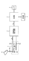
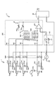
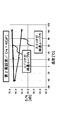
- FIG. 1 is a diagram illustrating an example of a configuration of an input device according to an embodiment of the present invention.
- the input device shown in FIG. 1 includes a sensor unit 1, a capacitance detection device 2, a processing unit 3, a storage unit 4, and an interface unit 5.
- the input device detects a capacitance between an electrode provided on the sensor unit 1 and the object when the object 6 such as a finger or a pen is close to the sensor unit 1. Based on the detection result, information corresponding to the proximity of the object 6 is input. For example, the input device acquires information such as the proximity of the object 6 to the sensor unit 1 and the distance between the sensor unit 1 and the object 6 based on the detection result of the capacitance.
- the input device is applied to a user interface device such as a touch sensor or a touch pad. Note that “proximity” in this specification means being close, and does not limit the presence or absence of contact between adjacent objects.
- the capacitance detection device 2 detects the capacitance of the capacitor Crg formed between the object 6 and the detection electrode Es, and outputs a signal Ds indicating the detection result.
- the interface unit 5 is a circuit for exchanging data between the input device and another device (for example, a host controller of an electronic device equipped with the input device).
- the processing unit 3 obtains information obtained based on the detection result of the capacitance detection device 2 (the presence / absence of the object 6, the proximity position of the object 6, the distance from the object 6, the size of the object 6, etc.) Is output to the host device (not shown) by the interface unit 5.
- a user interface that recognizes, for example, a pointing operation or a gesture operation is constructed using these pieces of information.
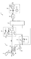
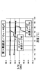
- FIG. 2 is a diagram illustrating an example of the configuration of the capacitance detection device 2 according to the first embodiment.
- the capacitance detection device 2 shown in FIG. 2 outputs a first voltage output circuit 21 that outputs a first AC voltage V1, a second voltage output circuit 22 that outputs a second AC voltage V2, and a drive current Is.
- a current output circuit 23, a subtraction circuit 24, an A / D converter 25, and a signal processing unit 26 are included.
- the capacitance ratio of the first capacitor Ca and the second capacitor Cb is adjusted so that the current I2 flowing through the capacitor Crs (shield electrode side capacitor) and the current I3 flowing through the parasitic capacitor Crgl cancel each other. That is, the capacitance ratio of the first capacitor Ca and the second capacitor Cb has a value adjusted so that the drive current Is in a state where the object 6 close to the detection electrode Es does not exist becomes zero. As shown in Expression (12) described later, when the capacitance ratio between the second capacitor Cb and the first capacitor Ca matches the capacitance ratio between the parasitic capacitor Crgl and the capacitor Crs, the current flowing through the capacitor Crs I2 and current I3 flowing through parasitic capacitor Crgl cancel each other.
- the capacitance value of the first capacitor Ca is constant, and the capacitance value of the second capacitor Cb is adjusted. That is, the second capacitor Cb has a capacitance value adjusted so that the drive current Is in a state where the object 6 close to the detection electrode Es does not exist becomes zero.
- the second capacitor Cb may be a variable-capacitance discrete component or a component formed on a semiconductor chip or the like inside the IC. In the latter case, for example, the second capacitor Cb is composed of a plurality of capacitors connected in parallel, and the capacitance value is adjusted by selecting the number of capacitors connected in parallel by laser trimming or the like.
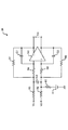
- FIG. 3 is a diagram illustrating an example of the configuration of the subtracting circuit 24.
- the subtraction circuit 24 includes a fully differential amplifier 241, resistors R1 to R7, and capacitors C1 to C3.
- the capacitor C1 is connected between the inverting input terminal and the non-inverting output terminal of the fully differential amplifier 241.
- the capacitor C2 is connected between the non-inverting input terminal and the inverting output terminal of the fully differential amplifier 241.
- the detection signal Vo is input to the inverting input terminal of the fully differential amplifier 241 via the resistors R3 and R4 connected in series.
- the detection signal Vo is input to one end of the resistor R3, and the inverting input terminal of the fully differential amplifier 241 is connected to one end of the resistor R4.
- the A / D converter 25 converts the analog differential signal Vm output from the subtraction circuit 24 into a digital signal Dm.
- a differential input type ⁇ A / D converter can be used as the A / D converter 25.
- the gain of the operational amplifier OP1 When the gain of the operational amplifier OP1 is sufficiently high, the voltage difference between the inverting input terminal and the non-inverting input terminal of the operational amplifier OP1 becomes small, and the voltage at the inverting input terminal of the operational amplifier OP1 is approximately equal to the second AC voltage V2.
- a circuit (a parallel circuit of a feedback capacitor Cag and a feedback resistor Rag in the example of FIG. 2) provided in a path between the output terminal and the inverting input terminal of the operational amplifier OP1 is referred to as a “feedback circuit Zf”. If the impedance is represented by “Zf”, the detection signal Vo is represented by the following equation.
- the detection signal Vo is expressed by the following equation.
- the reference AC voltage corresponding to the AC voltage output as the detection signal Vo from the operational amplifier OP1 in the state where the object 6 close to the detection electrode Es does not exist is generated from the detection signal Vo by the subtraction circuit 24. Subtracted.
- the signal Vm obtained as a result of this subtraction has an amplitude substantially proportional to the capacitance of the capacitor Crg, and becomes minute in a state where the object 6 close to the detection electrode Es does not exist.
- the detection signal Vo has a large amplitude corresponding to the second AC voltage V2 (Equation (9)). Therefore, by providing the subtraction circuit 24, the capacitance of the capacitor Crg can be changed.
- the dynamic range of the corresponding detection signal Vo can be further increased. Therefore, the detection sensitivity of the capacitance of the capacitor Crg can be further increased.
- the operational amplifier OP1, the first resistor Rs, and the feedback capacitor Cag of the current output circuit 23A use a low-pass filter for a signal input from the object 6 via the capacitor Crg. Constitute. Therefore, even if an AC noise voltage is superimposed between the ground where the object 6 is grounded and the ground of the capacitance detection device 2, the noise voltage is attenuated by the low-pass filter of the current output circuit 23A.
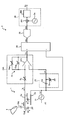
- the electrostatic capacitance detection device 2 detects the electrostatic capacitance for each of the detection electrodes Es1 to Es4.
- the capacitance detection device 2 shown in FIG. 9 has the same configuration (the first voltage output circuit 21, the second voltage output circuit 22, and the subtraction circuit 24) as the capacitance detection device 2 already described, and also has a current output.
- a circuit 23C is included.
- the operational amplifier OP1 amplifies the voltage difference between the inverting input terminal connected to any one of the detection electrodes Es1 to Es4 via the second switch circuit SW2 and the non-inverting input terminal to which the second AC voltage V2 is applied.
- the amplification result is output as a detection signal Vo.
- the feedback circuit Zf is provided in a path between the output terminal of the detection signal Vo of the operational amplifier OP1 and the common node Nc.
- the first switch circuit SW1 selects one input node from the plurality of input nodes N1 to N4 and connects it to the common node Nc.
- the fourth switch circuit SW4 selects an input node not selected by the first switch circuit SW1 and the second switch circuit SW2 from the plurality of input nodes N1 to N4, and applies the first AC voltage V1 to the selected input node. To do. That is, the fourth switch circuit SW4 applies the same first AC voltage V1 as that of the shield electrodes Ea1 to Ea4 to the detection electrode where the capacitance is not detected. As a result, current does not flow to the parasitic capacitor formed between the detection electrode where the capacitance is not detected and the detection electrode to be detected, and the influence of these parasitic capacitors is reduced. Detection sensitivity and detection accuracy are improved.
- the electrostatic capacitance detection device 2 shown in FIG. 12 when the electrostatic capacitance of the detection electrode Esi is detected (the input node Ni is selected in the first switch circuit SW1 and the second switch circuit SW2, and the third switch circuit SW3).
- the connection node NAi is selected in FIG. 7
- the configuration of the current output circuit 23D viewed from the detection electrode Esi is equivalent to the current output circuit 23B in FIG. Accordingly, the gain of the low-pass filter is increased similarly to the capacitance detection device 2 shown in FIG. 7, and the capacitance detection sensitivity is improved.
- the drive current (Is) is output from the operational amplifier (OP1) via the feedback circuit (Zf) provided in the feedback loop of the operational amplifier (OP1), and the voltage from the operational amplifier (OP1) is output.
- the detection signal (Vo) is output, the present invention is not limited to this example.
- the current output circuit may include a current output unit that outputs a current proportional to the drive current, and a current-voltage conversion unit that converts the output current into a voltage and outputs the voltage as a voltage detection signal.
Landscapes
- Engineering & Computer Science (AREA)
- Theoretical Computer Science (AREA)
- General Engineering & Computer Science (AREA)
- Physics & Mathematics (AREA)
- General Physics & Mathematics (AREA)
- Human Computer Interaction (AREA)
- Remote Sensing (AREA)
- Life Sciences & Earth Sciences (AREA)
- Electromagnetism (AREA)
- Power Engineering (AREA)
- Environmental & Geological Engineering (AREA)
- Geology (AREA)
- General Life Sciences & Earth Sciences (AREA)
- Geophysics (AREA)
- Measurement Of Resistance Or Impedance (AREA)
- Electronic Switches (AREA)
- Geophysics And Detection Of Objects (AREA)
Abstract
L'invention concerne un dispositif de détection de capacité (2) comprenant un premier circuit de sortie de tension (21) permettant d'émettre en sortie une première tension (CA V1) fournie à une électrode de blindage (Ea) disposée à proximité d'une électrode de détection (Es), un second circuit de sortie de tension (22) permettant d'émettre en sortie une seconde tension (CA V2) présentant la même fréquence et la même phase que la première tension (CA V1) et une amplitude inférieure à la première tension (CA V1), et un circuit de sortie de courant (23) permettant d'émettre en sortie un courant d'attaque (Is) vers l'électrode de détection (Es) de façon à réduire la différence de tension entre la tension de l'électrode de détection (Es) et la seconde tension (CA V2) et d'émettre en sortie un signal de détection (Vo) correspondant au courant d'attaque (Is). Le second circuit de sortie de tension (22) émet en sortie une seconde tension (CA V2) présentant une amplitude réglée de telle sorte que le courant d'attaque soit nul dans un état dans lequel il n'existe pas d'objet (6) à proximité de l'électrode de détection (Es).
Priority Applications (6)
| Application Number | Priority Date | Filing Date | Title |
|---|---|---|---|
| JP2018557617A JP6667012B2 (ja) | 2016-12-21 | 2017-11-15 | 静電容量検出装置及び入力装置 |
| EP22181439.5A EP4089425B1 (fr) | 2016-12-21 | 2017-11-15 | Dispositif de détection de capacité et dispositif d'entrée |
| EP22181434.6A EP4089424B1 (fr) | 2016-12-21 | 2017-11-15 | Dispositif de détection de capacité et dispositif d'entrée |
| CN201780079128.3A CN110088637B (zh) | 2016-12-21 | 2017-11-15 | 静电电容检测装置以及输入装置 |
| EP17883558.3A EP3561527B1 (fr) | 2016-12-21 | 2017-11-15 | Dispositif de détection de capacité et dispositif d'entrée |
| US16/441,665 US10817114B2 (en) | 2016-12-21 | 2019-06-14 | Capacitance detection device for detecting capacitance between object proximate to detection electrode and the detection electrode and input device used for inputting information according to proximity of object |
Applications Claiming Priority (2)
| Application Number | Priority Date | Filing Date | Title |
|---|---|---|---|
| JP2016247475 | 2016-12-21 | ||
| JP2016-247475 | 2016-12-21 |
Related Child Applications (1)
| Application Number | Title | Priority Date | Filing Date |
|---|---|---|---|
| US16/441,665 Continuation US10817114B2 (en) | 2016-12-21 | 2019-06-14 | Capacitance detection device for detecting capacitance between object proximate to detection electrode and the detection electrode and input device used for inputting information according to proximity of object |
Publications (1)
| Publication Number | Publication Date |
|---|---|
| WO2018116706A1 true WO2018116706A1 (fr) | 2018-06-28 |
Family
ID=62626177
Family Applications (1)
| Application Number | Title | Priority Date | Filing Date |
|---|---|---|---|
| PCT/JP2017/041125 Ceased WO2018116706A1 (fr) | 2016-12-21 | 2017-11-15 | Dispositif de détection de capacité et dispositif d'entrée |
Country Status (5)
| Country | Link |
|---|---|
| US (1) | US10817114B2 (fr) |
| EP (3) | EP4089425B1 (fr) |
| JP (1) | JP6667012B2 (fr) |
| CN (1) | CN110088637B (fr) |
| WO (1) | WO2018116706A1 (fr) |
Cited By (18)
| Publication number | Priority date | Publication date | Assignee | Title |
|---|---|---|---|---|
| WO2020054105A1 (fr) * | 2018-09-14 | 2020-03-19 | アルプスアルパイン株式会社 | Système de détection de proximité |
| WO2020183869A1 (fr) * | 2019-03-12 | 2020-09-17 | アルプスアルパイン株式会社 | Dispositif de détection |
| CN111693784A (zh) * | 2020-07-06 | 2020-09-22 | 北京先通康桥医药科技有限公司 | 一种微弱电容变化测量电路 |
| CN112567895A (zh) * | 2018-08-27 | 2021-03-26 | 塔克托科技有限公司 | 具有嵌入式感测功能的多层结构和相关制造方法 |
| US10990236B2 (en) * | 2019-02-07 | 2021-04-27 | 1004335 Ontario Inc. | Methods for two-touch detection with resistive touch sensor and related apparatuses and systems |
| JPWO2021090636A1 (fr) * | 2019-11-07 | 2021-05-14 | ||
| WO2021225061A1 (fr) * | 2020-05-07 | 2021-11-11 | アルプスアルパイン株式会社 | Dispositif de détection de capacité et dispositif d'entrée |
| JPWO2022038853A1 (fr) * | 2020-08-20 | 2022-02-24 | ||
| JPWO2022074963A1 (fr) * | 2020-10-08 | 2022-04-14 | ||
| WO2022080224A1 (fr) * | 2020-10-14 | 2022-04-21 | アルプスアルパイン株式会社 | Dispositif de détection de capacité électrostatique |
| WO2022168425A1 (fr) * | 2021-02-04 | 2022-08-11 | アルプスアルパイン株式会社 | Dispositif de détection de capacité, procédé de détection de capacité et dispositif d'entrée |
| JPWO2023053488A1 (fr) * | 2021-09-30 | 2023-04-06 | ||
| EP4242807A1 (fr) | 2022-03-09 | 2023-09-13 | Alps Alpine Co., Ltd. | Dispositif de détection de proximité et procédé de détection de survol |
| JP2023542631A (ja) * | 2020-10-15 | 2023-10-11 | アルプスアルパイン株式会社 | 信号の振幅及び位相を制御する方法 |
| WO2023223625A1 (fr) * | 2022-05-16 | 2023-11-23 | アルプスアルパイン株式会社 | Dispositif de détection de capacité |
| KR20240026198A (ko) * | 2021-08-18 | 2024-02-27 | 알프스 알파인 가부시키가이샤 | Dac 발생 구동 쉴드 및 전압 기준 |
| TWI842809B (zh) * | 2019-01-10 | 2024-05-21 | 法商法格爾傳感器公司 | 用於鑑別電容偵測的方法和裝置及配備有此裝置的設備 |
| WO2025047692A1 (fr) * | 2023-08-28 | 2025-03-06 | アルプスアルパイン株式会社 | Capteur capacitif, feuille de capteur, unité de capteur, circuit de détection et dispositif de détection de capacité |
Families Citing this family (25)
| Publication number | Priority date | Publication date | Assignee | Title |
|---|---|---|---|---|
| TWI643113B (zh) * | 2017-03-03 | 2018-12-01 | 日商阿爾普士電氣股份有限公司 | Input device and control method thereof |
| US10976796B2 (en) * | 2017-07-26 | 2021-04-13 | Qualcomm Incorporated | Dynamic range enhancement for self-capacitance measurement |
| JP7009923B2 (ja) * | 2017-10-31 | 2022-01-26 | セイコーエプソン株式会社 | 物理量測定装置、電子機器及び移動体 |
| EP3531143B1 (fr) * | 2017-12-13 | 2022-02-02 | Shenzhen Goodix Technology Co., Ltd. | Procédé de détermination de paramètres de commande pour branche décalée, et dispositif et dispositif de détection tactile associés |
| CN108195490B (zh) * | 2018-01-31 | 2019-10-11 | 北京他山科技有限公司 | 具有分时、分区域屏蔽功能的传感器、电子皮肤和机器人 |
| WO2020059014A1 (fr) * | 2018-09-18 | 2020-03-26 | 国立大学法人東北大学 | Capteur de zone de détection capacitive et dispositif de test de motif conducteur comportant ledit capteur de zone de détection capacitive |
| KR102611016B1 (ko) * | 2018-12-26 | 2023-12-07 | 엘지디스플레이 주식회사 | 터치표시장치 및 그의 구동방법 |
| JP7195443B2 (ja) * | 2019-08-05 | 2022-12-23 | アルプスアルパイン株式会社 | 演算装置、入力装置、演算方法、およびプログラム |
| CN110568961B (zh) * | 2019-09-05 | 2021-04-16 | 合肥松豪电子科技有限公司 | 一种触控面板和应用于触控面板的触摸探测方法 |
| CN110596465B (zh) * | 2019-10-24 | 2022-03-04 | 深圳市汇顶科技股份有限公司 | 电容检测电路、触控装置和终端设备 |
| CN111327734B (zh) * | 2020-01-22 | 2021-07-27 | 维沃移动通信有限公司 | 电子设备及数据传输控制方法 |
| CN111257648A (zh) * | 2020-02-19 | 2020-06-09 | 南京英锐创电子科技有限公司 | 电容检测方法及装置 |
| FR3109437B1 (fr) * | 2020-04-16 | 2022-04-01 | Fogale Nanotech | Dispositif de détection capacitive à électrode déployable, et équipement muni d’un tel dispositif. |
| JP7629255B2 (ja) * | 2020-05-28 | 2025-02-13 | パナソニックオートモーティブシステムズ株式会社 | ステアリング把持センサおよび把持検知方法 |
| CN112014647B (zh) * | 2020-08-10 | 2023-04-28 | 南京天易合芯电子有限公司 | 一种可以抑制温度漂移的电容检测方法 |
| KR102350234B1 (ko) * | 2021-02-13 | 2022-01-12 | 이성호 | 정전용량 검출장치 |
| US20230109442A1 (en) * | 2021-10-01 | 2023-04-06 | Novatek Microelectronics Corp. | Readout circuit and output circuit for reducing resistance |
| KR102775210B1 (ko) * | 2021-11-04 | 2025-03-04 | 주식회사 하이딥 | 터치 장치 및 그 구동 방법 |
| US12254129B2 (en) * | 2022-06-28 | 2025-03-18 | Microsoft Technology Licensing, Llc | Determining charge on a facial-tracking sensor |
| JP7299652B1 (ja) * | 2022-09-27 | 2023-06-28 | 株式会社アトライズヨドガワ | 静電容量センサ |
| US12092672B2 (en) * | 2022-10-12 | 2024-09-17 | Elite Semiconductor Microelectronics Technology Inc. | Capacitance measurement circuit |
| US12326747B1 (en) * | 2022-12-16 | 2025-06-10 | Cadence Design Systems, Inc. | Dual-mode low dropout regulator with fast transient switching between modes |
| US12313664B2 (en) | 2023-08-18 | 2025-05-27 | Elite Semiconductor Microelectronics Technology Inc. | Capacitance measurement circuit |
| TWI850116B (zh) * | 2023-09-21 | 2024-07-21 | 晶豪科技股份有限公司 | 電容量測電路 |
| CN120880427A (zh) * | 2024-04-29 | 2025-10-31 | 兆易创新科技集团股份有限公司 | 缓冲器及集成电路 |
Citations (5)
| Publication number | Priority date | Publication date | Assignee | Title |
|---|---|---|---|---|
| JP2000234939A (ja) * | 1998-12-18 | 2000-08-29 | Yazaki Corp | 静電容量−電圧変換装置 |
| JP2011242370A (ja) * | 2010-05-21 | 2011-12-01 | Renesas Electronics Corp | インピーダンス検出回路及びインピーダンス検出回路の調整方法 |
| JP2015125088A (ja) * | 2013-12-27 | 2015-07-06 | 株式会社村田製作所 | 容量トリミング回路 |
| US9151792B1 (en) * | 2014-05-29 | 2015-10-06 | Cyress Semiconductor Corporation | High-voltage, high-sensitivity self-capacitance sensing |
| WO2016059967A1 (fr) * | 2014-10-15 | 2016-04-21 | アルプス電気株式会社 | Dispositif d'entrée |
Family Cites Families (16)
| Publication number | Priority date | Publication date | Assignee | Title |
|---|---|---|---|---|
| JP3161716B2 (ja) * | 1990-05-21 | 2001-04-25 | 株式会社長野計器製作所 | 容量検出回路 |
| JP4198306B2 (ja) | 1999-07-22 | 2008-12-17 | 東京エレクトロン株式会社 | 静電容量型センサ、半導体製造装置および液晶表示素子製造装置 |
| US6828806B1 (en) | 1999-07-22 | 2004-12-07 | Sumitomo Metal Industries, Ltd. | Electrostatic capacitance sensor, electrostatic capacitance sensor component, object mounting body and object mounting apparatus |
| TW546480B (en) * | 2000-03-07 | 2003-08-11 | Sumitomo Metal Ind | Circuit, apparatus and method for inspecting impedance |
| JP4488400B2 (ja) * | 2001-05-29 | 2010-06-23 | 東京エレクトロン株式会社 | インピーダンス検出回路 |
| DE10333154A1 (de) * | 2003-07-22 | 2005-02-24 | Vega Grieshaber Kg | Verfahren und Schaltungsanordnung zum Auswerten einer Messkapazität |
| US7323886B2 (en) * | 2004-08-16 | 2008-01-29 | Ying Lau Lee | Linear capacitance measurement and touchless switch |
| US20080036473A1 (en) * | 2006-08-09 | 2008-02-14 | Jansson Hakan K | Dual-slope charging relaxation oscillator for measuring capacitance |
| JP4961425B2 (ja) * | 2006-11-30 | 2012-06-27 | パナソニック株式会社 | 演算増幅器 |
| US7818698B2 (en) * | 2007-06-29 | 2010-10-19 | Taiwan Semiconductor Manufacturing Company, Ltd. | Accurate parasitic capacitance extraction for ultra large scale integrated circuits |
| CN101281220B (zh) * | 2008-01-02 | 2010-09-29 | 清华大学 | 电容检测电路及其电容式传感器接口电路芯片 |
| US8222886B2 (en) * | 2008-06-18 | 2012-07-17 | Hioki Denki Kabushiki Kaisha | Voltage detecting apparatus and line voltage detecting apparatus having a detection electrode disposed facing a detected object |
| WO2010013619A1 (fr) * | 2008-07-30 | 2010-02-04 | アルプス電気株式会社 | Dispositif de detection de mouvement a capacite electrostatique et dispositif d’entree dote de ce dispositif de detection |
| CN102221646B (zh) * | 2010-03-15 | 2014-09-24 | 阿尔卑斯电气株式会社 | 电容检测装置和电容检测方法 |
| JP5502597B2 (ja) | 2010-05-24 | 2014-05-28 | ルネサスエレクトロニクス株式会社 | インピーダンス検出回路およびインピーダンス検出方法 |
| WO2013073161A1 (fr) * | 2011-11-15 | 2013-05-23 | 富士電機株式会社 | Circuit de détection de capacité électrostatique |
-
2017
- 2017-11-15 WO PCT/JP2017/041125 patent/WO2018116706A1/fr not_active Ceased
- 2017-11-15 EP EP22181439.5A patent/EP4089425B1/fr active Active
- 2017-11-15 CN CN201780079128.3A patent/CN110088637B/zh active Active
- 2017-11-15 EP EP17883558.3A patent/EP3561527B1/fr active Active
- 2017-11-15 EP EP22181434.6A patent/EP4089424B1/fr active Active
- 2017-11-15 JP JP2018557617A patent/JP6667012B2/ja active Active
-
2019
- 2019-06-14 US US16/441,665 patent/US10817114B2/en active Active
Patent Citations (5)
| Publication number | Priority date | Publication date | Assignee | Title |
|---|---|---|---|---|
| JP2000234939A (ja) * | 1998-12-18 | 2000-08-29 | Yazaki Corp | 静電容量−電圧変換装置 |
| JP2011242370A (ja) * | 2010-05-21 | 2011-12-01 | Renesas Electronics Corp | インピーダンス検出回路及びインピーダンス検出回路の調整方法 |
| JP2015125088A (ja) * | 2013-12-27 | 2015-07-06 | 株式会社村田製作所 | 容量トリミング回路 |
| US9151792B1 (en) * | 2014-05-29 | 2015-10-06 | Cyress Semiconductor Corporation | High-voltage, high-sensitivity self-capacitance sensing |
| WO2016059967A1 (fr) * | 2014-10-15 | 2016-04-21 | アルプス電気株式会社 | Dispositif d'entrée |
Cited By (61)
| Publication number | Priority date | Publication date | Assignee | Title |
|---|---|---|---|---|
| KR20210049093A (ko) * | 2018-08-27 | 2021-05-04 | 택토텍 오와이 | 감지 기능이 내장된 다층 구조체 및 관련된 제조 방법 |
| CN112567895B (zh) * | 2018-08-27 | 2025-07-01 | 塔克托科技有限公司 | 具有嵌入式感测功能的多层结构和相关制造方法 |
| JP2021535463A (ja) * | 2018-08-27 | 2021-12-16 | タクトテック オーイー | 埋め込み検知機能を有する多層構造体および関連製造方法 |
| CN112567895A (zh) * | 2018-08-27 | 2021-03-26 | 塔克托科技有限公司 | 具有嵌入式感测功能的多层结构和相关制造方法 |
| KR102588291B1 (ko) * | 2018-08-27 | 2023-10-11 | 택토텍 오와이 | 감지 기능이 내장된 다층 구조체 및 관련된 제조 방법 |
| US11904455B2 (en) | 2018-09-14 | 2024-02-20 | Alps Alpine Co., Ltd. | Proximity detection system |
| JPWO2020054105A1 (ja) * | 2018-09-14 | 2021-08-30 | アルプスアルパイン株式会社 | 近接検出システム |
| JP7109562B2 (ja) | 2018-09-14 | 2022-07-29 | アルプスアルパイン株式会社 | 近接検出システム |
| WO2020054105A1 (fr) * | 2018-09-14 | 2020-03-19 | アルプスアルパイン株式会社 | Système de détection de proximité |
| TWI842809B (zh) * | 2019-01-10 | 2024-05-21 | 法商法格爾傳感器公司 | 用於鑑別電容偵測的方法和裝置及配備有此裝置的設備 |
| US10990236B2 (en) * | 2019-02-07 | 2021-04-27 | 1004335 Ontario Inc. | Methods for two-touch detection with resistive touch sensor and related apparatuses and systems |
| JP7285311B2 (ja) | 2019-03-12 | 2023-06-01 | アルプスアルパイン株式会社 | 検出装置 |
| CN113396467A (zh) * | 2019-03-12 | 2021-09-14 | 阿尔卑斯阿尔派株式会社 | 检测装置 |
| JPWO2020183869A1 (ja) * | 2019-03-12 | 2021-11-04 | アルプスアルパイン株式会社 | 検出装置 |
| EP3940735A4 (fr) * | 2019-03-12 | 2022-11-23 | Alps Alpine Co., Ltd. | Dispositif de détection |
| US11599222B2 (en) | 2019-03-12 | 2023-03-07 | Alps Alpine Co., Ltd. | Detection device |
| WO2020183869A1 (fr) * | 2019-03-12 | 2020-09-17 | アルプスアルパイン株式会社 | Dispositif de détection |
| WO2021090636A1 (fr) * | 2019-11-07 | 2021-05-14 | アルプスアルパイン株式会社 | Dispositif et procédé de détection de capacité |
| US12019109B2 (en) | 2019-11-07 | 2024-06-25 | Alps Alpine Co., Ltd. | Capacitance detection device and capacitance detection method |
| KR20220061222A (ko) | 2019-11-07 | 2022-05-12 | 알프스 알파인 가부시키가이샤 | 정전 용량 검출 장치 및 정전 용량 검출 방법 |
| KR102711562B1 (ko) * | 2019-11-07 | 2024-09-27 | 알프스 알파인 가부시키가이샤 | 정전 용량 검출 장치 및 정전 용량 검출 방법 |
| US20220244299A1 (en) * | 2019-11-07 | 2022-08-04 | Alps Alpine Co., Ltd. | Capacitance detection device and capacitance detection method |
| JP7170150B2 (ja) | 2019-11-07 | 2022-11-11 | アルプスアルパイン株式会社 | 静電容量検出装置及び静電容量検出方法 |
| JPWO2021090636A1 (fr) * | 2019-11-07 | 2021-05-14 | ||
| US12130986B2 (en) | 2020-05-07 | 2024-10-29 | Alps Alpine Co., Ltd. | Capacitance detection device and input device |
| JPWO2021225061A1 (fr) * | 2020-05-07 | 2021-11-11 | ||
| WO2021225061A1 (fr) * | 2020-05-07 | 2021-11-11 | アルプスアルパイン株式会社 | Dispositif de détection de capacité et dispositif d'entrée |
| DE112021002654T5 (de) | 2020-05-07 | 2023-03-23 | Alps Alpine Co., Ltd. | Kapazitätserfassungsvorrichtung und eingabevorrichtung |
| JP7354432B2 (ja) | 2020-05-07 | 2023-10-02 | アルプスアルパイン株式会社 | 静電容量検出装置及び入力装置 |
| CN111693784A (zh) * | 2020-07-06 | 2020-09-22 | 北京先通康桥医药科技有限公司 | 一种微弱电容变化测量电路 |
| WO2022038853A1 (fr) * | 2020-08-20 | 2022-02-24 | アルプスアルパイン株式会社 | Dispositif et procédé de détection de capacité électrostatique |
| US12174047B2 (en) | 2020-08-20 | 2024-12-24 | Alps Alpine Co., Ltd. | Capacitance detection device and capacitance detection method |
| JP7431335B2 (ja) | 2020-08-20 | 2024-02-14 | アルプスアルパイン株式会社 | 静電容量検出装置、及び、静電容量検出方法 |
| JPWO2022038853A1 (fr) * | 2020-08-20 | 2022-02-24 | ||
| KR20230020520A (ko) * | 2020-08-20 | 2023-02-10 | 알프스 알파인 가부시키가이샤 | 정전 용량 검출 장치, 및, 정전 용량 검출 방법 |
| KR102786037B1 (ko) * | 2020-08-20 | 2025-03-24 | 알프스 알파인 가부시키가이샤 | 정전 용량 검출 장치, 및, 정전 용량 검출 방법 |
| DE112021005309T5 (de) | 2020-10-08 | 2023-07-20 | Alps Alpine Co., Ltd. | Kapzitätserfassungsvorrichtung und eingabevorrichtung |
| JP7406650B2 (ja) | 2020-10-08 | 2023-12-27 | アルプスアルパイン株式会社 | 静電容量検出装置及び入力装置 |
| JPWO2022074963A1 (fr) * | 2020-10-08 | 2022-04-14 | ||
| US11983362B2 (en) | 2020-10-08 | 2024-05-14 | Alps Alpine Co., Ltd. | Capacitance detection device and input device |
| JPWO2022080224A1 (fr) * | 2020-10-14 | 2022-04-21 | ||
| US12590820B2 (en) | 2020-10-14 | 2026-03-31 | Alps Alpine Co., Ltd. | Capacitance detection device |
| WO2022080224A1 (fr) * | 2020-10-14 | 2022-04-21 | アルプスアルパイン株式会社 | Dispositif de détection de capacité électrostatique |
| JP2023542631A (ja) * | 2020-10-15 | 2023-10-11 | アルプスアルパイン株式会社 | 信号の振幅及び位相を制御する方法 |
| JP7559317B2 (ja) | 2020-10-15 | 2024-10-02 | アルプスアルパイン株式会社 | 信号の振幅及び位相を制御する方法 |
| US20230408565A1 (en) * | 2021-02-04 | 2023-12-21 | Alps Alpine Co., Ltd. | Capacitance detection device, capacitance detection method, and input device |
| JP7584545B2 (ja) | 2021-02-04 | 2024-11-15 | アルプスアルパイン株式会社 | 静電容量検出装置、静電容量検出方法及び入力装置 |
| WO2022168425A1 (fr) * | 2021-02-04 | 2022-08-11 | アルプスアルパイン株式会社 | Dispositif de détection de capacité, procédé de détection de capacité et dispositif d'entrée |
| US12385958B2 (en) * | 2021-02-04 | 2025-08-12 | Alps Alpine Co., Ltd. | Capacitance detection device, capacitance detection method, and input device |
| JPWO2022168425A1 (fr) * | 2021-02-04 | 2022-08-11 | ||
| JP7616527B2 (ja) | 2021-08-18 | 2025-01-17 | アルプスアルパイン株式会社 | Dacで生成される駆動シールド及び電圧基準 |
| JP2024529473A (ja) * | 2021-08-18 | 2024-08-06 | アルプスアルパイン株式会社 | Dacで生成される駆動シールド及び電圧基準 |
| KR20240026198A (ko) * | 2021-08-18 | 2024-02-27 | 알프스 알파인 가부시키가이샤 | Dac 발생 구동 쉴드 및 전압 기준 |
| KR102905171B1 (ko) | 2021-08-18 | 2025-12-30 | 알프스 알파인 가부시키가이샤 | Dac 발생 구동 쉴드 및 전압 기준 |
| JP7622961B2 (ja) | 2021-09-30 | 2025-01-28 | アルプスアルパイン株式会社 | 静電容量センサ |
| JPWO2023053488A1 (fr) * | 2021-09-30 | 2023-04-06 | ||
| EP4242807A1 (fr) | 2022-03-09 | 2023-09-13 | Alps Alpine Co., Ltd. | Dispositif de détection de proximité et procédé de détection de survol |
| JPWO2023223625A1 (fr) * | 2022-05-16 | 2023-11-23 | ||
| WO2023223625A1 (fr) * | 2022-05-16 | 2023-11-23 | アルプスアルパイン株式会社 | Dispositif de détection de capacité |
| JP7699719B2 (ja) | 2022-05-16 | 2025-06-27 | アルプスアルパイン株式会社 | 静電容量検出装置 |
| WO2025047692A1 (fr) * | 2023-08-28 | 2025-03-06 | アルプスアルパイン株式会社 | Capteur capacitif, feuille de capteur, unité de capteur, circuit de détection et dispositif de détection de capacité |
Also Published As
| Publication number | Publication date |
|---|---|
| EP4089424B1 (fr) | 2023-09-13 |
| EP4089424A1 (fr) | 2022-11-16 |
| JP6667012B2 (ja) | 2020-03-18 |
| JPWO2018116706A1 (ja) | 2019-10-24 |
| CN110088637B (zh) | 2021-07-27 |
| EP4089425B1 (fr) | 2023-07-12 |
| US10817114B2 (en) | 2020-10-27 |
| EP3561527A4 (fr) | 2020-08-12 |
| EP3561527A1 (fr) | 2019-10-30 |
| CN110088637A (zh) | 2019-08-02 |
| EP4089425A1 (fr) | 2022-11-16 |
| EP3561527B1 (fr) | 2022-08-10 |
| US20190294297A1 (en) | 2019-09-26 |
Similar Documents
| Publication | Publication Date | Title |
|---|---|---|
| JP6667012B2 (ja) | 静電容量検出装置及び入力装置 | |
| JP6357244B2 (ja) | 入力装置 | |
| CN112363003B (zh) | 自电容检测电路、触控芯片和电子设备 | |
| CN110286787B (zh) | 用于触控面板的控制晶片及其运作方法 | |
| CN103339860B (zh) | 电容性近接传感器以及用于电容性近接检测的方法 | |
| JP7170150B2 (ja) | 静電容量検出装置及び静電容量検出方法 | |
| JP6343984B2 (ja) | 非接触電圧計測装置 | |
| TW201635124A (zh) | 高靈敏度的電容觸控裝置及其運作方法 | |
| US20230229261A1 (en) | Capacitance detection device and input device | |
| JP7354432B2 (ja) | 静電容量検出装置及び入力装置 | |
| US10063214B2 (en) | Programmable band-pass filter circuit of analog front-end used for capacitance detection | |
| WO2022109957A1 (fr) | Circuit de détection de capacité propre, puce tactile et dispositif électronique | |
| JP5375680B2 (ja) | 単相差動変換器 | |
| JP7553342B2 (ja) | 増幅回路及び測定装置 | |
| EP3949118B1 (fr) | Suppression de bruit de différentiel | |
| Denisenko et al. | Functional Properties and Frequency Characteristics of Low-Sensitive RC Filters Based on Micropower Operational Amplifiers | |
| Hernández-Jiménez et al. | Bioinstrumentation Amplifier with Band-Pass Differential Filter Using Impedance Converter for Electrocardiography Signals | |
| CN107659289B (zh) | 使用于电容感测之类比前端电路的可程序化带通滤波电路 | |
| TW201635126A (zh) | 高靈敏度的電容觸控裝置及其運作方法 | |
| TW201804728A (zh) | 使用於電容感測之類比前端電路的可程式化帶通濾波電路 | |
| TW201916588A (zh) | 輸入緩衝器及其雜訊消除方法 |
Legal Events
| Date | Code | Title | Description |
|---|---|---|---|
| 121 | Ep: the epo has been informed by wipo that ep was designated in this application |
Ref document number: 17883558 Country of ref document: EP Kind code of ref document: A1 |
|
| ENP | Entry into the national phase |
Ref document number: 2018557617 Country of ref document: JP Kind code of ref document: A |
|
| NENP | Non-entry into the national phase |
Ref country code: DE |
|
| ENP | Entry into the national phase |
Ref document number: 2017883558 Country of ref document: EP Effective date: 20190722 |