WO2018117251A1 - Module laser à semiconducteur et son procédé de production - Google Patents
Module laser à semiconducteur et son procédé de production Download PDFInfo
- Publication number
- WO2018117251A1 WO2018117251A1 PCT/JP2017/046089 JP2017046089W WO2018117251A1 WO 2018117251 A1 WO2018117251 A1 WO 2018117251A1 JP 2017046089 W JP2017046089 W JP 2017046089W WO 2018117251 A1 WO2018117251 A1 WO 2018117251A1
- Authority
- WO
- WIPO (PCT)
- Prior art keywords
- semiconductor laser
- waveguide
- laser module
- semiconductor
- type optical
- Prior art date
- Legal status (The legal status is an assumption and is not a legal conclusion. Google has not performed a legal analysis and makes no representation as to the accuracy of the status listed.)
- Ceased
Links
Images






Classifications
-
- H—ELECTRICITY
- H01—ELECTRIC ELEMENTS
- H01S—DEVICES USING THE PROCESS OF LIGHT AMPLIFICATION BY STIMULATED EMISSION OF RADIATION [LASER] TO AMPLIFY OR GENERATE LIGHT; DEVICES USING STIMULATED EMISSION OF ELECTROMAGNETIC RADIATION IN WAVE RANGES OTHER THAN OPTICAL
- H01S5/00—Semiconductor lasers
- H01S5/02—Structural details or components not essential to laser action
- H01S5/022—Mountings; Housings
- H01S5/023—Mount members, e.g. sub-mount members
- H01S5/02325—Mechanically integrated components on mount members or optical micro-benches
- H01S5/02326—Arrangements for relative positioning of laser diodes and optical components, e.g. grooves in the mount to fix optical fibres or lenses
-
- G—PHYSICS
- G02—OPTICS
- G02B—OPTICAL ELEMENTS, SYSTEMS OR APPARATUS
- G02B6/00—Light guides; Structural details of arrangements comprising light guides and other optical elements, e.g. couplings
- G02B6/24—Coupling light guides
- G02B6/42—Coupling light guides with opto-electronic elements
-
- H—ELECTRICITY
- H01—ELECTRIC ELEMENTS
- H01S—DEVICES USING THE PROCESS OF LIGHT AMPLIFICATION BY STIMULATED EMISSION OF RADIATION [LASER] TO AMPLIFY OR GENERATE LIGHT; DEVICES USING STIMULATED EMISSION OF ELECTROMAGNETIC RADIATION IN WAVE RANGES OTHER THAN OPTICAL
- H01S5/00—Semiconductor lasers
- H01S5/02—Structural details or components not essential to laser action
- H01S5/022—Mountings; Housings
- H01S5/0239—Combinations of electrical or optical elements
-
- H—ELECTRICITY
- H01—ELECTRIC ELEMENTS
- H01S—DEVICES USING THE PROCESS OF LIGHT AMPLIFICATION BY STIMULATED EMISSION OF RADIATION [LASER] TO AMPLIFY OR GENERATE LIGHT; DEVICES USING STIMULATED EMISSION OF ELECTROMAGNETIC RADIATION IN WAVE RANGES OTHER THAN OPTICAL
- H01S5/00—Semiconductor lasers
- H01S5/40—Arrangement of two or more semiconductor lasers, not provided for in groups H01S5/02 - H01S5/30
-
- H—ELECTRICITY
- H01—ELECTRIC ELEMENTS
- H01S—DEVICES USING THE PROCESS OF LIGHT AMPLIFICATION BY STIMULATED EMISSION OF RADIATION [LASER] TO AMPLIFY OR GENERATE LIGHT; DEVICES USING STIMULATED EMISSION OF ELECTROMAGNETIC RADIATION IN WAVE RANGES OTHER THAN OPTICAL
- H01S5/00—Semiconductor lasers
- H01S5/50—Amplifier structures not provided for in groups H01S5/02 - H01S5/30
-
- H—ELECTRICITY
- H01—ELECTRIC ELEMENTS
- H01S—DEVICES USING THE PROCESS OF LIGHT AMPLIFICATION BY STIMULATED EMISSION OF RADIATION [LASER] TO AMPLIFY OR GENERATE LIGHT; DEVICES USING STIMULATED EMISSION OF ELECTROMAGNETIC RADIATION IN WAVE RANGES OTHER THAN OPTICAL
- H01S5/00—Semiconductor lasers
- H01S5/0014—Measuring characteristics or properties thereof
-
- H—ELECTRICITY
- H01—ELECTRIC ELEMENTS
- H01S—DEVICES USING THE PROCESS OF LIGHT AMPLIFICATION BY STIMULATED EMISSION OF RADIATION [LASER] TO AMPLIFY OR GENERATE LIGHT; DEVICES USING STIMULATED EMISSION OF ELECTROMAGNETIC RADIATION IN WAVE RANGES OTHER THAN OPTICAL
- H01S5/00—Semiconductor lasers
- H01S5/005—Optical components external to the laser cavity, specially adapted therefor, e.g. for homogenisation or merging of the beams or for manipulating laser pulses, e.g. pulse shaping
-
- H—ELECTRICITY
- H01—ELECTRIC ELEMENTS
- H01S—DEVICES USING THE PROCESS OF LIGHT AMPLIFICATION BY STIMULATED EMISSION OF RADIATION [LASER] TO AMPLIFY OR GENERATE LIGHT; DEVICES USING STIMULATED EMISSION OF ELECTROMAGNETIC RADIATION IN WAVE RANGES OTHER THAN OPTICAL
- H01S5/00—Semiconductor lasers
- H01S5/005—Optical components external to the laser cavity, specially adapted therefor, e.g. for homogenisation or merging of the beams or for manipulating laser pulses, e.g. pulse shaping
- H01S5/0064—Anti-reflection components, e.g. optical isolators
-
- H—ELECTRICITY
- H01—ELECTRIC ELEMENTS
- H01S—DEVICES USING THE PROCESS OF LIGHT AMPLIFICATION BY STIMULATED EMISSION OF RADIATION [LASER] TO AMPLIFY OR GENERATE LIGHT; DEVICES USING STIMULATED EMISSION OF ELECTROMAGNETIC RADIATION IN WAVE RANGES OTHER THAN OPTICAL
- H01S5/00—Semiconductor lasers
- H01S5/02—Structural details or components not essential to laser action
- H01S5/022—Mountings; Housings
- H01S5/0225—Out-coupling of light
- H01S5/02251—Out-coupling of light using optical fibres
-
- H—ELECTRICITY
- H01—ELECTRIC ELEMENTS
- H01S—DEVICES USING THE PROCESS OF LIGHT AMPLIFICATION BY STIMULATED EMISSION OF RADIATION [LASER] TO AMPLIFY OR GENERATE LIGHT; DEVICES USING STIMULATED EMISSION OF ELECTROMAGNETIC RADIATION IN WAVE RANGES OTHER THAN OPTICAL
- H01S5/00—Semiconductor lasers
- H01S5/02—Structural details or components not essential to laser action
- H01S5/024—Arrangements for thermal management
- H01S5/02407—Active cooling, e.g. the laser temperature is controlled by a thermo-electric cooler or water cooling
- H01S5/02415—Active cooling, e.g. the laser temperature is controlled by a thermo-electric cooler or water cooling by using a thermo-electric cooler [TEC], e.g. Peltier element
-
- H—ELECTRICITY
- H01—ELECTRIC ELEMENTS
- H01S—DEVICES USING THE PROCESS OF LIGHT AMPLIFICATION BY STIMULATED EMISSION OF RADIATION [LASER] TO AMPLIFY OR GENERATE LIGHT; DEVICES USING STIMULATED EMISSION OF ELECTROMAGNETIC RADIATION IN WAVE RANGES OTHER THAN OPTICAL
- H01S5/00—Semiconductor lasers
- H01S5/06—Arrangements for controlling the laser output parameters, e.g. by operating on the active medium
- H01S5/068—Stabilisation of laser output parameters
- H01S5/0683—Stabilisation of laser output parameters by monitoring the optical output parameters
- H01S5/0687—Stabilising the frequency of the laser
-
- H—ELECTRICITY
- H01—ELECTRIC ELEMENTS
- H01S—DEVICES USING THE PROCESS OF LIGHT AMPLIFICATION BY STIMULATED EMISSION OF RADIATION [LASER] TO AMPLIFY OR GENERATE LIGHT; DEVICES USING STIMULATED EMISSION OF ELECTROMAGNETIC RADIATION IN WAVE RANGES OTHER THAN OPTICAL
- H01S5/00—Semiconductor lasers
- H01S5/10—Construction or shape of the optical resonator, e.g. extended or external cavity, coupled cavities, bent-guide, varying width, thickness or composition of the active region
- H01S5/1003—Waveguide having a modified shape along the axis, e.g. branched, curved, tapered, voids
- H01S5/101—Curved waveguide
-
- H—ELECTRICITY
- H01—ELECTRIC ELEMENTS
- H01S—DEVICES USING THE PROCESS OF LIGHT AMPLIFICATION BY STIMULATED EMISSION OF RADIATION [LASER] TO AMPLIFY OR GENERATE LIGHT; DEVICES USING STIMULATED EMISSION OF ELECTROMAGNETIC RADIATION IN WAVE RANGES OTHER THAN OPTICAL
- H01S5/00—Semiconductor lasers
- H01S5/10—Construction or shape of the optical resonator, e.g. extended or external cavity, coupled cavities, bent-guide, varying width, thickness or composition of the active region
- H01S5/1082—Construction or shape of the optical resonator, e.g. extended or external cavity, coupled cavities, bent-guide, varying width, thickness or composition of the active region with a special facet structure, e.g. structured, non planar, oblique
- H01S5/1085—Oblique facets
Definitions
- the present invention relates to a semiconductor laser module and a method for manufacturing the semiconductor laser module.
- a semiconductor laser module used as a light source for optical communication laser light oscillated by a semiconductor laser element (LD) is amplified by a semiconductor optical amplifier (SOA), and the laser light output from the semiconductor laser module is increased.
- SOA semiconductor optical amplifier
- An output configuration is widely adopted.
- integration of the semiconductor laser element and the semiconductor optical amplifier in the same element is also widely adopted (see, for example, Patent Documents 1 to 4).
- thermoelectric element the total power consumption used for adjusting the temperature of the thermoelectric element can be kept low.
- the semiconductor laser element and the semiconductor optical amplifier when adopting a configuration in which the semiconductor laser element and the semiconductor optical amplifier are separated, it is necessary to spatially couple the laser light emitted from the semiconductor laser element to the semiconductor optical amplifier with high accuracy. That is, a new technical problem arises in that the relative alignment between the semiconductor laser element and the semiconductor optical amplifier is accurately performed.
- the problem of alignment in this spatial coupling is not limited to semiconductor optical amplifiers, but includes other optical waveguide elements such as optical modulators, optical waveguide devices made of quartz, silicon, polymers, and the like, and semiconductor laser elements. The same applies to the semiconductor laser module.
- the present invention has been made in view of the above, and an object of the present invention is to provide a semiconductor laser module and a semiconductor laser module capable of accurately performing relative alignment between a semiconductor laser element and a waveguide type optical functional element. It is to provide a manufacturing method.
- a semiconductor laser module includes a semiconductor laser element and a laser beam emitted from the semiconductor laser element that is incident on an incident end to guide the semiconductor laser element.
- a waveguide-type optical functional element having a waveguide to be waved, and a protrusion provided on an extension line of the optical path of the laser light emitted from the semiconductor laser element with respect to the incident end.
- the semiconductor laser module according to an aspect of the present invention further includes a submount to which the waveguide optical functional element is fixed, and the protrusion is fixed on the submount.
- the semiconductor laser module according to one aspect of the present invention is characterized in that the protrusion is fixed on the waveguide type functional element.
- the waveguide of the waveguide type optical functional element has a bending waveguide in the vicinity of the incident end, and the entire waveguide type optical functional element is the semiconductor laser. It is characterized by being disposed obliquely with respect to the optical path of the laser light emitted from the element.
- the semiconductor laser module according to an aspect of the present invention is characterized in that the waveguide type optical functional element is a semiconductor optical amplifier that amplifies the incident laser light.
- the semiconductor laser module according to one aspect of the present invention is characterized in that the protrusion has a hemispherical shape.
- the semiconductor laser module according to one aspect of the present invention is characterized in that the protrusion has a columnar shape.
- the semiconductor laser module according to one aspect of the present invention is characterized in that the protrusion is made of metal.
- the semiconductor laser module according to one aspect of the present invention is characterized in that the protrusion is made of gold (Au).
- a collimator lens and a condenser lens are disposed between the semiconductor laser element and the waveguide type optical functional element, and emitted from the semiconductor laser element.
- the laser beam is spatially coupled to the incident end of the waveguide of the waveguide type optical functional element through the collimating lens and the condenser lens.
- the diameter of the laser beam collimated by the collimator lens is larger than the thickness of the waveguide type optical functional element, and the height of the protrusion related to the submount is high. The height is higher than the height of the waveguide type optical functional element.
- a semiconductor laser module includes a semiconductor laser element and a waveguide type optical functional element having a waveguide that guides laser light emitted from the semiconductor laser element to an incident end. And a submount on which the waveguide-type optical functional element and the protrusion are fixed together, and the protrusion is an extension of the optical path of the laser beam emitted from the semiconductor laser element with respect to the incident end. It is provided on a straight line parallel to.
- a semiconductor laser module manufacturing method includes a semiconductor laser device and a waveguide type optical functional device having a waveguide that guides and guides laser light emitted from the semiconductor laser device.
- a laser element arranging step of fixing the semiconductor laser element to a substrate of the semiconductor laser module, and collimating the laser beam emitted from the semiconductor laser element A collimating lens arrangement step for fixing a collimating lens to the semiconductor laser element, and a projection provided on an extension line in the incident direction from an incident end of the waveguide type optical functional element and the waveguide type optical functional element of the waveguide type optical functional element;
- a laser beam collimated by the collimating lens is applied to the projection by the first submount fixed together with the object.
- the collimating lens arranging step is a step of fixing the collimating lens to a second submount to which the semiconductor laser element is fixed.
- the laser element arranging step is a step of fixing the second submount, to which the semiconductor laser element and the collimating lens are fixed, to the substrate after the collimating lens arranging step.
- the semiconductor laser module and the method for manufacturing the semiconductor laser module according to the present invention have an effect that the relative alignment between the semiconductor laser element and the waveguide type optical functional element can be accurately performed.
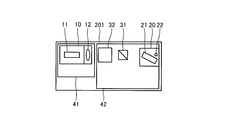
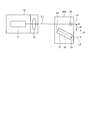
- FIG. 1 is a diagram showing a schematic configuration of the semiconductor laser module according to the first embodiment.
- FIG. 2 is a flowchart showing the gist of the manufacturing method of the semiconductor laser module according to the first embodiment.
- FIG. 3 is a diagram showing a schematic side view configuration of the semiconductor laser module in the positioning step of the semiconductor optical amplifier.
- FIG. 4 is a diagram showing a schematic side configuration of the semiconductor laser module in the step of arranging the condenser lens.
- FIG. 5 is a diagram showing a schematic configuration of the semiconductor laser module according to the second embodiment.
- FIG. 6A is a diagram illustrating a method of putting a substrate into a housing after assembling each component on the substrate.
- FIG. 6A is a diagram illustrating a method of putting a substrate into a housing after assembling each component on the substrate.
- FIG. 6B is a diagram illustrating a method of putting the board into the housing after assembling each component on the board.
- FIG. 6C is a diagram illustrating a method of putting the substrate into the housing after assembling each component on the substrate.
- FIG. 6D is a diagram illustrating a method of putting the substrate into the housing after assembling each component on the substrate.
- FIG. 6E is a diagram illustrating a method of putting the substrate into the housing after assembling each component on the substrate.
- FIG. 6F is a diagram illustrating a method of putting the substrate into the housing after assembling each component on the substrate.
- FIG. 7A is a diagram illustrating a method of sequentially disposing each component on a substrate in the housing.
- FIG. 7B is a diagram illustrating a method of sequentially arranging the components on the substrate in the housing.
- FIG. 7C is a diagram illustrating a method of sequentially disposing each component on the substrate in the housing.
- FIG. 7D is a diagram illustrating a method of sequentially disposing each component on the substrate in the housing.
- FIG. 8 is a diagram for explaining a semiconductor laser module according to the third embodiment.
- FIG. 1 is a diagram showing a schematic configuration of the semiconductor laser module according to the first embodiment.
- the semiconductor laser module according to the first embodiment shown in FIG. 1 shows only a basic configuration, and an actual semiconductor laser module may have various additional configurations as in the embodiments described later.
- the semiconductor laser module 100 includes a semiconductor laser element 11, a semiconductor optical amplifier 21, a protrusion 22, and an SOA submount 20. Further, as shown in FIG. 1, the semiconductor laser module 100 includes a collimating lens 12, a condenser lens 30, and an LD submount 10. These may be configured to be provided on the substrate 101 accommodated in the housing of the semiconductor laser module 100, or may be configured to be provided on the bottom plate using the bottom plate of the housing of the semiconductor laser module 100 as the substrate 101.
- the semiconductor laser element 11 oscillates laser by emitting current and emits laser light.
- a distributed feedback semiconductor laser element that can change the oscillation wavelength by temperature control is used.
- the semiconductor optical amplifier 21 is a representative example of a waveguide-type optical functional element having a waveguide 23 that receives and guides laser light emitted from the semiconductor laser element 11.
- An example is an optical modulator.
- the entire semiconductor optical amplifier 21 is disposed obliquely with respect to the optical path L ⁇ b> 1 of the laser light emitted from the semiconductor laser element 11.
- the waveguide of the semiconductor optical amplifier 21 is formed with a bent waveguide in the vicinity of the incident end 24.
- a bending waveguide is also formed in the vicinity of the emission end 25, and the optical path L2 of the laser light emitted from the semiconductor optical amplifier 21 is substantially parallel to the optical path L1. It is comprised so that.
- Still other examples of the waveguide-type optical functional element having a waveguide include a silica glass-based optical waveguide device such as a planar lightwave circuit (PLC), a silicon waveguide device, and a polymer waveguide device.
- PLC planar lightwave circuit
- the protrusion 22 is a wire ball provided on the extension line L3 related to the incident end 24 of the waveguide of the semiconductor optical amplifier 21 in the optical path L1 of the laser beam emitted from the semiconductor laser element 11.
- the protrusion 22 is a normal wire-bonding hemispherical structure formed of a metal such as gold (Au) for connecting the wiring.
- Au gold
- the protrusion 22 is not used for connecting the wiring but will be described later.
- it is used for positioning (rough adjustment) of the semiconductor optical amplifier 21.
- the protrusion 22 is a wire ball, it can be easily formed because it can be formed in a normal wiring process.
- the protrusion 22 is not limited to a wire ball. Or a structure that can reflect or scatter laser light can be used appropriately.
- the SOA submount 20 is a submount to which the semiconductor optical amplifier 21 and the protrusion 22 are fixed together.
- the height relationship between the semiconductor optical amplifier 21 and the protrusion 22 on the SOA submount 20 is configured such that the height of the protrusion 22 is higher than the height of the semiconductor optical amplifier 21.
- the semiconductor optical amplifier 21 and the protrusion 22 are fixed on the same plane of the SOA submount 20, the height of the protrusion 22 is larger than the thickness of the semiconductor optical amplifier 21.
- the semiconductor optical amplifier 21 has a plate-like shape and has a substantially constant thickness. When the thickness is not constant, the thickness is defined by the thickest portion.
- the protrusion 22 is provided on the extension line L3 related to the incident end 24 of the waveguide of the semiconductor optical amplifier 21 in the optical path L1 of the laser light emitted from the semiconductor laser element 11, and the semiconductor optical amplifier 21
- the relative positional relationship between the protrusion 22 and the protrusion 22 is fixed. Therefore, by positioning the SOA submount 20 with the protrusion 22 as a target, the semiconductor optical amplifier 21 can be positioned as a result.
- the fixing location of the protrusion 22 is not limited on the submount (SOA submount 20).
- the waveguide type optical functional element is fixed on the base together with each optical component, it may be fixed on a thermoelectric element that has been metallized.
- the protrusion is also fixed on the base on which the waveguide device (waveguide type optical functional element) is fixed. Further, when the waveguide included in the waveguide type optical functional element is close to the upper surface of the element, a protrusion may be fixed on the waveguide type optical functional element. In the case of an optical modulator or other waveguide-type optical functional element, since the waveguide is close to the upper surface of the element and the area of the element is large, a protrusion can be fixed on the element.
- the collimating lens 12 is an optical element for collimating the laser light emitted from the semiconductor laser element 11.
- the diameter of the laser beam converted into parallel light by the collimator lens 12 is designed to be larger than the thickness of the semiconductor optical amplifier 21.
- the collimating lens 12 and the semiconductor laser element 11 are disposed on the same LD submount 10.
- the arrangement position of the collimating lens 12 is not limited to this, and may be fixed to the semiconductor laser module 100 independently of the semiconductor laser element 11.
- the collimating lens 12 is not limited to an element independent of the semiconductor laser element 11, and a configuration in which the collimating lens 12 is formed on the emission end face of the semiconductor laser element 11 can be adopted.
- the condensing lens 30 is an optical element for condensing the laser beam collimated by the collimating lens 12 onto the incident end 24 of the waveguide of the semiconductor optical amplifier 21. As will be described later, the condensing lens 30 is disposed during the manufacturing process of the semiconductor laser module. In the state in which the condenser lens 30 is disposed, the laser light in the optical path L1 that has been collimated by the collimator lens 12 is condensed on the incident end 24 of the waveguide of the semiconductor optical amplifier 21, and the waveguide of the semiconductor optical amplifier 21. Then, the light is emitted from the emission end 25 of the semiconductor optical amplifier 21 to the optical path L2.
- the diameter of the laser light collimated by the collimating lens 12 is larger than the thickness of the semiconductor optical amplifier 21, so that part of the laser light traveling along the optical path L1 is a semiconductor It passes through the upper part of the optical amplifier 21 and reaches the protrusion 22 provided on the extension line L3 of the optical path L1 with respect to the incident end 24 of the waveguide of the semiconductor optical amplifier 21.
- the protrusion 22 is a structure that can reflect or scatter laser light such as a wire ball, the laser light that reaches the protrusion 22 is reflected or scattered by the protrusion 22, and the laser light is incident on the protrusion 22. Can be confirmed.
- the SOA submount 20 is positioned so that the projection 22 is irradiated with the laser light collimated by the collimating lens 12 in a state where the condenser lens 30 is not disposed.
- coarse adjustment can be realized such that the laser light emitted from the semiconductor laser element 11 is spatially coupled to the incident end 24 of the waveguide of the semiconductor optical amplifier 21.
- finely adjusting the arrangement of the condenser lens 30 it is possible to realize an arrangement in which the laser light emitted from the semiconductor laser element 11 is appropriately spatially coupled to the incident end 24 of the waveguide of the semiconductor optical amplifier 21. This fine adjustment can be performed while observing the intensity of the laser beam output from the semiconductor optical amplifier 21.
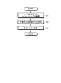
- FIG. 2 is a flowchart showing the gist of the manufacturing method of the semiconductor laser module according to the first embodiment.
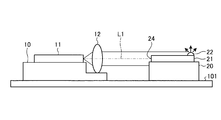
- FIG. 3 is a diagram showing a schematic side view configuration of the semiconductor laser module in the positioning step of the semiconductor optical amplifier.
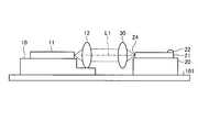
- FIG. 4 is a diagram showing a schematic side configuration of the semiconductor laser module in the step of arranging the condenser lens.
- the manufacturing method of the semiconductor laser module according to the first embodiment starts with a step of arranging the semiconductor laser element 11 and the collimating lens 12 (step S1).
- This step is described as one step in the flowchart shown in FIG. 2, but can be separated into two steps.
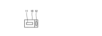
- the collimating lens 12 and the semiconductor laser element 11 are disposed on the same LD submount 10, but the collimating lens 12 is independent of the semiconductor laser element 11. It is also possible to adopt a configuration in which the collimating lens 12 is formed on the emission end face of the semiconductor laser element 11.
- the LD submount is fixed after the collimating lens 12 is fixed to the LD submount 10 to which the semiconductor laser element 11 is fixed.
- the step S1 is realized.
- the collimating lens 12 is automatically formed in the semiconductor. It is fixed to the substrate of the laser module 100, and the step S1 is realized.
- step S1 is implement
- step S2 the positioning process of the semiconductor optical amplifier 21 is performed.
- the description of this step will be referred to here because it will be easier to understand with reference to FIG.
- the positioning process of the semiconductor optical amplifier 21 is performed by fixing the SOA submount 20 to which both the semiconductor optical amplifier 21 and the protrusions 22 prepared in advance are fixed to the substrate 101 of the semiconductor laser module 100.
- the protrusion 22 is provided on the SOA submount 20 on the extension line related to the incident end 24 of the waveguide of the semiconductor optical amplifier 21 in the optical path L1 of the laser light emitted from the semiconductor laser element 11. Yes.
- the diameter of the laser beam converted into parallel light by the collimator lens 12 is designed to be larger than the thickness of the semiconductor optical amplifier 21, and the height of the protrusion 22 is configured to be higher than the height of the semiconductor optical amplifier 21. ing.
- the protrusion 22 is provided on an extension line of the optical path L1 of the laser light emitted from the semiconductor laser element 11 with respect to the incident end 24 of the waveguide of the semiconductor optical amplifier 21, and the relative relationship between the semiconductor optical amplifier 21 and the protrusion 22 is provided. If the fact that the target positional relationship is determined is used, the positioning (coarse adjustment) of the semiconductor optical amplifier 21 can be performed by positioning the SOA submount 20 with the projection 22 as a target.
- step S3 the step of arranging the condenser lens 30 is performed.
- the description of this step will be referred to here because it will be easier to understand with reference to FIG.
- the condenser lens 30 is fixed between the collimating lens 12 and the semiconductor optical amplifier 21.
- the condensing lens 30 is an optical system for condensing the laser light that has been collimated by the collimating lens 12 onto the incident end 24 of the waveguide of the semiconductor optical amplifier 21.
- the arrangement process of the condensing lens 30 is such that the position of the condensing lens 30 is fine so that the laser light collimated by the collimating lens 12 is condensed on the incident end 24 of the waveguide of the semiconductor optical amplifier 21.
- Including the step of adjusting As described above, this fine adjustment can be performed while observing the intensity of the laser beam output from the semiconductor optical amplifier 21.
- the manufacturing method of the semiconductor laser module since the rough adjustment of the position of the semiconductor optical amplifier 21 has been completed in step S2, it is easy to finely adjust the position of the condenser lens 30.
- the relative alignment between the semiconductor laser element 11 and the semiconductor optical amplifier 21 can be accurately performed.
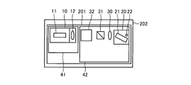
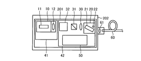
- FIG. 5 is a diagram showing a schematic configuration of the semiconductor laser module according to the second embodiment.
- the configuration of the semiconductor laser module 200 according to the second embodiment shown in FIG. 5 is often the same as that of the first embodiment. Therefore, in the configuration of the semiconductor laser module 200 described below, the same reference numerals as those in the first embodiment are attached, and the description thereof is omitted. It is possible to understand that the configurations and functions of the parts omitted by giving the same reference numerals are substantially the same as those in the first embodiment.
- the semiconductor laser module 200 includes an LD submount 10 that includes a semiconductor laser element 11 and a collimator lens 12, an SOA submount 20 that includes a semiconductor optical amplifier 21 and a protrusion 22, and a condenser lens. 30.
- the configuration of these semiconductor laser modules 200 is substantially the same as that of the first embodiment.
- the LD submount 10 including the semiconductor laser element 11 and the collimator lens 12 is disposed on the LD thermoelectric element 41.
- the LD thermoelectric element 41 is, for example, a Peltier element, and can heat and cool the semiconductor laser element 11 according to the intensity and direction of the current supplied to the LD thermoelectric element 41.
- the semiconductor laser element 11 is, for example, a distributed feedback semiconductor laser element whose oscillation wavelength can be changed by temperature control, and controls the intensity and direction of the current supplied to the LD thermoelectric element 41.
- the wavelength of the laser light emitted from the semiconductor laser element 11 can be controlled.
- the SOA submount 20 including the semiconductor optical amplifier 21 and the protrusions 22 is disposed on the SOA thermoelectric element 42.
- the SOA thermoelectric element 42 is, for example, a Peltier element, and can heat and cool the semiconductor optical amplifier 21 according to the intensity and direction of the current supplied to the SOA thermoelectric element 42. Since the semiconductor optical amplifier 21 is a large heat source, the situation of positive heating is limited. However, in the semiconductor laser module 200 of this configuration, the LD thermoelectric element 41 used for temperature control of the semiconductor laser element 11, the semiconductor Since the SOA thermoelectric element 42 used for temperature control of the optical amplifier 21 is provided independently, it is possible to optimally control the temperature of each of the semiconductor laser element 11 and the semiconductor optical amplifier 21. That is, wasteful power consumption for temperature control of the semiconductor laser element 11 and the semiconductor optical amplifier 21 is reduced, and the total power consumption of the LD thermoelectric element 41 and the SOA thermoelectric element 42 can be kept low.
- the semiconductor laser module 200 includes a first beam splitter 31 and an isolator 32 between the collimating lens 12 and the condenser lens 30.
- the arrangement order of the first beam splitter 31 and the isolator 32 is not limited to that shown in FIG. 5, but the laser beam between the collimator lens 12 and the condenser lens 30 is parallel light. It is preferable to arrange.
- the first beam splitter 31 is an optical element for branching a part of the laser light emitted from the semiconductor laser element 11 to the wavelength locker 50, and is a general branching optical system such as a prism type or a filter type. An element can be used.
- the isolator 32 is an element for preventing laser light that travels backward in the optical path from being incident on the semiconductor laser element 11 due to reflection of the optical element or the like, and laser that travels backward using the polarization of the laser light. It is an optical element that can change only the optical path of light.
- the wavelength locker 50 is a device for measuring the wavelength of the laser beam branched by the first beam splitter 31 and monitoring the wavelength of the laser beam emitted from the semiconductor laser element 11.
- the wavelength of the laser light monitored by the wavelength locker 50 is fed back to the temperature control of the LD thermoelectric element 41, and feedback control is performed so that the semiconductor laser element 11 continues to emit laser light having a desired wavelength.
- the wavelength locker 50 includes a second beam splitter 51, a first light receiving element 52 that directly monitors the intensity of the laser beam branched by the second beam splitter 51, and an intensity of the laser beam branched by the second beam splitter. And a second light receiving element 54 that is monitored via a filter 53.
- the etalon filter 53 is an optical element having periodic transmission characteristics with respect to the wavelength of light. Therefore, it is possible to specify the wavelength of the light by measuring the intensity ratio between the light transmitted through the etalon filter 53 and the light not transmitted.
- the wavelength locker 50 uses the ratio between the intensity of the laser light acquired by the first light receiving element 52 and the intensity of the laser light acquired by the second light receiving element 54, and the wavelength of the laser light branched by the first beam splitter 31. Measure.
- the semiconductor laser module 200 includes an optical fiber 60 that guides the laser light emitted from the semiconductor optical amplifier 21 to the outside of the semiconductor laser module 200, and the semiconductor optical amplifier 21. And a coupling optical system 61 for coupling the laser beam emitted from the optical fiber 60 to the optical fiber 60.
- the coupling optical system 61 shown in FIG. 5 is drawn to be configured by a single lens, but may be configured to be separated into a plurality of components such as a collimating lens and a condensing lens. The positions to be made are not limited to the positions shown in the figure.
- the optical fiber 60 may be a general single-mode glass optical fiber having appropriate propagation characteristics for the laser light emitted from the semiconductor laser element 11.
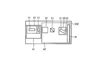
- FIGS. 6A to 6F are diagrams illustrating a method of putting the substrate into the housing after assembling the component components on the substrate.
- FIGS. 7A to 7D are methods of sequentially arranging the component components on the substrate in the housing.
- the LD thermoelectric element 41 and the SOA thermoelectric element 42 are arranged on the substrate 201, the LD submount 10 is arranged on the LD thermoelectric element 41, and the SOA thermoelectric element is arranged.
- a first beam splitter 31 and an isolator 32 are disposed on the surface 42.
- the SOA submount 20 including the semiconductor optical amplifier 21 and the protrusions 22 is fixed to the SOA thermoelectric element 42 while being positioned.
- the positioning method at this time is a method of positioning the semiconductor optical amplifier 21 when the laser beam emitted from the semiconductor laser element 11 and collimated by the collimating lens 12 reaches the protrusion 22. is there.
- the substrate 201 is accommodated in the housing 202. At this time, it is preferable to establish an electrical connection by wiring the components arranged on the substrate 201.
- the condenser lens 30 is arranged.
- the step of arranging the condensing lens 30 includes fine adjustment for condensing the laser light emitted from the semiconductor laser element 11 and collimated by the collimating lens 12 at the incident end of the waveguide of the semiconductor optical amplifier 21. It is out.
- the fine adjustment can be performed by finely adjusting the position of the condenser lens 30 while monitoring the intensity of the laser light output from the semiconductor optical amplifier 21.
- the wavelength locker 50 is attached, and further, the coupling optical system 61 and the optical fiber 60 are attached, and the semiconductor laser module according to the second embodiment is completed.
- the internal configuration of the wavelength locker 50 is as described above.
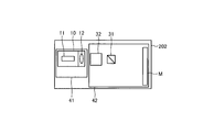
- the LD thermoelectric element 41 and the SOA thermoelectric element 42 are arranged inside the housing 202, and the semiconductor laser element 11 and the collimating lens 12 are placed on the LD thermoelectric element 41.
- the first beam splitter 31 and the isolator 32 are disposed on the SOA thermoelectric element 42.
- an observation mirror M used for positioning work is arranged inside the housing 202.
- the position of the observation mirror M is not limited to the position shown in the figure, and may be arranged at an appropriate position for observing the protrusion during the positioning operation. Further, if it is easy to observe the projection during the positioning operation, the observation mirror M is not necessarily arranged inside the housing 202. Further, another means such as providing an observation window in a part of the housing 202 may be used instead.
- the SOA submount 20 including the semiconductor optical amplifier 21 and the protrusions 22 is fixed to the SOA thermoelectric element 42 while being positioned.
- the positioning method at this time is a method of positioning the semiconductor optical amplifier 21 when the laser beam emitted from the semiconductor laser element 11 and collimated by the collimating lens 12 reaches the protrusion 22. is there.
- the observation mirror M is arranged inside the housing 202, the reflection and scattering of the laser light reaching the protrusion 22 can be easily confirmed.
- the step of arranging the condensing lens 30 includes fine adjustment for condensing the laser light emitted from the semiconductor laser element 11 and collimated by the collimating lens 12 at the incident end of the waveguide of the semiconductor optical amplifier 21. It is out.
- the wavelength locker 50 is attached, and the coupling optical system 61 and the optical fiber 60 are attached, thereby completing the semiconductor laser module according to the second embodiment.
- FIG. 8 a semiconductor laser module according to the third embodiment in which the positions of the protrusions are different will be described with reference to FIG.
- illustration of the substrate and the condenser lens is omitted for the sake of simplicity.
- the extension line L3 is on the SOA submount 20A.
- a protrusion 22 is formed on the straight line L4. The distance D between the extension line L3 and the parallel line L4 is measured in advance.
- the SOA submount 20A After the SOA submount 20A is positioned by the protrusion 22, the SOA submount 20A is shifted upward by the distance D to extend the distance.
- the line L3 and the parallel line L4 are aligned and fixed to the substrate. Thereby, it is possible to easily align the optical path L1 of the laser light emitted from the semiconductor laser element 11 and the incident end 24 of the waveguide of the semiconductor optical amplifier 21.
- the present invention is suitable for application to the field of optical communication, for example.
Landscapes
- Physics & Mathematics (AREA)
- General Physics & Mathematics (AREA)
- Optics & Photonics (AREA)
- Condensed Matter Physics & Semiconductors (AREA)
- Electromagnetism (AREA)
- Semiconductor Lasers (AREA)
- Optical Couplings Of Light Guides (AREA)
Abstract
L'invention concerne un module laser à semiconducteur comprenant : un élément laser à semiconducteur; un élément fonctionnel optique de type guide d'ondes ayant un guide d'ondes qui a, incidente sur celui-ci une lumière laser émise à partir de l'élément laser à semiconducteur et guidant ladite lumière; et un objet en saillie disposé au-dessus d'une ligne d'extension se rapportant à l'extrémité incidente du guide d'ondes dans l'élément fonctionnel optique de type guide d'ondes dans le trajet optique de la lumière laser émise par l'élément laser à semiconducteur. Le module laser à semiconducteur comprend également une embase ayant l'élément fonctionnel optique de type guide d'ondes fixé à celle-ci. L'objet en saillie peut être fixé sur l'embase.
Priority Applications (3)
| Application Number | Priority Date | Filing Date | Title |
|---|---|---|---|
| CN201780079212.5A CN110088994B (zh) | 2016-12-22 | 2017-12-22 | 半导体激光模块和半导体激光模块的制造方法 |
| JP2018558086A JP7166932B2 (ja) | 2016-12-22 | 2017-12-22 | 半導体レーザモジュールおよび半導体レーザモジュールの製造方法 |
| US16/444,778 US11545814B2 (en) | 2016-12-22 | 2019-06-18 | Semiconductor laser module and method of manufacturing semiconductor laser module |
Applications Claiming Priority (2)
| Application Number | Priority Date | Filing Date | Title |
|---|---|---|---|
| JP2016-250076 | 2016-12-22 | ||
| JP2016250076 | 2016-12-22 |
Related Child Applications (1)
| Application Number | Title | Priority Date | Filing Date |
|---|---|---|---|
| US16/444,778 Continuation US11545814B2 (en) | 2016-12-22 | 2019-06-18 | Semiconductor laser module and method of manufacturing semiconductor laser module |
Publications (1)
| Publication Number | Publication Date |
|---|---|
| WO2018117251A1 true WO2018117251A1 (fr) | 2018-06-28 |
Family
ID=62627793
Family Applications (1)
| Application Number | Title | Priority Date | Filing Date |
|---|---|---|---|
| PCT/JP2017/046089 Ceased WO2018117251A1 (fr) | 2016-12-22 | 2017-12-22 | Module laser à semiconducteur et son procédé de production |
Country Status (4)
| Country | Link |
|---|---|
| US (1) | US11545814B2 (fr) |
| JP (1) | JP7166932B2 (fr) |
| CN (1) | CN110088994B (fr) |
| WO (1) | WO2018117251A1 (fr) |
Citations (6)
| Publication number | Priority date | Publication date | Assignee | Title |
|---|---|---|---|---|
| EP1492208A2 (fr) * | 2003-06-27 | 2004-12-29 | NEC Corporation | module laser à semi-conducteur et procédé de son assemblage |
| WO2007108508A1 (fr) * | 2006-03-22 | 2007-09-27 | The Furukawa Electric Co., Ltd. | Module optique |
| WO2010138478A1 (fr) * | 2009-05-26 | 2010-12-02 | Corning Incorporated | Ensemble optique athermique à couplage de proximité comprenant une source laser et un dispositif de conversion de longueur d'onde à facettes composites |
| JP2012164737A (ja) * | 2011-02-04 | 2012-08-30 | Sony Corp | サブマウント、サブマウント組立体及びサブマウント組立方法 |
| WO2013180291A1 (fr) * | 2012-05-31 | 2013-12-05 | 古河電気工業株式会社 | Module de laser à semi-conducteurs |
| US20160013616A1 (en) * | 2014-07-09 | 2016-01-14 | Sumitomo Electric Device Innovations, Inc. | Optical module installing a semiconductor optical amplifier and process to assemble the same |
Family Cites Families (14)
| Publication number | Priority date | Publication date | Assignee | Title |
|---|---|---|---|---|
| FR2287108A1 (fr) * | 1974-10-01 | 1976-04-30 | Radiotechnique Compelec | Dispositif optoelectronique a emetteur et recepteur couples |
| US20040021061A1 (en) * | 2002-07-30 | 2004-02-05 | Frederik Bijkerk | Photodiode, charged-coupled device and method for the production |
| JP4265308B2 (ja) | 2003-06-27 | 2009-05-20 | 日本電気株式会社 | 光学素子ホルダ及びこれを用いた光通信モジュール |
| JP2006216695A (ja) | 2005-02-02 | 2006-08-17 | Furukawa Electric Co Ltd:The | 半導体レーザモジュール |
| JP5008831B2 (ja) | 2005-02-03 | 2012-08-22 | 住友電工デバイス・イノベーション株式会社 | レーザ装置、レーザ装置の制御装置、レーザ装置の制御方法、レーザ装置の波長切換方法およびレーザ装置の制御データ |
| JP2006269846A (ja) | 2005-03-25 | 2006-10-05 | Anritsu Corp | サブマウント及びそれを用いた光半導体装置 |
| JP5104311B2 (ja) | 2005-09-13 | 2012-12-19 | 日本電気株式会社 | 光送信モジュールおよびその製造方法 |
| GB0524217D0 (en) * | 2005-11-28 | 2006-01-04 | Amphotonix Ltd | Fibre-optic module |
| DE102006017293A1 (de) | 2005-12-30 | 2007-07-05 | Osram Opto Semiconductors Gmbh | Verfahren zur Herstellung einer optisch pumpbaren Halbleitervorrichtung |
| JP4913526B2 (ja) | 2006-10-04 | 2012-04-11 | 古河電気工業株式会社 | 光モジュールの製造方法 |
| JP4913527B2 (ja) | 2006-10-04 | 2012-04-11 | 古河電気工業株式会社 | 光モジュールの製造方法、及び、光素子 |
| US9054480B2 (en) | 2009-08-06 | 2015-06-09 | Neophotonics Corporation | Small packaged tunable traveling wave laser assembly |
| JP2016018121A (ja) | 2014-07-09 | 2016-02-01 | 住友電工デバイス・イノベーション株式会社 | 光増幅モジュールを製造する方法 |
| JP6550658B2 (ja) | 2014-07-09 | 2019-07-31 | 住友電工デバイス・イノベーション株式会社 | 光モジュールを製造する方法及び光モジュール |
-
2017
- 2017-12-22 WO PCT/JP2017/046089 patent/WO2018117251A1/fr not_active Ceased
- 2017-12-22 JP JP2018558086A patent/JP7166932B2/ja active Active
- 2017-12-22 CN CN201780079212.5A patent/CN110088994B/zh active Active
-
2019
- 2019-06-18 US US16/444,778 patent/US11545814B2/en active Active
Patent Citations (6)
| Publication number | Priority date | Publication date | Assignee | Title |
|---|---|---|---|---|
| EP1492208A2 (fr) * | 2003-06-27 | 2004-12-29 | NEC Corporation | module laser à semi-conducteur et procédé de son assemblage |
| WO2007108508A1 (fr) * | 2006-03-22 | 2007-09-27 | The Furukawa Electric Co., Ltd. | Module optique |
| WO2010138478A1 (fr) * | 2009-05-26 | 2010-12-02 | Corning Incorporated | Ensemble optique athermique à couplage de proximité comprenant une source laser et un dispositif de conversion de longueur d'onde à facettes composites |
| JP2012164737A (ja) * | 2011-02-04 | 2012-08-30 | Sony Corp | サブマウント、サブマウント組立体及びサブマウント組立方法 |
| WO2013180291A1 (fr) * | 2012-05-31 | 2013-12-05 | 古河電気工業株式会社 | Module de laser à semi-conducteurs |
| US20160013616A1 (en) * | 2014-07-09 | 2016-01-14 | Sumitomo Electric Device Innovations, Inc. | Optical module installing a semiconductor optical amplifier and process to assemble the same |
Also Published As
| Publication number | Publication date |
|---|---|
| US20190312414A1 (en) | 2019-10-10 |
| JPWO2018117251A1 (ja) | 2019-10-31 |
| US11545814B2 (en) | 2023-01-03 |
| CN110088994B (zh) | 2021-03-23 |
| JP7166932B2 (ja) | 2022-11-08 |
| CN110088994A (zh) | 2019-08-02 |
Similar Documents
| Publication | Publication Date | Title |
|---|---|---|
| US8646959B2 (en) | Laser light source | |
| US7275877B2 (en) | Optical module having individual housing for an optical processing unit and an optical sub-assembly | |
| JPH09211272A (ja) | 光モジュール | |
| JP2001339118A (ja) | 発光モジュール | |
| JP2017041618A (ja) | 光モジュール | |
| CN111929776A (zh) | 温控多频道光发射次组件及包含其的收发器模块 | |
| CN107196184A (zh) | 应用壳体、光学部件和移束器的光学模块及其组装方法 | |
| JPWO2007108508A1 (ja) | 光モジュール | |
| JP2011238698A (ja) | レーザモジュール | |
| JP2016045237A (ja) | 発光モジュール及び多チャネル発光モジュール | |
| JPWO2010106978A1 (ja) | 半導体レーザモジュール及び光モジュール | |
| JP6794140B2 (ja) | 光送信機及びこれを含む光モジュール | |
| US20050025420A1 (en) | Optical sub-assembly laser mount having integrated microlens | |
| US11545814B2 (en) | Semiconductor laser module and method of manufacturing semiconductor laser module | |
| JP2012164924A (ja) | 光通信用送信モジュール | |
| US7408867B2 (en) | Method of aligning an optical fiber, method of manufacturing a semiconductor laser module, and semiconductor laser module | |
| US7909518B2 (en) | Optical assembly connecting a laser with optical fibre | |
| JP2008026462A (ja) | 光モジュール | |
| Lin et al. | Grating coupled laser (GCL) for Si photonics | |
| JP6507659B2 (ja) | 光モジュールの製造方法 | |
| JP5837329B2 (ja) | 光半導体装置の製造方法 | |
| JP3956515B2 (ja) | ファイバグレーティング光モジュールの調芯方法 | |
| US20020094590A1 (en) | Method for manufacturing semiconductor laser module, semiconductor laser module and Raman amplifier | |
| WO2002039154A1 (fr) | Module laser a semi-conducteur et amplificateur raman utilisant ledit module | |
| JP2002062458A (ja) | 光モジュールおよびその組立方法、光モジュールを用いた映像表示装置 |
Legal Events
| Date | Code | Title | Description |
|---|---|---|---|
| 121 | Ep: the epo has been informed by wipo that ep was designated in this application |
Ref document number: 17884024 Country of ref document: EP Kind code of ref document: A1 |
|
| ENP | Entry into the national phase |
Ref document number: 2018558086 Country of ref document: JP Kind code of ref document: A |
|
| NENP | Non-entry into the national phase |
Ref country code: DE |
|
| 122 | Ep: pct application non-entry in european phase |
Ref document number: 17884024 Country of ref document: EP Kind code of ref document: A1 |