WO2018123280A1 - Dispositif source de lumière, dispositif d'émission de lumière et dispositif d'affichage - Google Patents
Dispositif source de lumière, dispositif d'émission de lumière et dispositif d'affichage Download PDFInfo
- Publication number
- WO2018123280A1 WO2018123280A1 PCT/JP2017/040229 JP2017040229W WO2018123280A1 WO 2018123280 A1 WO2018123280 A1 WO 2018123280A1 JP 2017040229 W JP2017040229 W JP 2017040229W WO 2018123280 A1 WO2018123280 A1 WO 2018123280A1
- Authority
- WO
- WIPO (PCT)
- Prior art keywords
- terminal
- light emitting
- emitting element
- light
- electrode
- Prior art date
- Legal status (The legal status is an assumption and is not a legal conclusion. Google has not performed a legal analysis and makes no representation as to the accuracy of the status listed.)
- Ceased
Links
Images


Classifications
-
- G—PHYSICS
- G09—EDUCATION; CRYPTOGRAPHY; DISPLAY; ADVERTISING; SEALS
- G09G—ARRANGEMENTS OR CIRCUITS FOR CONTROL OF INDICATING DEVICES USING STATIC MEANS TO PRESENT VARIABLE INFORMATION
- G09G3/00—Control arrangements or circuits, of interest only in connection with visual indicators other than cathode-ray tubes
- G09G3/20—Control arrangements or circuits, of interest only in connection with visual indicators other than cathode-ray tubes for presentation of an assembly of a number of characters, e.g. a page, by composing the assembly by combination of individual elements arranged in a matrix no fixed position being assigned to or needed to be assigned to the individual characters or partial characters
- G09G3/2007—Display of intermediate tones
- G09G3/2014—Display of intermediate tones by modulation of the duration of a single pulse during which the logic level remains constant
-
- G—PHYSICS
- G09—EDUCATION; CRYPTOGRAPHY; DISPLAY; ADVERTISING; SEALS
- G09G—ARRANGEMENTS OR CIRCUITS FOR CONTROL OF INDICATING DEVICES USING STATIC MEANS TO PRESENT VARIABLE INFORMATION
- G09G3/00—Control arrangements or circuits, of interest only in connection with visual indicators other than cathode-ray tubes
- G09G3/20—Control arrangements or circuits, of interest only in connection with visual indicators other than cathode-ray tubes for presentation of an assembly of a number of characters, e.g. a page, by composing the assembly by combination of individual elements arranged in a matrix no fixed position being assigned to or needed to be assigned to the individual characters or partial characters
- G09G3/22—Control arrangements or circuits, of interest only in connection with visual indicators other than cathode-ray tubes for presentation of an assembly of a number of characters, e.g. a page, by composing the assembly by combination of individual elements arranged in a matrix no fixed position being assigned to or needed to be assigned to the individual characters or partial characters using controlled light sources
- G09G3/30—Control arrangements or circuits, of interest only in connection with visual indicators other than cathode-ray tubes for presentation of an assembly of a number of characters, e.g. a page, by composing the assembly by combination of individual elements arranged in a matrix no fixed position being assigned to or needed to be assigned to the individual characters or partial characters using controlled light sources using electroluminescent panels
- G09G3/32—Control arrangements or circuits, of interest only in connection with visual indicators other than cathode-ray tubes for presentation of an assembly of a number of characters, e.g. a page, by composing the assembly by combination of individual elements arranged in a matrix no fixed position being assigned to or needed to be assigned to the individual characters or partial characters using controlled light sources using electroluminescent panels semiconductive, e.g. using light-emitting diodes [LED]
- G09G3/3208—Control arrangements or circuits, of interest only in connection with visual indicators other than cathode-ray tubes for presentation of an assembly of a number of characters, e.g. a page, by composing the assembly by combination of individual elements arranged in a matrix no fixed position being assigned to or needed to be assigned to the individual characters or partial characters using controlled light sources using electroluminescent panels semiconductive, e.g. using light-emitting diodes [LED] organic, e.g. using organic light-emitting diodes [OLED]
- G09G3/3225—Control arrangements or circuits, of interest only in connection with visual indicators other than cathode-ray tubes for presentation of an assembly of a number of characters, e.g. a page, by composing the assembly by combination of individual elements arranged in a matrix no fixed position being assigned to or needed to be assigned to the individual characters or partial characters using controlled light sources using electroluminescent panels semiconductive, e.g. using light-emitting diodes [LED] organic, e.g. using organic light-emitting diodes [OLED] using an active matrix
- G09G3/3233—Control arrangements or circuits, of interest only in connection with visual indicators other than cathode-ray tubes for presentation of an assembly of a number of characters, e.g. a page, by composing the assembly by combination of individual elements arranged in a matrix no fixed position being assigned to or needed to be assigned to the individual characters or partial characters using controlled light sources using electroluminescent panels semiconductive, e.g. using light-emitting diodes [LED] organic, e.g. using organic light-emitting diodes [OLED] using an active matrix with pixel circuitry controlling the current through the light-emitting element
- G09G3/3241—Control arrangements or circuits, of interest only in connection with visual indicators other than cathode-ray tubes for presentation of an assembly of a number of characters, e.g. a page, by composing the assembly by combination of individual elements arranged in a matrix no fixed position being assigned to or needed to be assigned to the individual characters or partial characters using controlled light sources using electroluminescent panels semiconductive, e.g. using light-emitting diodes [LED] organic, e.g. using organic light-emitting diodes [OLED] using an active matrix with pixel circuitry controlling the current through the light-emitting element the current through the light-emitting element being set using a data current provided by the data driver, e.g. by using a two-transistor current mirror
-
- G—PHYSICS
- G09—EDUCATION; CRYPTOGRAPHY; DISPLAY; ADVERTISING; SEALS
- G09G—ARRANGEMENTS OR CIRCUITS FOR CONTROL OF INDICATING DEVICES USING STATIC MEANS TO PRESENT VARIABLE INFORMATION
- G09G3/00—Control arrangements or circuits, of interest only in connection with visual indicators other than cathode-ray tubes
- G09G3/20—Control arrangements or circuits, of interest only in connection with visual indicators other than cathode-ray tubes for presentation of an assembly of a number of characters, e.g. a page, by composing the assembly by combination of individual elements arranged in a matrix no fixed position being assigned to or needed to be assigned to the individual characters or partial characters
- G09G3/34—Control arrangements or circuits, of interest only in connection with visual indicators other than cathode-ray tubes for presentation of an assembly of a number of characters, e.g. a page, by composing the assembly by combination of individual elements arranged in a matrix no fixed position being assigned to or needed to be assigned to the individual characters or partial characters by control of light from an independent source
- G09G3/3406—Control of illumination source
- G09G3/342—Control of illumination source using several illumination sources separately controlled corresponding to different display panel areas, e.g. along one dimension such as lines
- G09G3/3426—Control of illumination source using several illumination sources separately controlled corresponding to different display panel areas, e.g. along one dimension such as lines the different display panel areas being distributed in two dimensions, e.g. matrix
-
- H—ELECTRICITY
- H10—SEMICONDUCTOR DEVICES; ELECTRIC SOLID-STATE DEVICES NOT OTHERWISE PROVIDED FOR
- H10H—INORGANIC LIGHT-EMITTING SEMICONDUCTOR DEVICES HAVING POTENTIAL BARRIERS
- H10H20/00—Individual inorganic light-emitting semiconductor devices having potential barriers, e.g. light-emitting diodes [LED]
- H10H20/80—Constructional details
-
- G—PHYSICS
- G09—EDUCATION; CRYPTOGRAPHY; DISPLAY; ADVERTISING; SEALS
- G09G—ARRANGEMENTS OR CIRCUITS FOR CONTROL OF INDICATING DEVICES USING STATIC MEANS TO PRESENT VARIABLE INFORMATION
- G09G2300/00—Aspects of the constitution of display devices
- G09G2300/04—Structural and physical details of display devices
- G09G2300/0439—Pixel structures
- G09G2300/0452—Details of colour pixel setup, e.g. pixel composed of a red, a blue and two green components
-
- G—PHYSICS
- G09—EDUCATION; CRYPTOGRAPHY; DISPLAY; ADVERTISING; SEALS
- G09G—ARRANGEMENTS OR CIRCUITS FOR CONTROL OF INDICATING DEVICES USING STATIC MEANS TO PRESENT VARIABLE INFORMATION
- G09G2300/00—Aspects of the constitution of display devices
- G09G2300/08—Active matrix structure, i.e. with use of active elements, inclusive of non-linear two terminal elements, in the pixels together with light emitting or modulating elements
- G09G2300/0804—Sub-multiplexed active matrix panel, i.e. wherein one active driving circuit is used at pixel level for multiple image producing elements
-
- G—PHYSICS
- G09—EDUCATION; CRYPTOGRAPHY; DISPLAY; ADVERTISING; SEALS
- G09G—ARRANGEMENTS OR CIRCUITS FOR CONTROL OF INDICATING DEVICES USING STATIC MEANS TO PRESENT VARIABLE INFORMATION
- G09G2300/00—Aspects of the constitution of display devices
- G09G2300/08—Active matrix structure, i.e. with use of active elements, inclusive of non-linear two terminal elements, in the pixels together with light emitting or modulating elements
- G09G2300/0809—Several active elements per pixel in active matrix panels
- G09G2300/0814—Several active elements per pixel in active matrix panels used for selection purposes, e.g. logical AND for partial update
-
- G—PHYSICS
- G09—EDUCATION; CRYPTOGRAPHY; DISPLAY; ADVERTISING; SEALS
- G09G—ARRANGEMENTS OR CIRCUITS FOR CONTROL OF INDICATING DEVICES USING STATIC MEANS TO PRESENT VARIABLE INFORMATION
- G09G2300/00—Aspects of the constitution of display devices
- G09G2300/08—Active matrix structure, i.e. with use of active elements, inclusive of non-linear two terminal elements, in the pixels together with light emitting or modulating elements
- G09G2300/0809—Several active elements per pixel in active matrix panels
- G09G2300/0828—Several active elements per pixel in active matrix panels forming a digital to analog [D/A] conversion circuit
-
- G—PHYSICS
- G09—EDUCATION; CRYPTOGRAPHY; DISPLAY; ADVERTISING; SEALS
- G09G—ARRANGEMENTS OR CIRCUITS FOR CONTROL OF INDICATING DEVICES USING STATIC MEANS TO PRESENT VARIABLE INFORMATION
- G09G2310/00—Command of the display device
- G09G2310/02—Addressing, scanning or driving the display screen or processing steps related thereto
- G09G2310/0264—Details of driving circuits
- G09G2310/0272—Details of drivers for data electrodes, the drivers communicating data to the pixels by means of a current
-
- G—PHYSICS
- G09—EDUCATION; CRYPTOGRAPHY; DISPLAY; ADVERTISING; SEALS
- G09G—ARRANGEMENTS OR CIRCUITS FOR CONTROL OF INDICATING DEVICES USING STATIC MEANS TO PRESENT VARIABLE INFORMATION
- G09G2310/00—Command of the display device
- G09G2310/02—Addressing, scanning or driving the display screen or processing steps related thereto
- G09G2310/0264—Details of driving circuits
- G09G2310/0294—Details of sampling or holding circuits arranged for use in a driver for data electrodes
-
- G—PHYSICS
- G09—EDUCATION; CRYPTOGRAPHY; DISPLAY; ADVERTISING; SEALS
- G09G—ARRANGEMENTS OR CIRCUITS FOR CONTROL OF INDICATING DEVICES USING STATIC MEANS TO PRESENT VARIABLE INFORMATION
- G09G2310/00—Command of the display device
- G09G2310/06—Details of flat display driving waveforms
-
- G—PHYSICS
- G09—EDUCATION; CRYPTOGRAPHY; DISPLAY; ADVERTISING; SEALS
- G09G—ARRANGEMENTS OR CIRCUITS FOR CONTROL OF INDICATING DEVICES USING STATIC MEANS TO PRESENT VARIABLE INFORMATION
- G09G2310/00—Command of the display device
- G09G2310/06—Details of flat display driving waveforms
- G09G2310/066—Waveforms comprising a gently increasing or decreasing portion, e.g. ramp
-
- G—PHYSICS
- G09—EDUCATION; CRYPTOGRAPHY; DISPLAY; ADVERTISING; SEALS
- G09G—ARRANGEMENTS OR CIRCUITS FOR CONTROL OF INDICATING DEVICES USING STATIC MEANS TO PRESENT VARIABLE INFORMATION
- G09G2310/00—Command of the display device
- G09G2310/08—Details of timing specific for flat panels, other than clock recovery
Definitions
- the present disclosure relates to a light source device that emits light of a plurality of colors, a light emitting device having such a light source device, and a display device.
- Patent Document 1 discloses a light emitting diode lighting circuit in which a plurality of light emitting diodes are connected in series.
- Patent Document 2 discloses a display using a plurality of light emitting diodes that can emit light of different colors.
- electronic devices are generally desired to be compact, and light emitting devices are also expected to be compact.
- a light source device includes a first terminal, a second terminal, a third terminal, and a fourth terminal, a first light emitting element, a second light emitting element, and a third terminal.
- the light emitting element is provided.
- the first light emitting element is disposed on the path of the first path from the first terminal to the second terminal, and is connected to the first electrode of the first type and the second terminal.
- a second electrode of the type and emits the first basic color light.
- the second light emitting element is disposed on the path of the second path from the second terminal to the third terminal, and is connected to the second terminal, the first type first electrode, And a second electrode of the type, and emits a second basic color light.
- the third light emitting element is disposed on the path of the third path from the second terminal to the fourth terminal, and is connected to the second terminal, and the first type first electrode, A second electrode of the type and emits a third basic color light.
- a light emitting device includes a first light emitting element, a second light emitting element, a third light emitting element, a first switch, a second switch, and a third switch. , A first current source, a second current source, and a light emission control unit.
- the first light emitting element is disposed on the path of the first path from the first terminal to the second terminal, and is connected to the first electrode of the first type and the second terminal. And a second electrode of the type, and emits the first basic color light.
- the second light emitting element is disposed on the path of the second path from the second terminal to the third terminal, and is connected to the second terminal, the first type first electrode, And a second electrode of the type, and emits a second basic color light.
- the third light emitting element is disposed on the path of the third path from the second terminal to the fourth terminal, and is connected to the second terminal, and the first type first electrode, A second electrode of the type and emits a third basic color light.
- the first switch connects the first terminal and the second terminal by being turned on.
- the second switch connects the second terminal and the third terminal by being turned on.
- the third switch connects the second terminal and the fourth terminal by being turned on.
- the first current source is connected to the third terminal.
- the second current source is connected to the fourth terminal.
- the light emission control unit controls operations of the first switch, the second switch, and the third switch.
- the display device includes a plurality of light emitting devices.
- Each light emitting device includes a first light emitting element, a second light emitting element, a third light emitting element, a first switch, a second switch, a third switch, and a first current source. And a second current source and a light emission control unit.
- the first light emitting element is disposed on the path of the first path from the first terminal to the second terminal, and is connected to the first electrode of the first type and the second terminal. And a second electrode of the type, and emits the first basic color light.
- the second light emitting element is disposed on the path of the second path from the second terminal to the third terminal, and is connected to the second terminal, the first type first electrode, And a second electrode of the type, and emits a second basic color light.
- the third light emitting element is disposed on the path of the third path from the second terminal to the fourth terminal, and is connected to the second terminal, and the first type first electrode, A second electrode of the type and emits a third basic color light.
- the first switch connects the first terminal and the second terminal by being turned on.
- the second switch connects the second terminal and the third terminal by being turned on.
- the third switch connects the second terminal and the fourth terminal by being turned on.
- the first current source is connected to the third terminal.
- the second current source is connected to the fourth terminal.
- the light emission control unit controls operations of the first switch, the second switch, and the third switch.
- the first light emitting element that emits the first basic color light is a route of the first route from the first terminal to the second terminal.
- a second light emitting element that is disposed above and emits the second basic color light is disposed on the second path from the second terminal to the third terminal, and emits the third basic color light.
- the second electrode of the first light emitting element is a second type electrode
- the first electrode of the second light emitting element is a first type electrode
- the first electrode of the third light emitting element is a first type electrode
- the electrode is a first type electrode.
- the second electrode of the first light emitting element, the first electrode of the second light emitting element, and the first electrode of the third light emitting element are connected to the second terminal.
- a compact configuration can be realized.
- the effect described here is not necessarily limited, and there may be any effect described in the present disclosure.
- FIG. 11 is a block diagram illustrating a configuration example of a display device according to an embodiment of the present disclosure.
- FIG. 2 is a circuit diagram illustrating a configuration example of a pixel illustrated in FIG. 1.
- FIG. 3 is a block diagram illustrating a configuration example of a signal generation unit illustrated in FIG. 2.
- FIG. 4 is a timing waveform diagram illustrating an operation example of the signal generation unit illustrated in FIG. 3.
- 3 is a table illustrating an operation example of the pixel illustrated in FIG. 2.
- FIG. 3 is an explanatory diagram illustrating an operation example of the pixel illustrated in FIG. 2.
- FIG. 6 is an explanatory diagram illustrating another operation example of the pixel illustrated in FIG. 2.
- FIG. 6 is an explanatory diagram illustrating another operation example of the pixel illustrated in FIG. 2.
- FIG. 2 is a circuit diagram illustrating a configuration example of a pixel illustrated in FIG. 1.
- FIG. 3 is a block diagram illustrating a configuration example of a signal generation unit illustrated in
- FIG. 6 is an explanatory diagram illustrating another operation example of the pixel illustrated in FIG. 2.
- FIG. 6 is an explanatory diagram illustrating another operation example of the pixel illustrated in FIG. 2.
- FIG. 6 is an explanatory diagram illustrating another operation example of the pixel illustrated in FIG. 2.
- FIG. 3 is a timing waveform diagram illustrating an operation example of the pixel illustrated in FIG. 2. It is a circuit diagram showing one structural example of the pixel which concerns on a comparative example. It is a circuit diagram showing the example of 1 composition of the pixel concerning other comparative examples. It is a circuit diagram showing the example of 1 composition of the pixel concerning other comparative examples. It is a circuit diagram showing the example of 1 structure of the light source part which concerns on a modification.
- FIG. 16 is a circuit diagram illustrating a configuration example of a pixel illustrated in FIG. 15. It is a circuit diagram showing the example of 1 structure of the pixel which concerns on another modification.
- FIG. 18 is a block diagram illustrating a configuration example of a signal generation unit illustrated in FIG. 17.
- FIG. 19 is a timing waveform diagram illustrating an operation example of the signal generation unit illustrated in FIG. 18.
- FIG. 18 is a timing waveform diagram illustrating an operation example of the pixel illustrated in FIG. 17.
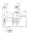
- FIG. 1 illustrates a configuration example of a display device (display device 1) according to an embodiment.
- the display device 1 is a so-called self-luminous display device using a light emitting element as a display element. Note that the light source device and the light emitting device according to the embodiment of the present disclosure are embodied by the present embodiment, and will be described together.
- the display device 1 includes an image signal processing unit 11, a timing control unit 12, a scanning line driving unit 13, a signal line driving unit 14, a control signal generation unit 15, and a display unit 16.
- the image signal processing unit 11 performs predetermined signal processing on an image signal Spic supplied from the outside to generate an image signal Spic2.
- Examples of the predetermined signal processing include gamma correction.
- the timing control unit 12 supplies control signals to the scanning line drive unit 13, the signal line drive unit 14, and the control signal generation unit 15 based on the synchronization signal Ssync supplied from the outside, and these are mutually connected. It controls to operate in synchronization.
- the scanning line driving unit 13 sequentially applies the scanning signal Sscan to a plurality of scanning lines SCL (described later) of the display unit 16 according to the control signal supplied from the timing control unit 12, so that the pixels 20 ( (To be described later) are sequentially selected.
- the signal line drive unit 14 includes a plurality of signals SsigR including the pixel voltage VsigR and a plurality of signals including the pixel voltage VsigG according to the image signal Spic2 supplied from the image signal processing unit 11 and the control signal supplied from the timing control unit 12.
- a plurality of signals SsigB including SsigG and pixel voltage VsigB are generated.
- the signal line driving unit 14 applies a plurality of signals SsigR to a plurality of signal lines SGLR (described later) of the display unit 16, respectively, and applies a plurality of signals SsigG to a plurality of signal lines SGLG (described later).
- the signal SsigB is applied to a plurality of signal lines SGLB (described later) to supply pixel voltages VsigR, VsigG, and VsigB to the pixels 20 selected by the scanning line driving unit 13.
- the control signal generation unit 15 generates a control signal Ssaw having a so-called sawtooth waveform and supplies the control signal Ssaw to each pixel 20 (described later) of the display unit 16.
- the display unit 16 displays an image based on the signals SsigR, SsigG, SsigB, the scanning signal Sscan, and the control signal Ssaw.
- the display unit 16 has a plurality of pixels 20 arranged in a matrix.
- the display unit 16 extends in the column direction, a plurality of scanning lines SCL extending in the row direction (lateral direction in FIG. 1), a plurality of signal lines SGLR extending in the column direction (vertical direction in FIG. 1). It has a plurality of signal lines SGLG and a plurality of signal lines SGLB extending in the column direction.
- One end of the scanning line SCL is connected to the scanning line driving unit 13, and the scanning signal Sscan is applied by the scanning line driving unit 13.
- One ends of the signal lines SGLR, SGLG, and SGLB are connected to the signal line driving unit 14.
- the signal line SGLR is applied with the signal SsigR including the pixel voltage VsigR by the signal line driver 14
- the signal line SGLG is applied with the signal SsigG including the pixel voltage VsigG by the signal line driver 14
- the signal line SGLB is The signal SsigB including the pixel voltage VsigB is applied by the signal line driver 14.
- Each pixel 20 is connected to the scanning line SCL and the three signal lines SGLR, SGLG, SGLB.
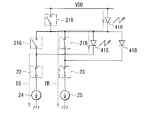
- FIG. 2 shows a configuration example of the pixel 20.
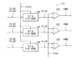
- the pixel 20 includes a light emission control unit 30, transistors 21 ⁇ / b> R, 21 ⁇ / b> G, 21 ⁇ / b> B, 22, 23, current sources 24 and 25, and a light source unit 40.
- the light emission control unit 30, the transistors 21R, 21G, 21B, 22, 23, and the current sources 24, 25 are configured by, for example, one chip (pixel chip).
- the present invention is not limited to this.
- the light source unit 40 is configured by one chip (light source chip).
- the light emission control unit 30 generates signals PWMR, PWMG, PWMB and signals SWG, SWB based on the signals SsigR, SsigG, SsigB, the scanning signal Sscan, and the control signal Ssaw.
- the light emission control unit 30 includes a signal generation unit 31 and OR circuits 34 and 35.
- the signal generator 31 generates signals PWMR, PWMG, and PWMB based on the signals SsigR (pixel voltage VsigR), SsigG (pixel voltage VsigG), SsigB (pixel voltage VsigB), the scanning signal Sscan, and the control signal Ssaw. It is.
- the signal PWMR is a signal having a pulse width PW corresponding to the pixel voltage VsigR
- the signal PWMG is a signal having a pulse width PW corresponding to the pixel voltage VsigG
- the signal PWMB is a pulse width corresponding to the pixel voltage VsigB.
- FIG. 3 shows a configuration example of the signal generation unit 31.
- the signal generator 31 includes sample and hold circuits 32R, 32G, and 32B and comparators 33R, 33G, and 33B.
- the sample hold circuit 32R samples the pixel voltage VsigR included in the signal SsigR based on the scanning signal Sscan, maintains the sampled pixel voltage VsigR, and outputs the pixel voltage VsigR.
- the sample hold circuit 32G samples the pixel voltage VsigG included in the signal SsigG based on the scanning signal Sscan, maintains the sampled pixel voltage VsigG, and outputs the pixel voltage VsigG.
- the sample hold circuit 32B samples the pixel voltage VsigB included in the signal SsigB based on the scanning signal Sscan, maintains the sampled pixel voltage VsigB, and outputs the pixel voltage VsigB.
- the comparator 33R compares the pixel voltage VsigR with the voltage of the control signal Ssaw and outputs the comparison result as a signal PWMR.
- the pixel voltage VsigR is supplied to the positive input terminal of the comparator 33R, and the control signal Ssaw is supplied to the negative input terminal.
- the comparator 33G compares the pixel voltage VsigG with the voltage of the control signal Ssaw and outputs the comparison result as a signal PWMG.
- the pixel voltage VsigG is supplied to the positive input terminal of the comparator 33G, and the control signal Ssaw is supplied to the negative input terminal.
- the comparator 33B compares the pixel voltage VsigB with the voltage of the control signal Ssaw and outputs the comparison result as a signal PWMB.
- the pixel voltage VsigB is supplied to the positive input terminal of the comparator 33B, and the control signal Ssaw is supplied to the negative input terminal.
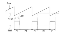
- FIG. 4 shows an operation example of the signal generation unit 31.
- FIG. 4 shows an operation for generating the signal PWMR based on the signal SsigR, the scanning signal Sscan, and the control signal Ssaw.
- the sample hold circuit 32R samples the pixel voltage VsigR included in the signal SsigR and maintains the sampled pixel voltage VsigR. Then, the comparator 33R compares the pixel voltage VsigR with the voltage of the control signal Ssaw. In the period P1 in which the pixel voltage VsigR is higher than the voltage of the control signal Ssaw, the signal PWMR is at a high level, and in the period P2 in which the pixel voltage VsigR is lower than the voltage of the control signal Ssaw, the signal PWMR is at a low level.
- the length (pulse width PW) of the period P1 during which the signal PWMR is at a high level corresponds to the pixel voltage VsigR. That is, the lower the pixel voltage VsigR, the narrower the pulse width PW of the signal PWMR, and the higher the pixel voltage VsigR, the wider the pulse width PW of the signal PWMR.
- the signal generation unit 31 generates the signal PWMR having the pulse width PW corresponding to the pixel voltage VsigR based on the signal SsigR, the scanning signal Sscan, and the control signal Ssaw.
- the signal generator 31 generates a signal PWMG having a pulse width PW corresponding to the pixel voltage VsigG based on the signal SsigG, the scanning signal Sscan, and the control signal Ssaw, and the signal SsigB, the scanning signal Sscan, and the control Based on the signal Ssaw, a signal PWMB having a pulse width PW corresponding to the pixel voltage VsigB is generated.
- the logical sum circuit 34 (FIG. 2) obtains a logical sum (OR) of the signal PWMR and the signal PWMG and outputs the result as a signal SWG.
- the OR circuit 35 calculates a logical sum (OR) of the signal PWMR and the signal PWMB and outputs the result as a signal SWB.
- the transistors 21R, 21G, and 21B are P-type MOS (Metal Oxide Semiconductor) transistors.
- the signal PWMR is supplied to the gate of the transistor 21R, the power supply voltage VDD is supplied to the source, and the drain is connected to the sources of the transistors 21G and 21B and the terminal T2 of the light source unit 40.
- the signal PWMG is supplied to the gate of the transistor 21G, the source is connected to the drain of the transistor 21R, the source of the transistor 21B, and the terminal T2 of the light source unit 40, and the drain is connected to the drain of the transistor 22 and the terminal T3 of the light source unit 40. Connected.
- the signal PWMB is supplied to the gate of the transistor 21B, the source is connected to the drain of the transistor 21R, the source of the transistor 21G, and the terminal T2 of the light source unit 40, and the drain is connected to the drain of the transistor 23 and the terminal T4 of the light source unit 40. Connected.
- the transistors 22 and 23 are N-type MOS transistors.
- a signal SWG is supplied to the gate of the transistor 22, the drain is connected to the drain of the transistor 21 G and the terminal T 3 of the light source unit 40, and the source is connected to one end of the current source 24.
- the signal SWB is supplied to the gate of the transistor 23, the drain is connected to the drain of the transistor 21 B and the terminal T 4 of the light source unit 40, and the source is connected to one end of the current source 25.
- the current source 24 is a so-called constant current source that allows a predetermined current IG to flow from one end to the other end. One end of the current source 24 is connected to the source of the transistor 22, and the other end is grounded.
- the current source 25 is a so-called constant current source that allows a predetermined current IB to flow from one end to the other end. One end of the current source 25 is connected to the source of the transistor 23, and the other end is grounded.
- the light source unit 40 emits red (R), green (G), and blue (B) light.
- the light source unit 40 has four terminals T1 to T4.
- the power supply voltage VDD is supplied to the terminal T1
- the terminal T2 is connected to the drain of the transistor 21R and the sources of the transistors 21G and 21B
- the terminal T3 is connected to the drains of the transistors 21G and 22
- the terminal T4 is connected to the transistors 21B and 23. Connected to the drain.
- the light source unit 40 includes three light emitting elements 41 (light emitting elements 41R, 41G, and 41B).
- the light emitting element 41R emits red (R) light
- the light emitting element 41G emits green (G) light
- the light emitting element 41B emits blue (B) light.
- the light emitting elements 41R, 41G, and 41B can be configured using, for example, light emitting diodes. In addition, it is not limited to this, For example, you may comprise using an organic EL (Electro * Luminescence) element.
- the anode of the light emitting element 41R is connected to the terminal T1, and the cathode is connected to the anode of the light emitting elements 41G and 41B and the terminal T2.
- the anode of the light emitting element 41G is connected to the cathode of the light emitting element 41R, the anode of the light emitting element 41B, and the terminal T2, and the cathode is connected to the terminal T3.
- the anode of the light emitting element 41B is connected to the cathode of the light emitting element 41R, the anode of the light emitting element 41G, and the terminal T2, and the cathode is connected to the terminal T4.
- the light emitting element 41R has a light emitting efficiency lower than that of the light emitting elements 41G and 41B.
- the driving current required for the light emitting element 41R to emit light with a predetermined luminance is larger than the driving current required for the light emitting elements 41G and 41B to emit light with a predetermined luminance.
- the light emitting element 41 (light emitting element 41R in this example) having a low light emission efficiency among the three light emitting elements 41R, 41G, and 41B is disposed on the path from the terminal T1 to the terminal T2.
- the light emitting element 41R and the transistor 21R are connected in parallel. Specifically, the anode of the light emitting element 41R is connected to the source of the transistor 21R, and the cathode of the light emitting element 41R is connected to the drain of the transistor 21R.
- the transistor 21R when the transistor 21R is turned off, a combined current of the currents IG and IB flows through the light emitting element 41R, and the light emitting element 41R emits light.
- the transistor 21R is turned on, a combined current of currents IG and IB flows through the transistor 21R, and the light emitting element 41R is extinguished.
- the light emitting element 41G and the transistor 21G are connected in parallel. Specifically, the anode of the light emitting element 41G is connected to the source of the transistor 21G, and the cathode of the light emitting element 41G is connected to the drain of the transistor 21G.
- the current IG flows through the light emitting element 41G and the light emitting element 41G emits light.
- the transistor 21G is turned on, a current IG flows through the transistor 21G, and the light emitting element 41G is extinguished.
- the light emitting element 41B and the transistor 21B are connected in parallel. Specifically, the anode of the light emitting element 41B is connected to the source of the transistor 21B, and the cathode of the light emitting element 41B is connected to the drain of the transistor 21B.
- the current IB flows through the light emitting element 41B and the light emitting element 41B emits light.
- the transistor 21B is turned on, a current IB flows through the transistor 21B, and the light emitting element 41B is extinguished.
- the light emitting elements 41R, 41G, and 41B are individually driven by pulse width modulation.
- the light emission control unit 30 generates a signal PWMR having a pulse width PW corresponding to the pixel voltage VsigR, a signal PWMG having a pulse width PW corresponding to the pixel voltage VsigG, and a pulse width PW corresponding to the pixel voltage VsigB.
- a signal PWMB is generated.
- the light emitting element 41R emits light according to the signal PWMR
- the light emitting element 41G emits light according to the signal PWMG
- the light emitting element 41B emits light according to the signal PWMB.
- the light emitting element 41R corresponds to a specific example of “first light emitting element” in the present disclosure.
- the light emitting element 41G corresponds to a specific example of “second light emitting element” in the present disclosure.
- the light emitting element 41 ⁇ / b> B corresponds to a specific example of “third light emitting element” in the present disclosure.
- the terminal T1 corresponds to a specific example of “first terminal” in the present disclosure.
- the terminal T2 corresponds to a specific example of “second terminal” in the present disclosure.
- the terminal T3 corresponds to a specific example of “third terminal” in the present disclosure.
- the terminal T4 corresponds to a specific example of “fourth terminal” in the present disclosure.
- the transistor 21R corresponds to a specific example of “first switch” in the present disclosure.
- the transistor 21G corresponds to a specific example of “second switch” in the present disclosure.
- the transistor 21B corresponds to a specific example of “third switch” in the present disclosure.
- the transistor 22 corresponds to a specific example of “fourth switch” in the present disclosure.
- the transistor 23 corresponds to a specific example of “fifth switch” in the present disclosure.
- the current source 24 corresponds to a specific example of “first current source” in the present disclosure.
- the current source 25 corresponds to a specific example of “second current source” in the present disclosure.
- the signal line drive unit 14 corresponds to a specific example of “drive unit” in the present disclosure.
- the image signal processing unit 11 performs predetermined signal processing on the image signal Spic supplied from the outside to generate an image signal Spic2.
- the timing control unit 12 supplies control signals to the scanning line drive unit 13, the signal line drive unit 14, and the control signal generation unit 15 based on the synchronization signal Ssync supplied from the outside, and these are mutually connected. Control to operate synchronously.
- the scanning line driving unit 13 sequentially selects the pixels 20 in units of rows by sequentially applying the scanning signal Sscan to the plurality of scanning lines SCL of the display unit 16 according to the control signal supplied from the timing control unit 12. .
- the signal line drive unit 14 is responsive to the image signal Spic2 supplied from the image signal processing unit 11 and the control signal supplied from the timing control unit 12 to display pixel voltages Vsig (pixel voltages VsigR, VsigG, A plurality of signals Ssig including VsigB) are generated. Then, the signal line driving unit 14 applies the plurality of signals Ssig to the plurality of signal lines SGL of the display unit 16, respectively. Thereby, the signal line driver 14 supplies the pixel voltage Vsig to the pixels 20 selected by the scanning line driver 13.
- the control signal generation unit 15 generates a control signal Ssaw having a so-called sawtooth waveform and supplies the control signal Ssaw to the display unit 16.
- the display unit 16 displays an image based on the signal Ssig, the scanning signal Sscan, and the control signal Ssaw.
- the signal generation unit 31 generates signals PWMR, PWMG, and PWMB based on the signals SsigR, SsigG, SsigB, the scanning signal Sscan, and the control signal Ssaw.
- the transistor 21R is turned on / off based on the signal PWMR
- the transistor 21G is turned on / off based on the signal PWMG
- the transistor 21B is turned on / off based on the signal PWMB.
- the OR circuits 34 and 35 generate signals SWG and SWB based on the signals PWMR, PWMG, and PWMR.
- the transistor 22 is turned on / off based on the signal SWG
- the transistor 23 is turned on / off based on the signal SWB.
- the light emitting elements 41R, 41G, 41B of the light source unit 40 emit or extinguish light based on the on / off state of the transistors 21R, 21G, 21B, 22, 23, respectively.
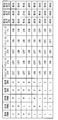
- FIG. 5 shows the operation of the transistors 21R, 21G, 21B and the light emitting elements 41R, 41G, 41B based on the signals PWMR, PWMG, PWMB.
- “H” indicates that the signal is at a high level
- “L” indicates that the signal is at a low level
- “OFF” indicates that the transistor is in an off state
- “ON” indicates that the transistor is in an on state
- “Light emission” indicates that the light emitting element is emitting light
- “Quenching” indicates that the light emitting element is extinguished.
- 6A to 6F schematically show the operation state of the pixel 20.
- the signals PWMR, PWMG, and PWMB are “HHH”
- the signals SWG and SWB are “HH”.
- the transistors 22 and 23 are turned on, and the transistors 21R, 21G, and 21B are turned off.
- the current IG flows in the order of the light emitting element 41R, the light emitting element 41G, the transistor 22, and the current source 24, and the light emitting element 41R, the light emitting element 41B, the transistor 23, and the current source 25 A current IB flows sequentially.
- the total current of the current IG and the current IB flows through the light emitting element 41R, the current IG flows through the light emitting element 41G, and the current IB flows through the light emitting element 41B.
- the light emitting elements 41R, 41G, and 41B each emit light.
- the signals PWMR, PWMG, and PWMB are “HHL”
- the signals SWG and SWB are “HH”.
- the transistors 21B, 22 and 23 are turned on, and the transistors 21R and 21G are turned off.
- the current IG flows in the order of the light emitting element 41R, the light emitting element 41G, the transistor 22, and the current source 24, and the light emitting element 41R, the transistor 21B, the transistor 23, and the current source 25 are in this order.
- a current IB flows.
- the total current of the current IG and the current IB flows through the light emitting element 41R, the current IG flows through the light emitting element 41G, and no current flows through the light emitting element 41B.
- the light emitting elements 41R and 41G emit light, and the light emitting element 41B is quenched.
- the signals PWMR, PWMG, and PWMB are “HLH”, the signals SWG and SWB are “HH”.
- the transistors 21G, 21B, 22, and 23 are turned on, and the transistor 21R is turned off.
- the total current of the current IG and the current IB flows through the light emitting element 41R, the current IB flows through the light emitting element 41B, and no current flows through the light emitting element 41G.
- the light emitting elements 41R and 41B emit light, and the light emitting element 41G is quenched.
- the signals PWMR, PWMG, and PWMB are “HLL”, the signals SWG and SWB are “HH”. Thereby, the transistors 21G, 22, and 23 are turned on, and the transistors 21R and 21B are turned off.
- the current IG flows in the order of the light emitting element 41R, the transistor 21G, the transistor 22, and the current source 24, and the current in the order of the light emitting element 41R, the transistor 21B, the transistor 23, and the current source 25. IB flows. Thereby, the total current of the current IG and the current IB flows through the light emitting element 41R, and no current flows through the light emitting elements 41G and 41B. As a result, the light emitting element 41R emits light, and the light emitting elements 41G and 41B are quenched.
- the signals PWMR, PWMG, and PWMB are “LHH”
- the signals SWG and SWB are “HH”.
- the transistors 21R, 22, and 23 are turned on, and the transistors 21G and 21B are turned off.
- the current IG flows in the order of the transistor 21R, the light emitting element 41G, the transistor 22, and the current source 24, and the current in the order of the transistor 21R, the light emitting element 41B, the transistor 23, and the current source 25.
- IB flows.
- the current IG flows through the light emitting element 41G
- the current IB flows through the light emitting element 41B
- no current flows through the light emitting element 41R As a result, the light emitting elements 41G and 41B each emit light, and the light emitting element 41R is quenched.
- the signals PWMR, PWMG, and PWMB are “LHL”, the signals SWG and SWB are “HL”. Thereby, the transistors 21R, 21B, and 22 are turned on, and the transistors 21G and 23 are turned off.
- the current IG flows in the order of the transistor 21R, the light emitting element 41G, the transistor 22, and the current source 24. Thereby, the current IG flows through the light emitting element 41G, and no current flows through the light emitting elements 41R and 41B. As a result, the light emitting element 41G emits light, and the light emitting elements 41R and 41B are quenched.
- the signals PWMR, PWMG, and PWMB are “LLH”
- the signals SWG and SWB are “LH”. Accordingly, the transistors 21R, 21G, and 23 are turned on, and the transistors 21B and 22 are turned off.
- the current IB flows through the light emitting element 41B, and no current flows through the light emitting elements 41R and 41G. As a result, the light emitting element 41B emits light, and the light emitting elements 41R and 41G are quenched.
- the signals PWMR, PWMG, and PWMB are “LLL”, the signals SWG and SWB are “LL”. Thereby, the transistors 21R, 21G, and 21B are turned on, and the transistors 22 and 23 are turned off. In this case, as shown in FIG. 6F, since no current flows, the light emitting elements 41R, 41G, and 41B are quenched.
- the transistor 21R is turned off, so that a combined current of the currents IG and IB flows through the light emitting element 41R, and the light emitting element 41R emits light.
- the signal PWMG is “H”
- the transistor 21G is turned off, so that the current IG flows through the light emitting element 41G and the light emitting element 41G emits light.
- the transistor 21B is turned off, so that the current IB flows through the light emitting element 41B and the light emitting element 41B emits light.
- the transistor 22 is turned off. That is, in this case, both the transistors 21R and 21G are turned on, and both the light emitting elements 41R and 41G are quenched. Therefore, when both the light emitting elements 41R and 41G are extinguished in this way, the transistor 22 is turned off so that the current IG does not flow, and as a result, power consumption is reduced. Can do.
- the transistor 23 is turned off. That is, in this case, both the transistors 21R and 21B are turned on, and both the light emitting elements 41R and 41B are quenched. Therefore, when both the light emitting elements 41R and 41B are extinguished as described above, the transistor IB is turned off so that the current IB does not flow. As a result, power consumption is reduced. Can do.
- the light emitting elements 41R, 41G, 41B are individually driven based on the signals PWMR, PWMG, PWMB.
- the light emitting elements 41R, 41G, and 41B are individually driven by pulse width modulation.
- the light emission control unit 30 generates a signal PWMR having a pulse width PW corresponding to the pixel voltage VsigR, a signal PWMG having a pulse width PW corresponding to the pixel voltage VsigG, and a pulse width PW corresponding to the pixel voltage VsigB.
- a signal PWMB is generated.
- the light emitting elements 41R, 41G, 41B are individually driven by pulse width modulation based on these signals PWMR, PWMG, PWMB.
- FIG. 7 shows an example of the operation of the pixel 20, where (A) shows the waveform of the signal PWMR, (B) shows the waveform of the signal PWMG, (C) shows the waveform of the signal PWMB, (D) shows the waveform of the signal SWG, (E) shows the waveform of the signal SWB, (F) shows the operation of the light emitting element 41R, (G) shows the operation of the light emitting element 41G, and (H) shows the light emission. The operation of the element 41B is shown. 7F to 7H, white indicates that the light emitting element emits light, and black indicates that the light emitting element is quenched.
- the signal generation unit 31 of the light emission control unit 30 changes the signal PWMR from a low level to a high level, changes the signal PWMG from a low level to a high level, and changes the signal PWMB from a low level to a high level.
- the level is changed (FIGS. 7A to 7C).
- the OR circuit 34 of the light emission control unit 30 changes the signal SWG from the low level to the high level according to the transition of the signals PWMR and PWMG, and the OR circuit 35 responds to the transition of the signals PWMR and PWMB.
- the signal SWB is transited from the low level to the high level (FIGS. 7D and 7E). Accordingly, the light emitting elements 41R, 41G, and 41B emit light during the period of timing t1 to t2 (FIGS. 7F to 7H).
- the signal generator 31 causes the signal PWMB to transition from a high level to a low level (FIG. 7C).
- the light emitting elements 41R and 41G emit light, and the light emitting element 41B is extinguished (FIGS. 7F to 7H).
- the signal generator 31 makes the signal PWMR transition from a high level to a low level (FIG. 7A). Further, the OR circuit 35 makes the signal SWB transition from the high level to the low level in response to the transition of the signal PWMR (FIG. 7E). Thus, in the period from timing t3 to t4, the light emitting element 41G emits light, and the light emitting elements 41R and 41B are extinguished (FIGS. 7F to 7H).
- the signal generation unit 31 causes the signal PWMG to transition from a high level to a low level (FIG. 7B). Further, the OR circuit 34 changes the signal SWG from the high level to the low level in accordance with the transition of the signal PWMG (FIG. 7D). Accordingly, the light emitting elements 41R, 41G, and 41B are extinguished during the period from the timing t4 to t5 (FIGS. 7F to 7H).
- the light emitting elements 41R, 41G, and 41B are individually driven by pulse width modulation based on the signals PWMR, PWMG, and PWMB.
- the light source unit 40 in the light source unit 40, four terminals T1 to T4 are provided, a light emitting element 41R is provided on a path from the terminal T1 to the terminal T2, and the terminal T2 to the terminal T3 is provided.
- the light emitting element 41G is provided on the path, and the light emitting element 41B is provided on the path from the terminal T2 to the terminal T4.
- the light source chip (light source unit 40) and the pixel chip are arranged. Wiring can be simplified, and as a result, the pixel 20 can be made compact.
- the resolution of the display device 1 can be increased, and the image quality can be improved.
- the parasitic capacitance of the wiring between the light source chip (light source unit 40) and the pixel chip can be reduced, the light emitting elements 41R, 41G, and 41B can be driven at a high operating speed. Can improve image quality.
- the transistor 22 since the transistor 22 is provided and the light emitting elements 41R and 41G do not emit light, the transistor 22 is turned off, so that power consumption can be reduced.
- the transistor 23 when the transistor 23 is provided and the light emitting elements 41R and 41B do not emit light, the transistor 23 is turned off, so that power consumption can be reduced.
- the light emitting element 41 (light emitting element 41R in this example) having a low light emission efficiency among the light emitting elements 41R, 41G, and 41B is disposed on the path from the terminal T1 to the terminal T2. Therefore, the image quality of the display device 1 can be improved. That is, since the total current generated by the two current sources 24 and 25 flows in the path from the terminal T1 to the terminal T2, the light emitting element 41 is arranged on the path from the terminal T1 to the terminal T2. Emits light with higher luminance than when the light emitting element 41 is arranged on another path.
- the length of the light emitting period of the light emitting element 41 when the light emitting element 41 is arranged on the path from the terminal T1 to the terminal T2 is the length of the light emitting period when the light emitting element 41 is arranged on another path. Shorter than length.
- the length of the light emitting period of the light emitting element 41 is further shortened. For example, when the length of the light emission period is extremely short, the light emitting element 41 may not be able to emit light appropriately. In this case, the image quality of the display device 1 may be deteriorated.
- the light emitting element 41 (light emitting element 41 ⁇ / b> R in this example) of the light emitting elements 41 ⁇ / b> R, 41 ⁇ / b> G, 41 ⁇ / b> B is disposed on the path from the terminal T ⁇ b> 1 to the terminal T ⁇ b> 2. Since the length of the light emission period of the light emitting element 41 arranged on the path from the terminal T2 to the terminal T2 can be ensured, the image quality of the display device 1 can be improved.
- FIG. 8 illustrates a configuration example of the pixel 50 of the display device 5 according to the first comparative example.
- the pixel 50 includes a light emission control unit 51, transistors 52 R, 52 G, 52 B, 53 to 55, current sources 56 to 58, and a light source unit 59.
- the light emission control unit 51 generates signals PWMR, PWMG, PWMB and signals SWR, SWG, SWB based on the signals SsigR, SsigG, SsigB, the scanning signal Sscan, and the control signal Ssaw.
- the transistors 52R, 52G, and 52B are P-type MOS transistors.
- the signal PWMR is supplied to the gate of the transistor 52R, the power supply voltage VDD is supplied to the source, and the drain is connected to the drain of the transistor 53 and the terminal T14 of the light source unit 59.
- the signal PWMG is supplied to the gate of the transistor 52G, the power supply voltage VDD is supplied to the source, and the drain is connected to the drain of the transistor 54 and the terminal T15 of the light source unit 59.
- the signal PWMB is supplied to the gate of the transistor 52B, the power supply voltage VDD is supplied to the source, and the drain is connected to the drain of the transistor 55 and the terminal T16 of the light source unit 59.
- the transistors 53 to 55 are N-type MOS transistors.
- the signal SWR is supplied to the gate of the transistor 53, the drain is connected to the drain of the transistor 52 R and the terminal T 14 of the light source unit 59, and the source is connected to one end of the current source 56.
- a signal SWG is supplied to the gate of the transistor 54, the drain is connected to the drain of the transistor 52 G and the terminal T 15 of the light source unit 59, and the source is connected to one end of the current source 57.
- the signal SWB is supplied to the gate of the transistor 55, the drain is connected to the drain of the transistor 52 B and the terminal T 16 of the light source unit 59, and the source is connected to one end of the current source 58.
- the current source 56 is a so-called constant current source that allows a predetermined current IR to flow from one end to the other end. One end is connected to the source of the transistor 53 and the other end is grounded.
- the current source 57 is a so-called constant current source that allows a predetermined current IG to flow from one end to the other end. One end is connected to the source of the transistor 54 and the other end is grounded.
- the current source 58 is a so-called constant current source that allows a predetermined current IB to flow from one end to the other end. One end is connected to the source of the transistor 55 and the other end is grounded.
- the light source unit 59 has six terminals T11 to T16.
- the power supply voltage VDD is supplied to the terminals T11 to T13, the terminal T14 is connected to the drains of the transistors 52R and 53, the terminal T15 is connected to the drains of the transistors 52G and 54, and the terminal T16 is connected to the drains of the transistors 52B and 55. Is done.
- the light source unit 59 includes three light emitting elements 59R, 59G, and 59B.
- the anode of the light emitting element 59R is connected to the terminal T11, and the cathode is connected to the terminal T14.
- the anode of the light emitting element 59G is connected to the terminal T12, and the cathode is connected to the terminal T15.
- the anode of the light emitting element 59B is connected to the terminal T13, and the cathode is connected to the terminal T16.
- the light source unit 59 is composed of one chip (light source chip).
- the three current sources 56, 57, and 58 are provided corresponding to the three light emitting elements 59R, 59G, and 59B, power consumption may increase. Further, since the light source unit 59 has the six terminals T11 to T16, the wiring between the light source chip and the pixel chip may be complicated.
- the display device 1 since only two current sources 24 and 25 are required, power consumption can be suppressed. Further, in the display device 1, since the number of terminals of the light source unit 40 is four, wiring between the light source chip and the pixel chip can be simplified, and the pixel 20 can be made compact. As a result, the display device 1 can improve image quality, for example, as described above.
- FIG. 9 illustrates a configuration example of the pixel 60 of the display device 6 according to the second comparative example.
- the pixel 60 has a function equivalent to two pixels.
- the pixel 60 includes a light emission control unit 61, transistors 62R, 62G, and 62B, and a light source unit 69.
- the light emission control unit 61 generates signals PWMR1, PWMG1, PWMB1, signals PWMR2, PWMG2, PWMB2, and signals SWR, SWG, SWB based on the signals SsigR, SsigG, SsigB, the scanning signal Sscan, and the control signal Ssaw. To do.
- the light emission control unit 61 samples the pixel voltage VsigR1 included in the signal SsigR, the pixel voltage VsigG1 included in the signal SsigG, and the pixel voltage VsigB1 included in the signal SsigB based on the scanning signal Sscan, Based on the voltages VsigR1, VsigG1, VsigB1 and the control signal Ssaw, a signal PWMR1 having a pulse width PW corresponding to the pixel voltage VsigR1, a signal PWMG1 having a pulse width PW corresponding to the pixel voltage VsigG1, and a pulse corresponding to the pixel voltage VsigB1 A signal PWMB1 having a width PW is generated.
- the light emission control unit 61 samples the pixel voltage VsigR2 included in the signal SsigR, the pixel voltage VsigG2 included in the signal SsigG, and the pixel voltage VsigB2 included in the signal SsigB based on the scanning signal Sscan. Based on VsigG2, VsigB2 and the control signal Ssaw, a signal PWMR2 having a pulse width PW corresponding to the pixel voltage VsigR2, a signal PWMG2 having a pulse width PW corresponding to the pixel voltage VsigG2, and a pulse width PW corresponding to the pixel voltage VsigB2 are obtained. A signal PWMB2 is generated.
- the signal PWMR1 is supplied to the gate of the transistor 52R, and the drain is connected to the source of the transistor 62R, the terminal T14 of the light source unit 59, and the terminal T21 of the light source unit 69.
- a signal PWMG1 is supplied to the gate of the transistor 52G, and the drain is connected to the source of the transistor 62G, the terminal T15 of the light source unit 59, and the terminal T22 of the light source unit 69.
- the signal PWMB1 is supplied to the gate of the transistor 52B, and the drain is connected to the source of the transistor 62B, the terminal T16 of the light source unit 59, and the terminal T23 of the light source unit 69.
- Transistors 62R, 62G, and 62B are P-type MOS transistors.
- a signal PWMR2 is supplied to the gate of the transistor 62R, the source is connected to the drain of the transistor 52R, the terminal T14 of the light source unit 59, and the terminal T21 of the light source unit 69, and the drain is the drain of the transistor 53 and the terminal of the light source unit 69.
- the signal PWMG2 is supplied to the gate of the transistor 62G, the source is connected to the drain of the transistor 52G, the terminal T15 of the light source unit 59, and the terminal T22 of the light source unit 69, and the drain is the drain of the transistor 54 and the terminal of the light source unit 69. Connected to T25.
- the signal PWMB2 is supplied to the gate of the transistor 62B, the source is connected to the drain of the transistor 52B, the terminal T16 of the light source unit 59, and the terminal T23 of the light source unit 69, and the drain is the drain of the transistor 55 and the terminal of the light source unit 69. Connected to T26.
- the drain of the transistor 53 is connected to the drain of the transistor 62R and the terminal T24 of the light source unit 69.
- the drain of the transistor 54 is connected to the drain of the transistor 62G and the terminal T25 of the light source unit 69.
- the drain of the transistor 55 is connected to the drain of the transistor 62B and the terminal T26 of the light source unit 69.
- the terminal T14 of the light source unit 59 is connected to the drain of the transistor 52R, the source of the transistor 62R, and the terminal T21 of the light source unit 69, and the terminal T15 is the drain of the transistor 52G, the source of the transistor 62G, and the terminal T22 of the light source unit 69.
- the terminal T16 is connected to the drain of the transistor 52B, the source of the transistor 62B, and the terminal T23 of the light source unit 69.
- the light source unit 69 has six terminals T21 to T26.
- the terminal T21 is connected to the drain of the transistor 52R, the source of the transistor 62R, and the terminal T14 of the light source unit 59.
- the terminal T22 is connected to the drain of the transistor 52G, the source of the transistor 62G, and the terminal T15 of the light source unit 59.
- the terminal T23 is connected to the drain of the transistor 52B, the source of the transistor 62B, and the terminal T16 of the light source unit 59.
- the terminal T24 is connected to the drains of the transistors 62R and 53, the terminal T25 is connected to the drains of the transistors 62G and 54, and the terminal T26 is connected to the drains of the transistors 62B and 55.
- the light source unit 69 includes three light emitting elements 69R, 69G, and 69B.
- the anode of the light emitting element 69R is connected to the terminal T21, and the cathode is connected to the terminal T24.
- the anode of the light emitting element 69G is connected to the terminal T22, and the cathode is connected to the terminal T25.
- the anode of the light emitting element 69B is connected to the terminal T23, and the cathode is connected to the terminal T26.
- the light source unit 69 is composed of one chip (light source chip).
- the light source units 59 and 69 each have six terminals, wiring between the two light source chips and wiring between each light source chip and the pixel chip are complicated. There is a fear. Further, for example, when a so-called open failure occurs in the path from the terminal T11 to the terminal T14 of the light source unit 59 corresponding to the first pixel, the light emitting element 69R of the light source unit 69 corresponding to the second pixel is changed. There is a possibility that the light cannot be emitted.
- the display device 1 since the number of terminals of the light source unit 40 is four, the wiring between the light source chip and the pixel chip can be simplified, and the pixel 20 is made compact. be able to. As a result, the display device 1 can improve image quality, for example, as described above. In addition, since the display device 1 has an independent configuration for each pixel, even if, for example, an open failure occurs in a certain pixel, the risk of affecting other pixels can be reduced.
- FIG. 10 illustrates a configuration example of the pixel 70 of the display device 7 according to the third comparative example.
- the pixel 70 includes a light emission control unit 71, transistors 72 R, 72 G, 72 B, 73 to 75, current sources 76 to 78, and a light source unit 79.
- the light emission control unit 71 generates signals PWMR, PWMG, PWMB and signals SWR1, SWG1, SWB1 based on the signals SsigR, SsigG, SsigB, the scanning signal Sscan, and the control signal Ssaw.
- Transistors 72R, 72G, and 72B are P-type MOS transistors.
- the signal PWMR is supplied to the gate of the transistor 72R, the power supply voltage VDD is supplied to the source, and the drain is connected to the source of the transistor 72G, the drain of the transistor 73, and the terminal T32 of the light source unit 79.
- the signal PWMG is supplied to the gate of the transistor 72G, the source is connected to the drains of the transistors 72R and 73 and the terminal T32 of the light source unit 79, and the drains are the source of the transistor 72B, the drain of the transistor 74, and the terminal of the light source unit 79. Connected to T33.
- the signal PWMB is supplied to the gate of the transistor 72B, the source is connected to the drains of the transistors 72G and 74 and the terminal T33 of the light source unit 79, and the drain is connected to the drain of the transistor 75 and the terminal T34 of the light source unit 79.
- Transistors 73 to 75 are N-type MOS transistors.
- a signal SWR1 is supplied to the gate of the transistor 73, the drain is connected to the drain of the transistor 72R, the source of the transistor 72G, and the terminal T32 of the light source unit 79, and the source is connected to one end of the current source 77.
- a signal SWG1 is supplied to the gate of the transistor 74, the drain is connected to the drain of the transistor 72G, the source of the transistor 72B, and the terminal T33 of the light source unit 79, and the source is connected to one end of the current source 77.
- a signal SWB 1 is supplied to the gate of the transistor 75, the drain is connected to the drain of the transistor 72 B and the terminal T 34 of the light source unit 79, and the source is connected to one end of the current source 78.
- the current source 78 is a so-called constant current source that allows a predetermined current IB to flow from one end to the other end. One end of the current source 78 is connected to the source of the transistor 75, and the other end is grounded.
- the light source unit 79 has four terminals T31 to T34.
- the terminal T31 is supplied with the power supply voltage VDD
- the terminal T32 is connected to the drains of the transistors 72R and 73 and the source of the transistor 72G
- the terminal T33 is connected to the drains of the transistors 72G and 74 and the source of the transistor 72B
- the terminal T34 is The drains of the transistors 72B and 75 are connected.
- the light source unit 79 includes three light emitting elements 79R, 79G, and 79B.
- the anode of the light emitting element 79R is connected to the terminal T31
- the cathode is connected to the anode of the light emitting element 79G and the terminal T32.
- the anode of the light emitting element 79G is connected to the cathode of the light emitting element 79R and the terminal T32, and the cathode is connected to the anode of the light emitting element 79B and the terminal T33.
- the anode of the light emitting element 79B is connected to the cathode of the light emitting element 79G and the terminal T33, and the cathode is connected to the terminal T34.
- the light source unit 79 is composed of one chip (light source chip).
- the power supply voltage VDD may have to be increased.
- the light emitting element 41R is provided on the path from the terminal T1 to the terminal T2, and the light emitting element 41G is provided on the path from the terminal T2 to the terminal T3.
- the light emitting element 41B is provided on the path from the terminal T2 to the terminal T4.
- one light emitting element 41R is provided on the path from the terminal T1 to the terminal T2
- one light emitting element 41G is provided on the path from the terminal T2 to the terminal T3, and the path from the terminal T2 to the terminal T4.
- one light emitting element 41B is provided above, the present invention is not limited to this. Instead, a plurality of (three in this example) light emitting elements are provided on the path from the terminal T1 to the terminal T2, as in the light source unit 40A shown in FIG. 11, and the path from the terminal T2 to the terminal T3.
- a plurality (three in this example) of light emitting elements may be provided on the top, and a plurality (three in this example) of light emitting elements may be provided on the path from the terminal T2 to the terminal T4.
- three light emitting elements 41R, 42R, and 43R connected in series are arranged on the path from the terminal T1 to the terminal T2, and 3 connected in series on the path from the terminal T2 to the terminal T3.
- Two light emitting elements 41G, 42G, 43G are arranged, and three light emitting elements 41B, 42B, 43B connected in series are arranged on the path from the terminal T2 to the terminal T4.
- the same number of light emitting elements are provided on the three paths, but the present invention is not limited to this. Instead, the number of light emitting elements in each path may not be equal to each other, for example, as in the light source unit 40B illustrated in FIG.
- two light emitting elements 41R and 42R connected in series are arranged on the path from the terminal T1 to the terminal T2, and three light emitting elements connected in series are arranged on the path from the terminal T2 to the terminal T3.
- Elements 41G, 42G, and 43G are arranged, and three light emitting elements 41B, 42B, and 43B connected in series are arranged on a path from the terminal T2 to the terminal T4.
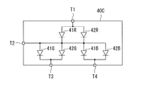
- a plurality of light emitting elements are connected in series in each path, but the present invention is not limited to this. Instead, for example, a plurality of (two in this example) light emitting elements connected in parallel are provided on the path from the terminal T1 to the terminal T2 as in the light source unit 40C shown in FIG. A plurality of (two in this example) light emitting elements connected in parallel are provided on the path from the terminal T3 to the terminal T3, and a plurality of (two in this example) connected in parallel on the path from the terminal T2 to the terminal T4. May be provided.
- two light emitting elements 41R and 42R connected in parallel are arranged on the path from the terminal T1 to the terminal T2, and two light emitting elements connected in parallel on the path from the terminal T2 to the terminal T3 are arranged.
- Elements 41G and 42G are arranged, and two light emitting elements 41B and 42B connected in parallel are arranged on the path from the terminal T2 to the terminal T4.
- the number of light emitting elements in each path may not be equal to each other.
- two light emitting elements 41R and 42R connected in parallel are arranged on the path from the terminal T1 to the terminal T2, and one light emitting element 41G is arranged on the path from the terminal T2 to the terminal T3.
- One light emitting element 41B is arranged on the path from the terminal T2 to the terminal T4.
- the light source unit 40 includes the light emitting element 41R that emits red (R) light, the light emitting element 41G that emits green (G) light, and the light emitting element 41B that emits blue (B) light.
- the light emitting element 41R that emits red (R) light
- the light emitting element 41G that emits green (G) light
- the light emitting element 41B that emits blue (B) light.
- a light emitting element that emits yellow or white color may be provided.
- the display device 1E provided with the yellow (Y) light emitting element 41Y will be described in detail.
- FIG. 15 illustrates a configuration example of the display device 1E.
- the display device 1E includes an image signal processing unit 11E, a signal line driving unit 14E, and a display unit 16E.
- the image signal processing unit 11E performs predetermined signal processing on the image signal Spic supplied from the outside to generate an image signal Spic3.
- the image signal processing unit 11E has a function of converting luminance information of three colors (red, green, and blue) into luminance information of four colors (red, green, blue, and yellow).
- the signal line drive unit 14E according to the image signal Spic3 supplied from the image signal processing unit 11E and the control signal supplied from the timing control unit 12, a plurality of signals SsigR including the pixel voltage VsigR and a plurality of signals including the pixel voltage VsigG.
- a plurality of signals SsigB including SsigG, a pixel voltage VsigB, and a plurality of signals SsigY including the pixel voltage VsigY are generated.
- the signal line driving unit 14E applies the plurality of signals SsigR to the plurality of signal lines SGLR of the display unit 16E, applies the plurality of signals SsigG to the plurality of signal lines SGLG, and supplies the plurality of signals SsigB to the plurality of signals SsigB.
- the pixel voltages VsigR, VsigG, VsigB, and VsigY are applied to the pixels 80 selected by the scanning line driving unit 13 by applying the signals to the signal lines SGLB and applying the plurality of signals SsigY to the plurality of signal lines SGLY (described later), respectively. To supply.
- the display unit 16E displays an image based on the signals SsigR, SsigG, SsigB, SsigY, the scanning signal Sscan, and the control signal Ssaw.
- the display unit 16E has a plurality of pixels 80 arranged in a matrix.
- the display unit 16E extends in the column direction, a plurality of scanning lines SCL extending in the row direction (lateral direction in FIG. 1), a plurality of signal lines SGLR extending in the column direction (vertical direction in FIG. 1). It has a plurality of signal lines SGLG, a plurality of signal lines SGLB extending in the column direction, and a plurality of signal lines SGLY extending in the column direction.
- One ends of the signal lines SGLR, SGLG, SGLB, and SGLY are connected to the signal line driving unit 14E.
- the signal line SGLR is applied with the signal SsigR including the pixel voltage VsigR by the signal line driver 14E
- the signal line SGLG is applied with the signal SsigG including the pixel voltage VsigG by the signal line driver 14E
- the signal line SGLB is
- the signal SsigB including the pixel voltage VsigB is applied by the signal line driver 14E
- the signal SsigY including the pixel voltage VsigY is applied to the signal line SGLY by the signal line driver 14E.
- Each pixel 80 is connected to the scanning line SCL and the four signal lines SGLR, SGLG, SGLB, SGLY.
- FIG. 16 shows a configuration example of the pixel 80.
- the pixel 80 includes a light emission control unit 30E, transistors 21Y and 84, a current source 86, and a light source unit 40E.
- the light source unit 40E is configured by one chip (light source chip).
- the light emission control unit 30E generates signals PWMR, PWMG, PWMB, and PWMY and signals SWG, SWB, and SWY based on the signals SsigR, SsigG, SsigB, SsigY, the scanning signal Sscan, and the control signal Ssaw. .
- the light emission control unit 30E includes a signal generation unit 31E and an OR circuit 36.
- the signal generator 31E PWMG, PWMB, and PWMY are generated.
- the signal PWMY is a signal having a pulse width PW corresponding to the pixel voltage VsigY.
- the OR circuit 36 calculates a logical sum (OR) of the signal PWMR and the signal PWMY, and outputs the result as a signal SWY.
- the transistor 21Y is a P-type MOS transistor.
- the signal PWMY is supplied to the gate of the transistor 21Y, the source is connected to the drain of the transistor 21R, the sources of the transistors 21G and 21B, and the terminal T2 of the light source unit 40E, and the drain is the drain of the transistor 84 and the terminal of the light source unit 40E. Connected to T5.
- the transistor 84 is an N-type MOS transistor.
- the signal SWY is supplied to the gate of the transistor 84, the drain is connected to the drain of the transistor 21Y and the terminal T5 of the light source unit 40E, and the source is connected to one end of the current source 86.
- the current source 86 is a so-called constant current source that allows a predetermined current IY to flow from one end to the other end.
- One end of the current source 86 is connected to the source of the transistor 84, and the other end is grounded.
- the light source unit 40E emits red (R), green (G), blue (B), and yellow (Y) light.
- the light source unit 40E has five terminals T1 to T5.
- the terminal T5 is connected to the drains of the transistors 21Y and 84.
- the light source unit 40E includes four light emitting elements 41 (light emitting elements 41R, 41G, 41B, and 41Y).
- the light emitting element 41Y emits yellow (Y) light.
- the light emitting element 41Y can be configured using, for example, a light emitting element that emits blue (B) light and a phosphor that converts the blue light into yellow (Y) light.
- the anode of the light emitting element 41Y is connected to the cathode of the light emitting element 41R, the anodes of the light emitting elements 41G and 41B, and the terminal T2, and the cathode is connected to the terminal T5.
- FIG. 17 illustrates a configuration example of the pixel 120 of the display device 1F.
- the pixel 120 includes a light emission control unit 130, current sources 124 and 125, transistors 121R, 121G, 121B, 122, and 123, and a light source unit 140.
- the light source unit 140 is configured by one chip (light source chip).
- the light emission controller 130 generates signals PWMR, PWMG, PWMB and signals SWG, SWB based on the signals SsigR, SsigG, SsigB, the scanning signal Sscan, and the control signal Ssaw.
- the light emission control unit 130 includes a signal generation unit 131 and AND circuits 134 and 135.
- the signal generator 131 generates signals PWMR, PWMG, and PWMB based on the signals SsigR (pixel voltage VsigR), SsigG (pixel voltage VsigG), SsigB (pixel voltage VsigB), the scanning signal Sscan, and the control signal Ssaw. It is.
- FIG. 18 shows a configuration example of the signal generation unit 131.
- the signal generation unit 131 includes comparators 33R, 33G, and 33B.
- the control signal Ssaw is supplied to the positive input terminal of the comparator 33R, and the pixel voltage VsigR is supplied to the negative input terminal.
- the control signal Ssaw is supplied to the positive input terminal of the comparator 33G, and the pixel voltage VsigG is supplied to the negative input terminal.
- the control signal Ssaw is supplied to the positive input terminal of the comparator 33B, and the pixel voltage VsigB is supplied to the negative input terminal.
- FIG. 19 shows an operation example of the signal generation unit 131.
- the comparator 33R compares the pixel voltage VsigR with the voltage of the control signal Ssaw. In the period P11 in which the pixel voltage VsigR is higher than the voltage of the control signal Ssaw, the signal PWMR becomes low level, and in the period P12 in which the pixel voltage VsigR is lower than the voltage of the control signal Ssaw, the signal PWMR becomes high level.
- the length (pulse width PW) of the period P11 during which the signal PWMR is at a low level corresponds to the pixel voltage VsigR. That is, the lower the pixel voltage VsigR, the narrower the pulse width PW of the signal PWMR, and the higher the pixel voltage VsigR, the wider the pulse width PW of the signal PWMR.
- the AND circuit 134 (FIG. 17) obtains a logical product (AND) of the signal PWMR and the signal PWMG and outputs the result as a signal SWG.
- the AND circuit 135 calculates a logical product (AND) of the signal PWMR and the signal PWMB and outputs the result as a signal SWB.
- the current source 124 is a so-called constant current source that allows a predetermined current IG to flow from one end to the other end.
- the power supply voltage VDD is supplied to one end of the current source 124, and the other end is connected to the source of the transistor 122.
- the current source 125 is a so-called constant current source that allows a predetermined current IB to flow from one end to the other end.
- the power supply voltage VDD is supplied to one end of the current source 125, and the other end is connected to the source of the transistor 123.
- the transistors 122 and 123 are P-type MOS transistors.
- the signal SWG is supplied to the gate of the transistor 122, the source is connected to the other end of the current source 124, and the drain is connected to the drain of the transistor 121G and the terminal T3 of the light source unit 140.
- the signal SWB is supplied to the gate of the transistor 123, the source is connected to the other end of the current source 125, and the drain is connected to the drain of the transistor 121B and the terminal T4 of the light source unit 140.
- the transistors 121R, 121G, and 121B are N-type MOS transistors.
- the signal PWMG is supplied to the gate of the transistor 121G, the drain is connected to the drain of the transistor 122 and the terminal T3 of the light source unit 140, and the source is connected to the source of the transistor 121B, the drain of the transistor 121R, and the terminal T2 of the light source unit 140.
- the signal PWMB is supplied to the gate of the transistor 121B, the drain is connected to the drain of the transistor 123 and the terminal T4 of the light source unit 140, and the source is connected to the source of the transistor 121G, the drain of the transistor 121R, and the terminal T2 of the light source unit 140.
- the signal PWMR is supplied to the gate of the transistor 121R, the drain is connected to the sources of the transistors 121G and 121B and the terminal T2 of the light source unit 140, and the source is grounded.
- the terminal T3 of the light source unit 140 is connected to the drains of the transistors 122 and 121G, the terminal T4 is connected to the drains of the transistors 123 and 121B, the terminal T2 is connected to the sources of the transistors 121G and 121B and the drain of the transistor 121R, and the terminal T1. Is grounded.
- the anode of the light emitting element 41G is connected to the terminal T3, and the cathode is connected to the cathode of the light emitting element 41B, the anode of the light emitting element 41R, and the terminal T2.
- the anode of the light emitting element 41B is connected to the terminal T4, and the cathode is connected to the cathode of the light emitting element 41G, the anode of the light emitting element 41R, and the terminal T2.
- the anode of the light emitting element 41R is connected to the cathodes of the light emitting elements 41G and 41B and the terminal T2, and the cathode is connected to the terminal T1.
- the light emitting element 41R has a light emitting efficiency lower than that of the light emitting elements 41G and 41B.
- FIG. 20 shows an operation example of the pixel 120.
- the signal generation unit 131 of the light emission control unit 130 changes the signal PWMR from a high level to a low level, changes the signal PWMG from a high level to a low level, and changes the signal PWMB from a high level to a low level.
- the level is changed (FIGS. 20A to 20C).
- the AND circuit 134 of the light emission control unit 130 changes the signal SWG from a high level to a low level in response to the transition of the signals PWMR and PWMG, and the AND circuit 135 changes in response to the transition of the signals PWMR and PWMB.
- the signal SWB is shifted from the high level to the low level (FIGS. 20D and 20E).
- the light emitting elements 41R, 41G, and 41B emit light during the period from the timing t11 to t12 (FIGS. 20G to 20H).
- the signal generation unit 131 causes the signal PWMB to transition from a low level to a high level (FIG. 20C).
- the light emitting elements 41R and 41G emit light, and the light emitting element 41B is quenched (FIGS. 20G to 20H).
- the signal generation unit 131 causes the signal PWMR to transition from a low level to a high level (FIG. 20A). Further, the logical product circuit 135 causes the signal SWB to transition from the low level to the high level in response to the transition of the signal PWMR (FIG. 20E).
- the light emitting element 41G emits light, and the light emitting elements 41R and 41B are extinguished (FIGS. 20G to 20H).
- the signal generation unit 131 causes the signal PWMG to transition from a low level to a high level (FIG. 20B). Further, the logical product circuit 134 causes the signal SWG to transition from the low level to the high level in response to the transition of the signal PWMG (FIG. 20D). Thus, the light emitting elements 41R, 41G, and 41B are extinguished during the period from the timing t14 to t15 (FIGS. 20G to 20H).
- the light emitting element 41R that emits red light is provided on the path from the terminal T1 to the terminal T2, and the light emitting element 41G that emits green light is provided on the path from the terminal T2 to the terminal T3.
- the light emitting element 41B that emits blue light is provided on the path from the terminal T2 to the terminal T4.
- the present invention is not limited to this, and the three light emitting elements 41R, 41G, and 41B are provided on the three paths. Arbitrary arrangement is possible.
- a light emitting element 41G that emits green light is provided on the path from the terminal T1 to the terminal T2, and a light emitting element 41B that emits blue light is provided on the path from the terminal T2 to the terminal T3.
- a light emitting element 41R that emits red light may be provided on a path from T2 to the terminal T4.
- a light emitting element 41B that emits blue light is provided on the path from the terminal T1 to the terminal T2
- a light emitting element 41R that emits red light is provided on the path from the terminal T2 to the terminal T3, and the terminal from the terminal T2 to the terminal
- a light emitting element 41G that emits green light may be provided on the path to T4.
- the light emitting element 41 having the low light emission efficiency among the light emitting elements 41R, 41G, and 41B is disposed on the path from the terminal T1 to the terminal T2, but the present invention is not limited thereto. It is not a thing. Instead of this, the light emitting elements 41 other than the light emitting element 41 having the lowest light emission efficiency among the light emitting elements 41R, 41G, and 41B may be disposed on the path from the terminal T1 to the terminal T2.
- the light source device according to any one of (1) to (3), further including a fifth light emitting element that emits the first basic color light. (6) further comprising a fifth light emitting element emitting the first basic color light,
- the first path includes a first sub path from the first terminal to the second terminal, and a second sub path from the first terminal to the second terminal;
- the first light emitting element is disposed on a path of the first sub path,
- the fifth light emitting element is disposed on the second sub-path, and is connected to the first electrode of the first type and the second terminal of the second type.
- the second electrode of the second light emitting element is connected to the third terminal, The light source device according to any one of (1) to (6), wherein the second electrode of the third light emitting element is connected to the fourth terminal.
- the first electrode of the first light emitting element, the first electrode of the second light emitting element, and the first electrode of the third light emitting element are anode electrodes
- the second electrode of the first light emitting element, the second electrode of the second light emitting element, and the second electrode of the third light emitting element are cathode electrodes.
- the first electrode of the first light emitting element, the first electrode of the second light emitting element, and the first electrode of the third light emitting element are cathode electrodes
- the second electrode of the first light emitting element, the second electrode of the second light emitting element, and the second electrode of the third light emitting element are anode electrodes.
- a first type first electrode disposed on a path of a first path from the first terminal to the second terminal, and a second type connected to the second terminal A first light-emitting element having a second electrode and emitting a first basic color light; A first electrode of the first type disposed on a path of a second path from the second terminal to the third terminal and connected to the second terminal; and A second light emitting element having a second electrode and emitting a second basic color light; A first electrode of the first type disposed on a path of a third path from the second terminal to the fourth terminal and connected to the second terminal; and A third light-emitting element having a second electrode and emitting a third basic color light; A first switch that connects the first terminal and the second terminal by being turned on; A second switch for connecting the second terminal and the third terminal by being turned on; A third switch for connecting the second terminal and the fourth terminal by being turned on; A first current source connected to the third terminal; A second current source connected to the fourth terminal; A light emitting device comprising: a light-
- the light-emitting device controls a length of a period during which the first switch, the second switch, and the third switch are turned on.
- a fourth switch that connects the third terminal and the first current source by being turned on;
- a fifth switch for connecting the fourth terminal and the second current source by being turned on,
- the light emission control unit includes: When both the first switch and the second switch are on, the fourth switch is turned off, The light emitting device according to (13), wherein the fifth switch is turned off when both the first switch and the third switch are on.
- Each light emitting device A first type first electrode disposed on a path of a first path from the first terminal to the second terminal, and a second type second connected to the second terminal
- a first light emitting element having an electrode and emitting a first basic color light
- a first electrode of the first type disposed on a path of a second path from the second terminal to the third terminal and connected to the second terminal
- a second light emitting element having a second electrode and emitting a second basic color light
- a first electrode of the first type disposed on a path of a third path from the second terminal to the fourth terminal and connected to the second terminal
- a third light-emitting element having a second electrode and emitting a third basic color light
- a first switch that connects the first terminal and the second terminal by being turned on
- a third switch connecting the second terminal and the fourth terminal by being turned on
- a first current source connected to the third terminal
- a second current source connected to the
- a drive unit that supplies the first pixel signal, the second pixel signal, and the third pixel signal to each light-emitting device is further provided.
- the light emission control unit Based on the first pixel signal, control the length of the period for turning on the first switch, Based on the second pixel signal, control the length of the period for turning on the second switch,
- the display device according to (15), wherein a length of a period during which the third switch is turned on is controlled based on the third pixel signal.
Landscapes
- Engineering & Computer Science (AREA)
- Physics & Mathematics (AREA)
- Computer Hardware Design (AREA)
- General Physics & Mathematics (AREA)
- Theoretical Computer Science (AREA)
- Control Of Indicators Other Than Cathode Ray Tubes (AREA)
- Electroluminescent Light Sources (AREA)
- Control Of El Displays (AREA)
- Led Devices (AREA)
Abstract
Un dispositif source de lumière d'après la présente invention comprend : des première, deuxième, troisième et quatrième bornes ; un premier élément électroluminescent qui émet une lumière en une première couleur de base, est disposé le long d'un premier trajet allant de la première à la deuxième borne et comporte une première électrode d'un premier type et une seconde électrode d'un second type raccordée à la deuxième borne ; un deuxième élément électroluminescent qui émet une lumière en une deuxième couleur de base, est disposé le long d'un deuxième trajet allant de la deuxième à la troisième borne et comporte une première électrode du premier type raccordée à la deuxième borne et une seconde électrode du second type ; et un troisième élément électroluminescent qui émet une lumière en une troisième couleur de base, est disposé le long d'un troisième trajet allant de la deuxième à la quatrième borne et comporte une première électrode du premier type raccordée à la deuxième borne et une seconde électrode du second type.
Priority Applications (2)
| Application Number | Priority Date | Filing Date | Title |
|---|---|---|---|
| US16/471,877 US10789878B2 (en) | 2016-12-27 | 2017-11-08 | Light source device, light-emitting device, and display device |
| CN201780079324.0A CN110088824B (zh) | 2016-12-27 | 2017-11-08 | 光源装置、发光装置和显示装置 |
Applications Claiming Priority (2)
| Application Number | Priority Date | Filing Date | Title |
|---|---|---|---|
| JP2016253603A JP2018106049A (ja) | 2016-12-27 | 2016-12-27 | 光源装置、発光装置、および表示装置 |
| JP2016-253603 | 2016-12-27 |
Publications (1)
| Publication Number | Publication Date |
|---|---|
| WO2018123280A1 true WO2018123280A1 (fr) | 2018-07-05 |
Family
ID=62708159
Family Applications (1)
| Application Number | Title | Priority Date | Filing Date |
|---|---|---|---|
| PCT/JP2017/040229 Ceased WO2018123280A1 (fr) | 2016-12-27 | 2017-11-08 | Dispositif source de lumière, dispositif d'émission de lumière et dispositif d'affichage |
Country Status (4)
| Country | Link |
|---|---|
| US (1) | US10789878B2 (fr) |
| JP (1) | JP2018106049A (fr) |
| CN (1) | CN110088824B (fr) |
| WO (1) | WO2018123280A1 (fr) |
Cited By (12)
| Publication number | Priority date | Publication date | Assignee | Title |
|---|---|---|---|---|
| US11156759B2 (en) | 2019-01-29 | 2021-10-26 | Osram Opto Semiconductors Gmbh | μ-LED, μ-LED device, display and method for the same |
| US11271143B2 (en) | 2019-01-29 | 2022-03-08 | Osram Opto Semiconductors Gmbh | μ-LED, μ-LED device, display and method for the same |
| US11302248B2 (en) | 2019-01-29 | 2022-04-12 | Osram Opto Semiconductors Gmbh | U-led, u-led device, display and method for the same |
| US11538852B2 (en) | 2019-04-23 | 2022-12-27 | Osram Opto Semiconductors Gmbh | μ-LED, μ-LED device, display and method for the same |
| US11610868B2 (en) | 2019-01-29 | 2023-03-21 | Osram Opto Semiconductors Gmbh | μ-LED, μ-LED device, display and method for the same |
| US12183261B2 (en) | 2019-01-29 | 2024-12-31 | Osram Opto Semiconductors Gmbh | Video wall, driver circuits, controls and method thereof |
| US12189280B2 (en) | 2019-05-23 | 2025-01-07 | Osram Opto Semiconductors Gmbh | Lighting arrangement, light guide arrangement and method |
| US12261256B2 (en) | 2019-02-11 | 2025-03-25 | Osram Opto Semiconductors Gmbh | Optoelectronic component, optoelectronic arrangement and method |
| US12266641B2 (en) | 2019-05-13 | 2025-04-01 | Osram Opto Semiconductors Gmbh | Multi-chip carrier structure |
| US12294039B2 (en) | 2019-09-20 | 2025-05-06 | Osram Opto Semiconductors Gmbh | Optoelectronic component, semiconductor structure and method |
| US12471413B2 (en) | 2019-04-23 | 2025-11-11 | Osram Opto Semiconductors Gmbh | LED module, LED display module and method of manufacturing the same |
| US12613423B2 (en) | 2019-05-14 | 2026-04-28 | Osram Opto Semiconductors Gmbh | Illumination unit, method for producing an illumination unit, converter element for an optoelectronic component, radiation source including an LED and a converter element, outcoupling structure, and optoelectronic device |
Families Citing this family (4)
| Publication number | Priority date | Publication date | Assignee | Title |
|---|---|---|---|---|
| CN110796985B (zh) * | 2018-07-24 | 2022-03-11 | 群创光电股份有限公司 | 电子装置 |
| US10885830B2 (en) * | 2018-07-24 | 2021-01-05 | Innolux Corporation | Electronic device capable of reducing color shift |
| US11037912B1 (en) * | 2020-01-31 | 2021-06-15 | X Display Company Technology Limited | LED color displays with multiple LEDs connected in series and parallel in different sub-pixels of a pixel |
| CN113948040B (zh) * | 2021-11-22 | 2023-07-07 | 视涯科技股份有限公司 | 显示面板 |
Citations (5)
| Publication number | Priority date | Publication date | Assignee | Title |
|---|---|---|---|---|
| JP2005302712A (ja) * | 2004-03-19 | 2005-10-27 | Citizen Watch Co Ltd | Led駆動回路およびそれを用いた液晶装置 |
| JP2006525664A (ja) * | 2003-05-07 | 2006-11-09 | コーニンクレッカ フィリップス エレクトロニクス エヌ ヴィ | 複数の発光ダイオードのための単一ドライバ |
| JP2009519580A (ja) * | 2005-12-13 | 2009-05-14 | コーニンクレッカ フィリップス エレクトロニクス エヌ ヴィ | Led照明装置 |
| WO2016196390A1 (fr) * | 2015-06-05 | 2016-12-08 | Sxaymiq Technologies Llc | Appareils et procédés de commande d'émission pour un panneau d'affichage |
| JP2016212239A (ja) * | 2015-05-08 | 2016-12-15 | ソニー株式会社 | 表示装置、表示方法、および電子機器 |
Family Cites Families (4)
| Publication number | Priority date | Publication date | Assignee | Title |
|---|---|---|---|---|
| JPS62275293A (ja) | 1986-05-22 | 1987-11-30 | 日高 浩一 | 定電流制御方式による直列式独立型発光ダイオ−ド点灯回路 |
| JP3059871B2 (ja) | 1993-11-30 | 2000-07-04 | シャープ株式会社 | Led表示器 |
| US20110134021A1 (en) * | 2009-12-08 | 2011-06-09 | Nxp B.V. | Method and apparatus for led driver color-sequential scan |
| WO2011104949A1 (fr) * | 2010-02-24 | 2011-09-01 | シャープ株式会社 | Dispositif d'éclairage, dispositif d'affichage, procédé de génération de données, programme de génération de données et support d'enregistrement |
-
2016
- 2016-12-27 JP JP2016253603A patent/JP2018106049A/ja active Pending
-
2017
- 2017-11-08 CN CN201780079324.0A patent/CN110088824B/zh not_active Expired - Fee Related
- 2017-11-08 WO PCT/JP2017/040229 patent/WO2018123280A1/fr not_active Ceased
- 2017-11-08 US US16/471,877 patent/US10789878B2/en active Active
Patent Citations (5)
| Publication number | Priority date | Publication date | Assignee | Title |
|---|---|---|---|---|
| JP2006525664A (ja) * | 2003-05-07 | 2006-11-09 | コーニンクレッカ フィリップス エレクトロニクス エヌ ヴィ | 複数の発光ダイオードのための単一ドライバ |
| JP2005302712A (ja) * | 2004-03-19 | 2005-10-27 | Citizen Watch Co Ltd | Led駆動回路およびそれを用いた液晶装置 |
| JP2009519580A (ja) * | 2005-12-13 | 2009-05-14 | コーニンクレッカ フィリップス エレクトロニクス エヌ ヴィ | Led照明装置 |
| JP2016212239A (ja) * | 2015-05-08 | 2016-12-15 | ソニー株式会社 | 表示装置、表示方法、および電子機器 |
| WO2016196390A1 (fr) * | 2015-06-05 | 2016-12-08 | Sxaymiq Technologies Llc | Appareils et procédés de commande d'émission pour un panneau d'affichage |
Cited By (34)
| Publication number | Priority date | Publication date | Assignee | Title |
|---|---|---|---|---|
| US12198606B2 (en) | 2019-01-13 | 2025-01-14 | Osram Opto Semiconductors Gmbh | μ-LED, μ-LED device, display and method for the same |
| US12199223B2 (en) | 2019-01-29 | 2025-01-14 | Osram Opto Semiconductors Gmbh | μ-LED, μ-LED device, display and method for the same |
| US11302248B2 (en) | 2019-01-29 | 2022-04-12 | Osram Opto Semiconductors Gmbh | U-led, u-led device, display and method for the same |
| US11480723B2 (en) | 2019-01-29 | 2022-10-25 | Osram Opto Semiconductors Gmbh | μ-LED, μ-LED device, display and method for the same |
| US11513275B2 (en) | 2019-01-29 | 2022-11-29 | Osram Opto Semiconductors Gmbh | μ-LED, μ-LED device, display and method for the same |
| US12495648B2 (en) | 2019-01-29 | 2025-12-09 | Osram Opto Semiconductors Gmbh | μ-LED, μ-LED device, display and method for the same |
| US11610868B2 (en) | 2019-01-29 | 2023-03-21 | Osram Opto Semiconductors Gmbh | μ-LED, μ-LED device, display and method for the same |
| US11764339B2 (en) | 2019-01-29 | 2023-09-19 | Osram Opto Semiconductors Gmbh | μ-LED, μ-LED device, display and method for the same |
| US12176469B2 (en) | 2019-01-29 | 2024-12-24 | Osram Opto Semiconductors Gmbh | μ-LED, μ-LED device, display and method for the same |
| US12183261B2 (en) | 2019-01-29 | 2024-12-31 | Osram Opto Semiconductors Gmbh | Video wall, driver circuits, controls and method thereof |
| US12205522B2 (en) | 2019-01-29 | 2025-01-21 | Osram Opto Semiconductors Gmbh | μ-LED, μ-LED device, display and method for the same |
| US12190788B2 (en) | 2019-01-29 | 2025-01-07 | Osram Opto Semiconductors Gmbh | μ-LED, μ-LED device, display and method for the same |
| US12199219B2 (en) | 2019-01-29 | 2025-01-14 | Osram Opto Semiconductors Gmbh | μ-LED, μ-LED device, display and method for the same |
| US11271143B2 (en) | 2019-01-29 | 2022-03-08 | Osram Opto Semiconductors Gmbh | μ-LED, μ-LED device, display and method for the same |
| US12199222B2 (en) | 2019-01-29 | 2025-01-14 | Osram Opto Semiconductors Gmbh | μ-LED, μ-LED device, display and method for the same |
| US12477873B2 (en) | 2019-01-29 | 2025-11-18 | Osram Opto Semiconductors Gmbh | μ-LED, μ-LED device, display and method for the same |
| US12283648B2 (en) | 2019-01-29 | 2025-04-22 | Osram Opto Semiconductors Gmbh | μ-led, μ-led device, display and method for the same |
| US12199221B2 (en) | 2019-01-29 | 2025-01-14 | Osram Opto Semiconductors Gmbh | μ-LED, μ-LED device, display and method for the same |
| US12199220B2 (en) | 2019-01-29 | 2025-01-14 | Osram Opto Semiconductors Gmbh | μ-LED, μ-LED device, display and method for the same |
| US11156759B2 (en) | 2019-01-29 | 2021-10-26 | Osram Opto Semiconductors Gmbh | μ-LED, μ-LED device, display and method for the same |
| US12206054B2 (en) | 2019-01-29 | 2025-01-21 | Osram Opto Semiconductors Gmbh | μ-LED, μ-LED device, display and method for the same |
| US12206053B2 (en) | 2019-01-29 | 2025-01-21 | Osram Opto Semiconductors Gmbh | μ-LED, μ-LED device, display and method for the same |
| US12205521B2 (en) | 2019-01-29 | 2025-01-21 | Osram Opto Semiconductors Gmbh | μ-LED, μ-LED device, display and method for the same |
| US12261256B2 (en) | 2019-02-11 | 2025-03-25 | Osram Opto Semiconductors Gmbh | Optoelectronic component, optoelectronic arrangement and method |
| US12199134B2 (en) | 2019-04-23 | 2025-01-14 | Osram Opto Semiconductors Gmbh | μ-LED, μ-LED device, display and method for the same |
| US12471413B2 (en) | 2019-04-23 | 2025-11-11 | Osram Opto Semiconductors Gmbh | LED module, LED display module and method of manufacturing the same |
| US12557459B2 (en) | 2019-04-23 | 2026-02-17 | Osram Opto Semiconductors Gmbh | μ-LED, μ-LED device, display and method for the same |
| US12477883B2 (en) | 2019-04-23 | 2025-11-18 | Osram Opto Semiconductors Gmbh | μ-LED, μ-LED device, display for augmented reality or lighting applications |
| US12484361B2 (en) | 2019-04-23 | 2025-11-25 | Osram Opto Semiconductors Gmbh | U-LED, U-LED device, display and method for the same |
| US11538852B2 (en) | 2019-04-23 | 2022-12-27 | Osram Opto Semiconductors Gmbh | μ-LED, μ-LED device, display and method for the same |
| US12266641B2 (en) | 2019-05-13 | 2025-04-01 | Osram Opto Semiconductors Gmbh | Multi-chip carrier structure |
| US12613423B2 (en) | 2019-05-14 | 2026-04-28 | Osram Opto Semiconductors Gmbh | Illumination unit, method for producing an illumination unit, converter element for an optoelectronic component, radiation source including an LED and a converter element, outcoupling structure, and optoelectronic device |
| US12189280B2 (en) | 2019-05-23 | 2025-01-07 | Osram Opto Semiconductors Gmbh | Lighting arrangement, light guide arrangement and method |
| US12294039B2 (en) | 2019-09-20 | 2025-05-06 | Osram Opto Semiconductors Gmbh | Optoelectronic component, semiconductor structure and method |
Also Published As
| Publication number | Publication date |
|---|---|
| CN110088824B (zh) | 2022-07-26 |
| JP2018106049A (ja) | 2018-07-05 |
| US10789878B2 (en) | 2020-09-29 |
| CN110088824A (zh) | 2019-08-02 |
| US20200126473A1 (en) | 2020-04-23 |
Similar Documents
| Publication | Publication Date | Title |
|---|---|---|
| CN110088824B (zh) | 光源装置、发光装置和显示装置 | |
| US10694597B2 (en) | LED pixel circuits with PWM dimming | |
| US11545074B2 (en) | Display device having configuration for constant current setting to improve contrast and driving method therefor | |
| CN109785796B (zh) | 电致发光显示装置及其驱动方法 | |
| US10950163B2 (en) | Pixel circuit, pixel circuit driving method, and display device thereof | |
| US9595228B2 (en) | Pixel array and organic light emitting display device including the same | |
| US9286833B2 (en) | Buffer circuit, scanning circuit, display device, and electronic equipment | |
| CN113487997A (zh) | 像素电路及其驱动方法、显示装置 | |
| US12057068B2 (en) | Electro-optical apparatus, electronic equipment, and driving method | |
| US11158244B2 (en) | Pixel circuit suitable for borderless design and display panel including the same | |
| CN108172171B (zh) | 像素驱动电路及有机发光二极管显示器 | |
| US9558694B2 (en) | Organic light emitting display device | |
| WO2016181757A1 (fr) | Dispositif et procédé d'affichage, et appareil électronique | |
| CN214381497U (zh) | 一种可任意串并的数字led模块 | |
| TW202113784A (zh) | 畫素電路 | |
| CN113948032A (zh) | 像素电路及其驱动方法 | |
| WO2024192884A1 (fr) | Circuit d'attaque de pixel, procédé de commande de synchronisation et panneau d'affichage | |
| JP2019047095A (ja) | 発光素子駆動装置、半導体装置、発光装置及び液晶表示装置 | |
| TWI389083B (zh) | Pixel driver and display device | |
| JP2017111844A (ja) | サンプルホールド回路、および表示装置 | |
| KR100619412B1 (ko) | 평판표시장치용 드라이버 | |
| KR20110055303A (ko) | 유기전계발광표시장치 | |
| WO2022124099A1 (fr) | Circuit de pixels, dispositif d'affichage et procédé d'excitation | |
| JP2006276097A (ja) | アクティブマトリクス型発光表示パネルの駆動装置および駆動方法 | |
| US11217182B2 (en) | Power source voltage application circuit, power source voltage application method, display substrate and display device |
Legal Events
| Date | Code | Title | Description |
|---|---|---|---|
| 121 | Ep: the epo has been informed by wipo that ep was designated in this application |
Ref document number: 17886928 Country of ref document: EP Kind code of ref document: A1 |
|
| NENP | Non-entry into the national phase |
Ref country code: DE |
|
| 122 | Ep: pct application non-entry in european phase |
Ref document number: 17886928 Country of ref document: EP Kind code of ref document: A1 |