WO2018123799A1 - Dispositif semi-conducteur - Google Patents
Dispositif semi-conducteur Download PDFInfo
- Publication number
- WO2018123799A1 WO2018123799A1 PCT/JP2017/045908 JP2017045908W WO2018123799A1 WO 2018123799 A1 WO2018123799 A1 WO 2018123799A1 JP 2017045908 W JP2017045908 W JP 2017045908W WO 2018123799 A1 WO2018123799 A1 WO 2018123799A1
- Authority
- WO
- WIPO (PCT)
- Prior art keywords
- semiconductor device
- thickness
- layer
- metal layer
- semiconductor
- Prior art date
- Legal status (The legal status is an assumption and is not a legal conclusion. Google has not performed a legal analysis and makes no representation as to the accuracy of the status listed.)
- Ceased
Links
Images









Classifications
-
- H—ELECTRICITY
- H10—SEMICONDUCTOR DEVICES; ELECTRIC SOLID-STATE DEVICES NOT OTHERWISE PROVIDED FOR
- H10W—GENERIC PACKAGES, INTERCONNECTIONS, CONNECTORS OR OTHER CONSTRUCTIONAL DETAILS OF DEVICES COVERED BY CLASS H10
- H10W74/00—Encapsulations, e.g. protective coatings
- H10W74/10—Encapsulations, e.g. protective coatings characterised by their shape or disposition
- H10W74/111—Encapsulations, e.g. protective coatings characterised by their shape or disposition the semiconductor body being completely enclosed
- H10W74/129—Encapsulations, e.g. protective coatings characterised by their shape or disposition the semiconductor body being completely enclosed forming a chip-scale package [CSP]
-
- H—ELECTRICITY
- H10—SEMICONDUCTOR DEVICES; ELECTRIC SOLID-STATE DEVICES NOT OTHERWISE PROVIDED FOR
- H10D—INORGANIC ELECTRIC SEMICONDUCTOR DEVICES
- H10D30/00—Field-effect transistors [FET]
- H10D30/60—Insulated-gate field-effect transistors [IGFET]
- H10D30/63—Vertical IGFETs
-
- H—ELECTRICITY
- H10—SEMICONDUCTOR DEVICES; ELECTRIC SOLID-STATE DEVICES NOT OTHERWISE PROVIDED FOR
- H10D—INORGANIC ELECTRIC SEMICONDUCTOR DEVICES
- H10D30/00—Field-effect transistors [FET]
- H10D30/60—Insulated-gate field-effect transistors [IGFET]
- H10D30/64—Double-diffused metal-oxide semiconductor [DMOS] FETs
- H10D30/66—Vertical DMOS [VDMOS] FETs
- H10D30/668—Vertical DMOS [VDMOS] FETs having trench gate electrodes, e.g. UMOS transistors
-
- H—ELECTRICITY
- H10—SEMICONDUCTOR DEVICES; ELECTRIC SOLID-STATE DEVICES NOT OTHERWISE PROVIDED FOR
- H10D—INORGANIC ELECTRIC SEMICONDUCTOR DEVICES
- H10D84/00—Integrated devices formed in or on semiconductor substrates that comprise only semiconducting layers, e.g. on Si wafers or on GaAs-on-Si wafers
- H10D84/01—Manufacture or treatment
- H10D84/0123—Integrating together multiple components covered by H10D12/00 or H10D30/00, e.g. integrating multiple IGBTs
- H10D84/0126—Integrating together multiple components covered by H10D12/00 or H10D30/00, e.g. integrating multiple IGBTs the components including insulated gates, e.g. IGFETs
- H10D84/0149—Manufacturing their interconnections or electrodes, e.g. source or drain electrodes
-
- H—ELECTRICITY
- H10—SEMICONDUCTOR DEVICES; ELECTRIC SOLID-STATE DEVICES NOT OTHERWISE PROVIDED FOR
- H10D—INORGANIC ELECTRIC SEMICONDUCTOR DEVICES
- H10D84/00—Integrated devices formed in or on semiconductor substrates that comprise only semiconducting layers, e.g. on Si wafers or on GaAs-on-Si wafers
- H10D84/01—Manufacture or treatment
- H10D84/0123—Integrating together multiple components covered by H10D12/00 or H10D30/00, e.g. integrating multiple IGBTs
- H10D84/0126—Integrating together multiple components covered by H10D12/00 or H10D30/00, e.g. integrating multiple IGBTs the components including insulated gates, e.g. IGFETs
- H10D84/016—Integrating together multiple components covered by H10D12/00 or H10D30/00, e.g. integrating multiple IGBTs the components including insulated gates, e.g. IGFETs the components including vertical IGFETs
-
- H—ELECTRICITY
- H10—SEMICONDUCTOR DEVICES; ELECTRIC SOLID-STATE DEVICES NOT OTHERWISE PROVIDED FOR
- H10D—INORGANIC ELECTRIC SEMICONDUCTOR DEVICES
- H10D84/00—Integrated devices formed in or on semiconductor substrates that comprise only semiconducting layers, e.g. on Si wafers or on GaAs-on-Si wafers
- H10D84/01—Manufacture or treatment
- H10D84/02—Manufacture or treatment characterised by using material-based technologies
- H10D84/03—Manufacture or treatment characterised by using material-based technologies using Group IV technology, e.g. silicon technology or silicon-carbide [SiC] technology
- H10D84/038—Manufacture or treatment characterised by using material-based technologies using Group IV technology, e.g. silicon technology or silicon-carbide [SiC] technology using silicon technology, e.g. SiGe
-
- H—ELECTRICITY
- H10—SEMICONDUCTOR DEVICES; ELECTRIC SOLID-STATE DEVICES NOT OTHERWISE PROVIDED FOR
- H10D—INORGANIC ELECTRIC SEMICONDUCTOR DEVICES
- H10D84/00—Integrated devices formed in or on semiconductor substrates that comprise only semiconducting layers, e.g. on Si wafers or on GaAs-on-Si wafers
- H10D84/80—Integrated devices formed in or on semiconductor substrates that comprise only semiconducting layers, e.g. on Si wafers or on GaAs-on-Si wafers characterised by the integration of at least one component covered by groups H10D12/00 or H10D30/00, e.g. integration of IGFETs
- H10D84/82—Integrated devices formed in or on semiconductor substrates that comprise only semiconducting layers, e.g. on Si wafers or on GaAs-on-Si wafers characterised by the integration of at least one component covered by groups H10D12/00 or H10D30/00, e.g. integration of IGFETs of only field-effect components
- H10D84/83—Integrated devices formed in or on semiconductor substrates that comprise only semiconducting layers, e.g. on Si wafers or on GaAs-on-Si wafers characterised by the integration of at least one component covered by groups H10D12/00 or H10D30/00, e.g. integration of IGFETs of only field-effect components of only insulated-gate FETs [IGFET]
-
- H—ELECTRICITY
- H10—SEMICONDUCTOR DEVICES; ELECTRIC SOLID-STATE DEVICES NOT OTHERWISE PROVIDED FOR
- H10D—INORGANIC ELECTRIC SEMICONDUCTOR DEVICES
- H10D84/00—Integrated devices formed in or on semiconductor substrates that comprise only semiconducting layers, e.g. on Si wafers or on GaAs-on-Si wafers
- H10D84/80—Integrated devices formed in or on semiconductor substrates that comprise only semiconducting layers, e.g. on Si wafers or on GaAs-on-Si wafers characterised by the integration of at least one component covered by groups H10D12/00 or H10D30/00, e.g. integration of IGFETs
- H10D84/82—Integrated devices formed in or on semiconductor substrates that comprise only semiconducting layers, e.g. on Si wafers or on GaAs-on-Si wafers characterised by the integration of at least one component covered by groups H10D12/00 or H10D30/00, e.g. integration of IGFETs of only field-effect components
- H10D84/83—Integrated devices formed in or on semiconductor substrates that comprise only semiconducting layers, e.g. on Si wafers or on GaAs-on-Si wafers characterised by the integration of at least one component covered by groups H10D12/00 or H10D30/00, e.g. integration of IGFETs of only field-effect components of only insulated-gate FETs [IGFET]
- H10D84/83125—Integrated devices formed in or on semiconductor substrates that comprise only semiconducting layers, e.g. on Si wafers or on GaAs-on-Si wafers characterised by the integration of at least one component covered by groups H10D12/00 or H10D30/00, e.g. integration of IGFETs of only field-effect components of only insulated-gate FETs [IGFET] the IGFETs characterised by having shared source or drain regions
-
- H—ELECTRICITY
- H10—SEMICONDUCTOR DEVICES; ELECTRIC SOLID-STATE DEVICES NOT OTHERWISE PROVIDED FOR
- H10D—INORGANIC ELECTRIC SEMICONDUCTOR DEVICES
- H10D84/00—Integrated devices formed in or on semiconductor substrates that comprise only semiconducting layers, e.g. on Si wafers or on GaAs-on-Si wafers
- H10D84/80—Integrated devices formed in or on semiconductor substrates that comprise only semiconducting layers, e.g. on Si wafers or on GaAs-on-Si wafers characterised by the integration of at least one component covered by groups H10D12/00 or H10D30/00, e.g. integration of IGFETs
- H10D84/82—Integrated devices formed in or on semiconductor substrates that comprise only semiconducting layers, e.g. on Si wafers or on GaAs-on-Si wafers characterised by the integration of at least one component covered by groups H10D12/00 or H10D30/00, e.g. integration of IGFETs of only field-effect components
- H10D84/83—Integrated devices formed in or on semiconductor substrates that comprise only semiconducting layers, e.g. on Si wafers or on GaAs-on-Si wafers characterised by the integration of at least one component covered by groups H10D12/00 or H10D30/00, e.g. integration of IGFETs of only field-effect components of only insulated-gate FETs [IGFET]
- H10D84/837—Integrated devices formed in or on semiconductor substrates that comprise only semiconducting layers, e.g. on Si wafers or on GaAs-on-Si wafers characterised by the integration of at least one component covered by groups H10D12/00 or H10D30/00, e.g. integration of IGFETs of only field-effect components of only insulated-gate FETs [IGFET] comprising vertical IGFETs
- H10D84/839—Integrated devices formed in or on semiconductor substrates that comprise only semiconducting layers, e.g. on Si wafers or on GaAs-on-Si wafers characterised by the integration of at least one component covered by groups H10D12/00 or H10D30/00, e.g. integration of IGFETs of only field-effect components of only insulated-gate FETs [IGFET] comprising vertical IGFETs comprising VDMOS
-
- H—ELECTRICITY
- H10—SEMICONDUCTOR DEVICES; ELECTRIC SOLID-STATE DEVICES NOT OTHERWISE PROVIDED FOR
- H10P—GENERIC PROCESSES OR APPARATUS FOR THE MANUFACTURE OR TREATMENT OF DEVICES COVERED BY CLASS H10
- H10P72/00—Handling or holding of wafers, substrates or devices during manufacture or treatment thereof
- H10P72/70—Handling or holding of wafers, substrates or devices during manufacture or treatment thereof for supporting or gripping
- H10P72/74—Handling or holding of wafers, substrates or devices during manufacture or treatment thereof for supporting or gripping using temporarily an auxiliary support
-
- H—ELECTRICITY
- H10—SEMICONDUCTOR DEVICES; ELECTRIC SOLID-STATE DEVICES NOT OTHERWISE PROVIDED FOR
- H10W—GENERIC PACKAGES, INTERCONNECTIONS, CONNECTORS OR OTHER CONSTRUCTIONAL DETAILS OF DEVICES COVERED BY CLASS H10
- H10W10/00—Isolation regions in semiconductor bodies between components of integrated devices
-
- H—ELECTRICITY
- H10—SEMICONDUCTOR DEVICES; ELECTRIC SOLID-STATE DEVICES NOT OTHERWISE PROVIDED FOR
- H10W—GENERIC PACKAGES, INTERCONNECTIONS, CONNECTORS OR OTHER CONSTRUCTIONAL DETAILS OF DEVICES COVERED BY CLASS H10
- H10W10/00—Isolation regions in semiconductor bodies between components of integrated devices
- H10W10/01—Manufacture or treatment
-
- H—ELECTRICITY
- H10—SEMICONDUCTOR DEVICES; ELECTRIC SOLID-STATE DEVICES NOT OTHERWISE PROVIDED FOR
- H10W—GENERIC PACKAGES, INTERCONNECTIONS, CONNECTORS OR OTHER CONSTRUCTIONAL DETAILS OF DEVICES COVERED BY CLASS H10
- H10W20/00—Interconnections in chips, wafers or substrates
- H10W20/40—Interconnections external to wafers or substrates, e.g. back-end-of-line [BEOL] metallisations or vias connecting to gate electrodes
-
- H—ELECTRICITY
- H10—SEMICONDUCTOR DEVICES; ELECTRIC SOLID-STATE DEVICES NOT OTHERWISE PROVIDED FOR
- H10W—GENERIC PACKAGES, INTERCONNECTIONS, CONNECTORS OR OTHER CONSTRUCTIONAL DETAILS OF DEVICES COVERED BY CLASS H10
- H10W42/00—Arrangements for protection of devices
- H10W42/121—Arrangements for protection of devices protecting against mechanical damage
-
- H—ELECTRICITY
- H10—SEMICONDUCTOR DEVICES; ELECTRIC SOLID-STATE DEVICES NOT OTHERWISE PROVIDED FOR
- H10W—GENERIC PACKAGES, INTERCONNECTIONS, CONNECTORS OR OTHER CONSTRUCTIONAL DETAILS OF DEVICES COVERED BY CLASS H10
- H10W70/00—Package substrates; Interposers; Redistribution layers [RDL]
- H10W70/60—Insulating or insulated package substrates; Interposers; Redistribution layers
- H10W70/67—Insulating or insulated package substrates; Interposers; Redistribution layers characterised by their insulating layers or insulating parts
- H10W70/69—Insulating materials thereof
- H10W70/692—Ceramics or glasses
-
- H—ELECTRICITY
- H10—SEMICONDUCTOR DEVICES; ELECTRIC SOLID-STATE DEVICES NOT OTHERWISE PROVIDED FOR
- H10W—GENERIC PACKAGES, INTERCONNECTIONS, CONNECTORS OR OTHER CONSTRUCTIONAL DETAILS OF DEVICES COVERED BY CLASS H10
- H10W72/00—Interconnections or connectors in packages
- H10W72/30—Die-attach connectors
-
- H—ELECTRICITY
- H10—SEMICONDUCTOR DEVICES; ELECTRIC SOLID-STATE DEVICES NOT OTHERWISE PROVIDED FOR
- H10D—INORGANIC ELECTRIC SEMICONDUCTOR DEVICES
- H10D62/00—Semiconductor bodies, or regions thereof, of devices having potential barriers
- H10D62/10—Shapes, relative sizes or dispositions of the regions of the semiconductor bodies; Shapes of the semiconductor bodies
- H10D62/13—Semiconductor regions connected to electrodes carrying current to be rectified, amplified or switched, e.g. source or drain regions
- H10D62/149—Source or drain regions of field-effect devices
- H10D62/151—Source or drain regions of field-effect devices of IGFETs
- H10D62/152—Source regions of DMOS transistors
- H10D62/154—Dispositions
-
- H—ELECTRICITY
- H10—SEMICONDUCTOR DEVICES; ELECTRIC SOLID-STATE DEVICES NOT OTHERWISE PROVIDED FOR
- H10P—GENERIC PROCESSES OR APPARATUS FOR THE MANUFACTURE OR TREATMENT OF DEVICES COVERED BY CLASS H10
- H10P72/00—Handling or holding of wafers, substrates or devices during manufacture or treatment thereof
- H10P72/70—Handling or holding of wafers, substrates or devices during manufacture or treatment thereof for supporting or gripping
- H10P72/74—Handling or holding of wafers, substrates or devices during manufacture or treatment thereof for supporting or gripping using temporarily an auxiliary support
- H10P72/7416—Handling or holding of wafers, substrates or devices during manufacture or treatment thereof for supporting or gripping using temporarily an auxiliary support used during dicing or grinding
-
- H—ELECTRICITY
- H10—SEMICONDUCTOR DEVICES; ELECTRIC SOLID-STATE DEVICES NOT OTHERWISE PROVIDED FOR
- H10P—GENERIC PROCESSES OR APPARATUS FOR THE MANUFACTURE OR TREATMENT OF DEVICES COVERED BY CLASS H10
- H10P72/00—Handling or holding of wafers, substrates or devices during manufacture or treatment thereof
- H10P72/70—Handling or holding of wafers, substrates or devices during manufacture or treatment thereof for supporting or gripping
- H10P72/74—Handling or holding of wafers, substrates or devices during manufacture or treatment thereof for supporting or gripping using temporarily an auxiliary support
- H10P72/7422—Handling or holding of wafers, substrates or devices during manufacture or treatment thereof for supporting or gripping using temporarily an auxiliary support used to protect an active side of a device or wafer
-
- H—ELECTRICITY
- H10—SEMICONDUCTOR DEVICES; ELECTRIC SOLID-STATE DEVICES NOT OTHERWISE PROVIDED FOR
- H10W—GENERIC PACKAGES, INTERCONNECTIONS, CONNECTORS OR OTHER CONSTRUCTIONAL DETAILS OF DEVICES COVERED BY CLASS H10
- H10W72/00—Interconnections or connectors in packages
- H10W72/01—Manufacture or treatment
- H10W72/013—Manufacture or treatment of die-attach connectors
- H10W72/01304—Manufacture or treatment of die-attach connectors using temporary auxiliary members, e.g. using sacrificial coatings or handle substrates
-
- H—ELECTRICITY
- H10—SEMICONDUCTOR DEVICES; ELECTRIC SOLID-STATE DEVICES NOT OTHERWISE PROVIDED FOR
- H10W—GENERIC PACKAGES, INTERCONNECTIONS, CONNECTORS OR OTHER CONSTRUCTIONAL DETAILS OF DEVICES COVERED BY CLASS H10
- H10W72/00—Interconnections or connectors in packages
- H10W72/01—Manufacture or treatment
- H10W72/019—Manufacture or treatment of bond pads
- H10W72/01904—Manufacture or treatment of bond pads using temporary auxiliary members, e.g. using sacrificial coatings or handle substrates
-
- H—ELECTRICITY
- H10—SEMICONDUCTOR DEVICES; ELECTRIC SOLID-STATE DEVICES NOT OTHERWISE PROVIDED FOR
- H10W—GENERIC PACKAGES, INTERCONNECTIONS, CONNECTORS OR OTHER CONSTRUCTIONAL DETAILS OF DEVICES COVERED BY CLASS H10
- H10W72/00—Interconnections or connectors in packages
- H10W72/01—Manufacture or treatment
- H10W72/019—Manufacture or treatment of bond pads
- H10W72/01931—Manufacture or treatment of bond pads using blanket deposition
- H10W72/01933—Manufacture or treatment of bond pads using blanket deposition in liquid form, e.g. spin coating, spray coating or immersion coating
- H10W72/01935—Manufacture or treatment of bond pads using blanket deposition in liquid form, e.g. spin coating, spray coating or immersion coating by plating, e.g. electroless plating or electroplating
-
- H—ELECTRICITY
- H10—SEMICONDUCTOR DEVICES; ELECTRIC SOLID-STATE DEVICES NOT OTHERWISE PROVIDED FOR
- H10W—GENERIC PACKAGES, INTERCONNECTIONS, CONNECTORS OR OTHER CONSTRUCTIONAL DETAILS OF DEVICES COVERED BY CLASS H10
- H10W72/00—Interconnections or connectors in packages
- H10W72/01—Manufacture or treatment
- H10W72/019—Manufacture or treatment of bond pads
- H10W72/01931—Manufacture or treatment of bond pads using blanket deposition
- H10W72/01938—Manufacture or treatment of bond pads using blanket deposition in gaseous form, e.g. by CVD or PVD
-
- H—ELECTRICITY
- H10—SEMICONDUCTOR DEVICES; ELECTRIC SOLID-STATE DEVICES NOT OTHERWISE PROVIDED FOR
- H10W—GENERIC PACKAGES, INTERCONNECTIONS, CONNECTORS OR OTHER CONSTRUCTIONAL DETAILS OF DEVICES COVERED BY CLASS H10
- H10W72/00—Interconnections or connectors in packages
- H10W72/01—Manufacture or treatment
- H10W72/0198—Manufacture or treatment batch processes
-
- H—ELECTRICITY
- H10—SEMICONDUCTOR DEVICES; ELECTRIC SOLID-STATE DEVICES NOT OTHERWISE PROVIDED FOR
- H10W—GENERIC PACKAGES, INTERCONNECTIONS, CONNECTORS OR OTHER CONSTRUCTIONAL DETAILS OF DEVICES COVERED BY CLASS H10
- H10W72/00—Interconnections or connectors in packages
- H10W72/071—Connecting or disconnecting
- H10W72/072—Connecting or disconnecting of bump connectors
- H10W72/07231—Techniques
- H10W72/07236—Soldering or alloying
-
- H—ELECTRICITY
- H10—SEMICONDUCTOR DEVICES; ELECTRIC SOLID-STATE DEVICES NOT OTHERWISE PROVIDED FOR
- H10W—GENERIC PACKAGES, INTERCONNECTIONS, CONNECTORS OR OTHER CONSTRUCTIONAL DETAILS OF DEVICES COVERED BY CLASS H10
- H10W72/00—Interconnections or connectors in packages
- H10W72/071—Connecting or disconnecting
- H10W72/073—Connecting or disconnecting of die-attach connectors
-
- H—ELECTRICITY
- H10—SEMICONDUCTOR DEVICES; ELECTRIC SOLID-STATE DEVICES NOT OTHERWISE PROVIDED FOR
- H10W—GENERIC PACKAGES, INTERCONNECTIONS, CONNECTORS OR OTHER CONSTRUCTIONAL DETAILS OF DEVICES COVERED BY CLASS H10
- H10W72/00—Interconnections or connectors in packages
- H10W72/071—Connecting or disconnecting
- H10W72/073—Connecting or disconnecting of die-attach connectors
- H10W72/07302—Connecting or disconnecting of die-attach connectors using an auxiliary member
- H10W72/07304—Connecting or disconnecting of die-attach connectors using an auxiliary member the auxiliary member being temporary, e.g. a sacrificial coating
- H10W72/07307—Connecting or disconnecting of die-attach connectors using an auxiliary member the auxiliary member being temporary, e.g. a sacrificial coating the auxiliary member being a temporary substrate, e.g. a removable substrate
-
- H—ELECTRICITY
- H10—SEMICONDUCTOR DEVICES; ELECTRIC SOLID-STATE DEVICES NOT OTHERWISE PROVIDED FOR
- H10W—GENERIC PACKAGES, INTERCONNECTIONS, CONNECTORS OR OTHER CONSTRUCTIONAL DETAILS OF DEVICES COVERED BY CLASS H10
- H10W72/00—Interconnections or connectors in packages
- H10W72/071—Connecting or disconnecting
- H10W72/073—Connecting or disconnecting of die-attach connectors
- H10W72/07331—Connecting techniques
-
- H—ELECTRICITY
- H10—SEMICONDUCTOR DEVICES; ELECTRIC SOLID-STATE DEVICES NOT OTHERWISE PROVIDED FOR
- H10W—GENERIC PACKAGES, INTERCONNECTIONS, CONNECTORS OR OTHER CONSTRUCTIONAL DETAILS OF DEVICES COVERED BY CLASS H10
- H10W72/00—Interconnections or connectors in packages
- H10W72/071—Connecting or disconnecting
- H10W72/073—Connecting or disconnecting of die-attach connectors
- H10W72/07331—Connecting techniques
- H10W72/07332—Compression bonding, e.g. thermocompression bonding
-
- H—ELECTRICITY
- H10—SEMICONDUCTOR DEVICES; ELECTRIC SOLID-STATE DEVICES NOT OTHERWISE PROVIDED FOR
- H10W—GENERIC PACKAGES, INTERCONNECTIONS, CONNECTORS OR OTHER CONSTRUCTIONAL DETAILS OF DEVICES COVERED BY CLASS H10
- H10W72/00—Interconnections or connectors in packages
- H10W72/071—Connecting or disconnecting
- H10W72/073—Connecting or disconnecting of die-attach connectors
- H10W72/07331—Connecting techniques
- H10W72/07334—Using a reflow oven
-
- H—ELECTRICITY
- H10—SEMICONDUCTOR DEVICES; ELECTRIC SOLID-STATE DEVICES NOT OTHERWISE PROVIDED FOR
- H10W—GENERIC PACKAGES, INTERCONNECTIONS, CONNECTORS OR OTHER CONSTRUCTIONAL DETAILS OF DEVICES COVERED BY CLASS H10
- H10W72/00—Interconnections or connectors in packages
- H10W72/071—Connecting or disconnecting
- H10W72/073—Connecting or disconnecting of die-attach connectors
- H10W72/07331—Connecting techniques
- H10W72/07337—Connecting techniques using a polymer adhesive, e.g. an adhesive based on silicone or epoxy
- H10W72/07338—Connecting techniques using a polymer adhesive, e.g. an adhesive based on silicone or epoxy hardening the adhesive by curing, e.g. thermosetting
-
- H—ELECTRICITY
- H10—SEMICONDUCTOR DEVICES; ELECTRIC SOLID-STATE DEVICES NOT OTHERWISE PROVIDED FOR
- H10W—GENERIC PACKAGES, INTERCONNECTIONS, CONNECTORS OR OTHER CONSTRUCTIONAL DETAILS OF DEVICES COVERED BY CLASS H10
- H10W72/00—Interconnections or connectors in packages
- H10W72/071—Connecting or disconnecting
- H10W72/073—Connecting or disconnecting of die-attach connectors
- H10W72/07341—Controlling the bonding environment, e.g. atmosphere composition or temperature
-
- H—ELECTRICITY
- H10—SEMICONDUCTOR DEVICES; ELECTRIC SOLID-STATE DEVICES NOT OTHERWISE PROVIDED FOR
- H10W—GENERIC PACKAGES, INTERCONNECTIONS, CONNECTORS OR OTHER CONSTRUCTIONAL DETAILS OF DEVICES COVERED BY CLASS H10
- H10W72/00—Interconnections or connectors in packages
- H10W72/20—Bump connectors, e.g. solder bumps or copper pillars; Dummy bumps; Thermal bumps
- H10W72/251—Materials
- H10W72/252—Materials comprising solid metals or solid metalloids, e.g. PbSn, Ag or Cu
-
- H—ELECTRICITY
- H10—SEMICONDUCTOR DEVICES; ELECTRIC SOLID-STATE DEVICES NOT OTHERWISE PROVIDED FOR
- H10W—GENERIC PACKAGES, INTERCONNECTIONS, CONNECTORS OR OTHER CONSTRUCTIONAL DETAILS OF DEVICES COVERED BY CLASS H10
- H10W72/00—Interconnections or connectors in packages
- H10W72/20—Bump connectors, e.g. solder bumps or copper pillars; Dummy bumps; Thermal bumps
- H10W72/29—Bond pads specially adapted therefor
-
- H—ELECTRICITY
- H10—SEMICONDUCTOR DEVICES; ELECTRIC SOLID-STATE DEVICES NOT OTHERWISE PROVIDED FOR
- H10W—GENERIC PACKAGES, INTERCONNECTIONS, CONNECTORS OR OTHER CONSTRUCTIONAL DETAILS OF DEVICES COVERED BY CLASS H10
- H10W72/00—Interconnections or connectors in packages
- H10W72/30—Die-attach connectors
- H10W72/321—Structures or relative sizes of die-attach connectors
- H10W72/325—Die-attach connectors having a filler embedded in a matrix
-
- H—ELECTRICITY
- H10—SEMICONDUCTOR DEVICES; ELECTRIC SOLID-STATE DEVICES NOT OTHERWISE PROVIDED FOR
- H10W—GENERIC PACKAGES, INTERCONNECTIONS, CONNECTORS OR OTHER CONSTRUCTIONAL DETAILS OF DEVICES COVERED BY CLASS H10
- H10W72/00—Interconnections or connectors in packages
- H10W72/30—Die-attach connectors
- H10W72/331—Shapes of die-attach connectors
-
- H—ELECTRICITY
- H10—SEMICONDUCTOR DEVICES; ELECTRIC SOLID-STATE DEVICES NOT OTHERWISE PROVIDED FOR
- H10W—GENERIC PACKAGES, INTERCONNECTIONS, CONNECTORS OR OTHER CONSTRUCTIONAL DETAILS OF DEVICES COVERED BY CLASS H10
- H10W72/00—Interconnections or connectors in packages
- H10W72/30—Die-attach connectors
- H10W72/351—Materials of die-attach connectors
- H10W72/352—Materials of die-attach connectors comprising metals or metalloids, e.g. solders
-
- H—ELECTRICITY
- H10—SEMICONDUCTOR DEVICES; ELECTRIC SOLID-STATE DEVICES NOT OTHERWISE PROVIDED FOR
- H10W—GENERIC PACKAGES, INTERCONNECTIONS, CONNECTORS OR OTHER CONSTRUCTIONAL DETAILS OF DEVICES COVERED BY CLASS H10
- H10W72/00—Interconnections or connectors in packages
- H10W72/30—Die-attach connectors
- H10W72/351—Materials of die-attach connectors
- H10W72/353—Materials of die-attach connectors not comprising solid metals or solid metalloids, e.g. ceramics
-
- H—ELECTRICITY
- H10—SEMICONDUCTOR DEVICES; ELECTRIC SOLID-STATE DEVICES NOT OTHERWISE PROVIDED FOR
- H10W—GENERIC PACKAGES, INTERCONNECTIONS, CONNECTORS OR OTHER CONSTRUCTIONAL DETAILS OF DEVICES COVERED BY CLASS H10
- H10W72/00—Interconnections or connectors in packages
- H10W72/30—Die-attach connectors
- H10W72/351—Materials of die-attach connectors
- H10W72/353—Materials of die-attach connectors not comprising solid metals or solid metalloids, e.g. ceramics
- H10W72/354—Materials of die-attach connectors not comprising solid metals or solid metalloids, e.g. ceramics comprising polymers
-
- H—ELECTRICITY
- H10—SEMICONDUCTOR DEVICES; ELECTRIC SOLID-STATE DEVICES NOT OTHERWISE PROVIDED FOR
- H10W—GENERIC PACKAGES, INTERCONNECTIONS, CONNECTORS OR OTHER CONSTRUCTIONAL DETAILS OF DEVICES COVERED BY CLASS H10
- H10W72/00—Interconnections or connectors in packages
- H10W72/50—Bond wires
- H10W72/59—Bond pads specially adapted therefor
-
- H—ELECTRICITY
- H10—SEMICONDUCTOR DEVICES; ELECTRIC SOLID-STATE DEVICES NOT OTHERWISE PROVIDED FOR
- H10W—GENERIC PACKAGES, INTERCONNECTIONS, CONNECTORS OR OTHER CONSTRUCTIONAL DETAILS OF DEVICES COVERED BY CLASS H10
- H10W72/00—Interconnections or connectors in packages
- H10W72/851—Dispositions of multiple connectors or interconnections
- H10W72/874—On different surfaces
- H10W72/877—Bump connectors and die-attach connectors
-
- H—ELECTRICITY
- H10—SEMICONDUCTOR DEVICES; ELECTRIC SOLID-STATE DEVICES NOT OTHERWISE PROVIDED FOR
- H10W—GENERIC PACKAGES, INTERCONNECTIONS, CONNECTORS OR OTHER CONSTRUCTIONAL DETAILS OF DEVICES COVERED BY CLASS H10
- H10W72/00—Interconnections or connectors in packages
- H10W72/90—Bond pads, in general
- H10W72/921—Structures or relative sizes of bond pads
- H10W72/923—Bond pads having multiple stacked layers
-
- H—ELECTRICITY
- H10—SEMICONDUCTOR DEVICES; ELECTRIC SOLID-STATE DEVICES NOT OTHERWISE PROVIDED FOR
- H10W—GENERIC PACKAGES, INTERCONNECTIONS, CONNECTORS OR OTHER CONSTRUCTIONAL DETAILS OF DEVICES COVERED BY CLASS H10
- H10W72/00—Interconnections or connectors in packages
- H10W72/90—Bond pads, in general
- H10W72/931—Shapes of bond pads
- H10W72/932—Plan-view shape, i.e. in top view
-
- H—ELECTRICITY
- H10—SEMICONDUCTOR DEVICES; ELECTRIC SOLID-STATE DEVICES NOT OTHERWISE PROVIDED FOR
- H10W—GENERIC PACKAGES, INTERCONNECTIONS, CONNECTORS OR OTHER CONSTRUCTIONAL DETAILS OF DEVICES COVERED BY CLASS H10
- H10W72/00—Interconnections or connectors in packages
- H10W72/90—Bond pads, in general
- H10W72/931—Shapes of bond pads
- H10W72/936—Multiple bond pads having different shapes
-
- H—ELECTRICITY
- H10—SEMICONDUCTOR DEVICES; ELECTRIC SOLID-STATE DEVICES NOT OTHERWISE PROVIDED FOR
- H10W—GENERIC PACKAGES, INTERCONNECTIONS, CONNECTORS OR OTHER CONSTRUCTIONAL DETAILS OF DEVICES COVERED BY CLASS H10
- H10W72/00—Interconnections or connectors in packages
- H10W72/90—Bond pads, in general
- H10W72/941—Dispositions of bond pads
- H10W72/944—Dispositions of multiple bond pads
-
- H—ELECTRICITY
- H10—SEMICONDUCTOR DEVICES; ELECTRIC SOLID-STATE DEVICES NOT OTHERWISE PROVIDED FOR
- H10W—GENERIC PACKAGES, INTERCONNECTIONS, CONNECTORS OR OTHER CONSTRUCTIONAL DETAILS OF DEVICES COVERED BY CLASS H10
- H10W72/00—Interconnections or connectors in packages
- H10W72/90—Bond pads, in general
- H10W72/951—Materials of bond pads
- H10W72/952—Materials of bond pads comprising metals or metalloids, e.g. PbSn, Ag or Cu
-
- H—ELECTRICITY
- H10—SEMICONDUCTOR DEVICES; ELECTRIC SOLID-STATE DEVICES NOT OTHERWISE PROVIDED FOR
- H10W—GENERIC PACKAGES, INTERCONNECTIONS, CONNECTORS OR OTHER CONSTRUCTIONAL DETAILS OF DEVICES COVERED BY CLASS H10
- H10W90/00—Package configurations
- H10W90/701—Package configurations characterised by the relative positions of pads or connectors relative to package parts
- H10W90/731—Package configurations characterised by the relative positions of pads or connectors relative to package parts of die-attach connectors
- H10W90/734—Package configurations characterised by the relative positions of pads or connectors relative to package parts of die-attach connectors between a chip and a stacked insulating package substrate, interposer or RDL
-
- H—ELECTRICITY
- H10—SEMICONDUCTOR DEVICES; ELECTRIC SOLID-STATE DEVICES NOT OTHERWISE PROVIDED FOR
- H10W—GENERIC PACKAGES, INTERCONNECTIONS, CONNECTORS OR OTHER CONSTRUCTIONAL DETAILS OF DEVICES COVERED BY CLASS H10
- H10W99/00—Subject matter not provided for in other groups of this subclass
Definitions
- the present disclosure relates to a semiconductor device, and more particularly to a chip size package type semiconductor device capable of face-down mounting.
- a semiconductor substrate having a first main surface and a second main surface, two vertical MOS (Metal Oxide Semiconductor) transistors provided from the first main surface to the second main surface, and the second A semiconductor device including a metal layer formed on a main surface has been proposed.
- the horizontal path inside the semiconductor substrate not only the horizontal path inside the semiconductor substrate but also the horizontal path in the metal layer having a low conduction resistance can be used as a current path flowing from the first transistor to the second transistor.
- the on-resistance can be reduced.
- Patent Document 1 proposes a semiconductor device in which a conductive layer is formed on the side opposite to the semiconductor substrate of the metal layer in addition to the above configuration. With this conductive layer, the generation of burrs in the metal layer can be suppressed in the step of chip separation.
- Patent Document 2 proposes a semiconductor device in which an insulating film is formed on the opposite side of the metal layer from the semiconductor substrate in addition to the above configuration.
- the insulating coating can prevent damage such as scratches and scratches while maintaining a thin semiconductor device.
- Patent Document 1 a conductive layer is formed on the opposite side of the metal layer from the semiconductor substrate.
- the main material of the conductive layer is the same kind of metal as the metal layer, warpage of the semiconductor device due to temperature change is reduced. Therefore, it is not easy to produce a conductive layer having a sufficient thickness.
- Patent Documents 1 and 2 cannot achieve both reduction of on-resistance and suppression of warpage of the semiconductor device.
- an object of the present disclosure is to provide a chip size package type semiconductor device that achieves both reduction of on-resistance and suppression of warpage.
- one embodiment of a semiconductor device is a chip-size package type semiconductor device capable of face-down mounting, and includes a semiconductor substrate including a first conductivity type impurity and made of silicon.
- a low-concentration impurity layer formed in contact with the upper surface of the semiconductor substrate and containing the first-conductivity-type impurity having a concentration lower than that of the first-conductivity-type impurity of the semiconductor substrate; and the entire lower surface of the semiconductor substrate
- a metal layer made of only a metal material having a thickness of 20 ⁇ m or more, a first vertical MOS transistor formed in a first region in the low-concentration impurity layer, and the first And a second vertical MOS transistor formed in a second region in the low-concentration impurity layer adjacent to the region in the direction along the upper surface of the semiconductor substrate, and the first vertical MOS
- the transistor has a first source electrode and a first gate electrode formed on the upper surface of the low concentration impurity layer, and the second vertical MOS transistor
- a second source electrode and a second gate electrode wherein the semiconductor substrate includes a first drain region of the first vertical MOS transistor and a second drain region of the second vertical MOS transistor; Functions as a common drain region and flows between the first source electrode and the second source electrode via the first drain region, the metal layer, and the second drain region.
- the bidirectional current path is a main current path, and the ratio of the thickness of the metal layer to the semiconductor layer including the semiconductor substrate and the low-concentration impurity layer is greater than 0.27.
- a support made of a ceramic material which is bonded to the entire lower surface of the metal layer only through an adhesive layer.
- the semiconductor device According to the semiconductor device according to the present disclosure, it is possible to provide a chip size package type semiconductor device capable of face-down mounting that achieves both reduction of on-resistance and suppression of warpage of the semiconductor device.
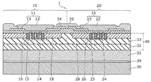
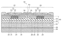
- FIG. 1A is a cross-sectional view of the semiconductor device according to the first embodiment.
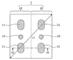
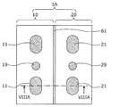
- 1B is a top view showing an example of the electrode configuration of the semiconductor device according to Embodiment 1.
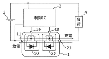
- FIG. FIG. 2A is a circuit diagram showing a first application example to the charge / discharge circuit of the semiconductor device according to the first embodiment.
- FIG. 2B is a circuit diagram in a case where an application example to the charge / discharge circuit is configured by only a unidirectional transistor.
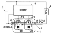
- FIG. 2C is a circuit diagram showing a second application example to the charge / discharge circuit of the semiconductor device according to the first embodiment.
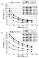
- FIG. 3A is a graph showing the on-resistance with respect to the thickness of the metal layer in the semiconductor device according to Comparative Example 1.
- FIG. 3B is a graph showing the on-resistance and the amount of warpage with respect to the thickness of the metal layer / the thickness of the semiconductor layer in the semiconductor device according to Comparative Example 2.
- FIG. 4A is a diagram illustrating a basic model for deriving warpage occurring in a multilayer body.
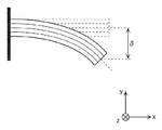
- FIG. 4B is a schematic side view for explaining the amount of warpage ⁇ occurring in the multilayer body.
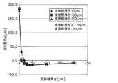
- FIG. 5 is a graph showing the amount of warpage with respect to the thickness of the adhesive layer and the thickness of the support.
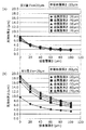
- FIG. 6A is a graph showing the relationship among the thicknesses of the metal layer, the adhesive layer, and the support for setting the warping amount to 20 ⁇ m when the thickness of the semiconductor layer is fixed, calculated using the effective value calculation formula. It is.
- FIG. 6B is a graph showing the relationship between the thicknesses of the semiconductor layer, the adhesive layer, and the support for setting the warping amount to 20 ⁇ m when the thickness of the metal layer is fixed, calculated using the effective value calculation formula. It is.
- FIG. 7 is a graph defining the relationship between the thickness of the support and the thickness of the adhesive layer for setting the warpage amount to the target value and the allowable value in the semiconductor device according to the first embodiment.
- FIG. 8A is a cross-sectional view of the semiconductor device according to Modification 1 of Embodiment 1.
- 8B is a top view showing an example of the electrode configuration of the semiconductor device according to Modification 1 of Embodiment 1.
- FIG. FIG. 9 is a cross-sectional view of the semiconductor device according to the second modification of the first embodiment.
- FIG. 10A is a cross-sectional view showing a first step of the method of manufacturing a semiconductor device according to the first embodiment.
- FIG. 10B is a cross-sectional view showing a second step of the method of manufacturing a semiconductor device according to the first embodiment.
- FIG. 10C is a cross-sectional view showing a third step of the method of manufacturing a semiconductor device according to the first embodiment.
- FIG. 11A is a cross-sectional view showing a fourth step of the method of manufacturing a semiconductor device according to the first embodiment.
- FIG. 11B is a cross-sectional view showing a fifth step of the method of manufacturing a semiconductor device according to the first embodiment.
- FIG. 12A is a cross-sectional view showing a sixth step of the method of manufacturing a semiconductor device according to the first embodiment.
- FIG. 12B is a cross-sectional view showing a seventh step of the method for manufacturing the semiconductor device according to the first embodiment.
- FIG. FIG. 13 is a cross-sectional view showing an eighth step of the method of manufacturing a semiconductor device according to the first embodiment.
- FIG. 14 is a cross-sectional view showing a ninth step of the method of manufacturing a semiconductor device according to the first embodiment.
- the on-current flowing through the metal layer flows in a direction parallel to the main surface of the metal layer. Therefore, it is preferable to increase the thickness of the metal layer from the viewpoint of reducing the on-resistance.
- the thermal expansion coefficient of the metal layer becomes dominant as the metal layer becomes thicker. Therefore, the thickness of the metal layer is 1 ⁇ 4 that of the semiconductor substrate. The following is preferred. In this case, the thickness of the metal layer for reducing the on-resistance is limited by the thickness of the semiconductor substrate. Depending on the thickness of the semiconductor substrate, the metal layer becomes thin and sufficient on-resistance cannot be obtained.
- an insulating film is formed on the opposite side of the metal layer from the semiconductor substrate for the purpose of preventing scratches and scratches.
- This insulating coating is composed of a coating-type organic material, an organic tape, or an inorganic oxide thin film from the viewpoint of preventing peeling from the metal layer and reducing the thickness of the semiconductor device. For this reason, the insulating coating has a function of suppressing the warpage of the semiconductor device caused by the metal layer, but when the metal layer is thickened for the purpose of reducing the on-resistance, the insulating coating is caused by the metal layer. It does not have sufficient stress to suppress warpage of the semiconductor device.
- the present inventor has a metal layer having a thickness of 20 ⁇ m or more that can provide a practical low on-resistance when a semiconductor device having two vertical MOS transistors is applied as a charge / discharge circuit.
- the semiconductor device the inventors have found a configuration of the semiconductor device in which the warpage amount of the semiconductor substrate and the metal layer is not more than a predetermined value.
- the semiconductor device 1 according to the present disclosure is a CSP (Chip Size Package) type multi-transistor chip in which two vertical MOS (Metal Oxide Semiconductor) transistors are formed on a semiconductor substrate.
- the two vertical MOS transistors are power transistors and are so-called trench MOS FETs (Field Effect Transistors).
- the semiconductor device 1 according to the present embodiment is not applied to a device classified as optoelectronics such as a solid-state imaging device.
- FIG. 1A is a cross-sectional view showing an example of the structure of the semiconductor device 1.
- FIG. 1B is a top view showing an example of the electrode configuration of the semiconductor device 1 according to the first embodiment.
- the cross-sectional view of FIG. 1A is a view of a cut surface taken along the line IA-IA of FIG. 1B.
- the semiconductor device 1 includes a semiconductor substrate 32, a low-concentration impurity layer 33, a metal layer 31, an adhesive layer 39, a support 30, and a first vertical MOS transistor 10 (hereinafter referred to as “first vertical MOS transistor 10”). Transistor 10) and a second vertical MOS transistor 20 (hereinafter referred to as transistor 20).
- the semiconductor device 1 when the semiconductor substrate 32 is viewed in plan, the semiconductor device 1 includes two first source electrodes 11, two second source electrodes 21, one first gate electrode 19, One second gate electrode 29 is provided.
- a first source electrode 11, a first gate electrode 19, and a first source electrode 11 are formed in this order on the upper surface of the transistor 10 along a direction perpendicular to the direction in which the transistors 10 and 20 face each other.
- a second source electrode 21, a second gate electrode 29, and a second source electrode 21 are provided on the upper surface of the transistor 20 along a direction perpendicular to the direction in which the transistors 10 and 20 face each other. It is formed in order.
- the semiconductor substrate 32 contains a first conductivity type impurity and is made of silicon.
- the semiconductor substrate 32 is, for example, an N-type silicon substrate.
- the low-concentration impurity layer 33 is formed in contact with the upper surface of the semiconductor substrate 32 (upper main surface in FIG. 1A), and contains a first conductivity type impurity having a concentration lower than the concentration of the first conductivity type impurity of the semiconductor substrate 32. Including.
- the low concentration impurity layer 33 may be formed on the semiconductor substrate 32 by, for example, epitaxial growth.
- a stacked body of a semiconductor substrate 32 and a low concentration impurity layer 33 is defined as a semiconductor layer 40.
- the metal layer 31 is formed in contact with the entire lower surface (lower main surface in FIG. 1A) of the semiconductor substrate 32, and is composed of only a metal material.
- the metal layer 31 may be made of a metal material including any one or more of silver, copper, gold, and aluminum.
- the support 30 is bonded to the entire lower surface of the two main surfaces of the metal layer 31 that is not in contact with the semiconductor substrate 32 via an adhesive layer 39, and is made of a ceramic material.
- the ceramic material constituting the support 30 is particularly exemplified by silicon, but quartz, sapphire, borosilicate glass, soda-lime glass, etc. are also exemplified.
- the adhesive layer 39 is disposed in contact with the metal layer 31 and the support 30 and is a layer for bonding the metal layer 31 and the support 30.
- the adhesive layer 39 is formed by curing, for example, an adhesive made of an acrylic resin or an epoxy resin, or DAF (Die Attach Film).
- the transistor 10 is formed in the first region (the left half region in FIG. 1A) in the low concentration impurity layer 33, and is in a different cross section from the first source electrode 11 formed on the upper surface of the low concentration impurity layer 33. It has the 1st gate electrode 19 (refer FIG. 1B).
- a first body region 18 containing an impurity of a second conductivity type different from the first conductivity type is formed.
- a first source region 14 including a first conductivity type impurity, a first gate conductor 15, and a first gate insulating film 16 are formed.
- the first source electrode 11 includes a first portion 12 and a second portion 13, and the first portion 12 is connected to the first source region 14 and the first body region 18 via the second portion 13. It is connected to the.
- the first gate electrode 19 is connected to the first gate conductor 15.
- the first portion 12 of the first source electrode 11 is a layer that exhibits good bonding properties with a conductive bonding material such as solder at the time of mounting.
- a conductive bonding material such as solder at the time of mounting.
- any one of nickel, titanium, tungsten, and palladium is not limited. Or a metal material including one or more of them.
- the surface of the first portion 12 may be plated with gold or the like.
- the second portion 13 of the first source electrode 11 is a layer that connects the first portion 12 and the semiconductor layer 40, and as one non-limiting example, any one of aluminum, copper, gold, and silver is used. You may be comprised with the metal material containing the above.
- the transistor 20 is formed in the second region adjacent to the upper surface of the semiconductor substrate 32 in the low concentration impurity layer 33 (the right half region in FIG. 1A) and formed on the upper surface of the low concentration impurity layer 33.
- the second source electrode 21 and the second gate electrode 29 in another cross section are provided.
- a second body region 28 containing an impurity of a second conductivity type different from the first conductivity type is formed.
- a second source region 24 containing a first conductivity type impurity, a second gate conductor 25, and a second gate insulating film 26 are formed.
- the second source electrode 21 includes a first portion 22 and a second portion 23, and the first portion 22 is connected to the second source region 24 and the second body region 28 via the second portion 23. It is connected to the.
- the second gate electrode 29 is connected to the second gate conductor 25.
- the first portion 22 of the second source electrode 21 is a layer that exhibits good bonding properties with a conductive bonding material such as solder at the time of mounting.
- a conductive bonding material such as solder at the time of mounting.
- any one of nickel, titanium, tungsten, and palladium is not limited. Or a metal material including one or more of them.
- the surface of the first portion 22 may be plated with gold or the like.
- the second portion 23 of the second source electrode 21 is a layer that connects the first portion 22 and the semiconductor layer 40.
- any one of aluminum, copper, gold, and silver is used. You may be comprised with the metal material containing the above.
- the first body region 18 and the second body region 28 are covered with an interlayer insulating layer 34 having an opening, and are connected to the first source region 14 and the second source region 24 through the opening of the interlayer insulating layer 34. Electrode second portions 13 and 23 are provided.
- the interlayer insulating layer 34 and the second portions 13 and 23 of the source electrode are covered with a passivation layer 35 having an opening, and the first portions of the source electrode connected to the second portions 13 and 23 through the opening of the passivation layer 35, respectively.
- Portions 12 and 22 are provided.
- the first source electrode 11, the first gate electrode 19, the second source electrode 21, and the second gate electrode 29 are made of a conductive bonding material such as solder. Via, the electrode provided on the mounting substrate is bonded face down. In this case, as the warp of the semiconductor device 1 is larger, the first source electrode 11, the first gate electrode 19, the second source electrode 21, the second gate electrode 29, and the electrodes provided on the mounting substrate The electrical connection of becomes unstable. That is, in order to further stabilize the mounting of the semiconductor device 1 on the mounting substrate, it is necessary to reduce the warpage of the semiconductor device 1.
- the semiconductor substrate 32 functions as a common drain region in which the first drain region of the transistor 10 and the second drain region of the transistor 20 are shared. Further, the semiconductor device 1 has a bidirectional path that flows between the first source electrode 11 and the second source electrode 21 via the first drain region, the metal layer 31, and the second drain region. The main current path.
- FIG. 2A is a circuit diagram showing a first application example of the charge / discharge circuit of the semiconductor device 1. As shown in FIG. 2A, the semiconductor device 1 controls the discharge from the battery 3 to the load 4 and the charge from the load 4 to the battery 3 in accordance with a control signal given from the control IC 2.
- FIG. 2B is a circuit diagram in a case where a similar application example is configured by only a unidirectional transistor 10.
- the discharge current can be stopped by turning off the transistor 10, but the charging current can be stopped between the first body region 18 and the low-concentration impurity layer 33 even when the transistor 10 is turned off. Since the body diode formed in this manner flows in the forward direction (the direction from the first body region 18 to the low-concentration impurity layer 33), it cannot be stopped. Therefore, a bidirectional transistor is required to enable complete current interruption in both the discharging and charging directions.
- FIG. 2C is a circuit diagram showing a second application example to the charge / discharge circuit of the semiconductor device 1.
- the semiconductor device 1 cuts off the discharge current by turning off the transistor 10 and turns off the charging current by turning off the transistor 20 in accordance with a control signal given from the control IC 2. Cut off.
- the first conductivity type is N type
- the second conductivity type is P type
- the first source region 14 the second source region 24, the semiconductor substrate 32, and the low conductivity type.
- the concentration impurity layer 33 may be an N-type semiconductor
- the first body region 18 and the second body region 28 may be P-type semiconductors.
- the first conductivity type is P type
- the second conductivity type is N type
- the first source region 14, the second source region 24, the semiconductor substrate 32, and the low concentration impurity layer 33 are P type semiconductors
- the first body region 18 and the second body region 28 may be N-type semiconductors.
- the semiconductor device 1 shown in FIG. 1A will be described as a so-called N-channel transistor in which the first conductivity type is N-type and the second conductivity type is P-type.
- a high voltage is applied to the first source electrode 11, a low voltage is applied to the second source electrode 21, and the first gate electrode 19 (first When a voltage higher than the threshold is applied to the gate conductor 15) and the second gate electrode 29 (second gate conductor 25), a channel is formed in the vicinity of the first gate insulating film 16 and the second gate insulating film 26.
- the formed current flows through the path of the first source electrode 11 -the first body region 18 -the first drain region -the metal layer 31 -the second drain region -the second body region 28 -the second source electrode 21. Flows.
- FIG. 2A is the on state of the semiconductor device 1 in which the transistors 10 and 20 are turned on and the on current flows.
- the on-current between the transistors 10 and 20 flows through the metal layer 31. Therefore, by increasing the thickness of the metal layer 31, the cross-sectional area of the on-current path is enlarged, and the on-resistance of the semiconductor device 1 is reduced.
- the PN junctions between the first body region 18 and the low concentration impurity layer 33 and between the second body region 28 and the low concentration impurity layer 33 constitute a body diode.
- a body diode formed between the first body region 18 and the low-concentration impurity layer 33 is referred to as a first body diode, and is formed between the second body region 28 and the low-concentration impurity layer 33.
- the body diode is referred to as a second body diode.
- the voltage application conditions to the first source electrode 11 and the second source electrode 21 are opposite. If the voltage of the first gate electrode 19 (first gate conductor 15) is lower than the threshold with reference to one source electrode 11, a channel is not formed in the vicinity of the gate insulating film 16 of the transistor 10, and the semiconductor The device 1 enters an off state where no on-current flows.
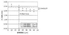
- FIG. 3A is a graph showing the on-resistance with respect to the thickness of the metal layer in the semiconductor device according to Comparative Example 1.
- the semiconductor device according to Comparative Example 1 has a configuration in which the adhesive layer 39 and the support 30 are not formed with respect to the semiconductor device 1 illustrated in FIGS. 1A and 1B.
- the semiconductor device according to Comparative Example 1 it is assumed that (1) the semiconductor layer 40 has a thickness of 43 ⁇ m and (2) the semiconductor layer 40 has a thickness of 78 ⁇ m.
- the on-resistance of the semiconductor device when the thickness of the metal layer 31 was changed in the range of 10 to 40 ⁇ m was measured. For each sample, the on-resistance was measured by either the first method of measuring the sample mounted on the evaluation substrate or the second method of applying the probe to the bare chip sample. Differences in measured values caused by differences in measurement methods were corrected as appropriate.
- Table 1 shows parameters of the semiconductor device according to Comparative Example 1.
- the on-resistance decreases as the metal layer 31 is thickened.
- the on-resistance is 2.2 to 2.4 m ⁇ or less as a 20 V withstand voltage specification due to restrictions on shortening the charging time and realizing rapid charging. Desired.
- the thickness of the metal layer 31 that satisfies the on-resistance of 2.4 m ⁇ or less needs to be 20 ⁇ m or more.
- FIG. 3B shows the ratio of the thickness of the metal layer 31 to the thickness of the semiconductor layer 40 in the semiconductor device according to Comparative Example 2 (hereinafter, sometimes referred to as metal layer 31 thickness / semiconductor layer 40 thickness). It is a graph which shows the relationship between on-resistance and curvature amount.
- the semiconductor device according to Comparative Example 2 has a configuration in which the adhesive layer 39 and the support 30 are not formed with respect to the semiconductor device 1 illustrated in FIGS. 1A and 1B.
- the on-resistance and the semiconductor substrate when the thickness of the metal layer 31 is changed in the range of 10 ⁇ m to 40 ⁇ m and the thickness of the semiconductor layer 40 is changed in the range of 28 to 93 ⁇ m The amount of warpage of the laminate of 32 and the metal layer 31 was measured. For the amount of warpage, place the bare chip sample under a heat load cycle with a maximum temperature of 250 ° C that simulates the reflow process, measure the shape of the bare chip by the moire method, and record the maximum value of the measured warpage amount. did.
- Table 2 shows parameters of the semiconductor device according to Comparative Example 2.
- the ON resistance decreases as the thickness of the metal layer 31 / the thickness of the semiconductor layer 40 increases.
- the amount of warpage increases as the thickness of the metal layer 31 / the thickness of the semiconductor layer 40 increases.
- the thickness of the metal layer 31 / the thickness of the semiconductor layer 40 satisfying an on-resistance of 2.4 m ⁇ or less is larger than 0.27.
- the amount of warpage is 20 ⁇ m or more.
- the amount of warpage increases, stable mounting becomes difficult and problems occur during face-down mounting on a mounting board. For example, (1) solder bonding between the electrode on the semiconductor device and the electrode on the mounting substrate is incomplete, (2) voids are generated in the solder, and (3) the solder protrudes from the electrode. Problems such as short-circuit between electrodes occur.
- the thickness of the metal layer 31 is 20 ⁇ m or more and ( 2) It is necessary that the thickness of the metal layer 31 / the thickness of the semiconductor layer 40 is larger than 0.27.
- the warpage amount is 20 ⁇ m or more.
- the adhesive layer 39 is formed in contact with the entire main surface of the metal layer 31 opposite to the semiconductor substrate 32, A support 30 made of a ceramic material is formed in contact with the entire main surface of the adhesive layer 39 opposite to the metal layer 31.
- the physical constants such as the thermal expansion coefficient and the Young's modulus, which are the main factors of stress generation of the support 30 made of the ceramic material, are closer to the physical constant of the semiconductor substrate 32 than the physical constant of the metal layer 31 made of the metal material. Has a value. That is, thermal expansion stress in a direction that cancels the thermal expansion stress generated by the bonding between the semiconductor substrate 32 and the metal layer 31 is generated by the bonding between the support 30 and the metal layer 31. Thereby, in the main surface which the metal layer 31 opposes, since the thermal expansion stress is balanced, the curvature of the laminated body of the metal layer 31 and the semiconductor layer 40 can be suppressed.
- a conductive layer is formed in contact with the main surface of the metal layer opposite to the semiconductor substrate.
- the physical constant of the conductive layer has a value closer to the physical constant of the metal layer than the physical constant of the semiconductor substrate. For this reason, in the semiconductor device according to Patent Document 1, no stress in a direction to cancel the stress generated by the bonding between the semiconductor substrate and the metal layer is generated by the bonding between the conductive layer and the metal layer.
- a thin film material such as an insulating coating (a coating type organic material, an organic tape, or an inorganic oxide thin film) disclosed in Patent Document 2 is insufficient.
- the semiconductor device 1 is configured such that the adhesive layer 39 is interposed between the metal layer 31 and the support 30.
- the metal layer 31 is opposite to the semiconductor substrate 32 in order to suppress the thermal expansion stress applied to the metal layer 31 having a thickness of 20 ⁇ m or more and a ratio of the thickness to the semiconductor layer 40 being larger than 0.27.
- the chip size package type semiconductor device 1 that achieves both reduction of on-resistance and suppression of warpage of the semiconductor device 1 by forming the adhesive layer 39 and the support 30 made of a ceramic material. It becomes.
- the ceramic material of the support 30 is, for example, silicon. Therefore, even when compared with silicon nitride and silicon oxide, the machinability when the semiconductor device is separated into pieces by dicing is improved. Further, it is easier to obtain materials than silicon nitride and silicon oxide, and the cost is low.
- the metal material of the metal layer 31 is, for example, silver (Ag). This makes it possible to effectively reduce the on-resistance as compared with copper (Cu) or the like that is generally used as a metal material.
- the metal layer 31 may be thicker than the semiconductor layer 40. This can contribute to further reduction of on-resistance.
- the support 30 may be thinner than the semiconductor layer 40.
- the adhesive layer 39 between the metal layer 31 and the support 30 is interposed, the semiconductor substrate 32 is provided even when the support 30 is thinner than the semiconductor layer 40. In addition, it is possible to contribute to the reduction of the warpage amount of the metal layer 31.
- the adhesive layer 39 may be a conductive adhesive, for example, conductive DAF.
- conductive DAF conductive DAF
- the material for the conductive adhesive include silver paste. This can contribute to further reduction of on-resistance.
- the theoretical formula of the amount of warpage generated when a plurality of multilayers having different physical constants are bonded together is expressed as 4 of the semiconductor layer 40, the metal layer 31, the adhesive layer 39, and the support 30. This is applied to the semiconductor device 1 according to the present embodiment, which is composed of layers (step S10).
- the theoretical formula is set so that the warpage amount ⁇ of the semiconductor device 1 according to the present embodiment derived based on the theoretical formula matches the calculated value in the warpage calculation simulator constructed using the finite element method. Fitting is performed (step S20).
- the adhesion when the warpage amount ⁇ e of the semiconductor device 1 according to the present embodiment is 20 ⁇ m or less and 40 ⁇ m or less.
- the thicknesses of the layer 39 and the support 30 are derived (step S30).
- step S10 will be described.
- FIG. 4A is a diagram illustrating a basic model for deriving the amount of warpage occurring in the multilayer body.
- a first layer having (thermal expansion coefficient ⁇ 1 , Young's modulus E 1 ) and thickness t 1
- a third layer having two layers, (thermal expansion coefficient ⁇ 3 , Young's modulus E 3 ) and thickness t 3
- a fourth layer having (thermal expansion coefficient ⁇ 4 , Young's modulus E 4 ) and thickness t 4 Are joined in this order toward the negative y-axis direction. It is assumed that the length L and width (depth) b of each layer viewed from the y-axis direction are the same for all four layers.
- FIG. 4B is a schematic side view for explaining the amount of warpage ⁇ occurring in the multilayer body. As shown in the figure, the amount by which the end of the multilayer body in the positive x-axis direction shifts from the horizontal position in the negative y-axis direction due to the stress generated in the multilayer body is defined as a warpage amount ⁇ .
- Table 3 shows an example of the warpage amount ⁇ obtained using the above formulas 1 and 2.
- Table 4 shows other parameters used when the warpage amount ⁇ of Table 3 was obtained.
- the width b is set to 1 mm. This is because the width b appears in both the denominator and the numerator and is offset in calculating the warpage amount ⁇ . It is.
- step S20 the above equations 1 and 2 are fitted so that the warpage amount ⁇ derived based on the above equations 1 and 2 matches the calculated value ⁇ s in the warpage calculation simulator.
- the warpage calculation simulator used for the fitting is a customized structure analysis software (manufactured by ANSYS) using finite element method analysis using a necessary amount of warpage measurement data.
- step S30 will be described.
- the warpage amount of the semiconductor device 1 according to the present embodiment is (1) 20 ⁇ m or less, and (2 ) The thicknesses of the adhesive layer 39 and the support 30 when the thickness is 40 ⁇ m or less are derived.
- FIG. 5 is a graph showing a change in the warpage amount ⁇ e with respect to the thickness of the adhesive layer 39 and the thickness of the support 30 calculated using the effective value calculation formula.
- the relationship between the thickness of 30 and the warpage amount ⁇ e is shown.
- the other parameters have the values shown in Table 4.
- the warpage amount ⁇ e takes a negative value
- the minimum point of the warpage amount ⁇ e in the reverse warp is about 10 ⁇ m and does not exceed 20 ⁇ m. Therefore, when the conditions for the thickness of the adhesive layer 39 and the support 30 are determined, the condition for making the forward warpage 20 ⁇ m or less may be set.
- the semiconductor device 1 In determining the thickness of the adhesive layer 39 and the support 30 as described above, the semiconductor device 1 according to the present embodiment has four layers having different physical constants and different thicknesses. Many. Therefore, the thickness of the adhesive layer 39 and the support 30 is calculated according to the following policy.
- the main parameters are the thicknesses of the four layers and the warpage amount ⁇ e.
- the standard value of the warpage amount ⁇ e is set to a first standard value of 20 ⁇ m and a second standard value of 40 ⁇ m.
- the feature of the semiconductor device 1 according to the present embodiment is that the adhesive layer 39 and the support 30 are arranged in order to suppress the warp that occurs in the semiconductor layer 40 and the metal layer 31, and thus the warp amount.
- the thickness of the support 30 that satisfies the standard value of ⁇ e is defined in a format that depends on the thickness of the adhesive layer 39. That is, a function that can determine the thickness of the support 30 is derived according to the thickness of the adhesive layer 39 to be used.
- FIG. 6A shows a case where the thickness of the semiconductor layer 40 calculated using the effective value calculation formula is fixed ((a) is the thickness of the semiconductor layer 40 10 ⁇ m, (b) is the thickness of the semiconductor layer 40 80 ⁇ m). 4 is a graph showing the relationship among the thicknesses of the metal layer 31, the adhesive layer 39, and the support 30 for setting the warpage amount ⁇ e to 20 ⁇ m.
- FIG. 6B shows the case where the thickness of the metal layer 31 calculated using the effective value calculation formula is fixed ((a) is the thickness of the metal layer 31 and (b) is the thickness of the metal layer 31 is 70 ⁇ m. Is a graph showing the relationship among the thicknesses of the semiconductor layer 40, the adhesive layer 39, and the support 30 for setting the warpage amount ⁇ e to 20 ⁇ m.
- the graphs as shown in (a) and (b) of FIG. 6A are obtained even when the thickness of the semiconductor layer 40 is 20 ⁇ m, 40 ⁇ m, and 60 ⁇ m, and also as shown in (a) and (b) of FIG. 6B. Is obtained using the effective value calculation formula even when the thickness of the metal layer 31 is 40 ⁇ m, 50 ⁇ m, and 60 ⁇ m. From the graph obtained in this way, the thickness of the support 30 is extracted for each thickness of the adhesive layer 39 that sets the warpage amount ⁇ e to 20 ⁇ m. At this time, the thickness of the support 30 for each thickness of the adhesive layer 39 that changes the thickness of the semiconductor layer 40 and the thickness of the metal layer 31 to change the warpage amount ⁇ e to 20 ⁇ m changes.
- the maximum value of the thickness of the support 30 for each thickness of the adhesive layer 39 is extracted.
- the same extraction process is also applied to the thickness of the support 30 for each thickness of the adhesive layer 39 in which the warpage amount ⁇ e is 40 ⁇ m.
- Table 5 shows combinations of thicknesses of the support 30 for each thickness of the adhesive layer 39 obtained by this extraction process.
- Table 6 shows other parameters used when the warpage amount ⁇ e in Table 5 was obtained.
- FIG. 7 is a graph that defines the relationship of the thickness of the support 30 with respect to the thickness of the adhesive layer 39 for making the warpage amounts 20 ⁇ m and 40 ⁇ m in the semiconductor device 1 according to the first embodiment.
- the extracted data shown in Table 5 are plotted. From the graph shown in the figure, (1) an approximate expression representing the relationship of the thickness of the support 30 to the thickness of the adhesive layer 39 for setting the warpage amount ⁇ e to 20 ⁇ m (target value), and (2) the warpage amount ⁇ e.
- Approximate expression expressing the relationship of the thickness of the support 30 to the thickness of the adhesive layer 39 to 20 ⁇ m (allowable value), (3) Support to the thickness of the adhesive layer 39 to set the warping amount ⁇ e to 40 ⁇ m (target value)
- An approximate expression representing the relationship between the thicknesses of 30
- (4) an approximate expression representing the relationship between the thickness of the support 30 and the thickness of the adhesive layer 39 for setting the warpage amount ⁇ e to 40 ⁇ m (allowable value). From these approximate expressions, the relationship of the thickness of the support 30 to the thickness of the adhesive layer 39 that suppresses the warpage amount of the semiconductor device 1 is expressed by Expressions 4 to 7.
- the thickness of the adhesive layer 39 is t 3 ( ⁇ m) and the thickness of the support 30 is t 4 ( ⁇ m)
- the thickness of 30 is expressed by Equation 4 below.
- the length L of each layer is 3.4 mm or less.
- the thermal expansion coefficient ⁇ 3 of the adhesive layer 39 is 1.1 (ppm / ° C.) or less and the Young's modulus E 3 of the adhesive layer 39 is 50 (GPa) or less, the warpage amount of the semiconductor device 1 is 20 ⁇ m. It is possible to:
- the length L of each layer is 4.0 mm or less.
- the thermal expansion coefficient ⁇ 3 of the adhesive layer 39 is 5.0 (ppm / ° C.) or less and the Young's modulus E 3 of the adhesive layer 39 is 100 (GPa) or less, the warpage amount of the semiconductor device 1 is 20 ⁇ m. It is possible to:
- the length L of each layer is 3.4 mm or less
- the thermal expansion coefficient ⁇ 3 of the adhesive layer 39 is 1.1 (ppm / ° C.) or less and the Young's modulus E 3 of the adhesive layer 39 is 50 (GPa) or less
- the warpage amount of the semiconductor device 1 is 40 ⁇ m. It is possible to:
- the length L of each layer is 4.0 mm or less.
- the thermal expansion coefficient ⁇ 3 of the adhesive layer 39 is 5.0 (ppm / ° C.) or less and the Young's modulus E 3 of the adhesive layer 39 is 100 (GPa) or less, the warpage amount of the semiconductor device 1 is 40 ⁇ m. It is possible to:
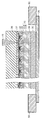
- FIG. 8A is a cross-sectional view of a semiconductor device 1A according to Modification 1 of Embodiment 1.
- FIG. 8B is a top view showing an example of the electrode configuration of the semiconductor device 1A according to the first modification of the first embodiment.
- the cross-sectional view of FIG. 8A is a view of a cut surface taken along the line VIIIA-VIIIA of FIG. 8B.
- the semiconductor device 1 ⁇ / b> A includes a semiconductor substrate 32, a low concentration impurity layer 33, a metal layer 31, an adhesive layer 39, a support 30, a transistor 10, and a transistor 20. As shown in FIG.
- the semiconductor device 1A when the semiconductor substrate 1A is viewed in plan, the semiconductor device 1A includes two first source electrodes 11, two second source electrodes 21, one first gate electrode 19, and One second gate electrode 29 is provided.
- a first source electrode 11, a first gate electrode 19, and a first source electrode 11 are formed in this order on the upper surface of the transistor 10 along a direction perpendicular to the direction in which the transistors 10 and 20 face each other.
- a second source electrode 21, a first gate electrode 29, and a first source electrode 21 are provided on the upper surface of the transistor 20 along a direction perpendicular to the direction in which the transistors 10 and 20 face each other. It is formed in order. Note that the number and arrangement of source electrodes and gate electrodes included in one transistor are not limited to those illustrated in FIG. 8B.
- the semiconductor device 1A according to the present modification differs from the semiconductor device 1 according to the first embodiment only in that the notch 61 is formed at the boundary between the transistors 10 and 20.
- the description of the same configuration as that of the semiconductor device 1 according to the first embodiment will be omitted, and a description will be given focusing on different configurations.
- the boundary between the first region of the transistor 10 and the second region of the transistor 20 is from the upper surface side of the semiconductor device 1A.
- a cut portion 61 is formed toward the lower surface side. Further, the cut portion 61 is formed up to the low concentration impurity layer 33. Note that the lowermost end of the cut portion 61 of the semiconductor device 1 ⁇ / b> A according to this modification is located on the upper surface side of the semiconductor device 1 ⁇ / b> A with respect to the lower surface of the semiconductor substrate 32.
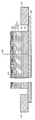
- FIG. 9 is a cross-sectional view of the semiconductor device 1B according to the second modification of the first embodiment. Note that a top view showing an example of the electrode configuration of the semiconductor device 1B according to the second modification of the first embodiment is omitted because it is the same as the top view of the semiconductor device 1A shown in FIG. 8B.
- the semiconductor device 1 ⁇ / b> B includes a semiconductor substrate 32, a low concentration impurity layer 33, a metal layer 31, an adhesive layer 39, a support 30, a transistor 10, and a transistor 20.
- the semiconductor substrate 32 is viewed in plan, the semiconductor device 1B includes two first source electrodes 11, two second source electrodes 21, one first gate electrode 19, and one second gate electrode. 29.
- a first source electrode 11, a first gate electrode 19, and a first source electrode 11 are formed in this order on the upper surface of the transistor 10 along a direction perpendicular to the direction in which the transistors 10 and 20 face each other. Has been.
- a second source electrode 21, a first gate electrode 29, and a first source electrode 21 are provided on the upper surface of the transistor 20 along a direction perpendicular to the direction in which the transistors 10 and 20 face each other. It is formed in order. Note that the number and arrangement of source electrodes and gate electrodes included in one transistor are not limited to those illustrated in FIG. 8B.
- the semiconductor device 1B according to the present modification differs from the semiconductor device 1 according to the first embodiment only in that the notch 62 is formed at the boundary between the transistors 10 and 20.
- the description of the same configuration as that of the semiconductor device 1 according to the first embodiment will be omitted, and a description will be given focusing on different configurations.
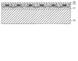
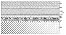
- FIG. 10A is a cross-sectional view showing a first step of the method of manufacturing semiconductor device 1 according to the first embodiment.
- FIG. 10B is a cross-sectional view showing a second step of the method of manufacturing semiconductor device 1 according to the first embodiment.
- FIG. 10C is a cross-sectional view showing a third step of the method of manufacturing a semiconductor device according to the first embodiment.
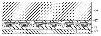
- a low-concentration impurity layer 33 is formed on one main surface of a semiconductor substrate 32A, and an element region is formed in the surface region of the low-concentration impurity layer 33.
- electrodes first source electrode, second source electrode mainly made of a metal such as Al or Cu are formed at predetermined positions on the element region.
- a temporary adhesive 37 is applied to one main surface side of the semiconductor substrate 32A. At this time, it is desirable to make the temporary adhesive 37 thicker than the unevenness of the electrode and the element region. Further, the glass substrate 36 is placed on the temporary adhesive 37 and pressed to adhere. At this time, in order to prevent bubbles from entering between the glass substrate 36 and the temporary adhesive 37, it is desirable to bond in a vacuum chamber.
- the thickness of the semiconductor substrate 32 ⁇ / b> A is set to a desired thickness (on the back side opposite to one main surface of the semiconductor substrate 32 ⁇ / b> A so that the required electrical characteristics (on-resistance) can be realized.
- the semiconductor substrate 32 having a desired thickness is formed by back grinding to preferably 50 ⁇ m or less. Further, it is desirable to perform a mirror surface treatment such as CMP.
- FIG. 11A is a cross-sectional view showing a fourth step of the method of manufacturing semiconductor device 1 according to the first embodiment.
- FIG. 11B is a cross-sectional view showing a fifth step of the method of manufacturing semiconductor device 1 according to the first embodiment.
- a metal layer 31 is formed on the back surface opposite to the one main surface of the semiconductor substrate 32.
- the first metal layer 31 ⁇ / b> A is formed on the entire back surface of the semiconductor substrate 32 by vapor deposition so as to make ohmic contact with the semiconductor substrate 32.
- the first metal layer 31 ⁇ / b> A for example, Ti and Ni are sequentially stacked from the side close to the back surface of the semiconductor substrate 32.
- the second metal layer 31B is formed on the first metal layer 31A. Specifically, it is formed using an electrolytic plating method. Here, it is preferable to use mainly Ag, Au, Cu or the like as the second metal layer 31B. In the following description, the first metal layer 31A and the second metal layer 31B are collectively referred to as the metal layer 31.
- an adhesive is applied on the metal layer 31 to form an adhesive layer 39.
- thermosetting resin such as an epoxy resin or a phenol resin
- the support 30 is made of an epoxy acrylate or acrylic acid as an adhesive when using a material transparent to ultraviolet rays, such as quartz, sapphire, borosilicate glass, and soda lime glass.
- An ultraviolet curable resin such as acrylate or urethane acrylate can also be used.
- the process for curing the adhesive will be described.
- the bonded wafers are heated in a thermostat at about 150 ° C. for 1 to 2 hours, for example.
- the adhesive is cured by heating, and the support 30 and the metal layer 31 are strongly bonded.
- the surface of the wafer 30 that has been bonded using an ultraviolet generator such as a high-pressure mercury lamp is irradiated with ultraviolet rays.
- the amount of light to be irradiated is, for example, 300 to 2000 mJ / cm 2 .
- FIG. 12A is a cross-sectional view showing a sixth step of the method of manufacturing semiconductor device 1 according to the first embodiment.
- FIG. 12B is a cross-sectional view showing a seventh step of the method of manufacturing semiconductor device 1 according to the first embodiment.
- the dicing tape 38 is attached to the surface of the support 30 and the ring frame 50, and the ring frame 50 is mounted.
- the temporary adhesive 37 and the glass substrate 36 are removed. Specifically, as shown in FIG. 12A, the portion of the temporary adhesive 37 in contact with the glass substrate 36 is modified by irradiating a laser beam 70 near the boundary surface between the temporary adhesive 37 and the glass substrate 36. The glass substrate 36 is removed from the wafer made of the semiconductor substrate 32. Thereafter, as shown in FIG. 12B, the temporary adhesive 37 is peeled and removed.
- FIG. 13 is a cross-sectional view showing an eighth step of the method of manufacturing semiconductor device 1 according to the first embodiment.
- the semiconductor substrate 32, the low-concentration impurity layer 33, the metal layer 31, the adhesive layer 39, and the support 30 are diced by using a dicing blade 80 such as a dicing saw, for example.
- a dicing blade 80 such as a dicing saw
- the metal layer 31 is sandwiched between the semiconductor substrate 32 and the support 30 in the manufacturing process of the semiconductor device 1 according to the present embodiment, the ductility like the metal layer 31 is formed on the outermost surface. Since there is no material, there is an effect that burrs are hardly generated on the cutting end face.
- FIG. 14 is a cross-sectional view showing a ninth step of the method of manufacturing a semiconductor device according to the first embodiment.
- notches 64 are made using a dicing blade 81 between a plurality of transistors.
- the process of FIG. 14 may be performed after the manufacturing process shown in FIGS. 10A to 10C, FIGS. 11A to 11B, and FIGS. 12A to 12B.
- individual processes are performed by the dicing process shown in FIG.
- the semiconductor device 1 is separated.
- a notch 64 is formed by a dicing blade 81 between a plurality of transistors formed in the semiconductor device 1.
- the semiconductor device has been described based on the embodiment, but the present disclosure is not limited to the embodiment. Unless it deviates from the gist of the present disclosure, various modifications conceived by those skilled in the art have been made in the present embodiment, and forms constructed by combining components in different embodiments are also applicable to one or more of the present disclosure. It may be included within the scope of the embodiments.
- the semiconductor device according to the present invention can be widely used as a CSP type semiconductor device in various semiconductor devices such as a bidirectional transistor, a unidirectional transistor, and a diode.
Landscapes
- Electrodes Of Semiconductors (AREA)
- Chemical & Material Sciences (AREA)
- Engineering & Computer Science (AREA)
- Ceramic Engineering (AREA)
- Dicing (AREA)
Abstract
Un dispositif à semi-conducteur est pourvu : d'un substrat semi-conducteur de type N (32) en silicium ; d'une couche d'impuretés à faible concentration de type N (33) en contact avec une surface supérieure du substrat semi-conducteur (32) ; d'une couche métallique (31) qui est en contact avec une surface inférieure entière du substrat semi-conducteur (32) et a une épaisseur qui n'est pas inférieure à 20 µm ; et des transistors (10 and 20) formés dans la couche d'impuretés à faible concentration. Le substrat semi-conducteur (32) fonctionne comme une zone de drain pour les transistors (10 et 20). Un trajet bidirectionnel d'écoulement entre les électrodes de source des transistors (10 et 20) via le substrat semi-conducteur (32) sur le côté du transistor (10), la couche métallique (31), et le substrat semi-conducteur (32) sur le côté du transistor (20) constitue un trajet de courant électrique principal. Un rapport d'épaisseur de la couche métallique (31) à une couche de semi-conducteur comprenant le substrat semi-conducteur (32) et la couche d'impuretés à faible concentration (33) est supérieur à 0,27. Le dispositif semi-conducteur (1) comprend en outre un corps de support (30) en matériau céramique qui adhère à la totalité de la surface inférieure de la couche métallique (31) uniquement via une couche adhésive (39).
Priority Applications (5)
| Application Number | Priority Date | Filing Date | Title |
|---|---|---|---|
| JP2018559114A JP7042217B2 (ja) | 2016-12-27 | 2017-12-21 | 半導体装置 |
| CN201780080128.5A CN110114888B (zh) | 2016-12-27 | 2017-12-21 | 半导体装置 |
| CN202210609454.3A CN114975302A (zh) | 2016-12-27 | 2017-12-21 | 半导体装置 |
| US16/447,100 US10854744B2 (en) | 2016-12-27 | 2019-06-20 | Semiconductor device |
| US17/070,211 US11056589B2 (en) | 2016-12-27 | 2020-10-14 | Semiconductor device |
Applications Claiming Priority (2)
| Application Number | Priority Date | Filing Date | Title |
|---|---|---|---|
| US201662439343P | 2016-12-27 | 2016-12-27 | |
| US62/439343 | 2016-12-27 |
Related Child Applications (1)
| Application Number | Title | Priority Date | Filing Date |
|---|---|---|---|
| US16/447,100 Continuation US10854744B2 (en) | 2016-12-27 | 2019-06-20 | Semiconductor device |
Publications (1)
| Publication Number | Publication Date |
|---|---|
| WO2018123799A1 true WO2018123799A1 (fr) | 2018-07-05 |
Family
ID=62710538
Family Applications (1)
| Application Number | Title | Priority Date | Filing Date |
|---|---|---|---|
| PCT/JP2017/045908 Ceased WO2018123799A1 (fr) | 2016-12-27 | 2017-12-21 | Dispositif semi-conducteur |
Country Status (5)
| Country | Link |
|---|---|
| US (2) | US10854744B2 (fr) |
| JP (1) | JP7042217B2 (fr) |
| CN (2) | CN110114888B (fr) |
| TW (1) | TW201830618A (fr) |
| WO (1) | WO2018123799A1 (fr) |
Cited By (13)
| Publication number | Priority date | Publication date | Assignee | Title |
|---|---|---|---|---|
| JP2020043164A (ja) * | 2018-09-07 | 2020-03-19 | 株式会社東芝 | 半導体装置 |
| WO2020129786A1 (fr) * | 2018-12-19 | 2020-06-25 | パナソニックセミコンダクターソリューションズ株式会社 | Dispositif à semi-conducteur |
| US10903359B2 (en) | 2018-06-19 | 2021-01-26 | Panasonic Semiconductor Solutions Co., Ltd. | Semiconductor device |
| US10930748B2 (en) | 2018-06-19 | 2021-02-23 | Panasonic Semiconductor Solutions Co., Ltd. | Semiconductor device |
| JP2021044287A (ja) * | 2019-09-06 | 2021-03-18 | 株式会社東芝 | 半導体装置およびその製造方法 |
| JPWO2022085765A1 (fr) * | 2020-10-23 | 2022-04-28 | ||
| JP7114824B1 (ja) * | 2021-09-17 | 2022-08-08 | ヌヴォトンテクノロジージャパン株式会社 | 半導体装置 |
| WO2022224889A1 (fr) * | 2021-04-22 | 2022-10-27 | 有限会社Mtec | Procédé de fabrication d'élément semi-conducteur et élément mosfet vertical |
| JP7323735B1 (ja) * | 2022-03-22 | 2023-08-08 | ヌヴォトンテクノロジージャパン株式会社 | 製造方法および半導体装置 |
| WO2023162735A1 (fr) * | 2022-02-24 | 2023-08-31 | ヌヴォトンテクノロジージャパン株式会社 | Dispositif à semi-conducteur |
| WO2023181460A1 (fr) * | 2022-03-22 | 2023-09-28 | ヌヴォトンテクノロジージャパン株式会社 | Procédé de production et dispositif à semi-conducteur |
| WO2024157764A1 (fr) * | 2023-01-23 | 2024-08-02 | ヌヴォトンテクノロジージャパン株式会社 | Dispositif à semi-conducteur |
| JP7651085B1 (ja) * | 2024-03-21 | 2025-03-25 | ヌヴォトンテクノロジージャパン株式会社 | 半導体装置 |
Families Citing this family (9)
| Publication number | Priority date | Publication date | Assignee | Title |
|---|---|---|---|---|
| WO2018123799A1 (fr) * | 2016-12-27 | 2018-07-05 | パナソニックIpマネジメント株式会社 | Dispositif semi-conducteur |
| US11367619B2 (en) | 2017-08-17 | 2022-06-21 | Semiconductor Components Industries, Llc | Semiconductor package electrical contacts and related methods |
| WO2019244387A1 (fr) * | 2018-06-19 | 2019-12-26 | パナソニックIpマネジメント株式会社 | Dispositif semi-conducteur |
| CN114823664B (zh) * | 2018-06-19 | 2025-06-20 | 新唐科技日本株式会社 | 半导体装置 |
| JP6909949B1 (ja) | 2019-10-21 | 2021-07-28 | ヌヴォトンテクノロジージャパン株式会社 | 半導体装置 |
| JP7470070B2 (ja) * | 2021-02-18 | 2024-04-17 | 株式会社東芝 | 半導体装置 |
| TWI844493B (zh) * | 2021-03-29 | 2024-06-01 | 日商新唐科技日本股份有限公司 | 半導體裝置 |
| JP7551554B2 (ja) * | 2021-03-30 | 2024-09-17 | 株式会社東芝 | 半導体装置 |
| US12563777B2 (en) * | 2023-05-19 | 2026-02-24 | Taiwan Semiconductor Manufacturing Co., Ltd. | Complementary field effect transistor with oblique conductive through substrate layer |
Citations (6)
| Publication number | Priority date | Publication date | Assignee | Title |
|---|---|---|---|---|
| JP2001127290A (ja) * | 1999-10-29 | 2001-05-11 | Nec Corp | 縦型電界効果トランジスタ及びその作製方法 |
| JP2004342718A (ja) * | 2003-05-14 | 2004-12-02 | Toshiba Corp | 半導体装置及びコンバータ |
| JP2007005657A (ja) * | 2005-06-24 | 2007-01-11 | Nec Electronics Corp | 半導体装置及び半導体装置の製造方法 |
| JP2008060105A (ja) * | 2006-08-29 | 2008-03-13 | Shindengen Electric Mfg Co Ltd | 半導体装置および該半導体装置の製造方法 |
| JP2015231033A (ja) * | 2014-06-06 | 2015-12-21 | ルネサスエレクトロニクス株式会社 | 半導体装置及び半導体装置の製造方法 |
| JP2016197737A (ja) * | 2016-06-29 | 2016-11-24 | 株式会社タムラ製作所 | 半導体素子及びその製造方法、並びに結晶積層構造体 |
Family Cites Families (23)
| Publication number | Priority date | Publication date | Assignee | Title |
|---|---|---|---|---|
| US6448624B1 (en) * | 1996-08-09 | 2002-09-10 | Denso Corporation | Semiconductor acceleration sensor |
| JP4164874B2 (ja) * | 2004-05-31 | 2008-10-15 | サンケン電気株式会社 | 半導体装置 |
| JP5124934B2 (ja) | 2005-02-04 | 2013-01-23 | ソニー株式会社 | 固体撮像素子及びその製造方法、撮像装置 |
| JP2010092895A (ja) | 2008-10-03 | 2010-04-22 | Sanyo Electric Co Ltd | 半導体装置及びその製造方法 |
| TW201015718A (en) | 2008-10-03 | 2010-04-16 | Sanyo Electric Co | Semiconductor device and method for manufacturing the same |
| US9257328B2 (en) * | 2008-11-26 | 2016-02-09 | Corning Incorporated | Glass-ceramic-based semiconductor-on-insulator structures and method for making the same |
| US8188484B2 (en) * | 2008-12-25 | 2012-05-29 | Rohm Co., Ltd. | Semiconductor device |
| JP4894910B2 (ja) * | 2009-01-15 | 2012-03-14 | 株式会社デンソー | 半導体装置の製造方法及び半導体装置並びにその半導体装置を内蔵する多層基板 |
| JP2010205761A (ja) | 2009-02-27 | 2010-09-16 | Sanyo Electric Co Ltd | 半導体装置およびその製造方法 |
| WO2011087994A2 (fr) * | 2010-01-12 | 2011-07-21 | Maxpower Semiconductor Inc. | Dispositifs, composants et procédés combinant des plaques de champ de tranchée avec charge électrostatique immobile |
| JP2012182239A (ja) * | 2011-02-28 | 2012-09-20 | Panasonic Corp | 半導体装置の製造方法 |
| JP2012182238A (ja) * | 2011-02-28 | 2012-09-20 | Panasonic Corp | 半導体装置 |
| US20130154049A1 (en) * | 2011-06-22 | 2013-06-20 | George IMTHURN | Integrated Circuits on Ceramic Wafers Using Layer Transfer Technology |
| ITMI20121134A1 (it) * | 2012-06-27 | 2013-12-28 | St Microelectronics Srl | Dispositivo elettronico flip chip e relativo metodo di produzione |
| JP6281897B2 (ja) * | 2013-10-30 | 2018-02-21 | ルネサスエレクトロニクス株式会社 | 半導体装置 |
| JP2016031953A (ja) * | 2014-07-25 | 2016-03-07 | 株式会社タムラ製作所 | 半導体素子及びその製造方法、半導体基板、並びに結晶積層構造体 |
| JP6356550B2 (ja) * | 2014-09-10 | 2018-07-11 | 三菱電機株式会社 | 半導体装置およびその製造方法 |
| JP6341822B2 (ja) * | 2014-09-26 | 2018-06-13 | 三菱電機株式会社 | 半導体装置 |
| JP2016086006A (ja) * | 2014-10-23 | 2016-05-19 | パナソニックIpマネジメント株式会社 | 半導体装置及びその製造方法 |
| JP6511695B2 (ja) | 2015-01-20 | 2019-05-15 | ローム株式会社 | 半導体装置およびその製造方法 |
| JP2016164962A (ja) | 2015-02-26 | 2016-09-08 | ルネサスエレクトロニクス株式会社 | 半導体チップおよび半導体装置並びに電池パック |
| WO2018123799A1 (fr) * | 2016-12-27 | 2018-07-05 | パナソニックIpマネジメント株式会社 | Dispositif semi-conducteur |
| JP6447946B1 (ja) | 2018-01-19 | 2019-01-09 | パナソニックIpマネジメント株式会社 | 半導体装置および半導体モジュール |
-
2017
- 2017-12-21 WO PCT/JP2017/045908 patent/WO2018123799A1/fr not_active Ceased
- 2017-12-21 CN CN201780080128.5A patent/CN110114888B/zh active Active
- 2017-12-21 CN CN202210609454.3A patent/CN114975302A/zh active Pending
- 2017-12-21 JP JP2018559114A patent/JP7042217B2/ja active Active
- 2017-12-22 TW TW106145348A patent/TW201830618A/zh unknown
-
2019
- 2019-06-20 US US16/447,100 patent/US10854744B2/en active Active
-
2020
- 2020-10-14 US US17/070,211 patent/US11056589B2/en active Active
Patent Citations (6)
| Publication number | Priority date | Publication date | Assignee | Title |
|---|---|---|---|---|
| JP2001127290A (ja) * | 1999-10-29 | 2001-05-11 | Nec Corp | 縦型電界効果トランジスタ及びその作製方法 |
| JP2004342718A (ja) * | 2003-05-14 | 2004-12-02 | Toshiba Corp | 半導体装置及びコンバータ |
| JP2007005657A (ja) * | 2005-06-24 | 2007-01-11 | Nec Electronics Corp | 半導体装置及び半導体装置の製造方法 |
| JP2008060105A (ja) * | 2006-08-29 | 2008-03-13 | Shindengen Electric Mfg Co Ltd | 半導体装置および該半導体装置の製造方法 |
| JP2015231033A (ja) * | 2014-06-06 | 2015-12-21 | ルネサスエレクトロニクス株式会社 | 半導体装置及び半導体装置の製造方法 |
| JP2016197737A (ja) * | 2016-06-29 | 2016-11-24 | 株式会社タムラ製作所 | 半導体素子及びその製造方法、並びに結晶積層構造体 |
Cited By (48)
| Publication number | Priority date | Publication date | Assignee | Title |
|---|---|---|---|---|
| US10903359B2 (en) | 2018-06-19 | 2021-01-26 | Panasonic Semiconductor Solutions Co., Ltd. | Semiconductor device |
| US11107915B2 (en) | 2018-06-19 | 2021-08-31 | Nuvoton Technology Corporation Japan | Semiconductor device |
| US10930748B2 (en) | 2018-06-19 | 2021-02-23 | Panasonic Semiconductor Solutions Co., Ltd. | Semiconductor device |
| JP2020043164A (ja) * | 2018-09-07 | 2020-03-19 | 株式会社東芝 | 半導体装置 |
| JP7116640B2 (ja) | 2018-09-07 | 2022-08-10 | 株式会社東芝 | 半導体装置 |
| US11715795B2 (en) | 2018-12-19 | 2023-08-01 | Nuvoton Technology Corporation Japan | Semiconductor device |
| KR20210016094A (ko) * | 2018-12-19 | 2021-02-10 | 누보톤 테크놀로지 재팬 가부시키가이샤 | 반도체 장치 |
| JP2021005732A (ja) * | 2018-12-19 | 2021-01-14 | ヌヴォトンテクノロジージャパン株式会社 | 半導体装置および実装基板 |
| JP6775872B1 (ja) * | 2018-12-19 | 2020-10-28 | ヌヴォトンテクノロジージャパン株式会社 | 半導体装置 |
| CN113314527A (zh) * | 2018-12-19 | 2021-08-27 | 新唐科技日本株式会社 | 半导体装置 |
| KR20200097357A (ko) * | 2018-12-19 | 2020-08-18 | 파나소닉 세미컨덕터 솔루션즈 가부시키가이샤 | 반도체 장치 |
| KR102306576B1 (ko) | 2018-12-19 | 2021-09-29 | 누보톤 테크놀로지 재팬 가부시키가이샤 | 반도체 장치 |
| KR102308044B1 (ko) * | 2018-12-19 | 2021-10-01 | 누보톤 테크놀로지 재팬 가부시키가이샤 | 반도체 장치 |
| US11171234B2 (en) | 2018-12-19 | 2021-11-09 | Nuvoton Technology Corporation Japan | Semiconductor device |
| JP7038778B2 (ja) | 2018-12-19 | 2022-03-18 | ヌヴォトンテクノロジージャパン株式会社 | 半導体装置 |
| WO2020129786A1 (fr) * | 2018-12-19 | 2020-06-25 | パナソニックセミコンダクターソリューションズ株式会社 | Dispositif à semi-conducteur |
| JP7241649B2 (ja) | 2019-09-06 | 2023-03-17 | 株式会社東芝 | 半導体装置およびその製造方法 |
| JP2021044287A (ja) * | 2019-09-06 | 2021-03-18 | 株式会社東芝 | 半導体装置およびその製造方法 |
| JPWO2022085765A1 (fr) * | 2020-10-23 | 2022-04-28 | ||
| WO2022085765A1 (fr) * | 2020-10-23 | 2022-04-28 | ヌヴォトンテクノロジージャパン株式会社 | Dispositif à semi-conducteur |
| US11735655B2 (en) | 2020-10-23 | 2023-08-22 | Nuvoton Technology Corporation Japan | Semiconductor device |
| CN115956297B (zh) * | 2020-10-23 | 2023-09-08 | 新唐科技日本株式会社 | 半导体装置 |
| JP7179236B2 (ja) | 2020-10-23 | 2022-11-28 | ヌヴォトンテクノロジージャパン株式会社 | 半導体装置 |
| CN115956297A (zh) * | 2020-10-23 | 2023-04-11 | 新唐科技日本株式会社 | 半导体装置 |
| WO2022224889A1 (fr) * | 2021-04-22 | 2022-10-27 | 有限会社Mtec | Procédé de fabrication d'élément semi-conducteur et élément mosfet vertical |
| JP2022167237A (ja) * | 2021-04-22 | 2022-11-04 | 有限会社Mtec | 半導体素子の製造方法及び縦型mosfet素子 |
| WO2023042359A1 (fr) * | 2021-09-17 | 2023-03-23 | ヌヴォトンテクノロジージャパン株式会社 | Dispositif à semi-conducteurs |
| CN115152032B (zh) * | 2021-09-17 | 2023-03-14 | 新唐科技日本株式会社 | 半导体装置 |
| US11637176B2 (en) | 2021-09-17 | 2023-04-25 | Nuvoton Technology Corporation Japan | Semiconductor device |
| JP7114824B1 (ja) * | 2021-09-17 | 2022-08-08 | ヌヴォトンテクノロジージャパン株式会社 | 半導体装置 |
| CN115152032A (zh) * | 2021-09-17 | 2022-10-04 | 新唐科技日本株式会社 | 半导体装置 |
| WO2023162735A1 (fr) * | 2022-02-24 | 2023-08-31 | ヌヴォトンテクノロジージャパン株式会社 | Dispositif à semi-conducteur |
| TWI838119B (zh) * | 2022-02-24 | 2024-04-01 | 日商新唐科技日本股份有限公司 | 半導體裝置 |
| US12142678B2 (en) | 2022-02-24 | 2024-11-12 | Nuvoton Technology Corporation Japan | Semiconductor device |
| JP7393593B1 (ja) | 2022-02-24 | 2023-12-06 | ヌヴォトンテクノロジージャパン株式会社 | 半導体装置 |
| US12051688B2 (en) | 2022-03-22 | 2024-07-30 | Nuvoton Technology Corporation Japan | Manufacturing method and semiconductor device |
| JP7323735B1 (ja) * | 2022-03-22 | 2023-08-08 | ヌヴォトンテクノロジージャパン株式会社 | 製造方法および半導体装置 |
| WO2023181460A1 (fr) * | 2022-03-22 | 2023-09-28 | ヌヴォトンテクノロジージャパン株式会社 | Procédé de production et dispositif à semi-conducteur |
| US12342627B2 (en) | 2022-03-22 | 2025-06-24 | Nuvoton Technology Corporation Japan | Manufacturing method and semiconductor device |
| WO2024157764A1 (fr) * | 2023-01-23 | 2024-08-02 | ヌヴォトンテクノロジージャパン株式会社 | Dispositif à semi-conducteur |
| WO2024157765A1 (fr) * | 2023-01-23 | 2024-08-02 | ヌヴォトンテクノロジージャパン株式会社 | Dispositif à semi-conducteur |
| JPWO2024157764A1 (fr) * | 2023-01-23 | 2024-08-02 | ||
| JP7599062B1 (ja) * | 2023-01-23 | 2024-12-12 | ヌヴォトンテクノロジージャパン株式会社 | 半導体装置 |
| JP7656152B2 (ja) | 2023-01-23 | 2025-04-02 | ヌヴォトンテクノロジージャパン株式会社 | 半導体装置 |
| US12308350B2 (en) | 2023-01-23 | 2025-05-20 | Nuvoton Technology Corporation Japan | Semiconductor device |
| US12456712B2 (en) | 2023-01-23 | 2025-10-28 | Nuvoton Technology Corporation Japan | Semiconductor device |
| JP7651085B1 (ja) * | 2024-03-21 | 2025-03-25 | ヌヴォトンテクノロジージャパン株式会社 | 半導体装置 |
| US12426337B1 (en) | 2024-03-21 | 2025-09-23 | Nuvoton Technology Corporation Japan | Semiconductor device |
Also Published As
| Publication number | Publication date |
|---|---|
| US20190319126A1 (en) | 2019-10-17 |
| CN110114888A (zh) | 2019-08-09 |
| CN110114888B (zh) | 2022-06-21 |
| CN114975302A (zh) | 2022-08-30 |
| TW201830618A (zh) | 2018-08-16 |
| JP7042217B2 (ja) | 2022-03-25 |
| JPWO2018123799A1 (ja) | 2019-10-31 |
| US10854744B2 (en) | 2020-12-01 |
| US20210050444A1 (en) | 2021-02-18 |
| US11056589B2 (en) | 2021-07-06 |
Similar Documents
| Publication | Publication Date | Title |
|---|---|---|
| JP7042217B2 (ja) | 半導体装置 | |
| US10395967B2 (en) | Method for manufacturing semiconductor device | |
| US8907407B2 (en) | Semiconductor device covered by front electrode layer and back electrode layer | |
| US20110300651A1 (en) | Method for manufacturing light-emitting device | |
| US20180053737A1 (en) | Power semiconductor device | |
| US20150249133A1 (en) | Semiconductor element, semiconductor element manufacturing method, semiconductor module, semiconductor module manufacturing method, and semiconductor package | |
| US10068825B2 (en) | Semiconductor device | |
| CN110676165A (zh) | 半导体器件和制造半导体器件的方法 | |
| CN104425580A (zh) | 功率用半导体装置及其制造方法 | |
| JP2016086006A (ja) | 半導体装置及びその製造方法 | |
| JP2010092895A (ja) | 半導体装置及びその製造方法 | |
| TW202002296A (zh) | 半導體裝置 | |
| US20160079203A1 (en) | Wafer process for molded chip scale package (mcsp) with thick backside metallization | |
| US9224698B1 (en) | Semiconductor device | |
| CN114846593A (zh) | 半导体装置 | |
| JP2019016738A (ja) | 半導体装置 | |
| US7635635B2 (en) | Method for bonding a semiconductor substrate to a metal substrate | |
| JP2004327708A (ja) | 半導体装置およびその製造方法 | |
| JP7656152B2 (ja) | 半導体装置 | |
| US20220320080A1 (en) | Semiconductor device | |
| JP2011176206A (ja) | 半導体装置およびその製造方法 | |
| WO2022114171A1 (fr) | Procédé de fabrication d'un dispositif semi-conducteur et dispositif mosfet vertical | |
| WO2022224889A1 (fr) | Procédé de fabrication d'élément semi-conducteur et élément mosfet vertical | |
| JP7059914B2 (ja) | 半導体モジュール | |
| TWI540703B (zh) | 半導體元件及其製作方法 |
Legal Events
| Date | Code | Title | Description |
|---|---|---|---|
| 121 | Ep: the epo has been informed by wipo that ep was designated in this application |
Ref document number: 17886821 Country of ref document: EP Kind code of ref document: A1 |
|
| ENP | Entry into the national phase |
Ref document number: 2018559114 Country of ref document: JP Kind code of ref document: A |
|
| NENP | Non-entry into the national phase |
Ref country code: DE |
|
| 122 | Ep: pct application non-entry in european phase |
Ref document number: 17886821 Country of ref document: EP Kind code of ref document: A1 |