WO2018135163A1 - 複合基板および複合基板の製造方法 - Google Patents
複合基板および複合基板の製造方法 Download PDFInfo
- Publication number
- WO2018135163A1 WO2018135163A1 PCT/JP2017/043767 JP2017043767W WO2018135163A1 WO 2018135163 A1 WO2018135163 A1 WO 2018135163A1 JP 2017043767 W JP2017043767 W JP 2017043767W WO 2018135163 A1 WO2018135163 A1 WO 2018135163A1
- Authority
- WO
- WIPO (PCT)
- Prior art keywords
- composite substrate
- piezoelectric material
- substrate
- intervening layer
- wafer
- Prior art date
- Legal status (The legal status is an assumption and is not a legal conclusion. Google has not performed a legal analysis and makes no representation as to the accuracy of the status listed.)
- Ceased
Links
Images

Classifications
-
- H—ELECTRICITY
- H10—SEMICONDUCTOR DEVICES; ELECTRIC SOLID-STATE DEVICES NOT OTHERWISE PROVIDED FOR
- H10N—ELECTRIC SOLID-STATE DEVICES NOT OTHERWISE PROVIDED FOR
- H10N30/00—Piezoelectric or electrostrictive devices
- H10N30/704—Piezoelectric or electrostrictive devices based on piezoelectric or electrostrictive films or coatings
- H10N30/706—Piezoelectric or electrostrictive devices based on piezoelectric or electrostrictive films or coatings characterised by the underlying bases, e.g. substrates
-
- H—ELECTRICITY
- H10—SEMICONDUCTOR DEVICES; ELECTRIC SOLID-STATE DEVICES NOT OTHERWISE PROVIDED FOR
- H10N—ELECTRIC SOLID-STATE DEVICES NOT OTHERWISE PROVIDED FOR
- H10N30/00—Piezoelectric or electrostrictive devices
- H10N30/01—Manufacture or treatment
- H10N30/07—Forming of piezoelectric or electrostrictive parts or bodies on an electrical element or another base
- H10N30/072—Forming of piezoelectric or electrostrictive parts or bodies on an electrical element or another base by laminating or bonding of piezoelectric or electrostrictive bodies
- H10N30/073—Forming of piezoelectric or electrostrictive parts or bodies on an electrical element or another base by laminating or bonding of piezoelectric or electrostrictive bodies by fusion of metals or by adhesives
-
- H—ELECTRICITY
- H03—ELECTRONIC CIRCUITRY
- H03H—IMPEDANCE NETWORKS, e.g. RESONANT CIRCUITS; RESONATORS
- H03H3/00—Apparatus or processes specially adapted for the manufacture of impedance networks, resonating circuits, resonators
- H03H3/007—Apparatus or processes specially adapted for the manufacture of impedance networks, resonating circuits, resonators for the manufacture of electromechanical resonators or networks
- H03H3/02—Apparatus or processes specially adapted for the manufacture of impedance networks, resonating circuits, resonators for the manufacture of electromechanical resonators or networks for the manufacture of piezoelectric or electrostrictive resonators or networks
-
- H—ELECTRICITY
- H03—ELECTRONIC CIRCUITRY
- H03H—IMPEDANCE NETWORKS, e.g. RESONANT CIRCUITS; RESONATORS
- H03H3/00—Apparatus or processes specially adapted for the manufacture of impedance networks, resonating circuits, resonators
- H03H3/007—Apparatus or processes specially adapted for the manufacture of impedance networks, resonating circuits, resonators for the manufacture of electromechanical resonators or networks
- H03H3/08—Apparatus or processes specially adapted for the manufacture of impedance networks, resonating circuits, resonators for the manufacture of electromechanical resonators or networks for the manufacture of resonators or networks using surface acoustic waves
- H03H3/10—Apparatus or processes specially adapted for the manufacture of impedance networks, resonating circuits, resonators for the manufacture of electromechanical resonators or networks for the manufacture of resonators or networks using surface acoustic waves for obtaining desired frequency or temperature coefficient
-
- H—ELECTRICITY
- H03—ELECTRONIC CIRCUITRY
- H03H—IMPEDANCE NETWORKS, e.g. RESONANT CIRCUITS; RESONATORS
- H03H9/00—Networks comprising electromechanical or electro-acoustic elements; Electromechanical resonators
- H03H9/02—Details
- H03H9/02535—Details of surface acoustic wave devices
- H03H9/02543—Characteristics of substrate, e.g. cutting angles
- H03H9/02559—Characteristics of substrate, e.g. cutting angles of lithium niobate or lithium-tantalate substrates
-
- H—ELECTRICITY
- H03—ELECTRONIC CIRCUITRY
- H03H—IMPEDANCE NETWORKS, e.g. RESONANT CIRCUITS; RESONATORS
- H03H9/00—Networks comprising electromechanical or electro-acoustic elements; Electromechanical resonators
- H03H9/02—Details
- H03H9/02535—Details of surface acoustic wave devices
- H03H9/02818—Means for compensation or elimination of undesirable effects
- H03H9/02834—Means for compensation or elimination of undesirable effects of temperature influence
-
- H—ELECTRICITY
- H03—ELECTRONIC CIRCUITRY
- H03H—IMPEDANCE NETWORKS, e.g. RESONANT CIRCUITS; RESONATORS
- H03H9/00—Networks comprising electromechanical or electro-acoustic elements; Electromechanical resonators
- H03H9/02—Details
- H03H9/02535—Details of surface acoustic wave devices
- H03H9/02818—Means for compensation or elimination of undesirable effects
- H03H9/02897—Means for compensation or elimination of undesirable effects of strain or mechanical damage, e.g. strain due to bending influence
-
- H—ELECTRICITY
- H03—ELECTRONIC CIRCUITRY
- H03H—IMPEDANCE NETWORKS, e.g. RESONANT CIRCUITS; RESONATORS
- H03H9/00—Networks comprising electromechanical or electro-acoustic elements; Electromechanical resonators
- H03H9/25—Constructional features of resonators using surface acoustic waves
-
- H—ELECTRICITY
- H10—SEMICONDUCTOR DEVICES; ELECTRIC SOLID-STATE DEVICES NOT OTHERWISE PROVIDED FOR
- H10N—ELECTRIC SOLID-STATE DEVICES NOT OTHERWISE PROVIDED FOR
- H10N30/00—Piezoelectric or electrostrictive devices
- H10N30/01—Manufacture or treatment
-
- H—ELECTRICITY
- H10—SEMICONDUCTOR DEVICES; ELECTRIC SOLID-STATE DEVICES NOT OTHERWISE PROVIDED FOR
- H10N—ELECTRIC SOLID-STATE DEVICES NOT OTHERWISE PROVIDED FOR
- H10N30/00—Piezoelectric or electrostrictive devices
- H10N30/50—Piezoelectric or electrostrictive devices having a stacked or multilayer structure
-
- H—ELECTRICITY
- H10—SEMICONDUCTOR DEVICES; ELECTRIC SOLID-STATE DEVICES NOT OTHERWISE PROVIDED FOR
- H10P—GENERIC PROCESSES OR APPARATUS FOR THE MANUFACTURE OR TREATMENT OF DEVICES COVERED BY CLASS H10
- H10P10/00—Bonding of wafers, substrates or parts of devices
- H10P10/12—Bonding of semiconductor wafers or semiconductor substrates to semiconductor wafers or semiconductor substrates
-
- H—ELECTRICITY
- H10—SEMICONDUCTOR DEVICES; ELECTRIC SOLID-STATE DEVICES NOT OTHERWISE PROVIDED FOR
- H10P—GENERIC PROCESSES OR APPARATUS FOR THE MANUFACTURE OR TREATMENT OF DEVICES COVERED BY CLASS H10
- H10P14/00—Formation of materials, e.g. in the shape of layers or pillars
- H10P14/20—Formation of materials, e.g. in the shape of layers or pillars of semiconductor materials
- H10P14/29—Formation of materials, e.g. in the shape of layers or pillars of semiconductor materials characterised by the substrates
- H10P14/2901—Materials
- H10P14/2902—Materials being Group IVA materials
- H10P14/2905—Silicon, silicon germanium or germanium
-
- H—ELECTRICITY
- H10—SEMICONDUCTOR DEVICES; ELECTRIC SOLID-STATE DEVICES NOT OTHERWISE PROVIDED FOR
- H10P—GENERIC PROCESSES OR APPARATUS FOR THE MANUFACTURE OR TREATMENT OF DEVICES COVERED BY CLASS H10
- H10P14/00—Formation of materials, e.g. in the shape of layers or pillars
- H10P14/60—Formation of materials, e.g. in the shape of layers or pillars of insulating materials
- H10P14/63—Formation of materials, e.g. in the shape of layers or pillars of insulating materials characterised by the formation processes
- H10P14/6326—Deposition processes
- H10P14/6328—Deposition from the gas or vapour phase
-
- H—ELECTRICITY
- H03—ELECTRONIC CIRCUITRY
- H03H—IMPEDANCE NETWORKS, e.g. RESONANT CIRCUITS; RESONATORS
- H03H3/00—Apparatus or processes specially adapted for the manufacture of impedance networks, resonating circuits, resonators
- H03H3/007—Apparatus or processes specially adapted for the manufacture of impedance networks, resonating circuits, resonators for the manufacture of electromechanical resonators or networks
- H03H3/02—Apparatus or processes specially adapted for the manufacture of impedance networks, resonating circuits, resonators for the manufacture of electromechanical resonators or networks for the manufacture of piezoelectric or electrostrictive resonators or networks
- H03H2003/028—Apparatus or processes specially adapted for the manufacture of impedance networks, resonating circuits, resonators for the manufacture of electromechanical resonators or networks for the manufacture of piezoelectric or electrostrictive resonators or networks for obtaining desired values of other parameters
-
- H—ELECTRICITY
- H03—ELECTRONIC CIRCUITRY
- H03H—IMPEDANCE NETWORKS, e.g. RESONANT CIRCUITS; RESONATORS
- H03H9/00—Networks comprising electromechanical or electro-acoustic elements; Electromechanical resonators
- H03H9/02—Details
- H03H9/02535—Details of surface acoustic wave devices
- H03H9/02543—Characteristics of substrate, e.g. cutting angles
- H03H9/02574—Characteristics of substrate, e.g. cutting angles of combined substrates, multilayered substrates, piezoelectrical layers on not-piezoelectrical substrate
Definitions
- the present invention relates to a composite substrate used for a surface acoustic wave (SAW) device or the like and a method for manufacturing the composite substrate.
- SAW surface acoustic wave
- Lithium tantalate sometimes abbreviated as LT
- lithium niobate sometimes abbreviated as Lithium Niobate: LN
- SAW surface acoustic wave
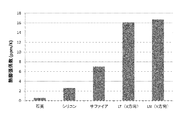
- FIG. 5 is a graph showing the thermal expansion coefficients of various materials in comparison. Among these, silicon has a small coefficient of thermal expansion, is easy to cleave, has a high thermal conductivity, and is excellent in workability, so that it appears to be an excellent balanced selection.
- Si is not an insulator like the other materials (quartz, sapphire, etc.) shown in FIG.
- a thin piezoelectric material such as LT
- Q value resonance sharpness
- Si silicon
- Ordinary Si is produced by the CZ method (Czochralski method). At this time, the single crystal ingot is pulled up from the molten Si in the quartz crucible. At this time, it is difficult to completely prevent oxygen from entering the quartz crucible.
- the FZ method (Floating-Zone method) that does not use a quartz crucible for growth is desirable for producing high-resistance Si.
- the FZ method has problems that it is difficult to increase the diameter (150 mm ⁇ at the maximum) and that the productivity is lower than that of the normal CZ method. Further, not only the productivity of the manufacturing process but also the problem of supply that polysilicon having few impurities must be carefully selected as a material greatly affects the overall productivity of the FZ method.
- Patent Document 1 discloses a method using the CZ method without using the FZ method, which is a factor of low productivity. That is, by applying a magnetic field (Magnetic Field Applied CZ: MCZ method), the convection of the melt is suppressed when growing a single crystal silicon ingot, and oxygen contamination from the quartz crucible is prevented as much as possible. High resistance is achieved by precipitating oxygen by a special heat treatment. However, since special heat treatment for promoting oxygen precipitation is required, it is difficult to fundamentally improve productivity, although not as much as the FZ method.
- MCZ method Magnetic Field Applied CZ
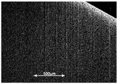
- FIGS. 6 and 7 show optical micrographs of slips generated after heat treatment at 300 ° C. on a wafer in which an LT (20 ⁇ m thickness) and high resistance (> 1000 ⁇ cm) FZ wafer (oxygen concentration is less than 1 ppma) are bonded. .
- FIG. 6 is a photograph near the outer periphery of the substrate
- FIG. 7 is a photograph near 5 mm from the outer periphery of the substrate.
- the method for measuring dissolved oxygen is based on JEIDA-61-2000, which is a standard method for measuring the atomic concentration of interstitial oxygen using infrared rays. This method measures 1106 cm ⁇ 1 , an absorption peak characteristic of interstitial oxygen.
- a JIR-6500 Fourier transform infrared spectrometer (FT-IR) manufactured by JEOL Ltd. was used as a measuring apparatus. Multiplying the absorption coefficient ⁇ obtained here by the coefficient 6.28 is the interstitial oxygen concentration (ppma).
- the interstitial oxygen concentration obtained by this method is simply referred to as “oxygen concentration”.
- An object of the present invention is to provide a composite substrate capable of maintaining high resistance after a process at 300 ° C. and a method for manufacturing the composite substrate.
- SAW devices such as LT and LT / Si do not require a high-temperature process (such as gate oxidation) like the semiconductor CMOS process, and the maximum temperature is about 300 ° C. at the maximum. If the high resistance is maintained up to this temperature, there is no problem in characteristics. Therefore, the inventors have arrived at the idea that a Si substrate that can maintain a high resistance up to about 300 ° C. may be used as a support substrate.
- a composite substrate according to the present invention is formed by bonding a silicon (Si) wafer having an interstitial oxygen concentration of 2 to 10 ppma to a piezoelectric material substrate as a support substrate, and bonding the piezoelectric material substrate after bonding. It is produced by thinning.
- the piezoelectric material substrate may be a lithium tantalate wafer (LT) substrate or a lithium niobate (LN) substrate.
- LT lithium tantalate wafer
- LN lithium niobate
- the composite substrate may have an intervening layer between the piezoelectric material substrate and the silicon wafer.
- the intervening layer may include any of a silicon oxide film, a silicon nitride film, silicon oxynitride (SiON), and amorphous silicon.
- the intervening layer may be thermally oxidized silica.
- the intervening layer may be formed by chemical vapor deposition (CVD) or physical vapor deposition (PVD), or may be formed by applying a silicone-based oil.
- CVD chemical vapor deposition
- PVD physical vapor deposition
- the intervening layer is formed by applying a silicone-based oil, the oil may contain perhydropolysilazane or methyltrimethoxysilane.
- a surface activation treatment may be performed on one or both of the piezoelectric material substrate and the silicon wafer before bonding.
- the surface activation treatment may be performed using a vacuum ion beam or a plasma activation method.
- the composite substrate manufacturing method includes a step of preparing a piezoelectric material substrate and a silicon (Si) wafer having an interstitial oxygen concentration of 2 to 10 ppma as a support substrate. A step of bonding the piezoelectric material substrate and the silicon wafer, and a step of thinning the piezoelectric material substrate after the bonding step.
- the piezoelectric material substrate may be a lithium tantalate wafer (LT) substrate or a lithium niobate (LN) substrate.
- LT lithium tantalate wafer
- LN lithium niobate
- the intervening layer may include any one of a silicon oxide film, a silicon nitride film, silicon oxynitride (SiON), and amorphous silicon.
- the silicon wafer may be thermally oxidized.
- the intervening layer may be formed by chemical vapor deposition (CVD) or physical vapor deposition (PVD).
- the intervening layer may be formed by applying silicone oil.
- the silicone oil may contain perhydropolysilazane or methyltrimethoxysilane.
- the present invention it is preferable to further include a step of performing a surface activation process on one or both of the piezoelectric material substrate and the silicon wafer before the bonding step.
- the surface activation treatment may be performed using a vacuum ion beam or a plasma activation method. By these surface activation treatments, the bonding strength can be increased.
- FIG. 1 is a schematic cross-sectional view illustrating a composite substrate according to an embodiment.
- 10 is a graph showing the results of Example 2.
- 10 is a graph showing the results of Example 3. It is a graph which compares and shows the thermal expansion coefficient of various materials. It is the optical microscope photograph of the slip which arose after performing the heat processing in the outer periphery vicinity of Si substrate. It is the optical microscope photograph of the slip which arose after heat processing in 5 mm vicinity from the outer periphery of Si substrate.
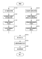
- the composite substrate 1 of the present embodiment is manufactured through a process in which the supporting substrate 10 and the piezoelectric material substrate 20 are each subjected to a pre-bonding process as necessary, and then both the substrates are bonded together. Below, the manufacturing method is demonstrated with reference to the flowchart shown in FIG.
- the support substrate 10 is prepared (step S100).
- a silicon (Si) wafer having an interstitial oxygen concentration of 2 to 10 ppma is used as the support substrate 10.
- the Si wafer used as the support substrate 10 is cut out from a single crystal ingot of Si manufactured by the FZ method, the MCZ method, or the CZ method.
- an intervening layer 31 is formed on the surface of the support substrate 10 as necessary (step S120).
- the material of the intervening layer 31 may include any of a silicon oxide film, a silicon nitride film, silicon oxynitride (SiON), and amorphous silicon.
- the intervening layer 31 can be formed, for example, as a thermally oxidized silica film obtained by thermally oxidizing a Si wafer. Thermally oxidized silica has a property that it is dense, has few impurities, and can absorb a certain amount of gas since it is grown at a high temperature.
- the intervening layer 31 may be formed by other methods.
- the intervening layer 31 may be formed by depositing an appropriate material as the intervening layer by chemical vapor deposition (CVD) such as plasma CVD.
- the intervening layer 31 may be deposited by using a material suitable as an intervening layer by physical vapor deposition (PVD).
- the intervening layer 31 may be formed by applying silicone oil.
- the silicone oil to be applied may contain perhydropolysilazane or methyltrimethoxysilane. Silicone oil may be applied by spin coating.
- the surface to be bonded to the piezoelectric material substrate 20 is flattened as necessary (step S140).
- the degree of planarization is preferably such that the surface roughness Ra (arithmetic mean roughness) is 0.3 nm or less.
- This planarization may be performed by chemical mechanical polishing.
- the intervening layer 31 is not provided on the support substrate 10, the support substrate 10 itself is planarized.
- the surface of the intervening layer 31 is planarized.
- the characteristics of the composite substrate 1 do not depend on the initial surface roughness of the support substrate 10 serving as a base.
- the initial surface roughness of the support substrate 10 may be 150 nm or more in terms of Ra.
- the flattening step may be omitted.
- the support substrate 10 having a mirror-finished surface is used and the intervening layer 31 is formed by thermal oxidation, the surface of the intervening layer 31 also becomes a mirror surface like the base, so this flattening step is unnecessary. is there.
- the surfaces to be bonded (that is, the surface of the support substrate 10 when the intervening layer 31 is not provided, and the interposition layer 31 when the intervening layer 31 is provided are provided as necessary.
- the surface is activated (step S160).
- the surface activation treatment may be any one of ozone water treatment, UV ozone treatment, ion beam treatment, and plasma treatment, for example.
- the piezoelectric material substrate 20 is prepared (step S200).
- the piezoelectric material substrate 20 is a substrate of a piezoelectric material such as lithium tantalate (LT) or lithium niobate (LN), and is preferably a single crystal substrate of these piezoelectric materials.
- LT lithium tantalate
- LN lithium niobate
- an intervening layer 32 is formed on the surface of the piezoelectric material substrate 20 as necessary (step S220).
- the material of the intervening layer 32 may include any of a silicon oxide film, a silicon nitride film, silicon oxynitride (SiON), and amorphous silicon.
- the intervening layer 32 can be formed by the following method. That is, the intervening layer 32 may be formed by depositing an appropriate material as the intervening layer by chemical vapor deposition (CVD) such as plasma CVD. Further, the intervening layer 32 may be formed by depositing a material suitable as an intervening layer by physical vapor deposition (PVD). Alternatively, the intervening layer 32 may be formed by applying a silicone-based oil. The silicone oil to be applied may contain perhydropolysilazane or methyltrimethoxysilane. Silicone oil may be applied by spin coating.
- the surface to be bonded to the support substrate 10 is flattened as necessary (step S240).
- the degree of planarization is preferably such that the surface roughness Ra (arithmetic mean roughness) is 0.3 nm or less. This planarization may be performed by chemical mechanical polishing.
- the intervening layer 32 is not provided on the piezoelectric material substrate 20, the piezoelectric material substrate 20 itself is planarized. Further, when the intervening layer 32 is provided on the piezoelectric material substrate 20, the surface of the intervening layer 32 is flattened.
- the characteristics of the composite substrate 1 do not depend on the initial surface roughness of the piezoelectric material substrate 20 serving as a base.
- the initial surface roughness of the piezoelectric material substrate 20 may be 150 nm or more in terms of Ra.
- the surface to be bonded (that is, the surface of the piezoelectric material substrate 20 when the intervening layer 32 is not provided, or the intervening layer 32 when the intervening layer 31 is provided, as necessary.
- the surface is activated (step S260).
- the surface activation treatment may be any of ozone water treatment, UV ozone treatment, ion beam treatment (for example, vacuum ion beam treatment), and plasma treatment, for example.
- step S300 The support substrate 10 and the piezoelectric material substrate 20 processed as described above are bonded together (step S300). At that time, it is preferable to increase the bonding strength by heating to a low temperature.
- the heating temperature at this low temperature is preferably about 100 ° C., and the heating time is preferably about 24 hours.
- the piezoelectric material substrate 20 is thinned by grinding and polishing as necessary (step S320). For example, the piezoelectric material substrate 20 is thinned until the thickness becomes about 20 ⁇ m. Thereafter, if necessary, additional heat treatment may be performed to strengthen the bonding force (step S340).
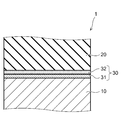
- FIG. 2 is a schematic cross-sectional view of the composite substrate 1 according to this embodiment.
- the intervening layer 31 provided on the support substrate 10 and / or the intervening layer 32 provided on the piezoelectric material substrate 20 becomes an intervening layer 30 sandwiched between the piezoelectric material substrate 20 and the support substrate 10.
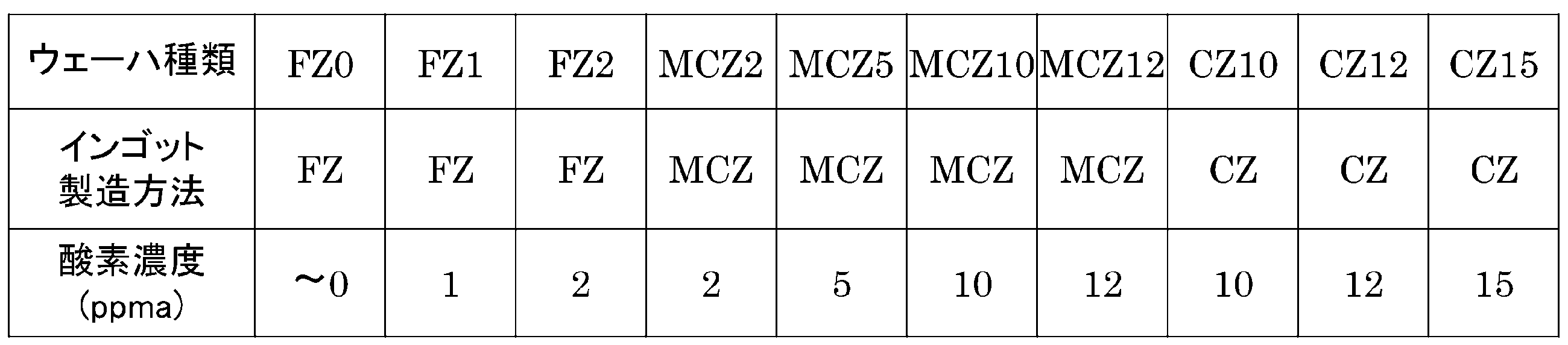
- Example 1 Ten types of 150 mm ⁇ Si wafers (thickness 625 ⁇ m, P-type, resistivity around 1100 ⁇ cm) were prepared, and 150 mm ⁇ LT wafers (thickness 250 ⁇ m) were bonded together. Table 1 shows the manufacturing method and oxygen concentration of the single crystal ingot for each of the 10 types of prepared Si wafers.
- the type of wafer is represented by a combination of a single crystal ingot manufacturing method and an oxygen concentration value. For example, a 1 ppma wafer manufactured by the FZ method is described as “FZ1”.
- the surface roughness of the Si wafer and the LT wafer to be bonded together was confirmed to be 0.3 nm or less in Ra (arithmetic average roughness).
- the bonding was performed by a room temperature bonding method using a vacuum ion beam.
- the LT wafer was thinned to 20 ⁇ m by grinding and polishing.
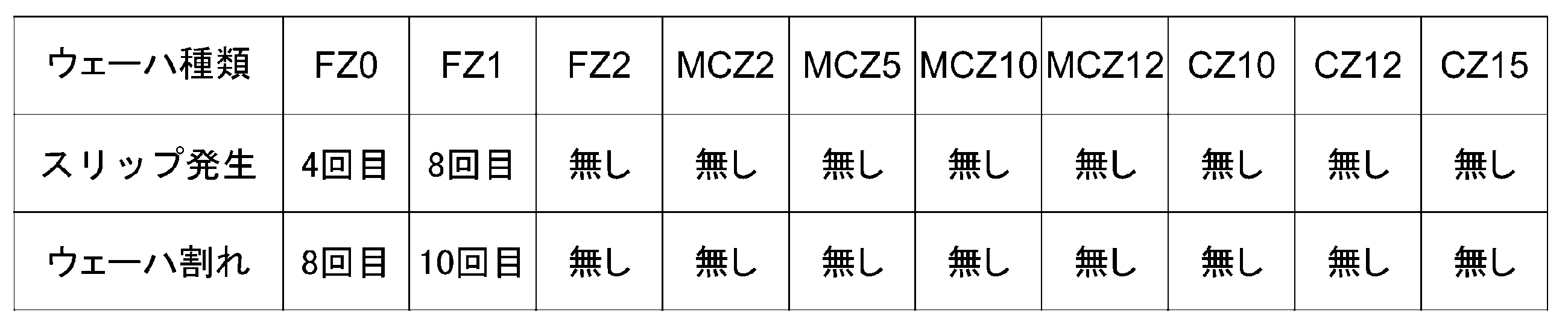
- the composite substrate wafer bonded in this manner was reciprocated 10 times between a 300 ° C. hot plate and a cooling stage, and then the occurrence of slip and the cracking state of the wafer were observed.
- Table 2 From this result, it was found that the occurrence of slip and wafer cracking can be prevented if the oxygen concentration of the Si wafer is 2 ppma or more. Similar results were obtained when LN was used instead of LT.
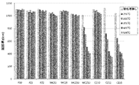
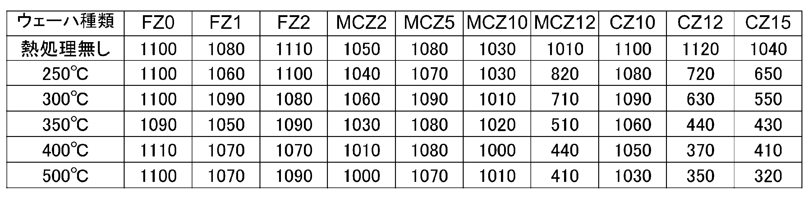
- Example 2 Ten types of Si wafers similar to Example 1 were prepared, and heat treatment at 250 ° C., 300 ° C., 350 ° C., 400 ° C., 450 ° C., and 500 ° C. was performed in a nitrogen atmosphere for 1 hour. The results of measuring the resistivity before and after the heat treatment are shown in Table 3 and FIG. As a result, if the oxygen concentration of the Si wafer is 10 ppma or less, the resistivity change is not affected by heat treatment up to 350 ° C., which is considered to be the maximum temperature of the LT device manufacturing process, regardless of the Si single crystal ingot manufacturing method. It turns out that there is almost nothing.
- Example 3 A resonator was fabricated using the wafers of the 10 types of composite substrates obtained in Example 1, and the Q value was measured.
- the maximum temperature of the manufacturing process of the resonator which is the LT device is about 350 ° C.
- the surviving portion that is, the portion having a size that enables the manufacture of the device
- the device was produced at the portion where the slip did not occur, and measurement was performed.
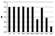
- the results of the Q value are shown in Table 4 and FIG. From this result, there was no deterioration of the characteristics when the oxygen concentration of the Si wafer was 10 ppma or less, and deterioration of the characteristics was observed when the oxygen concentration was larger than 10 ppma. This result was found to be consistent with the change in resistivity in Example 2.
- Example 4 Ten types of 150 mm ⁇ Si wafers (thickness: 625 ⁇ m) similar to those in Example 1 were prepared, and a 100 nm thermal oxide film was grown. The conditions for thermal oxidation are 700 ° C. input and 1000 ° C. dry oxidation. Moreover, a 150 mm ⁇ LT wafer (thickness 250 ⁇ m) was prepared. Surface activation was performed by plasma activation on both the Si wafer and the LT wafer on which the thermal oxide film was grown, and the both wafers were bonded together. After bonding, heat treatment was performed at 100 ° C. for 24 hours. It was confirmed that the surface roughness of each wafer before bonding was Ra of 0.3 nm or less.
- the LT wafer was thinned to 20 ⁇ m by grinding and polishing. These wafers were reciprocated 10 times between a 300 ° C. hot plate and a cooling stage, and then the occurrence of slips and the cracking state of the wafers were observed. The results are shown in Table 5. From this result, it was found that slip generation and wafer cracking can be prevented if the oxygen concentration of the Si wafer is 2 ppma or more. This result is almost the same as in Example 1. Regardless of the presence or absence of the thermal oxide film, the occurrence of slip and wafer cracking depend on the oxygen concentration of the Si wafer, and it is important that the oxygen concentration is 2 ppma or more. There was found.
- Example 5 Ten types of Si wafers similar to those in Example 1 were prepared, and thermal oxidation was performed in the same manner as in Example 4. Thus, about the Si wafer which provided the thermal oxide film, the conditions of additional heat processing were changed and the resistivity before and after additional heat processing was measured. There were six additional heat treatment conditions: no additional heat treatment, 250 ° C., 300 ° C., 350 ° C., 400 ° C., and 500 ° C. The additional heat treatment was performed in a nitrogen atmosphere for 1 hour. The resistivity was measured before and after that. The result of the measurement was almost the same as in Example 2. It was found that there was almost no change in resistivity even when heat treatment up to 350 ° C. was performed if the oxygen concentration was 10 ppma or less. It was found that even when using a Si wafer provided with a thermal oxide film, it can be used without problems such as a decrease in resistivity by avoiding treatment in the thermal donor generation temperature range (400 to 600 ° C.).
- Example 6 Ten types of 150 mm ⁇ Si wafers (thickness: 625 ⁇ m) similar to Example 1 were prepared, and a 200 nm plasma CVD oxide film was deposited near room temperature. After depositing the oxide film, it was polished for mirroring. Moreover, a 150 mm ⁇ LT wafer (thickness 250 ⁇ m) was prepared. Surface activation was performed by plasma activation on both the Si wafer and the LT wafer on which the oxide film was deposited, and the both wafers were bonded together. After bonding, heat treatment was performed at 100 ° C. for 24 hours. It was confirmed that the surface roughness of both wafers before bonding was Ra of 0.3 nm or less. As a result of conducting the same heat resistance experiment as in Example 1, the same tendency as in Example 1 was shown. From this result, it was found that the effect of the present invention can be obtained without depending on the method of forming the oxide film.
- Example 7 Ten types of 150 mm ⁇ Si wafers (thickness: 625 ⁇ m) and 150 mm ⁇ LT wafers (thickness: 250 ⁇ m) were prepared in the same manner as in Example 1, and a 200 nm plasma CVD oxide film was deposited on the LT wafer near room temperature. After deposition, polishing was performed for mirroring. Surface activation was performed by plasma activation on both the Si wafer and the LT wafer on which the oxide film was deposited, and the both wafers were bonded together. After bonding, heat treatment was performed at 100 ° C. for 24 hours. It was confirmed that the surface roughness of both wafers before bonding was Ra of 0.3 nm or less.
- Example 1 The same heat resistance experiment as in Example 1 was performed, but the results showed exactly the same tendency as in Example 1. From this result, it has been found that the effect of the present invention can be obtained without depending on the location where the oxide film is formed (that is, whether the Si wafer or the LT wafer is provided with an intervening layer such as an oxide film).
- Example 8 Ten types of 150 mm ⁇ Si wafers (thickness: 625 ⁇ m) and 150 mm ⁇ LT wafers (thickness: 250 ⁇ m) having the same surface as in Example 1 were prepared. Deposited on the wafer near room temperature. After deposition, polishing was performed for mirroring. Surface activation was performed by plasma activation on both the Si wafer and the LT wafer on which the oxide film was deposited, and the both wafers were bonded together. After bonding, heat treatment was performed at 100 ° C. for 24 hours. It was confirmed that the surface roughness of both wafers before bonding was Ra of 0.3 nm or less. The results showed exactly the same tendency as in Example 1.
- Example 9 Ten types of 150 mm ⁇ Si wafers (thickness: 625 ⁇ m) similar to those in Example 1 were prepared, and a 200 nm plasma CVD nitride (SiN) film was deposited near room temperature. After deposition, polishing was performed for mirroring. Moreover, a 150 mm ⁇ LT wafer (thickness 250 ⁇ m) was prepared. Surface activation was performed by plasma activation on both the Si wafer and the LT wafer on which the nitride film was deposited, and the both wafers were bonded together. After bonding, heat treatment was performed at 100 ° C. for 24 hours. It was confirmed that the surface roughness of both wafers before bonding was Ra of 0.3 nm or less.
- SiN plasma CVD nitride
- Example 1 The results showed exactly the same tendency as in Example 1. It has been found that this method does not depend on the oxide film forming method. Similarly, similar results were obtained when amorphous Si (formed by physical vapor deposition (PVD method)) or SiON was deposited on the Si wafer. From this result, it was found that the effects of the present invention can be obtained regardless of the type (material) of the intervening layer. The same result was obtained when the silicon oxide film was formed by spin coating silicone oil such as perhydropolysilazane or methyltrimethoxysilane.
- PVD method physical vapor deposition
Landscapes
- Physics & Mathematics (AREA)
- Acoustics & Sound (AREA)
- Engineering & Computer Science (AREA)
- Manufacturing & Machinery (AREA)
- Chemical & Material Sciences (AREA)
- Materials Engineering (AREA)
- Crystals, And After-Treatments Of Crystals (AREA)
- Surface Acoustic Wave Elements And Circuit Networks Thereof (AREA)
Abstract
Description
はじめに、支持基板10を用意する(ステップS100)。支持基板10としては、格子間酸素濃度が2から10ppmaのシリコン(Si)ウェーハを用いる。支持基板10として用いるSiウェーハは、FZ法、MCZ法、もしくはCZ法にて製造されたSiの単結晶インゴットから切り出される。
はじめに、圧電材料基板20を用意する(ステップS200)。圧電材料基板20は、タンタル酸リチウム(LT)やニオブ酸リチウム(LN)などの圧電材料の基板であり、好ましくは、これらの圧電材料の単結晶基板である。
上記のように処理した支持基板10と圧電材料基板20とを貼り合わせる(ステップS300)。その際、低温に加熱して接合強度を高めるとよい。この低温での加熱温度は例えば100℃程度とするとよく、加熱時間は24時間程度とするとよい。
10種類の150mmΦのSiウェーハ(厚さ625μm、P型、抵抗率1100Ωcm前後)を用意し、150mmΦのLTウェーハ(厚さ250μm)を貼り合わせ行った。用意した10種類のSiウェーハのそれぞれについて、単結晶インゴットの製造方法と酸素濃度を表1に示す。なお、ウェーハの種類は、単結晶インゴットの製造方法と酸素濃度の数値との組み合わせにより表した。例えば、FZ法で製造した1ppmaのウェーハは「FZ1」と記載した。

実施例1と同様の10種類のSiウェーハを用意し、250℃、300℃、350℃、400℃、450℃、500℃の熱処理を窒素雰囲気で1時間行った。熱処理の前後で抵抗率の測定を行った結果を表3及び図3に示す。この結果、Siウェーハの酸素濃度が10ppma以下であれば、Si単結晶インゴットの製造方法によらず、LTデバイス製造プロセスの最高温度と考えられる350℃までの熱処理を行っても抵抗率の変化はほとんど無いことが判明した。
実施例1にて得られた10種類の複合基板のウェーハを用いて共振器を作製し、Q値を測定した。LTデバイスである共振器の製造プロセスの最高温度は350℃程度である。割れたウェーハについては生き残った箇所(つまり、デバイスの製造が可能な程度のサイズの部位)を用い、スリップの出たウェーハについてはスリップの出ていない部分でデバイスを作製し、測定を行った。Q値の結果を表4及び図4に示す。この結果からSiウェーハの酸素濃度が10ppma以下のものに関しては特性の劣化が無く、10ppmaよりも大きいものは特性の劣化が観察された。この結果は、実施例2における抵抗率の変化と整合していることが判明した。

実施例1と同様の10種類の150mmΦのSiウェーハ(厚さ625μm)を用意し、100nmの熱酸化膜を成長させた。熱酸化の条件は700℃投入、1000℃のドライ酸化である。また、150mmΦのLTウェーハ(厚さ250μm)を用意した。熱酸化膜を成長させたSiウェーハ及びLTウェーハの双方にプラズマ活性化により表面活性化を行い、両ウェーハを貼り合わせた。貼り合わせ後は100℃で24時間の熱処理を施した。貼り合わせ前の各ウェーハの表面粗さは、いずれもRaで0.3nm以下であることを確認した。
実施例1と同様の10種類のSiウェーハを用意し、実施例4と同様の方法で熱酸化を施した。このようにして熱酸化膜を設けたSiウェーハについて、追加熱処理の条件を変化させ、追加熱処理の前後における抵抗率を測定した。追加熱処理の条件は、追加熱処理無し、250℃、300℃、350℃、400℃、500℃の6通りであり、追加熱処理は窒素雰囲気で1時間行った。その前後で抵抗率の測定を行った。測定の結果は実施例2とほぼ同様となり、酸素濃度が10ppma以下であれば、350℃までの熱処理を行っても抵抗率の変化はほとんど無いことが判明した。熱酸化膜を設けたSiウェーハを用いた場合でもサーマルドナー発生温度域(400~600℃)での処理を避けることで、抵抗率の低下などの問題無く使用できることが判明した。
実施例1と同様の10種類の150mmΦのSiウェーハ(厚さ625μm)を用意し、200nmのプラズマCVD酸化膜を室温近傍で堆積した。酸化膜を堆積した後、鏡面化のために研磨を行った。また、150mmΦのLTウェーハ(厚さ250μm)を用意した。酸化膜を堆積したSiウェーハ及びLTウェーハの双方にプラズマ活性化により表面活性化を行い、両ウェーハを貼り合わせた。貼り合わせ後は100℃で24時間の熱処理を施した。貼り合わせ前の両ウェーハの表面粗さは、いずれもRaで0.3nm以下であることを確認した。実施例1と同様の熱耐性実験を行った結果、実施例1と同じ傾向を示した。この結果から、酸化膜の形成方法には依存せず、本発明の効果が得られることが判明した。
実施例1と同様の10種類の150mmΦのSiウェーハ(厚さ625μm)と150mmΦのLTウェーハ(厚さ250μm)を用意し、200nmのプラズマCVD酸化膜をLTウェーハ上に室温近傍で堆積した。堆積の後に鏡面化のために研磨を行った。Siウェーハ及び酸化膜を堆積したLTウェーハの双方にプラズマ活性化により表面活性化を行い、両ウェーハを貼り合わせた。貼り合わせ後は100℃で24時間の熱処理を施した。貼り合わせ前の両ウェーハの表面粗さは、いずれもRaで0.3nm以下であることを確認した。実施例1と同様の熱耐性実験を行ったが、結果は実施例1と全く同じ傾向を示した。この結果から、酸化膜の形成箇所(すなわち、SiウェーハとLTウェーハのどちらに酸化膜等の介在層を設けるか)には依存せず、本発明の効果が得られることが判明した。
実施例1と同様の10種類の150mmΦのSiウェーハ(厚さ625μm)と、表面の荒れた(Ra=160nm)150mmΦのLTウェーハ(厚さ250μm)を用意し、5μmのプラズマCVD酸化膜をLTウェーハ上に室温近傍に堆積した。堆積の後に鏡面化のために研磨を行った。Siウェーハ及び酸化膜を堆積したLTウェーハの双方にプラズマ活性化により表面活性化を行い、両ウェーハを貼り合わせた。貼り合わせ後は100℃で24時間の熱処理を施した。貼り合わせ前の両ウェーハの表面粗さは、いずれもRaで0.3nm以下であることを確認した。結果は実施例1と全く同じ傾向を示した。この結果から、介在層を形成するLTウェーハの初期面粗さには依存せず本発明の効果が得られることが判明した。同様に表面の荒れたSi(Ra=175nm)を用い、同様の実験をした場合も実施例1と同様の結果を示した。また、LTとSi双方の貼り合わせ面が荒れているものに介在層を設けた場合も同様の結果を示した。よって、LTとSiの間に介在層を設ける場合は、LTもしくはSiの貼り合わせ面の片方、もしくは両面が鏡面化されていなくとも本方法の効果には影響が無い事が判明した。
実施例1と同様の10種類の150mmΦのSiウェーハ(厚さ625μm)を用意し、200nmのプラズマCVD窒化(SiN)膜を室温近傍で堆積した。堆積の後に鏡面化のために研磨を行った。また、150mmΦのLTウェーハ(厚さ250μm)を用意した。窒化膜を堆積したSiウェーハ及びLTウェーハの双方にプラズマ活性化により表面活性化を行い、両ウェーハを貼り合わせた。貼り合わせ後は100℃で24時間の熱処理を施した。貼り合わせ前の両ウェーハの表面粗さは、いずれもRaで0.3nm以下であることを確認した。結果は実施例1と全く同じ傾向を示した。本方法は酸化膜の形成方法には依存しないことが判明した。また、同様にSiウェーハの上にアモルファスSi(物理気相成長法(PVD法)で形成)やSiONなどを堆積した場合も同様の結果となった。この結果から、介在層の種類(材質)によらず本発明の効果が得られることが判明した。またシリコン酸化膜をパーヒドロポリシラザンやメチルトリメトキシシランなどのシリコーンオイルをスピンコートして形成した場合も同様の結果となった。
10…支持基板
20…圧電材料基板
30、31、32…介在層
Claims (24)
- 圧電材料基板に、格子間酸素濃度が2から10ppmaのシリコン(Si)ウェーハを支持基板として貼り合わせ、貼り合わせ後に前記圧電材料基板を薄化することにより作製される複合基板。
- 前記圧電材料基板は、タンタル酸リチウムウェーハ(LT)基板又はニオブ酸リチウム(LN)基板であることを特徴とする請求項1に記載の複合基板。
- 前記シリコンウェーハは、FZ法、MCZ法、及びCZ法の何れかにより製造された結晶から切り出されたものであることを特徴とする請求項1または2に記載の複合基板。
- 前記圧電材料基板と前記シリコンウェーハとの間に介在層を有することを特徴とする請求項1から3の何れか1項に記載の複合基板。
- 前記介在層が、シリコン酸化膜、シリコン窒化膜、シリコンオキシナイトライド(SiON)、及びアモルファスシリコンのいずれかを含むことを特徴とする請求項4に記載の複合基板。
- 前記介在層が熱酸化シリカであることを特徴とする請求項4に記載の複合基板。
- 前記介在層が化学気相成長(CVD)又は物理気相成長(PVD)で形成されることを特徴とする請求項4または5に記載の複合基板。
- 前記介在層がシリコーン系のオイルを塗布することで形成されることを特徴とする請求項4または5に記載の複合基板。
- 前記シリコーン系のオイルがパーヒドロポリシラザン又はメチルトリメトキシシランを含有することを特徴とする請求項8に記載の複合基板。
- 前記圧電材料基板及び前記シリコンウェーハの少なくとも一方の表面が非鏡面とされ、当該非鏡面の表面上に貼り合せ前に前記介在層が予め設けられることを特徴とすることを特徴とする請求項4から9の何れか1項に記載の複合基板。
- 前記圧電材料基板及び前記シリコンウェーハの片方もしくは双方に対し、貼り合わせの前に表面活性化処理を施すことを特徴とする請求項1から10のいずれか1項に記載の複合基板。
- 前記表面活性化処理が、真空イオンビーム又はプラズマ活性化法を用いて行われることを特徴とする請求項11に記載の複合基板。
- 圧電材料基板を用意する工程と、
支持基板として格子間酸素濃度が2から10ppmaのシリコン(Si)ウェーハを用意する工程と、
前記圧電材料基板と前記シリコンウェーハとを貼り合わせる工程と、
前記貼り合わせる工程の後で、前記圧電材料基板を薄化する工程とを含む
複合基板の製造方法。 - 前記圧電材料基板は、タンタル酸リチウムウェーハ(LT)基板もしくはニオブ酸リチウム(LN)基板であることを特徴とする請求項13に記載の複合基板の製造方法。
- 前記シリコンウェーハは、FZ法、MCZ法、及びCZ法の何れかにより製造された結晶から切り出されたものであることを特徴とする請求項13または14に記載の複合基板の製造方法。
- 前記貼り合わせる工程の前に、前記圧電材料基板及び前記シリコンウェーハの何れか又は両方の表面に、介在層を設ける工程をさらに有することを特徴とする請求項13から15の何れか1項に記載の複合基板の製造方法。
- 前記介在層が、シリコン酸化膜、シリコン窒化膜、シリコンオキシナイトライド(SiON)、及びアモルファスシリコンのいずれかを含むことを特徴とする請求項16に記載の複合基板の製造方法。
- 前記介在層を設ける工程において、前記シリコンウェーハを熱酸化することを特徴とする請求項16に記載の複合基板の製造方法。
- 前記介在層を設ける工程において、前記介在層を化学気相成長(CVD)又は物理気相成長(PVD)で形成することを特徴とする請求項16または17に記載の複合基板の製造方法。
- 前記介在層を設ける工程において、シリコーン系のオイルを塗布することにより前記介在層を形成することを特徴とする請求項16または17に記載の複合基板の製造方法。
- 前記シリコーン系のオイルがパーヒドロポリシラザン又はメチルトリメトキシシランを含有することを特徴とする請求項20に記載の複合基板の製造方法。
- 前記圧電材料基板及び前記シリコンウェーハの少なくとも一方の表面が非鏡面とされ、当該非鏡面の表面上に貼り合せ前に前記介在層が予め設けられることを特徴とする請求項16から21の何れか1項に記載の複合基板の製造方法。
- 前記貼り合わせる工程の前に、前記圧電材料基板及び前記シリコンウェーハの片方もしくは双方に対し、表面活性化処理を施す工程をさらに備えることを特徴とする請求項13から22のいずれか1項に記載の複合基板の製造方法。
- 前記表面活性化処理が、真空イオンビーム又はプラズマ活性化法を用いて行われることを特徴とする請求項22に記載の複合基板の製造方法。
Priority Applications (5)
| Application Number | Priority Date | Filing Date | Title |
|---|---|---|---|
| US16/475,528 US11804818B2 (en) | 2017-01-18 | 2017-12-06 | Method of manufacturing composite substrate |
| EP17892974.1A EP3573088B1 (en) | 2017-01-18 | 2017-12-06 | Method of manufacturing a composite substrate |
| KR1020197021403A KR102578946B1 (ko) | 2017-01-18 | 2017-12-06 | 복합 기판 및 복합 기판의 제조 방법 |
| CN201780081147.XA CN110140192B (zh) | 2017-01-18 | 2017-12-06 | 复合基板和复合基板的制造方法 |
| US18/370,612 US12676589B2 (en) | 2017-01-18 | 2023-09-20 | Composite substrate |
Applications Claiming Priority (2)
| Application Number | Priority Date | Filing Date | Title |
|---|---|---|---|
| JP2017006351A JP6696917B2 (ja) | 2017-01-18 | 2017-01-18 | 複合基板の製造方法 |
| JP2017-006351 | 2017-01-18 |
Related Child Applications (2)
| Application Number | Title | Priority Date | Filing Date |
|---|---|---|---|
| US16/475,528 A-371-Of-International US11804818B2 (en) | 2017-01-18 | 2017-12-06 | Method of manufacturing composite substrate |
| US18/370,612 Division US12676589B2 (en) | 2017-01-18 | 2023-09-20 | Composite substrate |
Publications (1)
| Publication Number | Publication Date |
|---|---|
| WO2018135163A1 true WO2018135163A1 (ja) | 2018-07-26 |
Family
ID=62908414
Family Applications (1)
| Application Number | Title | Priority Date | Filing Date |
|---|---|---|---|
| PCT/JP2017/043767 Ceased WO2018135163A1 (ja) | 2017-01-18 | 2017-12-06 | 複合基板および複合基板の製造方法 |
Country Status (7)
| Country | Link |
|---|---|
| US (2) | US11804818B2 (ja) |
| EP (1) | EP3573088B1 (ja) |
| JP (1) | JP6696917B2 (ja) |
| KR (1) | KR102578946B1 (ja) |
| CN (1) | CN110140192B (ja) |
| TW (1) | TWI829629B (ja) |
| WO (1) | WO2018135163A1 (ja) |
Cited By (3)
| Publication number | Priority date | Publication date | Assignee | Title |
|---|---|---|---|---|
| WO2020044925A1 (ja) * | 2018-08-30 | 2020-03-05 | 信越化学工業株式会社 | 複合基板および複合基板の製造方法 |
| WO2026048449A1 (ja) * | 2024-08-30 | 2026-03-05 | グローバルウェーハズ・ジャパン株式会社 | 複合基板の製造方法、複合基板、および弾性波デバイス |
| WO2026048189A1 (ja) * | 2024-08-27 | 2026-03-05 | 日本碍子株式会社 | 複合基板の製造方法 |
Families Citing this family (13)
| Publication number | Priority date | Publication date | Assignee | Title |
|---|---|---|---|---|
| JP6696917B2 (ja) | 2017-01-18 | 2020-05-20 | 信越化学工業株式会社 | 複合基板の製造方法 |
| US10943813B2 (en) | 2018-07-13 | 2021-03-09 | Globalwafers Co., Ltd. | Radio frequency silicon on insulator wafer platform with superior performance, stability, and manufacturability |
| KR102409618B1 (ko) * | 2018-08-07 | 2022-06-16 | 지난 징젱 일렉트로닉스 씨오., 엘티디. | 마이크로미터급 단결정 필름 |
| WO2020250491A1 (ja) * | 2019-06-11 | 2020-12-17 | 日本碍子株式会社 | 複合基板、弾性波素子および複合基板の製造方法 |
| CN110581212B (zh) * | 2019-09-20 | 2021-09-24 | 济南晶正电子科技有限公司 | 一种单晶单畴压电薄膜及其制备方法 |
| JP7271458B2 (ja) * | 2020-02-03 | 2023-05-11 | 信越化学工業株式会社 | 複合基板の製造方法 |
| JP7274442B2 (ja) * | 2020-04-02 | 2023-05-16 | 信越化学工業株式会社 | 複合基板およびその製造方法 |
| JP7262415B2 (ja) | 2020-04-03 | 2023-04-21 | 信越化学工業株式会社 | 複合基板およびその製造方法 |
| TWI884167B (zh) | 2020-05-20 | 2025-05-21 | 日商日本碍子股份有限公司 | 電光元件用複合基板 |
| JP6866952B1 (ja) * | 2020-07-29 | 2021-04-28 | 信越半導体株式会社 | 窒化物半導体ウェーハおよび窒化物半導体ウェーハの製造方法 |
| CN111786647B (zh) | 2020-08-07 | 2021-06-15 | 展讯通信(上海)有限公司 | 晶圆级声表面波滤波器与封装方法 |
| TWI806457B (zh) * | 2022-03-01 | 2023-06-21 | 鴻創應用科技有限公司 | 複合基板及其製造方法 |
| CN119421633B (zh) * | 2025-01-06 | 2025-04-18 | 同济大学 | 基于尖晶石陶瓷衬底的异质结构衬底及其制备方法和应用 |
Citations (4)
| Publication number | Priority date | Publication date | Assignee | Title |
|---|---|---|---|---|
| JP2002184960A (ja) * | 2000-12-18 | 2002-06-28 | Shin Etsu Handotai Co Ltd | Soiウェーハの製造方法及びsoiウェーハ |
| US6544656B1 (en) | 1999-03-16 | 2003-04-08 | Shin-Etsu Handotai Co., Ltd. | Production method for silicon wafer and silicon wafer |
| JP2004304622A (ja) * | 2003-03-31 | 2004-10-28 | Fujitsu Media Device Kk | 弾性表面波デバイス及びその製造方法 |
| JP2010045260A (ja) * | 2008-08-15 | 2010-02-25 | Shin-Etsu Chemical Co Ltd | 基板の接合方法並びに3次元半導体装置 |
Family Cites Families (15)
| Publication number | Priority date | Publication date | Assignee | Title |
|---|---|---|---|---|
| JPH0810695B2 (ja) | 1986-10-02 | 1996-01-31 | ソニー株式会社 | 半導体基板の製法 |
| JPH09246129A (ja) | 1996-03-05 | 1997-09-19 | Sumitomo Sitix Corp | 貼り合わせシリコンウエーハの製造方法 |
| US6565652B1 (en) * | 2001-12-06 | 2003-05-20 | Seh America, Inc. | High resistivity silicon wafer and method of producing same using the magnetic field Czochralski method |
| US7105980B2 (en) | 2002-07-03 | 2006-09-12 | Sawtek, Inc. | Saw filter device and method employing normal temperature bonding for producing desirable filter production and performance characteristics |
| JP3774782B2 (ja) * | 2003-05-14 | 2006-05-17 | 富士通メディアデバイス株式会社 | 弾性表面波素子の製造方法 |
| JP2006303940A (ja) * | 2005-04-21 | 2006-11-02 | Nec Tokin Corp | 複合圧電基板及びその製造方法 |
| JP5552889B2 (ja) * | 2010-05-10 | 2014-07-16 | 日立化成株式会社 | プリント配線板用熱硬化性樹脂組成物並びにこれを用いたワニス、プリプレグ及び金属張積層板 |
| JP5814774B2 (ja) * | 2010-12-22 | 2015-11-17 | 日本碍子株式会社 | 複合基板及び複合基板の製造方法 |
| US8536035B2 (en) * | 2012-02-01 | 2013-09-17 | International Business Machines Corporation | Silicon-on-insulator substrate and method of forming |
| JP5861771B2 (ja) | 2012-03-26 | 2016-02-16 | 株式会社村田製作所 | 弾性波装置及びその製造方法 |
| JP6220279B2 (ja) * | 2014-02-04 | 2017-10-25 | 日本碍子株式会社 | 複合基板の研磨方法 |
| WO2016084526A1 (ja) | 2014-11-28 | 2016-06-02 | 株式会社村田製作所 | 弾性波装置 |
| US20170330747A1 (en) * | 2014-12-05 | 2017-11-16 | Shin-Etsu Chemical Co., Ltd. | Composite substrate manufacturing method and composite substrate |
| JP6447439B2 (ja) * | 2015-09-28 | 2019-01-09 | 信越半導体株式会社 | 貼り合わせsoiウェーハの製造方法 |
| JP6696917B2 (ja) * | 2017-01-18 | 2020-05-20 | 信越化学工業株式会社 | 複合基板の製造方法 |
-
2017
- 2017-01-18 JP JP2017006351A patent/JP6696917B2/ja active Active
- 2017-12-06 CN CN201780081147.XA patent/CN110140192B/zh active Active
- 2017-12-06 KR KR1020197021403A patent/KR102578946B1/ko active Active
- 2017-12-06 WO PCT/JP2017/043767 patent/WO2018135163A1/ja not_active Ceased
- 2017-12-06 EP EP17892974.1A patent/EP3573088B1/en active Active
- 2017-12-06 US US16/475,528 patent/US11804818B2/en active Active
-
2018
- 2018-01-17 TW TW107101622A patent/TWI829629B/zh active
-
2023
- 2023-09-20 US US18/370,612 patent/US12676589B2/en active Active
Patent Citations (4)
| Publication number | Priority date | Publication date | Assignee | Title |
|---|---|---|---|---|
| US6544656B1 (en) | 1999-03-16 | 2003-04-08 | Shin-Etsu Handotai Co., Ltd. | Production method for silicon wafer and silicon wafer |
| JP2002184960A (ja) * | 2000-12-18 | 2002-06-28 | Shin Etsu Handotai Co Ltd | Soiウェーハの製造方法及びsoiウェーハ |
| JP2004304622A (ja) * | 2003-03-31 | 2004-10-28 | Fujitsu Media Device Kk | 弾性表面波デバイス及びその製造方法 |
| JP2010045260A (ja) * | 2008-08-15 | 2010-02-25 | Shin-Etsu Chemical Co Ltd | 基板の接合方法並びに3次元半導体装置 |
Non-Patent Citations (2)
| Title |
|---|
| "Dempa Shi rrbun High Technology", November 2012, TAI YO YUDEN CO. , LT D., article "Temperature Corrpensation Technology for SAW Dupl exer Used in RF Front End of Smart phone" |
| "Realize Science and Technology Center", 28 June 1996, article "Science of Silicon", pages: 576 - 582 |
Cited By (4)
| Publication number | Priority date | Publication date | Assignee | Title |
|---|---|---|---|---|
| WO2020044925A1 (ja) * | 2018-08-30 | 2020-03-05 | 信越化学工業株式会社 | 複合基板および複合基板の製造方法 |
| JP2020036212A (ja) * | 2018-08-30 | 2020-03-05 | 信越化学工業株式会社 | 複合基板および複合基板の製造方法 |
| WO2026048189A1 (ja) * | 2024-08-27 | 2026-03-05 | 日本碍子株式会社 | 複合基板の製造方法 |
| WO2026048449A1 (ja) * | 2024-08-30 | 2026-03-05 | グローバルウェーハズ・ジャパン株式会社 | 複合基板の製造方法、複合基板、および弾性波デバイス |
Also Published As
| Publication number | Publication date |
|---|---|
| TWI829629B (zh) | 2024-01-21 |
| JP2018117030A (ja) | 2018-07-26 |
| EP3573088A4 (en) | 2020-12-02 |
| JP6696917B2 (ja) | 2020-05-20 |
| CN110140192B (zh) | 2023-12-15 |
| KR20190100285A (ko) | 2019-08-28 |
| EP3573088A1 (en) | 2019-11-27 |
| US20190386640A1 (en) | 2019-12-19 |
| US12676589B2 (en) | 2026-07-07 |
| TW201832391A (zh) | 2018-09-01 |
| EP3573088B1 (en) | 2026-04-29 |
| US20240022229A1 (en) | 2024-01-18 |
| KR102578946B1 (ko) | 2023-09-14 |
| CN110140192A (zh) | 2019-08-16 |
| US11804818B2 (en) | 2023-10-31 |
Similar Documents
| Publication | Publication Date | Title |
|---|---|---|
| US20240022229A1 (en) | Composite substrate | |
| TWI709197B (zh) | 製造具有電荷捕捉層之高電阻率絕緣體上半導體晶圓之方法 | |
| US10829868B2 (en) | Manufacturing method of SiC composite substrate | |
| TWI698907B (zh) | 貼合式soi晶圓的製造方法 | |
| EP3352197B1 (en) | Method for producing a composite sic substrate | |
| JP7262415B2 (ja) | 複合基板およびその製造方法 | |
| TWI582911B (zh) | 製造絕緣體上矽之晶圓之方法 | |
| JP6288323B2 (ja) | 熱酸化異種複合基板の製造方法 | |
| TWI609434B (zh) | SOS substrate manufacturing method and SOS substrate | |
| CN113421849A (zh) | 一种带绝缘埋层的硅衬底的制备工艺 | |
| WO2015074478A1 (zh) | 低翘曲度的半导体衬底的制备方法 | |
| CN105264641B (zh) | 贴合晶圆的制造方法 | |
| JP2020120128A (ja) | 複合基板 | |
| WO2015074479A1 (zh) | 低翘曲度的半导体衬底及其制备方法 | |
| WO2012105367A1 (ja) | Soiウェーハの製造方法 | |
| JP2011029594A (ja) | Soiウェーハの製造方法及びsoiウェーハ | |
| CN114284135B (zh) | 一种复合衬底的制备方法、复合衬底以及电子元器件 | |
| JP2010040608A (ja) | 貼り合わせsoiウェーハの製造方法 | |
| JP2026045924A (ja) | 複合基板の製造方法、複合基板、および弾性波素子 | |
| JP2026045925A (ja) | 複合基板の製造方法、複合基板、および弾性波素子 | |
| WO2024029217A1 (ja) | 3C-SiC積層基板の製造方法、3C-SiC積層基板及び3C-SiC自立基板 | |
| WO2026048449A1 (ja) | 複合基板の製造方法、複合基板、および弾性波デバイス | |
| WO2021157218A1 (ja) | 複合基板およびその製造方法 |
Legal Events
| Date | Code | Title | Description |
|---|---|---|---|
| 121 | Ep: the epo has been informed by wipo that ep was designated in this application |
Ref document number: 17892974 Country of ref document: EP Kind code of ref document: A1 |
|
| NENP | Non-entry into the national phase |
Ref country code: DE |
|
| ENP | Entry into the national phase |
Ref document number: 20197021403 Country of ref document: KR Kind code of ref document: A |
|
| ENP | Entry into the national phase |
Ref document number: 2017892974 Country of ref document: EP Effective date: 20190819 |
|
| WWG | Wipo information: grant in national office |
Ref document number: 2017892974 Country of ref document: EP |