WO2018155418A1 - 多層配線基板および半導体装置 - Google Patents
多層配線基板および半導体装置 Download PDFInfo
- Publication number
- WO2018155418A1 WO2018155418A1 PCT/JP2018/005932 JP2018005932W WO2018155418A1 WO 2018155418 A1 WO2018155418 A1 WO 2018155418A1 JP 2018005932 W JP2018005932 W JP 2018005932W WO 2018155418 A1 WO2018155418 A1 WO 2018155418A1
- Authority
- WO
- WIPO (PCT)
- Prior art keywords
- adhesive layer
- wiring board
- multilayer wiring
- substrate
- fluororesin
- Prior art date
- Legal status (The legal status is an assumption and is not a legal conclusion. Google has not performed a legal analysis and makes no representation as to the accuracy of the status listed.)
- Ceased
Links
Images
Classifications
-
- H—ELECTRICITY
- H05—ELECTRIC TECHNIQUES NOT OTHERWISE PROVIDED FOR
- H05K—PRINTED CIRCUITS; CASINGS OR CONSTRUCTIONAL DETAILS OF ELECTRIC APPARATUS; MANUFACTURE OF ASSEMBLAGES OF ELECTRICAL COMPONENTS
- H05K1/00—Printed circuits
- H05K1/02—Details
- H05K1/03—Use of materials for the substrate
- H05K1/0313—Organic insulating material
- H05K1/032—Organic insulating material consisting of one material
- H05K1/034—Organic insulating material consisting of one material containing halogen
-
- H—ELECTRICITY
- H10—SEMICONDUCTOR DEVICES; ELECTRIC SOLID-STATE DEVICES NOT OTHERWISE PROVIDED FOR
- H10W—GENERIC PACKAGES, INTERCONNECTIONS, CONNECTORS OR OTHER CONSTRUCTIONAL DETAILS OF DEVICES COVERED BY CLASS H10
- H10W70/00—Package substrates; Interposers; Redistribution layers [RDL]
- H10W70/60—Insulating or insulated package substrates; Interposers; Redistribution layers
- H10W70/67—Insulating or insulated package substrates; Interposers; Redistribution layers characterised by their insulating layers or insulating parts
- H10W70/68—Shapes or dispositions thereof
- H10W70/685—Shapes or dispositions thereof comprising multiple insulating layers
-
- H—ELECTRICITY
- H05—ELECTRIC TECHNIQUES NOT OTHERWISE PROVIDED FOR
- H05K—PRINTED CIRCUITS; CASINGS OR CONSTRUCTIONAL DETAILS OF ELECTRIC APPARATUS; MANUFACTURE OF ASSEMBLAGES OF ELECTRICAL COMPONENTS
- H05K3/00—Apparatus or processes for manufacturing printed circuits
- H05K3/46—Manufacturing multilayer circuits
- H05K3/4611—Manufacturing multilayer circuits by laminating two or more circuit boards
- H05K3/4626—Manufacturing multilayer circuits by laminating two or more circuit boards characterised by the insulating layers or materials
-
- B—PERFORMING OPERATIONS; TRANSPORTING
- B32—LAYERED PRODUCTS
- B32B—LAYERED PRODUCTS, i.e. PRODUCTS BUILT-UP OF STRATA OF FLAT OR NON-FLAT, e.g. CELLULAR OR HONEYCOMB, FORM
- B32B15/00—Layered products comprising a layer of metal
- B32B15/04—Layered products comprising a layer of metal comprising metal as the main or only constituent of a layer, which is next to another layer of the same or of a different material
- B32B15/08—Layered products comprising a layer of metal comprising metal as the main or only constituent of a layer, which is next to another layer of the same or of a different material of synthetic resin
-
- B—PERFORMING OPERATIONS; TRANSPORTING
- B32—LAYERED PRODUCTS
- B32B—LAYERED PRODUCTS, i.e. PRODUCTS BUILT-UP OF STRATA OF FLAT OR NON-FLAT, e.g. CELLULAR OR HONEYCOMB, FORM
- B32B15/00—Layered products comprising a layer of metal
- B32B15/04—Layered products comprising a layer of metal comprising metal as the main or only constituent of a layer, which is next to another layer of the same or of a different material
- B32B15/08—Layered products comprising a layer of metal comprising metal as the main or only constituent of a layer, which is next to another layer of the same or of a different material of synthetic resin
- B32B15/082—Layered products comprising a layer of metal comprising metal as the main or only constituent of a layer, which is next to another layer of the same or of a different material of synthetic resin comprising vinyl resins; comprising acrylic resins
-
- B—PERFORMING OPERATIONS; TRANSPORTING
- B32—LAYERED PRODUCTS
- B32B—LAYERED PRODUCTS, i.e. PRODUCTS BUILT-UP OF STRATA OF FLAT OR NON-FLAT, e.g. CELLULAR OR HONEYCOMB, FORM
- B32B15/00—Layered products comprising a layer of metal
- B32B15/04—Layered products comprising a layer of metal comprising metal as the main or only constituent of a layer, which is next to another layer of the same or of a different material
- B32B15/08—Layered products comprising a layer of metal comprising metal as the main or only constituent of a layer, which is next to another layer of the same or of a different material of synthetic resin
- B32B15/092—Layered products comprising a layer of metal comprising metal as the main or only constituent of a layer, which is next to another layer of the same or of a different material of synthetic resin comprising epoxy resins
-
- B—PERFORMING OPERATIONS; TRANSPORTING
- B32—LAYERED PRODUCTS
- B32B—LAYERED PRODUCTS, i.e. PRODUCTS BUILT-UP OF STRATA OF FLAT OR NON-FLAT, e.g. CELLULAR OR HONEYCOMB, FORM
- B32B15/00—Layered products comprising a layer of metal
- B32B15/20—Layered products comprising a layer of metal comprising aluminium or copper
-
- C—CHEMISTRY; METALLURGY
- C09—DYES; PAINTS; POLISHES; NATURAL RESINS; ADHESIVES; COMPOSITIONS NOT OTHERWISE PROVIDED FOR; APPLICATIONS OF MATERIALS NOT OTHERWISE PROVIDED FOR
- C09J—ADHESIVES; NON-MECHANICAL ASPECTS OF ADHESIVE PROCESSES IN GENERAL; ADHESIVE PROCESSES NOT PROVIDED FOR ELSEWHERE; USE OF MATERIALS AS ADHESIVES
- C09J11/00—Features of adhesives not provided for in group C09J9/00, e.g. additives
-
- C—CHEMISTRY; METALLURGY
- C09—DYES; PAINTS; POLISHES; NATURAL RESINS; ADHESIVES; COMPOSITIONS NOT OTHERWISE PROVIDED FOR; APPLICATIONS OF MATERIALS NOT OTHERWISE PROVIDED FOR
- C09J—ADHESIVES; NON-MECHANICAL ASPECTS OF ADHESIVE PROCESSES IN GENERAL; ADHESIVE PROCESSES NOT PROVIDED FOR ELSEWHERE; USE OF MATERIALS AS ADHESIVES
- C09J11/00—Features of adhesives not provided for in group C09J9/00, e.g. additives
- C09J11/02—Non-macromolecular additives
- C09J11/04—Non-macromolecular additives inorganic
-
- C—CHEMISTRY; METALLURGY
- C09—DYES; PAINTS; POLISHES; NATURAL RESINS; ADHESIVES; COMPOSITIONS NOT OTHERWISE PROVIDED FOR; APPLICATIONS OF MATERIALS NOT OTHERWISE PROVIDED FOR
- C09J—ADHESIVES; NON-MECHANICAL ASPECTS OF ADHESIVE PROCESSES IN GENERAL; ADHESIVE PROCESSES NOT PROVIDED FOR ELSEWHERE; USE OF MATERIALS AS ADHESIVES
- C09J11/00—Features of adhesives not provided for in group C09J9/00, e.g. additives
- C09J11/02—Non-macromolecular additives
- C09J11/06—Non-macromolecular additives organic
-
- C—CHEMISTRY; METALLURGY
- C09—DYES; PAINTS; POLISHES; NATURAL RESINS; ADHESIVES; COMPOSITIONS NOT OTHERWISE PROVIDED FOR; APPLICATIONS OF MATERIALS NOT OTHERWISE PROVIDED FOR
- C09J—ADHESIVES; NON-MECHANICAL ASPECTS OF ADHESIVE PROCESSES IN GENERAL; ADHESIVE PROCESSES NOT PROVIDED FOR ELSEWHERE; USE OF MATERIALS AS ADHESIVES
- C09J11/00—Features of adhesives not provided for in group C09J9/00, e.g. additives
- C09J11/08—Macromolecular additives
-
- C—CHEMISTRY; METALLURGY
- C09—DYES; PAINTS; POLISHES; NATURAL RESINS; ADHESIVES; COMPOSITIONS NOT OTHERWISE PROVIDED FOR; APPLICATIONS OF MATERIALS NOT OTHERWISE PROVIDED FOR
- C09J—ADHESIVES; NON-MECHANICAL ASPECTS OF ADHESIVE PROCESSES IN GENERAL; ADHESIVE PROCESSES NOT PROVIDED FOR ELSEWHERE; USE OF MATERIALS AS ADHESIVES
- C09J201/00—Adhesives based on unspecified macromolecular compounds
-
- C—CHEMISTRY; METALLURGY
- C09—DYES; PAINTS; POLISHES; NATURAL RESINS; ADHESIVES; COMPOSITIONS NOT OTHERWISE PROVIDED FOR; APPLICATIONS OF MATERIALS NOT OTHERWISE PROVIDED FOR
- C09J—ADHESIVES; NON-MECHANICAL ASPECTS OF ADHESIVE PROCESSES IN GENERAL; ADHESIVE PROCESSES NOT PROVIDED FOR ELSEWHERE; USE OF MATERIALS AS ADHESIVES
- C09J7/00—Adhesives in the form of films or foils
- C09J7/20—Adhesives in the form of films or foils characterised by their carriers
-
- C—CHEMISTRY; METALLURGY
- C09—DYES; PAINTS; POLISHES; NATURAL RESINS; ADHESIVES; COMPOSITIONS NOT OTHERWISE PROVIDED FOR; APPLICATIONS OF MATERIALS NOT OTHERWISE PROVIDED FOR
- C09J—ADHESIVES; NON-MECHANICAL ASPECTS OF ADHESIVE PROCESSES IN GENERAL; ADHESIVE PROCESSES NOT PROVIDED FOR ELSEWHERE; USE OF MATERIALS AS ADHESIVES
- C09J7/00—Adhesives in the form of films or foils
- C09J7/20—Adhesives in the form of films or foils characterised by their carriers
- C09J7/29—Laminated material
-
- C—CHEMISTRY; METALLURGY
- C09—DYES; PAINTS; POLISHES; NATURAL RESINS; ADHESIVES; COMPOSITIONS NOT OTHERWISE PROVIDED FOR; APPLICATIONS OF MATERIALS NOT OTHERWISE PROVIDED FOR
- C09J—ADHESIVES; NON-MECHANICAL ASPECTS OF ADHESIVE PROCESSES IN GENERAL; ADHESIVE PROCESSES NOT PROVIDED FOR ELSEWHERE; USE OF MATERIALS AS ADHESIVES
- C09J7/00—Adhesives in the form of films or foils
- C09J7/30—Adhesives in the form of films or foils characterised by the adhesive composition
- C09J7/38—Pressure-sensitive adhesives [PSA]
-
- C—CHEMISTRY; METALLURGY
- C09—DYES; PAINTS; POLISHES; NATURAL RESINS; ADHESIVES; COMPOSITIONS NOT OTHERWISE PROVIDED FOR; APPLICATIONS OF MATERIALS NOT OTHERWISE PROVIDED FOR
- C09J—ADHESIVES; NON-MECHANICAL ASPECTS OF ADHESIVE PROCESSES IN GENERAL; ADHESIVE PROCESSES NOT PROVIDED FOR ELSEWHERE; USE OF MATERIALS AS ADHESIVES
- C09J9/00—Adhesives characterised by their physical nature or the effects produced, e.g. glue sticks
- C09J9/02—Electrically-conducting adhesives
-
- H—ELECTRICITY
- H05—ELECTRIC TECHNIQUES NOT OTHERWISE PROVIDED FOR
- H05K—PRINTED CIRCUITS; CASINGS OR CONSTRUCTIONAL DETAILS OF ELECTRIC APPARATUS; MANUFACTURE OF ASSEMBLAGES OF ELECTRICAL COMPONENTS
- H05K1/00—Printed circuits
- H05K1/02—Details
- H05K1/0213—Electrical arrangements not otherwise provided for
- H05K1/0237—High frequency adaptations
- H05K1/024—Dielectric details, e.g. changing the dielectric material around a transmission line
-
- H—ELECTRICITY
- H05—ELECTRIC TECHNIQUES NOT OTHERWISE PROVIDED FOR
- H05K—PRINTED CIRCUITS; CASINGS OR CONSTRUCTIONAL DETAILS OF ELECTRIC APPARATUS; MANUFACTURE OF ASSEMBLAGES OF ELECTRICAL COMPONENTS
- H05K1/00—Printed circuits
- H05K1/02—Details
- H05K1/03—Use of materials for the substrate
- H05K1/0313—Organic insulating material
- H05K1/0353—Organic insulating material consisting of two or more materials, e.g. two or more polymers, polymer + filler, + reinforcement
- H05K1/036—Multilayers with layers of different types
-
- H—ELECTRICITY
- H05—ELECTRIC TECHNIQUES NOT OTHERWISE PROVIDED FOR
- H05K—PRINTED CIRCUITS; CASINGS OR CONSTRUCTIONAL DETAILS OF ELECTRIC APPARATUS; MANUFACTURE OF ASSEMBLAGES OF ELECTRICAL COMPONENTS
- H05K3/00—Apparatus or processes for manufacturing printed circuits
- H05K3/46—Manufacturing multilayer circuits
-
- H—ELECTRICITY
- H10—SEMICONDUCTOR DEVICES; ELECTRIC SOLID-STATE DEVICES NOT OTHERWISE PROVIDED FOR
- H10W—GENERIC PACKAGES, INTERCONNECTIONS, CONNECTORS OR OTHER CONSTRUCTIONAL DETAILS OF DEVICES COVERED BY CLASS H10
- H10W70/00—Package substrates; Interposers; Redistribution layers [RDL]
- H10W70/60—Insulating or insulated package substrates; Interposers; Redistribution layers
-
- H—ELECTRICITY
- H10—SEMICONDUCTOR DEVICES; ELECTRIC SOLID-STATE DEVICES NOT OTHERWISE PROVIDED FOR
- H10W—GENERIC PACKAGES, INTERCONNECTIONS, CONNECTORS OR OTHER CONSTRUCTIONAL DETAILS OF DEVICES COVERED BY CLASS H10
- H10W70/00—Package substrates; Interposers; Redistribution layers [RDL]
- H10W70/60—Insulating or insulated package substrates; Interposers; Redistribution layers
- H10W70/62—Insulating or insulated package substrates; Interposers; Redistribution layers characterised by their interconnections
- H10W70/63—Vias, e.g. via plugs
- H10W70/635—Through-vias
-
- B—PERFORMING OPERATIONS; TRANSPORTING
- B32—LAYERED PRODUCTS
- B32B—LAYERED PRODUCTS, i.e. PRODUCTS BUILT-UP OF STRATA OF FLAT OR NON-FLAT, e.g. CELLULAR OR HONEYCOMB, FORM
- B32B2457/00—Electrical equipment
- B32B2457/08—PCBs, i.e. printed circuit boards
-
- C—CHEMISTRY; METALLURGY
- C09—DYES; PAINTS; POLISHES; NATURAL RESINS; ADHESIVES; COMPOSITIONS NOT OTHERWISE PROVIDED FOR; APPLICATIONS OF MATERIALS NOT OTHERWISE PROVIDED FOR
- C09J—ADHESIVES; NON-MECHANICAL ASPECTS OF ADHESIVE PROCESSES IN GENERAL; ADHESIVE PROCESSES NOT PROVIDED FOR ELSEWHERE; USE OF MATERIALS AS ADHESIVES
- C09J2203/00—Applications of adhesives in processes or use of adhesives in the form of films or foils
- C09J2203/326—Applications of adhesives in processes or use of adhesives in the form of films or foils for bonding electronic components such as wafers, chips or semiconductors
-
- C—CHEMISTRY; METALLURGY
- C09—DYES; PAINTS; POLISHES; NATURAL RESINS; ADHESIVES; COMPOSITIONS NOT OTHERWISE PROVIDED FOR; APPLICATIONS OF MATERIALS NOT OTHERWISE PROVIDED FOR
- C09J—ADHESIVES; NON-MECHANICAL ASPECTS OF ADHESIVE PROCESSES IN GENERAL; ADHESIVE PROCESSES NOT PROVIDED FOR ELSEWHERE; USE OF MATERIALS AS ADHESIVES
- C09J2301/00—Additional features of adhesives in the form of films or foils
- C09J2301/40—Additional features of adhesives in the form of films or foils characterized by the presence of essential components
- C09J2301/408—Additional features of adhesives in the form of films or foils characterized by the presence of essential components additives as essential feature of the adhesive layer
-
- C—CHEMISTRY; METALLURGY
- C09—DYES; PAINTS; POLISHES; NATURAL RESINS; ADHESIVES; COMPOSITIONS NOT OTHERWISE PROVIDED FOR; APPLICATIONS OF MATERIALS NOT OTHERWISE PROVIDED FOR
- C09J—ADHESIVES; NON-MECHANICAL ASPECTS OF ADHESIVE PROCESSES IN GENERAL; ADHESIVE PROCESSES NOT PROVIDED FOR ELSEWHERE; USE OF MATERIALS AS ADHESIVES
- C09J2301/00—Additional features of adhesives in the form of films or foils
- C09J2301/40—Additional features of adhesives in the form of films or foils characterized by the presence of essential components
- C09J2301/414—Additional features of adhesives in the form of films or foils characterized by the presence of essential components presence of a copolymer
-
- C—CHEMISTRY; METALLURGY
- C09—DYES; PAINTS; POLISHES; NATURAL RESINS; ADHESIVES; COMPOSITIONS NOT OTHERWISE PROVIDED FOR; APPLICATIONS OF MATERIALS NOT OTHERWISE PROVIDED FOR
- C09J—ADHESIVES; NON-MECHANICAL ASPECTS OF ADHESIVE PROCESSES IN GENERAL; ADHESIVE PROCESSES NOT PROVIDED FOR ELSEWHERE; USE OF MATERIALS AS ADHESIVES
- C09J2427/00—Presence of halogenated polymer
-
- C—CHEMISTRY; METALLURGY
- C09—DYES; PAINTS; POLISHES; NATURAL RESINS; ADHESIVES; COMPOSITIONS NOT OTHERWISE PROVIDED FOR; APPLICATIONS OF MATERIALS NOT OTHERWISE PROVIDED FOR
- C09J—ADHESIVES; NON-MECHANICAL ASPECTS OF ADHESIVE PROCESSES IN GENERAL; ADHESIVE PROCESSES NOT PROVIDED FOR ELSEWHERE; USE OF MATERIALS AS ADHESIVES
- C09J2433/00—Presence of (meth)acrylic polymer
-
- C—CHEMISTRY; METALLURGY
- C09—DYES; PAINTS; POLISHES; NATURAL RESINS; ADHESIVES; COMPOSITIONS NOT OTHERWISE PROVIDED FOR; APPLICATIONS OF MATERIALS NOT OTHERWISE PROVIDED FOR
- C09J—ADHESIVES; NON-MECHANICAL ASPECTS OF ADHESIVE PROCESSES IN GENERAL; ADHESIVE PROCESSES NOT PROVIDED FOR ELSEWHERE; USE OF MATERIALS AS ADHESIVES
- C09J2453/00—Presence of block copolymer
-
- C—CHEMISTRY; METALLURGY
- C09—DYES; PAINTS; POLISHES; NATURAL RESINS; ADHESIVES; COMPOSITIONS NOT OTHERWISE PROVIDED FOR; APPLICATIONS OF MATERIALS NOT OTHERWISE PROVIDED FOR
- C09J—ADHESIVES; NON-MECHANICAL ASPECTS OF ADHESIVE PROCESSES IN GENERAL; ADHESIVE PROCESSES NOT PROVIDED FOR ELSEWHERE; USE OF MATERIALS AS ADHESIVES
- C09J2463/00—Presence of epoxy resin
-
- C—CHEMISTRY; METALLURGY
- C09—DYES; PAINTS; POLISHES; NATURAL RESINS; ADHESIVES; COMPOSITIONS NOT OTHERWISE PROVIDED FOR; APPLICATIONS OF MATERIALS NOT OTHERWISE PROVIDED FOR
- C09J—ADHESIVES; NON-MECHANICAL ASPECTS OF ADHESIVE PROCESSES IN GENERAL; ADHESIVE PROCESSES NOT PROVIDED FOR ELSEWHERE; USE OF MATERIALS AS ADHESIVES
- C09J2471/00—Presence of polyether
-
- C—CHEMISTRY; METALLURGY
- C09—DYES; PAINTS; POLISHES; NATURAL RESINS; ADHESIVES; COMPOSITIONS NOT OTHERWISE PROVIDED FOR; APPLICATIONS OF MATERIALS NOT OTHERWISE PROVIDED FOR
- C09J—ADHESIVES; NON-MECHANICAL ASPECTS OF ADHESIVE PROCESSES IN GENERAL; ADHESIVE PROCESSES NOT PROVIDED FOR ELSEWHERE; USE OF MATERIALS AS ADHESIVES
- C09J2479/00—Presence of polyamine or polyimide
- C09J2479/08—Presence of polyamine or polyimide polyimide
-
- H—ELECTRICITY
- H05—ELECTRIC TECHNIQUES NOT OTHERWISE PROVIDED FOR
- H05K—PRINTED CIRCUITS; CASINGS OR CONSTRUCTIONAL DETAILS OF ELECTRIC APPARATUS; MANUFACTURE OF ASSEMBLAGES OF ELECTRICAL COMPONENTS
- H05K1/00—Printed circuits
- H05K1/02—Details
- H05K1/0213—Electrical arrangements not otherwise provided for
- H05K1/0237—High frequency adaptations
-
- H—ELECTRICITY
- H05—ELECTRIC TECHNIQUES NOT OTHERWISE PROVIDED FOR
- H05K—PRINTED CIRCUITS; CASINGS OR CONSTRUCTIONAL DETAILS OF ELECTRIC APPARATUS; MANUFACTURE OF ASSEMBLAGES OF ELECTRICAL COMPONENTS
- H05K1/00—Printed circuits
- H05K1/02—Details
- H05K1/03—Use of materials for the substrate
- H05K1/0313—Organic insulating material
- H05K1/0353—Organic insulating material consisting of two or more materials, e.g. two or more polymers, polymer + filler, + reinforcement
- H05K1/0373—Organic insulating material consisting of two or more materials, e.g. two or more polymers, polymer + filler, + reinforcement containing additives, e.g. fillers
-
- H—ELECTRICITY
- H05—ELECTRIC TECHNIQUES NOT OTHERWISE PROVIDED FOR
- H05K—PRINTED CIRCUITS; CASINGS OR CONSTRUCTIONAL DETAILS OF ELECTRIC APPARATUS; MANUFACTURE OF ASSEMBLAGES OF ELECTRICAL COMPONENTS
- H05K2201/00—Indexing scheme relating to printed circuits covered by H05K1/00
- H05K2201/01—Dielectrics
- H05K2201/0137—Materials
- H05K2201/015—Fluoropolymer, e.g. polytetrafluoroethylene [PTFE]
-
- H—ELECTRICITY
- H05—ELECTRIC TECHNIQUES NOT OTHERWISE PROVIDED FOR
- H05K—PRINTED CIRCUITS; CASINGS OR CONSTRUCTIONAL DETAILS OF ELECTRIC APPARATUS; MANUFACTURE OF ASSEMBLAGES OF ELECTRICAL COMPONENTS
- H05K2201/00—Indexing scheme relating to printed circuits covered by H05K1/00
- H05K2201/01—Dielectrics
- H05K2201/0183—Dielectric layers
- H05K2201/0195—Dielectric or adhesive layers comprising a plurality of layers, e.g. in a multilayer structure
-
- H—ELECTRICITY
- H05—ELECTRIC TECHNIQUES NOT OTHERWISE PROVIDED FOR
- H05K—PRINTED CIRCUITS; CASINGS OR CONSTRUCTIONAL DETAILS OF ELECTRIC APPARATUS; MANUFACTURE OF ASSEMBLAGES OF ELECTRICAL COMPONENTS
- H05K3/00—Apparatus or processes for manufacturing printed circuits
- H05K3/46—Manufacturing multilayer circuits
- H05K3/4644—Manufacturing multilayer circuits by building the multilayer layer by layer, i.e. build-up multilayer circuits
- H05K3/4673—Application methods or materials of intermediate insulating layers not specially adapted to any one of the previous methods of adding a circuit layer
Definitions
- the present disclosure relates to a multilayer wiring board and a semiconductor device.
- circuit materials such as circuit boards, particularly multilayer wiring boards suitable for high-frequency circuits, have become highly multilayered.
- a thermoplastic resin having a low dielectric constant and a low dielectric loss tangent excellent in high-frequency characteristics has been used as an adhesive layer for multilayering.
- a copper clad laminate including a copper foil bonded to a fluororesin insulating substrate As a multilayered fluororesin substrate, a copper clad laminate including a copper foil bonded to a fluororesin insulating substrate is known.
- the feature of this copper-clad laminate is that a copper foil having smooth surfaces that are not roughened or blackened is bonded to an insulating substrate through a composite film of LCP and PFA. Yes (Patent Document 1).
- a multilayer printed circuit board formed of a plurality of laminated fluororesin-based base layers and having at least one conductor layer therein has also been reported (Patent Document 2).
- the feature of this circuit board is that the base material layer provided with the internal conductor layer and the base material layer adjacent thereto are bonded to each other through an adhesive layer made of a liquid crystal polymer.
- liquid crystal polymer (LCP) having a high melting point is used for both the copper-clad laminate and the multilayer printed circuit board. Therefore, the phenomenon of misalignment between layers deteriorates. As a result, multilayering becomes more difficult.
- the inventors of the present invention have conducted intensive research and can suppress the positional shift between the layers and use an adhesive layer having excellent peel strength to reduce transmission loss of electric signals when using a fluororesin substrate.
- a multilayer wiring board capable of being suppressed was obtained.
- the present disclosure provides a multilayer wiring that can suppress a positional loss between layers and can suppress an electric signal transmission loss when a fluororesin substrate is used by using an adhesive layer having excellent peel strength. It is an object to provide a substrate and a semiconductor device using the same.
- the present disclosure relates to a multilayer wiring board and a semiconductor device that can solve the above problems by having the following configuration.
- a fluororesin substrate having a conductor pattern formed on at least one surface thereof, and an adhesive layer for adhering the fluororesin substrate, wherein the adhesive layer contains a cured product of a thermosetting resin.
- a multilayer wiring board having a breaking elongation of 20% to 300%.
- the adhesive layer includes a filler having a dielectric loss tangent of 0.002 or less.
- a multilayer wiring board that can be provided can be provided.
- the multilayer wiring board of the present disclosure includes a fluororesin substrate having a conductor pattern formed on at least one surface thereof, and an adhesive layer for bonding the fluororesin substrate, and the adhesive layer is a thermosetting resin. And has a breaking elongation of 20% or more and 300% or less.
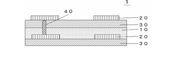
- FIG. 1 is a schematic diagram showing an example of a cross section of a multilayer wiring board.
- FIG. 1 is an example of a cross section of a two-layer wiring board.
- a multilayer wiring board 1 shown in FIG. 1 includes a fluororesin substrate 30 having a conductor pattern 20 formed on at least one surface thereof, and an adhesive layer 10 for bonding the fluororesin substrate 30.
- the adhesive layer 10 contains a cured product of a thermosetting resin. Furthermore, the elongation at break of the adhesive layer 10 is 20% or more and 300% or less.
- via holes (through holes) 40 can be formed in the multilayer wiring board 1 as necessary.
- fluororesin substrate for example, a fluororesin substrate described in JP-A-07-323501 or JP-A-2005-268365 can be used.
- PTFE polytetrafluoroethylene
- fluororesin used for fluororesin substrates examples include polytetrafluoroethylene (PTFE), tetrafluoroethylene / perfluoroalkyl vinyl ether copolymer (PFA), tetrafluoroethylene / hexafluoropropylene / perfluoroalkyl vinyl ether copolymer (FEPPFA), FEP, polychlorotrifluoroethylene (PCTFE), vinylidene fluoride resin (PVDF), vinyl fluoride resin (PVF), ethylene-tetrafluoroethylene copolymer (ETFE), and ethylene-chlorotrifluoro An ethylene copolymer (ECTFE) is mentioned.
- PTFE polytetrafluoroethylene
- PFA perfluoroalkyl vinyl ether copolymer
- FEPPFA tetrafluoroethylene / hexafluoropropylene / perfluoroalkyl vinyl ether copolymer
- FEP
- PTFE is preferable from the viewpoints of low dielectric constant, low dielectric loss tangent, heat resistance, chemical resistance, and the like.
- the melting point of PFA or the like is preferably 280 ° C. or higher.
- An example of the molding temperature of the fluororesin is 320 to 400 ° C.
- the fluororesin may be used alone or in combination of two or more.
- heat resistant insulating fibers examples include inorganic fibers such as glass fibers, silica fibers, alumina fibers, and aluminum silicate fibers, polyparaphenylene benzobisoxazole fibers (PBO fibers), aromatic polyester fibers, polyphenylene sulfide fibers, and Organic fibers such as wholly aromatic polyamide fibers can be mentioned.
- Glass fiber is preferable from the viewpoints of heat resistance, high strength, high elastic modulus, and low cost.
- the heat resistant insulating fibers may be used alone or in combination of two or more.
- Examples of the conductor pattern include copper wiring formed by etching copper foil.
- the adhesive layer contains a cured product of a thermosetting resin, and the elongation at break of the adhesive layer is 20% or more and 300% or less.
- the thermosetting resin imparts adhesion and heat resistance (melting resistance during heating) to the adhesive layer.
- the thermosetting resin is not particularly limited as long as it gives the adhesive layer a breaking elongation of 20% or more and 300% or less after the thermosetting.
- examples include modified polyphenylene ether, bisphenol A type epoxy resin, biphenyl type epoxy resin, naphthalene type epoxy resin, bismaleimide, special acrylate, and modified polyimide.
- a resin containing modified polyphenylene ether or modified polyimide is preferable from the viewpoint of the elongation at break and dielectric constant of the adhesive layer.
- a modified polyphenylene ether having an ethylenically unsaturated group (particularly, a styrene group) at the terminal is high in both low-polarity fluororesins because of its small polarity. Since it has adhesiveness, it is more preferable.
- an epoxy resin alone is not preferable because it has a low elongation at break and a high dielectric constant.
- the thermosetting resins may be used alone or in combination of two or more.
- An epoxy resin as a thermosetting resin may require a curing agent.
- the curing agent is not particularly limited. Examples include imidazole, amine, acid anhydride, and phenolic curing agents. From the viewpoint of reaction temperature and reaction time, an imidazole-based curing agent is preferable. 1-benzyl-2-phenylimidazole and 2-phenyl-4,5-dihydroxymethylimidazole are more preferred.
- Other resin can be contained in the adhesive layer.
- the other resin is added to improve the elongation when the thermosetting resin alone cannot give a breaking elongation of 20% or more to the adhesive layer after thermosetting.
- examples of other resins include polyolefin-based elastomers, especially styrene-based thermoplastic elastomers, polystyrene-poly (ethylene / butylene) block copolymers, polystyrene-poly (ethylene-ethylene / propylene) block copolymers. Etc. are mentioned. These hydrogenated elastomers are preferred because of their low dielectric constant and dielectric loss tangent.
- Other resins may be used alone or in combination of two or more.
- the elongation at break of the adhesive layer is preferably 20% or more and 300% or less from the viewpoint of peel strength with the copper foil.
- the elongation at break is less than 20%, the adhesive layer becomes hard and brittle. Therefore, the peel strength with the copper foil is weakened. If the elongation at break exceeds 300%, misalignment tends to occur during lamination.
- the elongation at break of the adhesive layer can be measured by an autograph.
- the adhesive layer preferably contains a filler having a dielectric loss tangent of 0.002 or less from the viewpoint of further reducing transmission loss of the multilayer wiring board.
- fillers having a dielectric loss tangent of 0.002 or less include fluororesin fillers and silica fillers (including hollow silica particles).
- the average particle size of the filler having a dielectric loss tangent of 0.002 or less is preferably 0.01 to 10 ⁇ m, more preferably 0.01 to 1 ⁇ m.
- the average particle diameter can be measured with a laser diffraction particle size distribution measuring apparatus (model number: LS13320) manufactured by BECKMAN COULTER.
- the filler having a dielectric loss tangent of 0.002 or less may be used alone or in combination of two or more.
- an additive can be further blended as necessary within a range that does not impair the purpose of the present embodiment.
- additives include leveling agents, antifoaming agents, thixotropic agents, antioxidants, pigments, or dyes.
- the tensile elastic modulus of the adhesive layer is preferably 1 GPa or less from the viewpoint of relaxation of internal stress of the multilayer wiring board as a laminate and peel strength between the fluororesin and the adhesive layer.
- the tensile elastic modulus of the adhesive layer is preferably 0.1 GPa or more from the viewpoint of pressure resistance during pressing. When the elastic modulus is less than 0.1 GPa, the heat resistance of the adhesive layer (such as during hot pressing) is inferior, and misalignment tends to occur.
- the dielectric constant of the adhesive layer is preferably 70 to 130%.
- the dielectric constant of the adhesive layer in this range approximates the dielectric constant of the fluororesin substrate. This simplifies the design of the multilayer wiring board.
- the transmission loss on the adhesive layer is preferably 0 to ⁇ 3 dB / 70 mm at 20 GHz from the viewpoint of efficient transmission and reception of electric signals.
- the adhesive layer can be laminated at a low temperature of 200 ° C. or less, preferably from the viewpoint of low power (low energy) and reduction of thermal damage to the member.
- the multilayer wiring board of the present disclosure includes a fluororesin substrate having a conductor pattern formed on at least one surface thereof, and an adhesive layer for bonding the fluororesin substrate.
- the adhesive layer contains a cured product of a thermosetting resin and has an elongation at break of 20% to 300%.
- This multilayer wiring board is excellent in the peel strength between the fluororesin substrate and the adhesive layer and the peel strength between the conductor pattern and the adhesive layer. The reason for this excellent peel strength is considered to be the anchoring effect. It is considered that the elongation at break of the adhesive layer contributes to the peel strength with the conductor (copper foil).
- the copper foil peel strength becomes weak.
- peel strength between the fluororesin substrate and the adhesive layer is high, peeling may occur between the fluororesin substrate and the copper foil in the peel test, or the fluororesin substrate itself may be destroyed.
- a semiconductor device of the present disclosure includes the multilayer wiring board described above.
- Examples of the semiconductor device include a millimeter wave antenna and a radio base station.
- thermosetting resin 1 modified polyphenylene ether (product name: OPE2St2200) manufactured by Mitsubishi Gas Chemical was used.
- thermosetting resin 2 modified polyphenylene ether (product name: OPE2St1200) manufactured by Mitsubishi Gas Chemical was used.
- thermosetting resin 3 a bisphenol A type epoxy resin (product name: LX-01) manufactured by Osaka Soda was used.
- thermosetting resin 4 Nippon Kayaku biphenyl type epoxy resin (product name: NC3000) was used.
- thermosetting resin 5 DIC naphthalene type epoxy resin (product name: HP4032D) was used.
- thermosetting resin 6 bis- (3-ethyl-5-methyl-4-maleimidophenyl) methane (product name: BMI-70), which is bismaleimide made by Kay Chemical Co., Ltd., was used.
- thermosetting resin 7 N-acryloyloxyethyl hexahydrophthalimide (product name: M-140), a special acrylate manufactured by Toagosei Co., Ltd., was used.
- imidazole product name: 1B2PZ
- Shikoku Kasei Imidazole product name: 2PHZ
- Kraton polymer elastomer SEBS (product name: G1652) was used.
- Kraton polymer elastomer SEBS (product name: G1657) was used.
- Kuraray elastomer SEEPS (product name: Septon 4044) was used.
- an elastomer SEBS (product name: Tuftec H1052) manufactured by Asahi Kasei Chemicals Corporation was used.
- JSR elastomer SBS product name: TR2003
- the filler a fluororesin filler manufactured by Daikin Industries (product name: Lubron L-2, average particle size: 2 ⁇ m) was used.
- Admatex silica filler product name: SE2050, average particle size: 0.5 ⁇ m
- the dielectric loss tangent of filler 1 and the dielectric loss tangent of filler 2 were both 0.002 or less.
- Examples 1 to 4 Comparative Examples 1 to 4
- each component was metered. Thereafter, these components were put into a reaction kettle heated to 80 ° C., and atmospheric pressure dissolution and mixing were performed for 3 hours while rotating at a rotation speed of 250 rpm. However, the curing agent was added after cooling. Although not shown in Table 1, toluene was used for dissolution and viscosity adjustment.
- the varnish containing the composition for the adhesive layer thus obtained was applied to one surface of a support (PET film subjected to a release treatment).
- the varnish was dried at 100 ° C. to obtain a film for an adhesive layer with a support (thickness of the adhesive layer: about 25 ⁇ m and about 50 ⁇ m).
- the film for an adhesive layer with a support was subjected to vacuum hot press curing at 200 ° C., 60 min, and 1 MPa.
- the adhesive layer film with a support after curing was cut into 15 mm ⁇ 150 mm. After peeling off the support, in the longitudinal direction, it was pulled with an autograph at a pulling speed of 200 mm / min, and the length that was stretched to break was measured.
- the elongation at break of the adhesive layer is a value obtained by dividing the length at break by the initial length and expressed as a percentage. Table 1 shows the measurement results of the elongation at break of the adhesive layer.
- the tensile elastic modulus of the adhesive layer is preferably 0.1 to 1 GPa or less. Table 1 shows the measurement results of the tensile elastic modulus of the adhesive layer.
- Fluororesin substrate (product name: CGS-500) manufactured by Chukoh Kasei Kogyo Co., Ltd. on one side of the adhesive layer film peeled off from the support, and copper foil (thickness) manufactured by Fukuda Metal Foil Powder Co., Ltd. on the other side
- the thickness was 35 ⁇ m and the product name was CF-T8G-HTE), which were bonded together under vacuum hot pressing at 200 ° C., 60 min, and 2 MPa. In this way, a laminated member was produced.
- the copper foil or the fluororesin substrate was peeled off by an autograph, and the peel strength (90 ° peel) was measured.
- the peel strength is preferably 7 N / cm or more. Table 1 shows the measurement results of peel strength.
- the adhesive layer film with the support was vacuum hot press cured under the conditions of 200 ° C., 60 min, and 1 MPa.
- a cured film with a support 70 mm ⁇ 130 mm was cut out from the adhesive layer film with a support after curing.
- the thickness of the test piece was measured.
- the dielectric constant ( ⁇ ) and dielectric loss tangent (tan ⁇ ) of the test piece were measured by the SPDR method (1.9 GHz).
- the dielectric constant is preferably 1.6 to 3.5, more preferably 2.0 to 2.9.
- the dielectric loss tangent is preferably 0.0005 to 0.005.
- the ratio (unit:%) of the dielectric constant of the adhesive layer when the dielectric constant of the fluororesin substrate was 100% was calculated.
- the dielectric constant of the used fluororesin substrate was 2.24.
- the dielectric constant of the adhesive layer is preferably 70 to 130%.
- the produced substrate was measured at 20 GHz using a network analyzer (manufactured by Keysight, N5245A).
- the measured value of the obtained S parameter insertion loss (S21) was defined as the transmission loss on the adhesive layer.
- the transmission loss on the adhesive layer is preferably 0 to ⁇ 3 dB / 70 mm at 20 GHz.
- the transmission loss of the adhesive layer was -2.2 dB in Example 1, -2.7 dB in Example 2, -2.1 dB in Example 3, and -2.3 dB in Example 4.
- Comparative Examples 1 and 4 in which the elongation at break of the adhesive layer was too low, the peel strength with the copper foil was low.
- Comparative Example 2 where the elongation at break of the adhesive layer was too high, the peel strength with the fluororesin substrate and the peel strength with the copper foil were both low.
- Comparative Example 3 in which the elongation at break of the adhesive layer was too high, the peel strength with the copper foil was low.
- the transmission loss of the adhesive layer of Comparative Example 1 was ⁇ 3.6 dB.
- the multilayer wiring board of the present disclosure uses a thermosetting resin that suppresses misalignment between layers, and uses an adhesive layer that has excellent peel strength. The transmission loss of electrical signals is low. Therefore, the multilayer wiring board of the present disclosure is very useful.
Landscapes
- Chemical & Material Sciences (AREA)
- Organic Chemistry (AREA)
- Engineering & Computer Science (AREA)
- Microelectronics & Electronic Packaging (AREA)
- Manufacturing & Machinery (AREA)
- Inorganic Chemistry (AREA)
- Laminated Bodies (AREA)
- Production Of Multi-Layered Print Wiring Board (AREA)
- Adhesives Or Adhesive Processes (AREA)
- Adhesive Tapes (AREA)
Abstract
Description
〔1〕少なくともその一面に形成されている導体パターンを有するフッ素樹脂基板と、前記フッ素樹脂基板を接着するための接着層と、を含み、前記接着層が熱硬化性樹脂の硬化物を含有し、かつ、20%以上300%以下の破断伸び率を有する、多層配線基板。
〔2〕前記接着層の引張り弾性率が、1GPa以下である、上記〔1〕の多層配線基板。
〔3〕前記接着層が、0.002以下の誘電正接を有するフィラーを含む、上記〔1〕または〔2〕の多層配線基板。
〔4〕前記フッ素樹脂基板の誘電率が100%であるときの、前記接着層の誘電率が、70~130%である、上記〔1〕~〔3〕のいずれかの多層配線基板。
〔5〕前記接着層上の伝送損失が、20GHzにおいて、0~-3dB/70mmである、上記〔1〕~〔4〕のいずれかの多層配線基板。
〔6〕上記〔1〕~〔5〕のいずれかの多層配線基板を含む、半導体装置。
なお、図1に示すように、多層配線基板1には、必要に応じ、ヴィアホール(スルーホール)40を形成することができる。
フッ素樹脂基板としては、例えば、特開平07-323501号公報あるいは特開2005-268365号公報に記載のフッ素樹脂基板を使用できる。具体的な例として、ガラスクロスに、ポリテトラフルオロエチレン(PTFE)を含浸保持させて得られる、プリプレグから構成したリジッド基板、および、フッ素樹脂繊維と、ガラス繊維などの耐熱性絶縁繊維と、を用いて、湿式抄紙法にて形成することにより得られる、いわゆる抄紙シートが、挙げられる。
接着層は、熱硬化性樹脂の硬化物を含有し、かつ、この接着層の破断伸び率は、20%以上300%以下である。
上述のとおり、本開示の多層配線基板は、少なくともその一面に形成されている導体パターンを有するフッ素樹脂基板と、そのフッ素樹脂基板を接着するための接着層と、を含む。その接着層は、熱硬化性樹脂の硬化物を含有し、かつ、20%以上300%以下の破断伸び率を有する。この多層配線基板は、フッ素樹脂基板と接着層との間のピール強度、および導体パターンと接着層との間のピ-ル強度に優れる。この優れたピ-ル強度の原因は、投錨効果(アンカー効果)による、と考えられる。接着層の破断伸び率が、導体(銅箔)とのピール強度に寄与することが考えられる。破断伸び率が20%未満または300%を超えると、銅箔ピール強度は弱くなる。なお、フッ素樹脂基板と接着層と間のピール強度が高いため、ピール試験では、フッ素樹脂基板と銅箔との間で剥離が生じたり、フッ素樹脂基板自体が破壊される場合がある。
本開示の半導体装置は、上述の多層配線基板を含む。半導体装置の例としては、ミリ波アンテナおよび無線基地局が、挙げられる。
熱硬化性樹脂2として、三菱ガス化学製変性ポリフェニレンエーテル(品名:OPE2St1200)が、使用された。
熱硬化性樹脂3として、大阪ソーダ製ビスフェノールA型エポキシ樹脂(品名:LX-01)が、使用された。
熱硬化性樹脂4として、日本化薬製ビフェニル型エポキシ樹脂(品名:NC3000)が、使用された。
熱硬化性樹脂5として、DIC製ナフタレン型エポキシ樹脂(品名:HP4032D)が、使用された。
熱硬化性樹脂6として、ケイ・アイ化成製ビスマレイミドである、ビス-(3-エチル-5-メチル-4-マレイミドフェニル)メタン(品名:BMI-70)が、使用された。
熱硬化性樹脂7として、東亞合成製特殊アクリレートである、N-アクリロイルオキシエチルヘキサヒドロフタルイミド(品名:M-140)が、使用された。
硬化剤1として、四国化成製イミダゾール(品名:1B2PZ)が、使用された。
硬化剤2として、四国化成製イミダゾール(品名:2PHZ)が、使用された。
その他の樹脂1として、クレイトンポリマー製エラストマーSEBS(品名:G1652)が、使用された。
その他の樹脂2として、クレイトンポリマー製エラストマーSEBS(品名:G1657)が、使用された。
その他の樹脂3として、クラレ製エラストマーSEEPS(品名:セプトン4044)が、使用された。
その他の樹脂4として、旭化成ケミカルズ製エラストマーSEBS(品名:タフテックH1052)が、使用された。
その他の樹脂5として、JSR製エラストマーSBS(品名:TR2003)が、使用された。
フィラー1として、ダイキン工業製フッ素樹脂フィラー(品名:ルブロン L-2、平均粒径:2μm)が、使用された。
フィラー2として、アドマテックス シリカフィラー(品名:SE2050、平均粒径:0.5μm)が、使用された。
なお、フィラー1の誘電正接、および、フィラー2の誘電正接は、いずれも0.002以下であった。
表1に示す配合で、各成分が計量配合された。その後、それら成分を80℃に加温された反応釜に投入して、回転数250rpmで回転させながら、常圧溶解混合を3時間行った。ただし、硬化剤は、冷却後に加えた。なお、表1には記載していないが、溶解および粘度調整にトルエンを使用した。
支持体付の接着層用フィルムを、200℃、60min、および1MPaの条件で真空熱プレス硬化させた。硬化後の支持体付の接着層用フィルムを、15mm×150mmに切り出した。支持体を剥がした後、長手方向に、引張り速度200mm/minで、オートグラフで引張り、破断までに伸びた長さを測定した。接着層の破断伸び率は、破断時の長さを、初期の長さで除して得られる値を、パーセントで表示した値である。表1に、接着層の破断伸び率の測定結果を示す。
支持体付の接着層用フィルムを、200℃、60min、および1MPaの条件で、真空熱プレス硬化させた。硬化後の支持体付の接着層用フィルムから、25mm×250mmの支持体付の硬化フィルムを切り出した。支持体付の硬化フィルムから支持体を剥がして試験片を得た後、試験片の厚みを測定した。次いで、オートグラフを用いて、試験片を、その長手方向に、引張速度1mm/minで、引っ張った。そして、1~2mmまでに試験片が伸びた時の、応力ひずみ曲線の傾きを測定した。この値を断面積で除して、接着層の引張り弾性率を求めた。接着層の引張り弾性率は、好ましくは0.1~1GPa以下である。表1に、接着層の引張り弾性率の測定結果を示す。
支持体からはがした接着層用フィルムの一面に、中興化成工業(株)製フッ素樹脂基板(品名:CGS-500)を、他の一面に福田金属箔粉工業(株)製銅箔(厚さ:35μm、品名:CF-T8G-HTE)を、200℃、60min、および2MPaの条件で、真空熱プレスしながら、貼りあわせた。このようにして、積層部材を作製した。その後、JIS K6854-1に準拠して、銅箔またはフッ素樹脂基板をオートグラフで引きはがして、ピール強度(90°ピール)を測定した。ピール強度は、好ましくは7N/cm以上である。表1に、ピール強度の測定結果を示す。
上記と同じ方法で作製した積層部材を、260℃のはんだ浴に1分間浮かべて、剥離および膨れの有無を、目視で確認した。
支持体付の接着層用フィルムを、200℃、60min、1MPaの条件で、真空熱プレス硬化させた。硬化後の支持体付の接着層用フィルムから、支持体付の硬化フィルム(70mm×130mm)を切り出した。支持体付の硬化フィルムから支持体を剥離して試験片を得た後、試験片の厚みを測定した。次いで、SPDR法(1.9GHz)により、試験片の誘電率(ε)および誘電正接(tanδ)を測定した。誘電率は、好ましくは1.6~3.5、より好ましくは2.0~2.9である。誘電正接は、好ましくは0.0005~0.005である。
次に、フッ素樹脂基板の誘電率が100%であるときの、接着層の誘電率の比(単位:%)を計算した。使用したフッ素樹脂基板の誘電率は、2.24であった。フッ素樹脂基板の誘電率が100%であるとき、接着層の誘電率は、好ましくは70~130%である。
支持体を取り除いた後の、厚み50μmの熱硬化前の接着層用フィルムを、2枚の銅箔(福田金属箔粉(株)製、18μm、CF-T9FZ-SV)間に挟み、次いで、200℃、60min、1MPaの条件で、真空熱プレスした。このようにして、銅張基板を作製した。この銅張基板の一面に、インピーダンス50Ωとなるように、エッチング処理により、信号配線長70mmとなる信号配線とグランドパッドを作製した。銅張基板の他の一面は、グランド層とした。グランドパッドとグランド層との接続をとるため、スルーホールを作製したのち、銅めっき処理を行った。これにより、50Ωのマイクロストリップライン基板を作製した。この時、銅めっき処理により配線高さは約30μmとなった。作製した基板を、ネットワークアナライザー(キーサイト製、N5245A)を用いて、20GHzで測定した。得られたSパラメーター挿入損失(S21)の測定値を接着層上の伝送損失と定義した。接着層上の伝送損失は、20GHzにおいて、好ましくは0~-3dB/70mmである。

10 接着層
20 導体パターン
30 フッ素樹脂基板
40 ヴィアホール(スルーホール)
Claims (6)
- 少なくともその一面に形成されている導体パターンを有するフッ素樹脂基板と、
前記フッ素樹脂基板を接着するための接着層と、
を含み、
前記接着層が、熱硬化性樹脂の硬化物を含有し、かつ、20%以上300%以下の破断伸び率を有する、多層配線基板。 - 前記接着層の引張り弾性率が、1GPa以下である、請求項1記載の多層配線基板。
- 前記接着層が、0.002以下の誘電正接を有するフィラーを含む、請求項1または2記載の多層配線基板。
- 前記フッ素樹脂基板の誘電率が100%であるときの、前記接着層の誘電率が、70~130%である、請求項1~3のいずれか1項に記載の多層配線基板。
- 前記接着層上の伝送損失が、20GHzにおいて、0~-3dB/70mmである、請求項1~4のいずれか1項に記載の多層配線基板。
- 請求項1~5のいずれか1項に記載の多層配線基板を含む、半導体装置。
Priority Applications (8)
| Application Number | Priority Date | Filing Date | Title |
|---|---|---|---|
| US16/487,929 US20200058577A1 (en) | 2017-02-22 | 2018-02-20 | Multi-layer wiring substrate and semiconductor device |
| KR1020227041841A KR102566108B1 (ko) | 2017-02-22 | 2018-02-20 | 접착층용 필름, 다층 배선 기판, 및 반도체 장치 |
| KR1020197023434A KR102473321B1 (ko) | 2017-02-22 | 2018-02-20 | 다층 배선 기판 및 반도체 장치 |
| EP18756912.4A EP3589093A4 (en) | 2017-02-22 | 2018-02-20 | MULTI-LAYER WIRING SUBSTRATE AND SEMICONDUCTOR DEVICE |
| JP2019501329A JP7148146B2 (ja) | 2017-02-22 | 2018-02-20 | 多層配線基板および半導体装置 |
| CN201880010156.4A CN110249715B (zh) | 2017-02-22 | 2018-02-20 | 多层布线基板及半导体装置 |
| JP2022069235A JP7313736B2 (ja) | 2017-02-22 | 2022-04-20 | 接着層用フィルム、多層配線基板および半導体装置 |
| JP2023110420A JP2023126302A (ja) | 2017-02-22 | 2023-07-05 | 多層配線基板および半導体装置 |
Applications Claiming Priority (2)
| Application Number | Priority Date | Filing Date | Title |
|---|---|---|---|
| JP2017031408 | 2017-02-22 | ||
| JP2017-031408 | 2017-02-22 |
Publications (1)
| Publication Number | Publication Date |
|---|---|
| WO2018155418A1 true WO2018155418A1 (ja) | 2018-08-30 |
Family
ID=63253893
Family Applications (1)
| Application Number | Title | Priority Date | Filing Date |
|---|---|---|---|
| PCT/JP2018/005932 Ceased WO2018155418A1 (ja) | 2017-02-22 | 2018-02-20 | 多層配線基板および半導体装置 |
Country Status (7)
| Country | Link |
|---|---|
| US (1) | US20200058577A1 (ja) |
| EP (1) | EP3589093A4 (ja) |
| JP (3) | JP7148146B2 (ja) |
| KR (2) | KR102473321B1 (ja) |
| CN (1) | CN110249715B (ja) |
| TW (1) | TWI818904B (ja) |
| WO (1) | WO2018155418A1 (ja) |
Cited By (7)
| Publication number | Priority date | Publication date | Assignee | Title |
|---|---|---|---|---|
| JP2021070592A (ja) * | 2019-10-29 | 2021-05-06 | 日鉄ケミカル&マテリアル株式会社 | シリカ粒子、樹脂組成物、樹脂フィルム及び金属張積層板 |
| JP2021070160A (ja) * | 2019-10-29 | 2021-05-06 | 昭和電工マテリアルズ株式会社 | フッ素樹脂基板積層体 |
| JP2022050927A (ja) * | 2020-09-18 | 2022-03-31 | 住友ベークライト株式会社 | 金属箔付樹脂フィルムおよび高周波回路用基板の製造方法 |
| JPWO2022210673A1 (ja) * | 2021-03-30 | 2022-10-06 | ||
| JP2022170140A (ja) * | 2021-04-28 | 2022-11-10 | 昭和電工マテリアルズ株式会社 | フッ素樹脂基板積層体及びフッ素樹脂基板積層体の製造方法 |
| WO2024204006A1 (ja) * | 2023-03-30 | 2024-10-03 | 住友電工プリントサーキット株式会社 | プリント配線板 |
| WO2024253037A1 (ja) * | 2023-06-08 | 2024-12-12 | Agc株式会社 | 樹脂付金属箔 |
Families Citing this family (4)
| Publication number | Priority date | Publication date | Assignee | Title |
|---|---|---|---|---|
| US12624261B2 (en) | 2020-03-31 | 2026-05-12 | Lintec Corporation | Adhesive for high-frequency dielectric heating, structure, and manufacturing method of structure |
| JP7478031B2 (ja) | 2020-06-02 | 2024-05-02 | 信越化学工業株式会社 | 低誘電シリカ粉体の製造方法 |
| US20230299461A1 (en) * | 2020-07-03 | 2023-09-21 | Namics Corporation | Antenna-equipped semiconductor package and resin composition for antenna-equipped semiconductor package |
| JP2025096895A (ja) * | 2023-12-18 | 2025-06-30 | artience株式会社 | プリント配線板用接着シート、金属張積層板、プリント配線板、および電子機器 |
Citations (9)
| Publication number | Priority date | Publication date | Assignee | Title |
|---|---|---|---|---|
| JPH07323501A (ja) | 1994-06-01 | 1995-12-12 | Nippon Pillar Packing Co Ltd | 多層板用プリプレグ、積層板、多層プリント回路基板およびその製造方法 |
| JP2004059644A (ja) | 2002-07-25 | 2004-02-26 | Mitsubishi Gas Chem Co Inc | ビニル化合物およびその硬化物 |
| JP2005268365A (ja) | 2004-03-17 | 2005-09-29 | Nippon Pillar Packing Co Ltd | 多層プリント回路基板とその製造方法 |
| JP2006059865A (ja) * | 2004-08-17 | 2006-03-02 | Unitika Ltd | 基板及びその製造方法 |
| JP2007098692A (ja) | 2005-09-30 | 2007-04-19 | Nippon Pillar Packing Co Ltd | 銅張積層板、プリント配線板及び多層プリント配線板並びにこれらの製造方法 |
| JP2008056820A (ja) * | 2006-08-31 | 2008-03-13 | Toagosei Co Ltd | ハロゲンフリー難燃性接着剤組成物 |
| JP2011011456A (ja) * | 2009-07-02 | 2011-01-20 | Toyobo Co Ltd | 多層フッ素樹脂フィルムおよび多層フッ素樹脂基板 |
| JP2012243923A (ja) * | 2011-05-19 | 2012-12-10 | Fujikura Ltd | フレキシブルプリント回路及びその製造方法 |
| JP2016124982A (ja) * | 2014-12-27 | 2016-07-11 | 新日鉄住金化学株式会社 | 架橋ポリイミド樹脂、その製造方法、接着剤樹脂組成物、その硬化物、カバーレイフィルム及び回路基板 |
Family Cites Families (15)
| Publication number | Priority date | Publication date | Assignee | Title |
|---|---|---|---|---|
| JP2001203466A (ja) * | 2000-01-20 | 2001-07-27 | Nippon Shokubai Co Ltd | 多層プリント基板 |
| JP2003133814A (ja) * | 2001-10-24 | 2003-05-09 | Kyocera Corp | 高周波用配線基板 |
| JP2003298196A (ja) * | 2002-04-03 | 2003-10-17 | Japan Gore Tex Inc | プリント配線板用誘電体フィルム、多層プリント基板および半導体装置 |
| JP4325337B2 (ja) * | 2003-09-19 | 2009-09-02 | 日立化成工業株式会社 | 樹脂組成物、それを用いたプリプレグ、積層板及び多層プリント配線板 |
| JP2005174161A (ja) * | 2003-12-15 | 2005-06-30 | Konica Minolta Photo Imaging Inc | Icカード及びicカードの製造方法 |
| JP2006024618A (ja) * | 2004-07-06 | 2006-01-26 | Toshiba Corp | 配線基板 |
| TWI404744B (zh) * | 2006-08-08 | 2013-08-11 | Namics Corp | 熱硬化性樹脂組成物及由該樹脂組成物構成之未硬化膜片 |
| GB201102672D0 (en) * | 2011-02-15 | 2011-03-30 | Zephyros Inc | Improved structural adhesives |
| JP6034019B2 (ja) * | 2011-12-21 | 2016-11-30 | リンテック株式会社 | 保護膜形成層付ダイシングシートおよびチップの製造方法 |
| JP2014207297A (ja) * | 2013-04-11 | 2014-10-30 | 株式会社フジクラ | フレキシブルプリント回路及びその製造方法 |
| US10383215B2 (en) * | 2013-05-31 | 2019-08-13 | Sumitomo Electric Industries, Ltd. | Radio-frequency printed circuit board and wiring material |
| WO2015053309A1 (ja) * | 2013-10-11 | 2015-04-16 | 住友電工プリントサーキット株式会社 | フッ素樹脂基材、プリント配線板、及び回路モジュール |
| CN106415819A (zh) * | 2014-01-22 | 2017-02-15 | 琳得科株式会社 | 保护膜形成膜、保护膜形成用片、保护膜形成用复合片及检查方法 |
| CN107207932B (zh) * | 2015-01-19 | 2019-10-25 | 株式会社巴川制纸所 | 热固化性粘合剂组合物、热固化性粘合膜以及复合膜 |
| HK1244833B (zh) * | 2015-03-23 | 2019-11-29 | 拓自达电线株式会社 | 树脂浸渗物、复合材料和覆铜层叠体的制造方法 |
-
2018
- 2018-02-20 US US16/487,929 patent/US20200058577A1/en not_active Abandoned
- 2018-02-20 WO PCT/JP2018/005932 patent/WO2018155418A1/ja not_active Ceased
- 2018-02-20 JP JP2019501329A patent/JP7148146B2/ja active Active
- 2018-02-20 KR KR1020197023434A patent/KR102473321B1/ko active Active
- 2018-02-20 EP EP18756912.4A patent/EP3589093A4/en active Pending
- 2018-02-20 CN CN201880010156.4A patent/CN110249715B/zh active Active
- 2018-02-20 KR KR1020227041841A patent/KR102566108B1/ko active Active
- 2018-02-22 TW TW107105908A patent/TWI818904B/zh active
-
2022
- 2022-04-20 JP JP2022069235A patent/JP7313736B2/ja active Active
-
2023
- 2023-07-05 JP JP2023110420A patent/JP2023126302A/ja not_active Withdrawn
Patent Citations (9)
| Publication number | Priority date | Publication date | Assignee | Title |
|---|---|---|---|---|
| JPH07323501A (ja) | 1994-06-01 | 1995-12-12 | Nippon Pillar Packing Co Ltd | 多層板用プリプレグ、積層板、多層プリント回路基板およびその製造方法 |
| JP2004059644A (ja) | 2002-07-25 | 2004-02-26 | Mitsubishi Gas Chem Co Inc | ビニル化合物およびその硬化物 |
| JP2005268365A (ja) | 2004-03-17 | 2005-09-29 | Nippon Pillar Packing Co Ltd | 多層プリント回路基板とその製造方法 |
| JP2006059865A (ja) * | 2004-08-17 | 2006-03-02 | Unitika Ltd | 基板及びその製造方法 |
| JP2007098692A (ja) | 2005-09-30 | 2007-04-19 | Nippon Pillar Packing Co Ltd | 銅張積層板、プリント配線板及び多層プリント配線板並びにこれらの製造方法 |
| JP2008056820A (ja) * | 2006-08-31 | 2008-03-13 | Toagosei Co Ltd | ハロゲンフリー難燃性接着剤組成物 |
| JP2011011456A (ja) * | 2009-07-02 | 2011-01-20 | Toyobo Co Ltd | 多層フッ素樹脂フィルムおよび多層フッ素樹脂基板 |
| JP2012243923A (ja) * | 2011-05-19 | 2012-12-10 | Fujikura Ltd | フレキシブルプリント回路及びその製造方法 |
| JP2016124982A (ja) * | 2014-12-27 | 2016-07-11 | 新日鉄住金化学株式会社 | 架橋ポリイミド樹脂、その製造方法、接着剤樹脂組成物、その硬化物、カバーレイフィルム及び回路基板 |
Cited By (10)
| Publication number | Priority date | Publication date | Assignee | Title |
|---|---|---|---|---|
| JP2021070592A (ja) * | 2019-10-29 | 2021-05-06 | 日鉄ケミカル&マテリアル株式会社 | シリカ粒子、樹脂組成物、樹脂フィルム及び金属張積層板 |
| JP2021070160A (ja) * | 2019-10-29 | 2021-05-06 | 昭和電工マテリアルズ株式会社 | フッ素樹脂基板積層体 |
| JP7529392B2 (ja) | 2019-10-29 | 2024-08-06 | 日鉄ケミカル&マテリアル株式会社 | シリカ粒子、樹脂組成物、樹脂フィルム及び金属張積層板 |
| JP7824027B2 (ja) | 2019-10-29 | 2026-03-04 | 株式会社レゾナック | フッ素樹脂基板積層体 |
| JP2022050927A (ja) * | 2020-09-18 | 2022-03-31 | 住友ベークライト株式会社 | 金属箔付樹脂フィルムおよび高周波回路用基板の製造方法 |
| JPWO2022210673A1 (ja) * | 2021-03-30 | 2022-10-06 | ||
| JP2022170140A (ja) * | 2021-04-28 | 2022-11-10 | 昭和電工マテリアルズ株式会社 | フッ素樹脂基板積層体及びフッ素樹脂基板積層体の製造方法 |
| JP7786044B2 (ja) | 2021-04-28 | 2025-12-16 | 株式会社レゾナック | フッ素樹脂基板積層体及びフッ素樹脂基板積層体の製造方法 |
| WO2024204006A1 (ja) * | 2023-03-30 | 2024-10-03 | 住友電工プリントサーキット株式会社 | プリント配線板 |
| WO2024253037A1 (ja) * | 2023-06-08 | 2024-12-12 | Agc株式会社 | 樹脂付金属箔 |
Also Published As
| Publication number | Publication date |
|---|---|
| KR20190121298A (ko) | 2019-10-25 |
| CN110249715B (zh) | 2022-08-23 |
| US20200058577A1 (en) | 2020-02-20 |
| JP2023126302A (ja) | 2023-09-07 |
| JP2022115868A (ja) | 2022-08-09 |
| CN110249715A (zh) | 2019-09-17 |
| TW201843047A (zh) | 2018-12-16 |
| JPWO2018155418A1 (ja) | 2019-12-12 |
| EP3589093A4 (en) | 2020-12-23 |
| JP7313736B2 (ja) | 2023-07-25 |
| JP7148146B2 (ja) | 2022-10-05 |
| KR102566108B1 (ko) | 2023-08-11 |
| KR102473321B1 (ko) | 2022-12-01 |
| TWI818904B (zh) | 2023-10-21 |
| KR20220164623A (ko) | 2022-12-13 |
| EP3589093A1 (en) | 2020-01-01 |
Similar Documents
| Publication | Publication Date | Title |
|---|---|---|
| JP7313736B2 (ja) | 接着層用フィルム、多層配線基板および半導体装置 | |
| JP6572983B2 (ja) | エポキシ樹脂組成物 | |
| TWI679257B (zh) | 樹脂組合物、接著膜、覆蓋膜、積層板、附有樹脂之銅箔及附有樹脂之銅箔積層板 | |
| CN103650649B (zh) | 粘接膜、使用了该粘接膜的多层印制电路板、及该多层印制电路板的制造方法 | |
| KR101413203B1 (ko) | 회로 기판 제조용 시아네이트 에스테르계 수지 조성물 | |
| TWI677528B (zh) | 多層印刷配線板之絕緣層用的熱硬化性環氧樹脂組成物、多層印刷配線板之絕緣層用的接著薄膜及多層印刷配線板 | |
| CN101652401A (zh) | 环氧树脂组合物、预浸料坯、层叠板、多层印刷线路板、半导体器件、绝缘树脂片、和制造多层印刷线路板的方法 | |
| KR20090101968A (ko) | 캐리어 장착 프리프레그의 제조방법, 캐리어 장착 프리프레그, 박형 양면판의 제조방법, 박형 양면판, 및 다층 프린트 배선판의 제조방법 | |
| KR101511495B1 (ko) | 에폭시 수지 조성물 | |
| TWI808062B (zh) | 層間絕緣膜及其製造方法 | |
| WO2014192322A1 (ja) | 高周波用プリント配線板及び配線材料 | |
| TWI837306B (zh) | 樹脂組成物、預浸體、附樹脂之薄膜、附樹脂之金屬箔、覆金屬積層板及印刷配線板 | |
| KR102254212B1 (ko) | 저유전 특성이 우수한 폴리올레핀계 접착제 조성물, 이를 이용한 본딩 시트, 인쇄회로기판 및 그 제조 방법 | |
| TW202348103A (zh) | 輥狀的撓性金屬積層板、其製造方法和撓性印刷電路基板 | |
| JP2013035930A (ja) | 接着フィルム、該接着フィルムを用いた多層プリント配線板、及び該多層プリント配線板の製造方法 | |
| WO2020059606A1 (ja) | 積層体、プリント基板及びその製造方法 | |
| JP4468081B2 (ja) | 多層配線基板用導電性ペースト組成物 | |
| JP2007118323A (ja) | エポキシ樹脂無機複合シート、回路基板、立体回路基板 | |
| JP4422555B2 (ja) | 多層配線基板用導電性ペースト組成物 | |
| JP6156479B2 (ja) | 接着フィルム、該接着フィルムを用いた多層プリント配線板、及び該多層プリント配線板の製造方法 | |
| JP2009277693A (ja) | 基板材料およびそれを用いたプリント配線板 | |
| JP2001036252A (ja) | 多層プリント配線板およびその製造方法 | |
| JP2004071823A (ja) | 多層プリント配線板の製造方法 | |
| JP2005186285A (ja) | 絶縁フィルムおよびこれを用いた多層配線基板 |
Legal Events
| Date | Code | Title | Description |
|---|---|---|---|
| 121 | Ep: the epo has been informed by wipo that ep was designated in this application |
Ref document number: 18756912 Country of ref document: EP Kind code of ref document: A1 |
|
| ENP | Entry into the national phase |
Ref document number: 2019501329 Country of ref document: JP Kind code of ref document: A |
|
| ENP | Entry into the national phase |
Ref document number: 20197023434 Country of ref document: KR Kind code of ref document: A |
|
| NENP | Non-entry into the national phase |
Ref country code: DE |
|
| ENP | Entry into the national phase |
Ref document number: 2018756912 Country of ref document: EP Effective date: 20190923 |