WO2018155702A1 - 電子機器及びロボットコントローラ - Google Patents
電子機器及びロボットコントローラ Download PDFInfo
- Publication number
- WO2018155702A1 WO2018155702A1 PCT/JP2018/007140 JP2018007140W WO2018155702A1 WO 2018155702 A1 WO2018155702 A1 WO 2018155702A1 JP 2018007140 W JP2018007140 W JP 2018007140W WO 2018155702 A1 WO2018155702 A1 WO 2018155702A1
- Authority
- WO
- WIPO (PCT)
- Prior art keywords
- substrate
- terminal
- board
- pair
- electronic device
- Prior art date
- Legal status (The legal status is an assumption and is not a legal conclusion. Google has not performed a legal analysis and makes no representation as to the accuracy of the status listed.)
- Ceased
Links
Images



Classifications
-
- H—ELECTRICITY
- H01—ELECTRIC ELEMENTS
- H01R—ELECTRICALLY-CONDUCTIVE CONNECTIONS; STRUCTURAL ASSOCIATIONS OF A PLURALITY OF MUTUALLY-INSULATED ELECTRICAL CONNECTING ELEMENTS; COUPLING DEVICES; CURRENT COLLECTORS
- H01R13/00—Details of coupling devices of the kinds covered by groups H01R12/70 or H01R24/00 - H01R33/00
- H01R13/62—Means for facilitating engagement or disengagement of coupling parts or for holding them in engagement
- H01R13/629—Additional means for facilitating engagement or disengagement of coupling parts, e.g. aligning or guiding means, levers, gas pressure electrical locking indicators, manufacturing tolerances
-
- H—ELECTRICITY
- H05—ELECTRIC TECHNIQUES NOT OTHERWISE PROVIDED FOR
- H05K—PRINTED CIRCUITS; CASINGS OR CONSTRUCTIONAL DETAILS OF ELECTRIC APPARATUS; MANUFACTURE OF ASSEMBLAGES OF ELECTRICAL COMPONENTS
- H05K1/00—Printed circuits
- H05K1/02—Details
- H05K1/14—Structural association of two or more printed circuits
- H05K1/144—Stacked arrangements of planar printed circuit boards
-
- H—ELECTRICITY
- H05—ELECTRIC TECHNIQUES NOT OTHERWISE PROVIDED FOR
- H05K—PRINTED CIRCUITS; CASINGS OR CONSTRUCTIONAL DETAILS OF ELECTRIC APPARATUS; MANUFACTURE OF ASSEMBLAGES OF ELECTRICAL COMPONENTS
- H05K7/00—Constructional details common to different types of electric apparatus
- H05K7/14—Mounting supporting structure in casing or on frame or rack
- H05K7/1401—Mounting supporting structure in casing or on frame or rack comprising clamping or extracting means
- H05K7/1415—Mounting supporting structure in casing or on frame or rack comprising clamping or extracting means manual gripping tools
-
- B—PERFORMING OPERATIONS; TRANSPORTING
- B25—HAND TOOLS; PORTABLE POWER-DRIVEN TOOLS; MANIPULATORS
- B25J—MANIPULATORS; CHAMBERS PROVIDED WITH MANIPULATION DEVICES
- B25J19/00—Accessories fitted to manipulators, e.g. for monitoring, for viewing; Safety devices combined with or specially adapted for use in connection with manipulators
-
- B—PERFORMING OPERATIONS; TRANSPORTING
- B25—HAND TOOLS; PORTABLE POWER-DRIVEN TOOLS; MANIPULATORS
- B25J—MANIPULATORS; CHAMBERS PROVIDED WITH MANIPULATION DEVICES
- B25J9/00—Program-controlled manipulators
- B25J9/0009—Constructional details, e.g. manipulator supports, bases
-
- H—ELECTRICITY
- H01—ELECTRIC ELEMENTS
- H01R—ELECTRICALLY-CONDUCTIVE CONNECTIONS; STRUCTURAL ASSOCIATIONS OF A PLURALITY OF MUTUALLY-INSULATED ELECTRICAL CONNECTING ELEMENTS; COUPLING DEVICES; CURRENT COLLECTORS
- H01R12/00—Structural associations of a plurality of mutually-insulated electrical connecting elements, specially adapted for printed circuits, e.g. printed circuit boards [PCB], flat or ribbon cables, or like generally planar structures, e.g. terminal strips, terminal blocks; Coupling devices specially adapted for printed circuits, flat or ribbon cables, or like generally planar structures; Terminals specially adapted for contact with, or insertion into, printed circuits, flat or ribbon cables, or like generally planar structures
- H01R12/70—Coupling devices
- H01R12/71—Coupling devices for rigid printing circuits or like structures
- H01R12/712—Coupling devices for rigid printing circuits or like structures co-operating with the surface of the printed circuit or with a coupling device exclusively provided on the surface of the printed circuit
- H01R12/716—Coupling device provided on the PCB
-
- H—ELECTRICITY
- H01—ELECTRIC ELEMENTS
- H01R—ELECTRICALLY-CONDUCTIVE CONNECTIONS; STRUCTURAL ASSOCIATIONS OF A PLURALITY OF MUTUALLY-INSULATED ELECTRICAL CONNECTING ELEMENTS; COUPLING DEVICES; CURRENT COLLECTORS
- H01R12/00—Structural associations of a plurality of mutually-insulated electrical connecting elements, specially adapted for printed circuits, e.g. printed circuit boards [PCB], flat or ribbon cables, or like generally planar structures, e.g. terminal strips, terminal blocks; Coupling devices specially adapted for printed circuits, flat or ribbon cables, or like generally planar structures; Terminals specially adapted for contact with, or insertion into, printed circuits, flat or ribbon cables, or like generally planar structures
- H01R12/70—Coupling devices
- H01R12/71—Coupling devices for rigid printing circuits or like structures
- H01R12/72—Coupling devices for rigid printing circuits or like structures coupling with the edge of the rigid printed circuits or like structures
- H01R12/73—Coupling devices for rigid printing circuits or like structures coupling with the edge of the rigid printed circuits or like structures connecting to other rigid printed circuits or like structures
-
- H—ELECTRICITY
- H01—ELECTRIC ELEMENTS
- H01R—ELECTRICALLY-CONDUCTIVE CONNECTIONS; STRUCTURAL ASSOCIATIONS OF A PLURALITY OF MUTUALLY-INSULATED ELECTRICAL CONNECTING ELEMENTS; COUPLING DEVICES; CURRENT COLLECTORS
- H01R12/00—Structural associations of a plurality of mutually-insulated electrical connecting elements, specially adapted for printed circuits, e.g. printed circuit boards [PCB], flat or ribbon cables, or like generally planar structures, e.g. terminal strips, terminal blocks; Coupling devices specially adapted for printed circuits, flat or ribbon cables, or like generally planar structures; Terminals specially adapted for contact with, or insertion into, printed circuits, flat or ribbon cables, or like generally planar structures
- H01R12/70—Coupling devices
- H01R12/71—Coupling devices for rigid printing circuits or like structures
- H01R12/72—Coupling devices for rigid printing circuits or like structures coupling with the edge of the rigid printed circuits or like structures
- H01R12/73—Coupling devices for rigid printing circuits or like structures coupling with the edge of the rigid printed circuits or like structures connecting to other rigid printed circuits or like structures
- H01R12/735—Printed circuits including an angle between each other
- H01R12/737—Printed circuits being substantially perpendicular to each other
-
- H—ELECTRICITY
- H01—ELECTRIC ELEMENTS
- H01R—ELECTRICALLY-CONDUCTIVE CONNECTIONS; STRUCTURAL ASSOCIATIONS OF A PLURALITY OF MUTUALLY-INSULATED ELECTRICAL CONNECTING ELEMENTS; COUPLING DEVICES; CURRENT COLLECTORS
- H01R13/00—Details of coupling devices of the kinds covered by groups H01R12/70 or H01R24/00 - H01R33/00
- H01R13/62—Means for facilitating engagement or disengagement of coupling parts or for holding them in engagement
- H01R13/621—Bolt, set screw or screw clamp
-
- H—ELECTRICITY
- H02—GENERATION; CONVERSION OR DISTRIBUTION OF ELECTRIC POWER
- H02K—DYNAMO-ELECTRIC MACHINES
- H02K11/00—Structural association of dynamo-electric machines with electric components or with devices for shielding, monitoring or protection
- H02K11/30—Structural association with control circuits or drive circuits
-
- H—ELECTRICITY
- H05—ELECTRIC TECHNIQUES NOT OTHERWISE PROVIDED FOR
- H05K—PRINTED CIRCUITS; CASINGS OR CONSTRUCTIONAL DETAILS OF ELECTRIC APPARATUS; MANUFACTURE OF ASSEMBLAGES OF ELECTRICAL COMPONENTS
- H05K1/00—Printed circuits
- H05K1/02—Details
- H05K1/14—Structural association of two or more printed circuits
- H05K1/141—One or more single auxiliary printed circuits mounted on a main printed circuit, e.g. modules, adapters
-
- H—ELECTRICITY
- H05—ELECTRIC TECHNIQUES NOT OTHERWISE PROVIDED FOR
- H05K—PRINTED CIRCUITS; CASINGS OR CONSTRUCTIONAL DETAILS OF ELECTRIC APPARATUS; MANUFACTURE OF ASSEMBLAGES OF ELECTRICAL COMPONENTS
- H05K1/00—Printed circuits
- H05K1/02—Details
- H05K1/14—Structural association of two or more printed circuits
- H05K1/145—Arrangements wherein electric components are disposed between and simultaneously connected to two planar printed circuit boards, e.g. Cordwood modules
-
- H—ELECTRICITY
- H05—ELECTRIC TECHNIQUES NOT OTHERWISE PROVIDED FOR
- H05K—PRINTED CIRCUITS; CASINGS OR CONSTRUCTIONAL DETAILS OF ELECTRIC APPARATUS; MANUFACTURE OF ASSEMBLAGES OF ELECTRICAL COMPONENTS
- H05K1/00—Printed circuits
- H05K1/18—Printed circuits structurally associated with non-printed electric components
-
- H—ELECTRICITY
- H02—GENERATION; CONVERSION OR DISTRIBUTION OF ELECTRIC POWER
- H02K—DYNAMO-ELECTRIC MACHINES
- H02K2211/00—Specific aspects not provided for in the other groups of this subclass relating to measuring or protective devices or electric components
- H02K2211/03—Machines characterised by circuit boards, e.g. pcb
-
- H—ELECTRICITY
- H05—ELECTRIC TECHNIQUES NOT OTHERWISE PROVIDED FOR
- H05K—PRINTED CIRCUITS; CASINGS OR CONSTRUCTIONAL DETAILS OF ELECTRIC APPARATUS; MANUFACTURE OF ASSEMBLAGES OF ELECTRICAL COMPONENTS
- H05K2201/00—Indexing scheme relating to printed circuits covered by H05K1/00
- H05K2201/04—Assemblies of printed circuits
- H05K2201/042—Stacked spaced PCBs; Planar parts of folded flexible circuits having mounted components in between or spaced from each other
-
- H—ELECTRICITY
- H05—ELECTRIC TECHNIQUES NOT OTHERWISE PROVIDED FOR
- H05K—PRINTED CIRCUITS; CASINGS OR CONSTRUCTIONAL DETAILS OF ELECTRIC APPARATUS; MANUFACTURE OF ASSEMBLAGES OF ELECTRICAL COMPONENTS
- H05K2201/00—Indexing scheme relating to printed circuits covered by H05K1/00
- H05K2201/10—Details of components or other objects attached to or integrated in a printed circuit board
- H05K2201/10007—Types of components
- H05K2201/10189—Non-printed connector
-
- H—ELECTRICITY
- H05—ELECTRIC TECHNIQUES NOT OTHERWISE PROVIDED FOR
- H05K—PRINTED CIRCUITS; CASINGS OR CONSTRUCTIONAL DETAILS OF ELECTRIC APPARATUS; MANUFACTURE OF ASSEMBLAGES OF ELECTRICAL COMPONENTS
- H05K2201/00—Indexing scheme relating to printed circuits covered by H05K1/00
- H05K2201/10—Details of components or other objects attached to or integrated in a printed circuit board
- H05K2201/10431—Details of mounted components
- H05K2201/10507—Involving several components
- H05K2201/10545—Related components mounted on both sides of the PCB
-
- H—ELECTRICITY
- H05—ELECTRIC TECHNIQUES NOT OTHERWISE PROVIDED FOR
- H05K—PRINTED CIRCUITS; CASINGS OR CONSTRUCTIONAL DETAILS OF ELECTRIC APPARATUS; MANUFACTURE OF ASSEMBLAGES OF ELECTRICAL COMPONENTS
- H05K2201/00—Indexing scheme relating to printed circuits covered by H05K1/00
- H05K2201/20—Details of printed circuits not provided for in H05K2201/01 - H05K2201/10
- H05K2201/2036—Permanent spacer or stand-off in a printed circuit or printed circuit assembly
-
- H—ELECTRICITY
- H05—ELECTRIC TECHNIQUES NOT OTHERWISE PROVIDED FOR
- H05K—PRINTED CIRCUITS; CASINGS OR CONSTRUCTIONAL DETAILS OF ELECTRIC APPARATUS; MANUFACTURE OF ASSEMBLAGES OF ELECTRICAL COMPONENTS
- H05K3/00—Apparatus or processes for manufacturing printed circuits
- H05K3/36—Assembling printed circuits with other printed circuits
- H05K3/366—Assembling printed circuits with other printed circuits substantially perpendicularly to each other
-
- H—ELECTRICITY
- H05—ELECTRIC TECHNIQUES NOT OTHERWISE PROVIDED FOR
- H05K—PRINTED CIRCUITS; CASINGS OR CONSTRUCTIONAL DETAILS OF ELECTRIC APPARATUS; MANUFACTURE OF ASSEMBLAGES OF ELECTRICAL COMPONENTS
- H05K3/00—Apparatus or processes for manufacturing printed circuits
- H05K3/36—Assembling printed circuits with other printed circuits
- H05K3/368—Assembling printed circuits with other printed circuits parallel to each other
Definitions
- the present invention relates to an electronic device and a robot controller.
- This printed wiring board connection structure includes a board-to-board connector for connecting a plurality of boards arranged in parallel to each other. As a result, the printed wiring board connection structure can be made compact.
- an electronic device includes a first substrate that is a printed circuit board on which an electronic circuit component is mounted, a second substrate that is a printed circuit board on which the electronic circuit component is mounted, A first terminal provided on the first substrate; and a second terminal provided on the second substrate and connected to the first terminal, wherein the first substrate and the second substrate are electrically connected to each other.
- a board-to-board connector to be connected to the board, and a gripping tool provided on the second board.
- connection work and the connection release work between the first terminal and the second terminal by holding the gripping tool. This can prevent the substrate from being damaged during the work.
- the second substrate is stacked on the first substrate, the first terminal is provided on the front surface of the first substrate, the second terminal is provided on the back surface of the second substrate, and the gripping tool is It may be provided on the surface of the second substrate.
- the substrates can be stacked and assembled in the substrate assembly operation.
- it is possible to easily perform the assembly work of the substrate which is advantageous for automation of the assembly work using a robot, for example.
- One of the first terminal and the second terminal of the inter-board connector is a male terminal having an electrical contact portion extending in a stacking direction of the first substrate and the second substrate, and the first terminal and the second terminal
- the other of the second terminals may be a female terminal having an electrical contact portion that receives the insertion of the male terminal and contacts the electrical contact portion of the male terminal.
- connection and disconnection of the inter-board connector can be easily performed.
- the gripping tool may extend through a region where the inter-board connector is located when viewed from the normal direction of the first board.
- the force for pushing down the grip portion can be efficiently transmitted as the force for inserting one of the first terminal and the second terminal into the other. Further, when releasing the connection between the board-to-board connectors, the force for lifting the gripping portion can be efficiently transmitted as the force for pulling out one of the first terminal and the second terminal from the other.
- One end of the first substrate abuts on the surface of the first substrate when the first terminal and the second terminal are connected to each other. And the other end may have a spacer having a length dimension that abuts against the back surface of the second substrate.
- the insertion depth with respect to the other one of the first terminal and the second terminal can be defined by the spacer. Accordingly, it is possible to prevent the board-to-board connector from being damaged due to an excessive force applied to the board-to-board connector.
- a pair of the spacers may be provided.
- the insertion depth with respect to the other of the first terminal and the second terminal can be properly defined by the spacer.
- the pair of spacers may be provided on the first substrate, and the second substrate may have a pair of through holes located at positions where the other ends of the pair of spacers abut.
- the second board when the inter-board connector is connected, the second board is accurately positioned with respect to the first board by adjusting the through hole and the spacer so as to be positioned on the same axis. be able to.
- a female screw may be formed at the one end of each spacer, and a pair of male screws may be inserted through the pair of through holes and screwed into the female screws of the pair of spacers.
- the configuration can be simplified.
- the housing may have an opening, and the opening may have a size through which the first substrate and the second substrate can be inserted, and may be located outside the surface of the second substrate.
- the first substrate and the second substrate can be assembled to the housing through the opening.
- a robot controller includes a first substrate that is a printed circuit board on which electronic circuit components are mounted, a second substrate that is a printed circuit board on which electronic circuit components are mounted, A first terminal provided on the first substrate; and a second terminal provided on the second substrate and connected to the first terminal, wherein the first substrate and the second substrate are electrically connected to each other.
- a board-to-board connector to be connected to the board, and a gripping tool provided on the second board.
- connection work and the connection release work between the first terminal and the second terminal by holding the gripping tool. This can prevent the substrate from being damaged during the work.
- the present invention has an effect of preventing the substrate from being damaged during the work.
- FIG. 1 is an exploded perspective view showing a configuration example of a robot controller 100 according to an embodiment of the present invention.
- the robot controller 100 is an electronic device that controls the operation of a robot (not shown).
- the robot controller 100 includes a first substrate 1, a second substrate 2, a third substrate 8, an inter-board connector 3, a gripper 4, a pair of spacers 5, and a pair of spacers.
- a male screw 6 and a housing 7 are included.
- the first substrate 1 is a printed circuit board on which electronic circuit components are mounted.
- the first substrate 1 controls the current supplied to the servo motors provided at each joint of the robot based on the given current value command value.
- the first substrate 1 is designed to handle a relatively large current supplied to servo motors provided at each joint of the robot and a high voltage power.
- substrate 1 is arrange
- the first substrate 1 may be disposed on a bottom plate 72 (described later) of the housing 7 in a posture orthogonal to the bottom plate 72 (in a state where the first substrate 1 is erected on the bottom plate 72).
- the second substrate 2 is a printed circuit board on which electronic circuit components are mounted.
- the second substrate 2 is a separate substrate from the first substrate 1, and is stacked on the first substrate 1 in an assembled state so as to be located outside (above) the surface 11 of the first substrate 1. It is arranged.
- the second substrate 2 is laminated and disposed so as to be positioned above the first substrate 1 disposed in parallel with the bottom plate 72, but the present invention is not limited to this.
- the first substrate 1 is arranged in a standing position on the bottom plate 72, the second substrate 2 may be laminated and disposed so as to be located on the side of the first substrate 1.
- the circuit of the second substrate 2 generates a current command value based on the given target position of each joint.
- the second substrate 2 is designed to handle a relatively small current and low voltage power compared to the first substrate 1. Therefore, short circuit between the circuit of the first substrate 1 and the circuit of the second substrate 2 can be effectively prevented by configuring the first substrate 1 and the second substrate 2 with different substrates.
- the first substrate 1 and the second substrate 2 as separate substrates, it is possible to individually obtain the safety certification of the devices related to the first substrate 1 and the second substrate 2 by the safety certification organization, Even when the specification of the device is changed, it is possible to save the trouble of acquiring the safety certification again for the other device.
- the second substrate 2 is formed with a pair of through-holes 23 located at positions where tip portions (upper end portions) of a pair of spacers 5 to be described later come into contact.
- the pair of through holes 23 have a diameter dimension through which a male screw 6 described later can be inserted.
- the third substrate 8 is a printed circuit board on which electronic circuit components are mounted.
- the third substrate 8 is a separate substrate from the first substrate 1 and the second substrate 2, is stacked on the first substrate 1 and the second substrate 2, and is disposed above the second substrate 2. ing.
- the third substrate 8 generates a target position for each joint based on the operation program.
- the third substrate 8 is configured to be assembled to the first substrate 1 while being fixed to the second substrate 2 via a plurality of spacers 81. That is, each of the plurality of spacers 81 has a base end portion (lower end portion) screwed to the second substrate 2 and a tip end portion (upper end portion) screwed to the third substrate 8.
- the robot controller 100 generates and outputs a target position on the third substrate 8 based on the operation program.
- the output target position is input to the second substrate 2 via an inter-board connector 3 (not shown).
- the second substrate 2 generates and outputs a current command value for each joint based on the input target position of each joint.
- the output current command value is input to the first substrate 1 via the inter-substrate connector 3.
- the first substrate 1 supplies a current to each joint based on the input current command value of each joint.
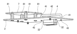
- FIG. 2 is a perspective view showing a configuration example of the second substrate 2 and the third substrate 8.
- the board-to-board connector 3 electrically connects the first board 1 and the second board 2 and, for example, the current command value of each joint from the second board 2 to the first board 1. Output to the substrate 1.
- a pair of inter-board connector 3 is provided.
- Each board-to-board connector 3 includes a first terminal 31 provided on the first board 1 and a second terminal 32 provided on the second board 2 and connected to the first terminal 31.
- the first terminal 31 is provided on the front surface 11 of the first substrate 1, for example, and the second terminal 32 is provided on the back surface 22 of the second substrate 2, for example.
- a plurality of second terminals 32 extend in the stacking direction of the first substrate 1 and the second substrate 2, that is, in the direction (downward) from the back surface 22 of the second substrate 2 toward the first substrate 1.
- a pair of inter-board connector 3 is provided, and includes a pair of first terminals 31 and a pair of second terminals 32.
- the pair of first terminals 31 are mounted parallel to each other on the front surface 11 of the first substrate 1, and the pair of second terminals 32 are also mounted parallel to each other on the back surface 22 of the second substrate 2.
- FIG. 3 is an enlarged view of a main part showing a configuration example of the robot controller 100.
- the gripping tool 4 is, for example, a handle-shaped instrument provided on the second substrate 2, and has a shape suitable for the operator to grip by hand during substrate assembly work, inspection work inside the robot controller 100, and the like. Is formed.
- the gripper 4 is provided on the surface 21 of the second substrate 2 and is disposed in the vicinity of the second terminal 32.
- the gripper 4 includes, for example, a pair of connection portions 41 erected on the surface 21 of the second substrate 2, and a grip portion 42 that connects tip ends (upper end portions) of the pair of connection portions 41 to each other.
- the grip portion 42 is a portion that is held by an assembly operator, and extends through a region A where the inter-board connector 3 is located when viewed from the normal direction of the first substrate 1.
- the region A is a region surrounding the pair of inter-board connector 3. That is, the grip portion 42 extends through the region A on a projection surface obtained by projecting the grip portion 42 and the region A onto a plane parallel to the first substrate 1 and the second substrate 2.
- a female screw (not shown) is formed at the base end portion (lower end portion) of the pair of connection portions 41 of the gripping tool 4.
- a pair of through holes (not shown) are formed in a portion where the pair of connection portions 41 of the holding tool 4 and the surface 21 of the second substrate 2 are in contact with each other.
- a pair of male screws 43 shown in FIG. 2 is inserted into the through hole from the back surface 22 of the second substrate 2 toward the front surface 21. Match. In this way, the gripping tool 4 is attached to the second substrate 2.
- the pair of spacers 5 are erected on either the front surface 11 of the first substrate 1 or the rear surface 22 of the second substrate 2, and are disposed in the vicinity of the inter-board connector 3. .
- the pair of spacers 5 are erected on the first substrate 1.
- the base end portions (lower end portions) of the pair of spacers 5 are screwed to the first substrate 1.
- the pair of spacers 5 has a base end abutting against the surface 11 of the first substrate 1 in a state where the first terminal 31 and the second terminal 32 are connected, and a tip end (upper end) of the second substrate 2.
- the length is in contact with the back surface 22.
- Each of the pair of spacers 5 has a female screw 51 formed at the tip.
- the pair of spacers 5 are disposed coaxially with the pair of through holes 23 of the second substrate 2 when viewed from the normal direction of the second substrate 2.
- the pair of female screws 51 are screwed into the pair of male screws 6 inserted into the pair of through holes 23 from the front surface 21 of the second substrate 2 toward the rear surface 22. Thereby, the second substrate 2 can be fixed to the first substrate 1.
- a plurality of spacers 82 having the same shape as the spacer 5 are erected on the first substrate 1.
- the spacer 82 has a base end (lower end) screwed to the first substrate 1 and a tip end (upper end) screwed to the second substrate 2.
- substrate 8 are arrange
- the housing 7 is formed in a box shape and includes an opening 71 formed on the upper surface, a bottom plate 72, a side wall 73, and a lid (not shown) that closes the opening 71.
- the opening 71 has a size that allows the first substrate 1 and the second substrate 2 to be inserted therethrough, and is positioned outside (above) the surface 21 of the second substrate 2.
- the first substrate 1 and the second substrate 2 are stacked and assembled on the bottom plate 72 in parallel with the bottom plate 72.
- the first substrate 1 is disposed and fixed on the bottom plate 72 via a spacer (not shown).
- the housing 7 of the robot controller 100 is configured not only horizontally as shown in FIG. 1 but also vertically. That is, the housing 7 of the robot controller 100 is configured such that any one of the four surfaces constituting the side wall 73 is positioned below and the bottom plate 72 extends in the vertical direction. Yes.
- the substrates are stacked on the casing 7 by stacking the substrates in the assembly operation of the substrates. Can be assembled. As a result, it is possible to easily perform the assembly work of the substrate, which is advantageous for automation of the assembly work using a robot, for example.
- FIG. 4 and 5 are diagrams for explaining an example of the assembly work of the substrate of the robot controller 100.
- FIG. 4 and 5 are diagrams for explaining an example of the assembly work of the substrate of the robot controller 100.
- the assembly operator grasps the grip portion 42 of the gripper 4 and inserts it into the internal space of the housing 7 from the opening 71 of the housing 7. Then, the approximate position where the second substrate 2 and the third substrate 8 are assembled is determined, and the second substrate 2 and the third substrate 8 are positioned at the determined position.
- the operator operates the gripping tool 4 to visually recognize the lower part of the through hole 23 (the direction from the second substrate 2 toward the first substrate 1) through the pair of through holes 23 as shown in FIG.
- the second substrate 2 and the third substrate 8 are positioned so that the pair of through holes 23 and the pair of female screws 51 are positioned coaxially.
- the operator operates the gripping tool 4 to keep the pair of through holes 23 and the pair of female screws 51 coaxially positioned, while the second substrate 2 and the third substrate. 8 is lowered (closer to the first substrate 1).
- the pair of second terminals 32 are inserted into the pair of first terminals 31, and the first substrate 1 and the second substrate 2 are connected via the inter-board connector 3.
- the male screw 6 is screwed into the female screw 51 of each spacer 5 to fix the second substrate 2 and the third substrate 8 to the first substrate 1.
- the second substrate 2 and the third substrate 8 can be assembled to the first substrate 1.
- the robot controller 100 can be connected to the first substrate 1 via the inter-substrate connection connector 3 by lowering the second substrate 2 and the third substrate 8. Thereby, an additional operation of connecting the substrate and the substrate with a harness can be omitted, and the assembly operation of the substrate can be performed easily and quickly.
- the gripper 4 can be gripped to perform the connection work and the connection release work of the inter-board connector 3, when the second board 2 is pushed down to insert the second terminal 32 into the first terminal 31.
- the grip portion 42 of the gripper 4 extends through the region A where the inter-board connector 3 is located when viewed from the normal direction of the first substrate 1, the inter-board connector 3 is connected.
- the force for pushing down the gripping tool 4 can be efficiently transmitted as the force for inserting the second terminal 32 into the first terminal 31.
- the force for lifting the gripper 4 when the connection between the board-to-board connectors 3 is released can be efficiently transmitted as the force for pulling the second terminal 32 out of the first terminal 31.
- the second board is adjusted by adjusting the pair of through holes 23 and the pair of female screws 51 so as to be positioned coaxially. 2 can be accurately and easily positioned with respect to the first substrate 1. Therefore, even if it is difficult to visually recognize the first terminal 31 and the second terminal 32 from the side of the space between the first substrate 1 and the second substrate 2, the first terminal 31 and the second terminal 32.
- the terminal 32 can be connected easily and reliably.
- FIG. 6 is a perspective view showing a configuration example of a robot controller 200 according to another embodiment of the present invention.
- the second substrate 202 is positioned above the first substrate 1 and arranged in a posture that intersects (more specifically, intersects with) the first substrate 1. Since the other structure of the 2nd board
- the second terminal 232 of the inter-board connector 203 extends in a direction toward the first substrate 1 from a portion facing either the first substrate 1 on the side edge of either the front surface 221 or the back surface 222 of the second substrate 202. It is provided as follows. Since the other structure of the board-to-board connector 203 is the same as that of the board-to-board connector 3, its detailed description is omitted.
- the gripping tool 204 has a connection part 241 erected on the surface 21 of the second substrate 2 and a grip part 242 extending from the tip of the connection part 241.
- the connecting portion 241 is formed in an L shape with a central portion bent, a portion on the base end side from the bent portion extends in a direction orthogonal to the second substrate 2, and a tip side portion from the bent portion is the first substrate 1. It extends in the orthogonal direction.
- the grip portion 242 extends in parallel with the first substrate 1 and the second substrate 2. Since the other configuration of the gripping tool 204 is the same as that of the gripping tool 4, detailed description thereof is omitted.
Landscapes
- Engineering & Computer Science (AREA)
- Microelectronics & Electronic Packaging (AREA)
- Robotics (AREA)
- Mechanical Engineering (AREA)
- Power Engineering (AREA)
- Combinations Of Printed Boards (AREA)
- Manipulator (AREA)
Abstract
電子回路部品を実装したプリント回路基板である第1基板(1)と、電子回路部品を実装したプリント回路基板である第2基板(2)と、第1基板に設けられた第1端子(31)と、第2基板に設けられ、第1端子に接続される第2端子(32)とを有し、第1基板と第2基板とを電気的に接続する基板間接続コネクタ(3)と、第2基板に設けられた把持具(4)と、を備える。
Description
本発明は、電子機器及びロボットコントローラに関する。
従来からプリント配線板接続構造が知られている(例えば特許文献1参照)。
このプリント配線板接続構造は、互いに平行に配置された複数の基板を接続する板間コネクタを備えている。これによって、プリント配線板接続構造をコンパクトに構成することができる。
しかし、特許文献1に記載のプリント配線板接続構造は、板間コネクタを接続及び接続解除するため、基板を押し下げたり持ち上げたりする際に基板が撓み、基板が破損する恐れが生じるという問題があった。
上記課題を解決するため、本発明のある態様に係る電子機器は、電子回路部品を実装したプリント回路基板である第1基板と、電子回路部品を実装したプリント回路基板である第2基板と、前記第1基板の設けられた第1端子と、前記第2基板に設けられ、前記第1端子に接続される第2端子とを有し、前記第1基板と前記第2基板とを電気的に接続する基板間接続コネクタと、前記第2基板に設けられた把持具と、を備える。
この構成によれば、把持具を把持して第1端子と第2端子との接続作業及び接続解除作業を行うことができる。これによって、作業時の基板の破損を防止することができる。
前記第2基板は、前記第1基板に積層配置され、前記第1端子は前記第1基板の表面に設けられ、前記第2端子は前記第2基板の裏面に設けられ、前記把持具は前記第2基板の表面に設けられていてもよい。
この構成によれば、基板の組み付け作業において、基板を積層して組み付けることができる。これによって、基板の組み付け作業を容易に行うことができ、例えば、ロボットを用いた組み付け作業の自動化に有利である。
前記基板間接続コネクタの前記第1端子及び前記第2端子の一方は前記第1基板及び前記第2基板の積層方向に伸延する電気接触部を有する雄型端子であり、前記第1端子及び前記第2端子の他方は前記雄型端子の嵌入を受容して該雄型端子の電気接触部と接触する電気接触部を有する雌型端子であってもよい。
この構成によれば、基板間接続コネクタの接続及び接続解除を容易に行うことができる。
前記把持具は、前記第1基板の法線方向から見て前記基板間接続コネクタが位置する領域を通って延在していてもよい。
この構成によれば、基板間接続コネクタの接続を行うときに、把持部を押し下げる力を第1端子及び前記第2端子の何れか一方を他方に挿し込む力として効率よく伝達することができる。また、基板間接続コネクタの接続解除を行うときに、把持部を持ち上げる力を第1端子及び第2端子の何れか一方を他方から引き抜く力として効率よく伝達することができる。
前記第1基板の表面又は前記第2基板の裏面の何れか一方に立設され、前記第1端子及び前記第2端子を接続した状態において一方の端部が前記第1基板の表面に当接し、且つ他方の端部が前記第2基板の裏面に当接する長さ寸法を有するスペーサを有していてもよい。
この構成によれば、基板間接続コネクタの接続を行うときに、第1端子及び前記第2端子の何れか一方の他方に対する挿し込み深さをスペーサによって規定することができる。これによって、基板間接続コネクタに無理な力がかかることによる基板間接続コネクタの破損を防止することができる。
前記スペーサは一対設けられていてもよい。
この構成によれば、基板間接続コネクタの接続を行うときに、第1端子及び前記第2端子の何れか一方の他方に対する挿し込み深さをスペーサによって適切に規定することができる。
前記一対のスペーサは第1基板に設けられ、前記第2基板は、前記一対のスペーサの前記他方の端部が当接する位置に位置する一対の貫通孔を有していてもよい。
この構成によれば、基板間接続コネクタの接続を行うときに、貫通孔とスペーサとが同一軸線上に位置するように調整することによって、第2基板を第1基板に対して精確に位置決めすることができる。
各前記スペーサの前記一方の端部に雌ねじが形成され、前記一対の貫通孔に挿通されて前記一対のスペーサの前記雌ねじと螺合する一対の雄ねじを有していてもよい。
この構成によれば、挿し込み深さを規定するスペーサを利用して第2基板を第1基板に適切に固定することができるので、構成を簡素なものとすることができる。
開口部を有する筐体を有し、前記開口部は、前記第1基板及び第2基板が挿通可能な大きさを有し、且つ前記第2基板の表面の外側に位置していてもよい。
この構成によれば、開口部を介して第1基板及び第2基板を筐体に組み付けることができる。
上記課題を解決するため、本発明のある態様に係るロボットコントローラは、電子回路部品を実装したプリント回路基板である第1基板と、電子回路部品を実装したプリント回路基板である第2基板と、前記第1基板の設けられた第1端子と、前記第2基板に設けられ、前記第1端子に接続される第2端子とを有し、前記第1基板と前記第2基板とを電気的に接続する基板間接続コネクタと、前記第2基板に設けられた把持具と、を備える。
この構成によれば、把持具を把持して第1端子と第2端子との接続作業及び接続解除作業を行うことができる。これによって、作業時の基板の破損を防止することができる。
本発明は、作業時の基板の破損を防止することができるという効果を奏する。
以下、本発明の実施の形態について、図面を参照しながら説明する。なお、本実施の形態によって本発明が限定されるものではない。また、以下では、全ての図を通じて、同一又は相当する要素には同一の参照符号を付して、その重複する説明を省略する。
図1は、本発明の実施の形態に係るロボットコントローラ100の構成例を示す分解斜視図である。
ロボットコントローラ100は、図示しないロボットの動作を制御する電子機器である。
図1に示すように、ロボットコントローラ100は、第1基板1と、第2基板2と、第3基板8と、基板間接続コネクタ3と、把持具4と、一対のスペーサ5と、一対の雄ねじ6と、筐体7とを含む。
第1基板1は、電子回路部品を実装したプリント回路基板である。第1基板1は、与えられた電流値指令値に基づきロボットの各関節に設けられたサーボモータに供給する電流を制御する。第1基板1は、ロボットの各関節に設けられたサーボモータに供給する比較的大きい電流、及び高い電圧の電力を扱うようパターン設計されている。第1基板1は、筐体7の後述する底板72上に底板72と平行に配置されているが、これに限られるものではない。例えば、第1基板1は、筐体7の後述する底板72上に底板72と直交する姿勢で(底板72上に立てた状態で)配置されてもよい。
第2基板2は、電子回路部品を実装したプリント回路基板である。第2基板2は、第1基板1と別体の基板であり、組み付けられた状態において、第1基板1に積層配置され、第1基板1の表面11の外方(上方)に位置するよう配設されている。なお、本実施の形態において、第2基板2は、底板72と平行に配置されている第1基板1の上方に位置するように積層配置されているが、これに限られるものではない。第1基板1が底板72上に立てた姿勢で配置されているときは、第2基板2が第1基板1の側方に位置するように積層配置されていてもよい。第2基板2の回路は、与えられた各関節の目標位置に基づき電流指令値を生成する。第2基板2は、第1基板1と比較して比較的小さい電流、及び低い電圧の電力を扱うようパターン設計されている。したがって、第1基板1及び第2基板2を別の基板で構成することにより、第1基板1の回路と第2基板2の回路との短絡を効果的に防止することができる。また、第1基板1及び第2基板2を別の基板で構成することにより、安全認証機関による第1基板1及び第2基板2に係る機器の安全認証を個別に取得することができ、一方の機器について仕様変更があった場合であっても、他の機器について再度安全認証を取得する手間を省くことができる。
第2基板2には後述する一対のスペーサ5の先端部(上端部)が当接する位置に位置する一対の貫通孔23が形成されている。一対の貫通孔23は、後述する雄ねじ6が挿通可能な径寸法を有する。
第3基板8は、電子回路部品を実装したプリント回路基板である。第3基板8は、第1基板1及び第2基板2と別体の基板であり、第1基板1及び第2基板2に積層配置され、第2基板2の上方に位置するよう配設されている。第3基板8は、動作プログラムに基づき各関節の目標位置を生成する。なお、本実施の形態において、第3基板8は、第2基板2に複数のスペーサ81を介して固定された状態で、第1基板1に組み付けられるよう構成されている。すなわち、複数のスペーサ81は、それぞれ基端部(下端部)が第2基板2に螺子止めされ、先端部(上端部)が第3基板8に螺子止めされている。
このように、ロボットコントローラ100は、第3基板8において動作プログラムに基づき目標位置を生成し出力する。そして出力された目標位置は、図示しない基板間接続コネクタ3を介して第2基板2に入力される。次に、第2基板2は、入力された各関節の目標位置に基づいて、各関節の電流指令値を生成し出力する。そして出力された電流指令値は、基板間接続コネクタ3を介して第1基板1に入力される。次に、第1基板1は、入力された各関節の電流指令値に基づいて各関節に電流を供給する。
図2は、第2基板2及び第3基板8の構成例を示す斜視図である。
図1及び図2に示すように、基板間接続コネクタ3は、第1基板1と第2基板2とを電気的に接続し、例えば、各関節の電流指令値を第2基板2から第1基板1に対して出力する。本実施の形態において、基板間接続コネクタ3は、一対設けられている。
各基板間接続コネクタ3は、第1基板1に設けられた第1端子31と、第2基板2に設けられ、第1端子31に接続される第2端子32とを含む。第1端子31は例えば第1基板1の表面11に設けられ、第2端子32は例えば第2基板2の裏面22に設けられている。基板間接続コネクタ3は、例えば、第2端子32が第1基板1及び第2基板2の積層方向、すなわち第2基板2の裏面22から第1基板1に向かう方向(下方)に伸延する複数のピン(電気接触部)を有する雄型端子であり、第1端子31が第2端子32の嵌入を受容して第2端子32の複数のピンと接触するピンソケット(電気接触部)を有する雌型端子である。したがって、第2基板2を第1基板1及び第2基板2の積層方向に下ろすことにより、第2端子32が第1端子31に挿し込まれて接続され、第2基板2を第1基板1及び第2基板2の積層方向に持ち上げることにより、第2端子32が第1端子31から引き抜かれて接続解除されるように構成されている。また、上述の通り、本実施の形態において、基板間接続コネクタ3は、一対設けられており、一対の第1端子31及び一対の第2端子32を有する。一対の第1端子31は第1基板1の表面11に互いに平行に実装され、これに対応して一対の第2端子32も第2基板2の裏面22に互いに平行に実装されている。
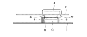
図3は、ロボットコントローラ100の構成例を示す要部拡大図である。
把持具4は、第2基板2に設けられた例えば取っ手形状の器具であり、基板の組み付け作業、ロボットコントローラ100の内部の点検作業等において、作業者が手で把持するために適した形状に形成されている。把持具4は、第2基板2の表面21に設けられ、第2端子32の近傍に配設されている。把持具4は、例えば第2基板2の表面21に立設された一対の接続部41と、一対の接続部41の先端部(上端部)を互いに接続する掴み部42とを有する。掴み部42は、組み付け作業者が把持する部分であり、図3に示すように、第1基板1の法線方向から見て基板間接続コネクタ3が位置する領域Aを通って延在する。本実施の形態において、領域Aは、一対の基板間接続コネクタ3を囲む領域である。すなわち、掴み部42及び領域Aを第1基板1及び第2基板2と平行な平面に投影した投影面において、掴み部42は領域Aを通って延在する。
把持具4の一対の接続部41の基端部(下端部)には図示しない雌ねじが形成されている。また、把持具4の一対の接続部41と第2基板2の表面21とが接触する部分には図示しない一対の貫通孔が形成されている。そして、この貫通孔に図2に示す一対の雄ねじ43が、第2基板2の裏面22から表面21に向かって挿通され、一対の雄ねじ43は把持具4の一対の接続部41の雌ねじと螺合している。このようにして、把持具4は、第2基板2に取り付けられている。
一対のスペーサ5は、図1に示すように、第1基板1の表面11又は第2基板2の裏面22の何れか一方に立設され、基板間接続コネクタ3の近傍に配設されている。本実施の形態において、一対のスペーサ5は、第1基板1に立設されている。例えば、一対のスペーサ5の基端部(下端部)は、第1基板1に螺子止めされている。
そして、一対のスペーサ5は、第1端子31及び第2端子32を接続した状態において基端部が第1基板1の表面11に当接し、且つ先端部(上端部)が第2基板2の裏面22に当接する長さ寸法を有する。
一対のスペーサ5は、それぞれ先端部に雌ねじ51が形成されている。一対のスペーサ5は、第2基板2の法線方向から見て、第2基板2の一対の貫通孔23と同軸に配設されている。そして、一対の雌ねじ51は、一対の貫通孔23に第2基板2の表面21から裏面22に向かって挿通された一対の雄ねじ6と螺合する。これによって、第2基板2を第1基板1に固定することができる。
また、例えばスペーサ5と同じ形状の複数のスペーサ82が第1基板1に立設されている。これらスペーサ82は、基端部(下端部)が第1基板1に螺子止めされ、先端部(上端部)が第2基板2に螺子止めされている。このように、第1基板1、第2基板2及び第3基板8は積層方向に互いに離間して配設され、基板間のノイズ等の影響を低減している。
筐体7は、箱状に形成され、上面に形成された開口部71と、底板72と、側壁73と、開口部71を閉塞する図示しない蓋とを含む。開口部71は、第1基板1及び第2基板2が挿通可能な大きさを有し、且つ第2基板2の表面21の外側(上方)に位置する。第1基板1及び第2基板2は、底板72の上に底板72と平行に積層されて組み付けられる。なお、第1基板1は図示しないスペーサを介して底板72上に配設、固定されている。なお、ロボットコントローラ100の筐体7は、図1に示す横置きのみならず、縦置き可能に構成されている。すなわち、ロボットコントローラ100の筐体7は、側壁73を構成する4つの面のうち何れか1つの面が下方に位置し、底板72が垂直方向に延びるように置くことができるように構成されている。
このように、第1基板1及び第2基板2は、底板72の上に底板72と平行に積層されて組み付けられるので、基板の組み付け作業において、基板を積層することによって基板を筐体7に組み付けることができる。これによって、基板の組み付け作業を容易に行うことができ、例えば、ロボットを用いた組み付け作業の自動化に有利である。
[組み付け作業例]
次に、ロボットコントローラ100の基板の組み付け作業の一例を説明する。
次に、ロボットコントローラ100の基板の組み付け作業の一例を説明する。
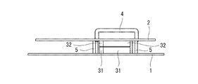
図4及び図5は、ロボットコントローラ100の基板の組み付け作業の一例を説明する図である。
第2基板2及び第3基板8をロボットコントローラ100に組み付けるときは、組み付け作業者が把持具4の掴み部42を把持して筐体7の開口部71から筐体7の内部空間に挿入し、第2基板2及び第3基板8を組み付けるおおよその位置を見定め、この見定めた位置に第2基板2及び第3基板8を位置させる。
次に、作業者は、把持具4を操作して、図3に示すように、一対の貫通孔23を通じて貫通孔23の下方(第2基板2から第1基板1に向かう方向)を視認し、一対の貫通孔23と一対の雌ねじ51とが同軸に位置するよう第2基板2及び第3基板8を位置させる。
次に、図4に示すように、作業者は、把持具4を操作して、一対の貫通孔23と一対の雌ねじ51とが同軸に位置する状態を保ちながら第2基板2及び第3基板8を下ろす(第1基板1に近づける)。これによって、一対の第2端子32が一対の第1端子31に挿し込まれ、基板間接続コネクタ3を介して第1基板1及び第2基板2が接続される。そして、各スペーサ5の雌ねじ51に雄ねじ6を螺合させ、第2基板2及び第3基板8を第1基板1に固定する。このようにして、第2基板2及び第3基板8を第1基板1に組み付けることができる。
なお、第2基板2及び第3基板8を第1基板1から取り外すときは、一対の雄ねじ6を取り外し、把持具4を把持して持ち上げる。これによって、第2端子32を第1端子31から引き抜かれ、基板間接続コネクタ3の接続が解除される。
このように、本実施の形態において、ロボットコントローラ100は、第2基板2及び第3基板8を下ろすことにより、基板間接続コネクタ3を介して第1基板1と接続することができる。これによって、基板と基板とをハーネスで接続するような追加作業を省くことができ、基板の組み付け作業を容易且つ迅速に行うことができる。
そして、把持具4を把持して基板間接続コネクタ3の接続作業及び接続解除作業を行うことができるので、第2端子32を第1端子31に挿し込むために第2基板2を押し下げたとき又は第2端子32を第1端子31から引き抜くために第2基板2を持ち上げたときに、第2基板2が撓んで破損することを防止することができる。また、作業者が基板に直接触れることによる電子回路部品の静電気破壊を防止することができる。
また、把持具4の掴み部42は、第1基板1の法線方向から見て基板間接続コネクタ3が位置する領域Aを通って延在するので、基板間接続コネクタ3の接続を行うときに、把持具4を押し下げる力を第2端子32を第1端子31に挿し込む力として効率よく伝達することができる。また、基板間接続コネクタ3の接続解除を行うときに把持具4を持ち上げる力を第2端子32を第1端子31から引き抜く力として効率よく伝達することができる。
更に、基板間接続コネクタ3の第1端子31と第2端子32とを接続するときに、一対の貫通孔23と一対の雌ねじ51とが同軸に位置するように調整することによって、第2基板2を第1基板1に対して精確且つ容易に位置決めすることができる。したがって、第1端子31及び第2端子32を第1基板1と第2基板2との間の空間の側方から視認することが困難である場合であっても、第1端子31及び第2端子32を容易且つ確実に接続することができる。
また、図5に示すように、スペーサ5の上端部と第2基板2の裏面22とが当接すると、第2基板2及び第3基板8の下方(第2基板2から第1基板1に向かう方向)への移動が規制される。これによって、第2端子32の第1端子31に対する挿し込み深さをスペーサ5によって適切に規定することができる。よって、第2端子32が第1端子31に過度に挿し込まれ、第1端子31及び第2端子32に過剰な力が加わり、第1端子31及び第2端子32が破損することを防止することができる。特に、スペーサ5は、一対設けられているので、第2端子32の第1端子31に対する挿し込み深さを一対のスペーサ5によってより適切に規定することができる。
[他の実施の形態]
図6は、本発明の他の実施の形態に係るロボットコントローラ200の構成例を示す斜視図である。
図6は、本発明の他の実施の形態に係るロボットコントローラ200の構成例を示す斜視図である。
図6に示すように、本実施の形態において、第2基板202は、第1基板1の上方に位置し、第1基板1と交差する(さらに詳しくは直交する)姿勢で配置されている。第2基板202のその他の構成は第2基板2と同様であるのでその詳細な説明を省略する。
また、基板間接続コネクタ203の第2端子232は第2基板202の表面221又は裏面222の何れか一方の側縁の第1基板1と対峙する部分から第1基板1に向かう方向に伸延するように設けられている。基板間接続コネクタ203のその他の構成は基板間接続コネクタ3と同様であるのでその詳細な説明を省略する。
また、把持具204は、第2基板2の表面21に立設された接続部241と、接続部241の先端部から延びる掴み部242とを有する。接続部241は中央部が屈曲するL字状に形成され、屈曲部分より基端側の部分は第2基板2と直交する方向に延在し、屈曲部分より先端側部分は第1基板1と直交する方向に延在している。掴み部242は、第1基板1及び第2基板2と平行に伸延している。把持具204のその他の構成は把持具4と同様であるのでその詳細な説明を省略する。
上記説明から、当業者にとっては、本発明の多くの改良や他の実施形態が明らかである。従って、上記説明は、例示としてのみ解釈されるべきであり、本発明を実行する最良の態様を当業者に教示する目的で提供されたものである。本発明の精神を逸脱することなく、その構造及び/又は機能の詳細を実質的に変更できる。
1 第1基板
2 第2基板
3 基板間接続コネクタ
4 把持具
31 (基板間接続コネクタの)第1端子
32 (基板間接続コネクタの)第2端子
100 ロボットコントローラ
2 第2基板
3 基板間接続コネクタ
4 把持具
31 (基板間接続コネクタの)第1端子
32 (基板間接続コネクタの)第2端子
100 ロボットコントローラ
Claims (10)
- 電子回路部品を実装したプリント回路基板である第1基板と、
電子回路部品を実装したプリント回路基板である第2基板と、
前記第1基板に設けられた第1端子と、前記第2基板に設けられ、前記第1端子に接続される第2端子とを有し、前記第1基板と前記第2基板とを電気的に接続する基板間接続コネクタと、
前記第2基板に設けられた把持具と、を備える、電子機器。 - 前記第2基板は、前記第1基板に積層配置され、
前記第1端子は前記第1基板の表面に設けられ、
前記第2端子は前記第2基板の裏面に設けられ、
前記把持具は前記第2基板の表面に設けられている、請求項1に記載の電子機器。 - 前記基板間接続コネクタの前記第1端子及び前記第2端子の一方は前記第1基板及び前記第2基板の積層方向に伸延する電気接触部を有する雄型端子であり、前記第1端子及び前記第2端子の他方は前記雄型端子の嵌入を受容して該雄型端子の電気接触部と接触する電気接触部を有する雌型端子である、請求項2に記載の電子機器。
- 前記把持具は、前記第1基板の法線方向から見て前記基板間接続コネクタが位置する領域を通って延在する、請求項2又は3に記載の電子機器。
- 前記第1基板の表面又は前記第2基板の裏面の何れか一方に立設され、前記第1端子及び前記第2端子を接続した状態において一方の端部が前記第1基板の表面に当接し、且つ他方の端部が前記第2基板の裏面に当接する長さ寸法を有するスペーサを有する、請求項2乃至4の何れかに記載の電子機器。
- 前記スペーサは一対設けられている、請求項5に記載の電子機器。
- 前記一対のスペーサは前記第1基板に設けられ、
前記第2基板は、前記一対のスペーサの前記他方の端部が当接する位置に位置する一対の貫通孔を有する、請求項6に記載の電子機器。 - 各前記スペーサの前記他方の端部に雌ねじが形成され、
前記一対の貫通孔に挿通されて前記一対のスペーサの前記雌ねじと螺合する一対の雄ねじを有する、請求項7に記載の電子機器。 - 開口部を有する筐体を有し、
前記開口部は、前記第1基板及び前記第2基板が挿通可能な大きさを有し、且つ前記第2基板の表面の外側に位置する、請求項1乃至8の何れかに記載の電子機器。 - 電子回路部品を実装したプリント回路基板である第1基板と、
電子回路部品を実装したプリント回路基板である第2基板と、
前記第1基板に設けられた第1端子と、前記第2基板に設けられ、前記第1端子に接続される第2端子とを有し、前記第1基板と前記第2基板とを電気的に接続する基板間接続コネクタと、
前記第2基板に設けられた把持具と、を備える、ロボットコントローラ。
Priority Applications (4)
| Application Number | Priority Date | Filing Date | Title |
|---|---|---|---|
| EP18758470.1A EP3589088B1 (en) | 2017-02-27 | 2018-02-27 | Electronic device and robot controller |
| CN201880014093.XA CN110326372B (zh) | 2017-02-27 | 2018-02-27 | 电子设备及机器人控制器 |
| KR1020197025704A KR20190112107A (ko) | 2017-02-27 | 2018-02-27 | 전자기기 및 로봇 컨트롤러 |
| US16/489,094 US10965059B2 (en) | 2017-02-27 | 2018-02-27 | Electronic device and robot controller |
Applications Claiming Priority (2)
| Application Number | Priority Date | Filing Date | Title |
|---|---|---|---|
| JP2017-035060 | 2017-02-27 | ||
| JP2017035060A JP7051297B2 (ja) | 2017-02-27 | 2017-02-27 | 電子機器及びロボットコントローラ |
Publications (1)
| Publication Number | Publication Date |
|---|---|
| WO2018155702A1 true WO2018155702A1 (ja) | 2018-08-30 |
Family
ID=63252699
Family Applications (1)
| Application Number | Title | Priority Date | Filing Date |
|---|---|---|---|
| PCT/JP2018/007140 Ceased WO2018155702A1 (ja) | 2017-02-27 | 2018-02-27 | 電子機器及びロボットコントローラ |
Country Status (6)
| Country | Link |
|---|---|
| US (1) | US10965059B2 (ja) |
| EP (1) | EP3589088B1 (ja) |
| JP (1) | JP7051297B2 (ja) |
| KR (1) | KR20190112107A (ja) |
| CN (1) | CN110326372B (ja) |
| WO (1) | WO2018155702A1 (ja) |
Families Citing this family (12)
| Publication number | Priority date | Publication date | Assignee | Title |
|---|---|---|---|---|
| DE202018104586U1 (de) * | 2018-08-09 | 2019-11-19 | Sma Solar Technology Ag | Zwischenkreisanordnung und Wechselrichter |
| JP7384618B2 (ja) * | 2019-10-23 | 2023-11-21 | ファナック株式会社 | 接続構造および組立体 |
| US11357103B1 (en) * | 2020-01-21 | 2022-06-07 | Signetik, LLC | System-in-package cellular assembly |
| DE102020208631A1 (de) * | 2020-07-09 | 2022-01-13 | Robert Bosch Gesellschaft mit beschränkter Haftung | Elektronikeinheit für ein Elektrogerät |
| CN111682331A (zh) * | 2020-08-17 | 2020-09-18 | 深圳微步信息股份有限公司 | 多功能扩展电路板模块及移动终端 |
| US12095189B2 (en) * | 2020-12-24 | 2024-09-17 | Intel Corporation | Ultra slim module form factor and connector architecture for top mount connection |
| CN113286447B (zh) * | 2021-05-06 | 2022-09-02 | 成都哈工驱动科技有限公司 | 一种具有铜鸡眼结构伺服驱动器的加工工艺 |
| JP7758522B2 (ja) * | 2021-09-28 | 2025-10-22 | TE Connectivity Japan合同会社 | ソケット |
| JP2023058113A (ja) * | 2021-10-13 | 2023-04-25 | 株式会社Jvcケンウッド | 筐体構造 |
| CN114221160A (zh) * | 2021-11-10 | 2022-03-22 | 北京无线电测量研究所 | 一种测试工装及其制作方法 |
| JP7816049B2 (ja) * | 2022-09-08 | 2026-02-18 | サクサ株式会社 | 基板の着脱部材および基板の着脱構造 |
| US12432855B2 (en) * | 2023-03-07 | 2025-09-30 | SanDisk Technologies, Inc. | Multiple circuit board assembly including a support element and method of manufacture thereof |
Citations (6)
| Publication number | Priority date | Publication date | Assignee | Title |
|---|---|---|---|---|
| JPS5996888U (ja) * | 1982-12-20 | 1984-06-30 | 日本電気株式会社 | 電子機器収容装置 |
| JPH0395571U (ja) * | 1990-01-19 | 1991-09-30 | ||
| JPH0432292A (ja) * | 1990-05-29 | 1992-02-04 | Mitsubishi Electric Corp | 印刷配線板の接続構造 |
| JPH04102594U (ja) * | 1991-02-01 | 1992-09-03 | 富士通テン株式会社 | 多層基板の着脱機構 |
| JP2005150161A (ja) | 2003-11-11 | 2005-06-09 | Canon Inc | プリント配線板接続構造 |
| JP2011134868A (ja) * | 2009-12-24 | 2011-07-07 | Yamaha Corp | プリント回路板取付構造 |
Family Cites Families (10)
| Publication number | Priority date | Publication date | Assignee | Title |
|---|---|---|---|---|
| US4546414A (en) * | 1983-04-12 | 1985-10-08 | Nordson Corporation | Plug-in circuit board connector and keying assembly |
| US4620362A (en) * | 1984-06-22 | 1986-11-04 | The Boeing Company | Changeable tooling system for robot end-effector |
| JPS62283696A (ja) * | 1986-06-02 | 1987-12-09 | キヤノン株式会社 | プリント基板 |
| US5425133A (en) * | 1990-01-24 | 1995-06-13 | Canon Kabushiki Kaisha | Robot apparatus with an electrical driver for controlling a detachable rotor hand |
| US5205701A (en) * | 1990-06-04 | 1993-04-27 | Canon Kabushiki Kaisha | Industrial robot |
| JPH08330699A (ja) * | 1995-05-30 | 1996-12-13 | Nec Corp | プリント配線基板及びその間の実装方式 |
| JPH11135910A (ja) * | 1997-10-31 | 1999-05-21 | Fujitsu Ltd | プリント板のシエルフ実装構造 |
| JP2003188489A (ja) * | 2001-12-14 | 2003-07-04 | Pentax Corp | 電子スコープの基板構造 |
| US9740249B2 (en) * | 2014-01-30 | 2017-08-22 | Hewlett Packard Enterprise Development Lp | Mounting device |
| JP2015157154A (ja) | 2015-06-08 | 2015-09-03 | 株式会社大都技研 | 遊技台 |
-
2017
- 2017-02-27 JP JP2017035060A patent/JP7051297B2/ja active Active
-
2018
- 2018-02-27 US US16/489,094 patent/US10965059B2/en active Active
- 2018-02-27 WO PCT/JP2018/007140 patent/WO2018155702A1/ja not_active Ceased
- 2018-02-27 CN CN201880014093.XA patent/CN110326372B/zh active Active
- 2018-02-27 KR KR1020197025704A patent/KR20190112107A/ko not_active Ceased
- 2018-02-27 EP EP18758470.1A patent/EP3589088B1/en active Active
Patent Citations (6)
| Publication number | Priority date | Publication date | Assignee | Title |
|---|---|---|---|---|
| JPS5996888U (ja) * | 1982-12-20 | 1984-06-30 | 日本電気株式会社 | 電子機器収容装置 |
| JPH0395571U (ja) * | 1990-01-19 | 1991-09-30 | ||
| JPH0432292A (ja) * | 1990-05-29 | 1992-02-04 | Mitsubishi Electric Corp | 印刷配線板の接続構造 |
| JPH04102594U (ja) * | 1991-02-01 | 1992-09-03 | 富士通テン株式会社 | 多層基板の着脱機構 |
| JP2005150161A (ja) | 2003-11-11 | 2005-06-09 | Canon Inc | プリント配線板接続構造 |
| JP2011134868A (ja) * | 2009-12-24 | 2011-07-07 | Yamaha Corp | プリント回路板取付構造 |
Non-Patent Citations (1)
| Title |
|---|
| See also references of EP3589088A4 |
Also Published As
| Publication number | Publication date |
|---|---|
| KR20190112107A (ko) | 2019-10-02 |
| CN110326372B (zh) | 2022-12-30 |
| US10965059B2 (en) | 2021-03-30 |
| JP7051297B2 (ja) | 2022-04-11 |
| EP3589088A1 (en) | 2020-01-01 |
| CN110326372A (zh) | 2019-10-11 |
| EP3589088A4 (en) | 2020-12-30 |
| US20200076124A1 (en) | 2020-03-05 |
| JP2018142587A (ja) | 2018-09-13 |
| EP3589088B1 (en) | 2023-04-12 |
Similar Documents
| Publication | Publication Date | Title |
|---|---|---|
| WO2018155702A1 (ja) | 電子機器及びロボットコントローラ | |
| US20160329647A1 (en) | Cable holding member, plug connector, connector device, flat cable, and method for assembling plug connector | |
| JP6627683B2 (ja) | 電気機器 | |
| JP2009076454A (ja) | 電気コネクタ | |
| JP2016046005A (ja) | コネクタ | |
| US20190387625A1 (en) | Electric product | |
| EP3319177B1 (en) | Modularized structure of switch wire connection device | |
| CN102332661B (zh) | 用于在电路板上保持模块的对准销 | |
| JP2010003933A (ja) | フレキシブルプリント基板及びこれを電子機器内に保持する方法 | |
| JP2013030291A (ja) | コネクタ保持構造、電子機器、電動機制御装置 | |
| EP4465776A2 (en) | Pcb connector | |
| JP7184440B2 (ja) | 板状部材の結合構造、電子機器、およびコネクタの着脱方法 | |
| JP2021019132A (ja) | 回路基板の取り外し方法 | |
| US20120309223A1 (en) | Guide element for a connector device | |
| CN101292398A (zh) | 电接触元件 | |
| JP2017135185A (ja) | 電子制御装置 | |
| WO2011018825A1 (ja) | 接続コネクタの位置決め接続装置 | |
| JP2020155693A (ja) | 接続部材及びコネクター部材 | |
| JP2017130329A (ja) | コネクタ及びコネクタユニット | |
| JP6657656B2 (ja) | ロボット制御装置、ロボット、ロボットシステム | |
| JP5810783B2 (ja) | 端子部材及び電子機器 | |
| JP2009193918A (ja) | コネクタの挿抜構造 | |
| CN100466427C (zh) | 电源装置 | |
| JP2014078404A (ja) | 着脱式端子装置 | |
| KR19980058787U (ko) | 교육용 회로보드 결합장치 |
Legal Events
| Date | Code | Title | Description |
|---|---|---|---|
| 121 | Ep: the epo has been informed by wipo that ep was designated in this application |
Ref document number: 18758470 Country of ref document: EP Kind code of ref document: A1 |
|
| NENP | Non-entry into the national phase |
Ref country code: DE |
|
| ENP | Entry into the national phase |
Ref document number: 20197025704 Country of ref document: KR Kind code of ref document: A |
|
| WWE | Wipo information: entry into national phase |
Ref document number: 2018758470 Country of ref document: EP |