WO2018190205A1 - 固体電解質集積素子、固体電解質集積素子の製造方法、及び、固体電解質素子 - Google Patents
固体電解質集積素子、固体電解質集積素子の製造方法、及び、固体電解質素子 Download PDFInfo
- Publication number
- WO2018190205A1 WO2018190205A1 PCT/JP2018/014331 JP2018014331W WO2018190205A1 WO 2018190205 A1 WO2018190205 A1 WO 2018190205A1 JP 2018014331 W JP2018014331 W JP 2018014331W WO 2018190205 A1 WO2018190205 A1 WO 2018190205A1
- Authority
- WO
- WIPO (PCT)
- Prior art keywords
- electrode layer
- solid electrolyte
- lower electrode
- main surface
- layer
- Prior art date
- Legal status (The legal status is an assumption and is not a legal conclusion. Google has not performed a legal analysis and makes no representation as to the accuracy of the status listed.)
- Ceased
Links
Images









Classifications
-
- G—PHYSICS
- G01—MEASURING; TESTING
- G01N—INVESTIGATING OR ANALYSING MATERIALS BY DETERMINING THEIR CHEMICAL OR PHYSICAL PROPERTIES
- G01N27/00—Investigating or analysing materials by the use of electric, electrochemical, or magnetic means
- G01N27/26—Investigating or analysing materials by the use of electric, electrochemical, or magnetic means by investigating electrochemical variables; by using electrolysis or electrophoresis
- G01N27/403—Cells and electrode assemblies
- G01N27/406—Cells and probes with solid electrolytes
- G01N27/407—Cells and probes with solid electrolytes for investigating or analysing gases
-
- H—ELECTRICITY
- H01—ELECTRIC ELEMENTS
- H01M—PROCESSES OR MEANS, e.g. BATTERIES, FOR THE DIRECT CONVERSION OF CHEMICAL ENERGY INTO ELECTRICAL ENERGY
- H01M10/00—Secondary cells; Manufacture thereof
- H01M10/05—Accumulators with non-aqueous electrolyte
- H01M10/056—Accumulators with non-aqueous electrolyte characterised by the materials used as electrolytes, e.g. mixed inorganic/organic electrolytes
- H01M10/0561—Accumulators with non-aqueous electrolyte characterised by the materials used as electrolytes, e.g. mixed inorganic/organic electrolytes the electrolyte being constituted of inorganic materials only
- H01M10/0562—Solid materials
-
- C—CHEMISTRY; METALLURGY
- C25—ELECTROLYTIC OR ELECTROPHORETIC PROCESSES; APPARATUS THEREFOR
- C25B—ELECTROLYTIC OR ELECTROPHORETIC PROCESSES FOR THE PRODUCTION OF COMPOUNDS OR NON-METALS; APPARATUS THEREFOR
- C25B9/00—Cells or assemblies of cells; Constructional parts of cells; Assemblies of constructional parts, e.g. electrode-diaphragm assemblies; Process-related cell features
- C25B9/17—Cells comprising dimensionally-stable non-movable electrodes; Assemblies of constructional parts thereof
- C25B9/19—Cells comprising dimensionally-stable non-movable electrodes; Assemblies of constructional parts thereof with diaphragms
- C25B9/23—Cells comprising dimensionally-stable non-movable electrodes; Assemblies of constructional parts thereof with diaphragms comprising ion-exchange membranes in or on which electrode material is embedded
-
- B—PERFORMING OPERATIONS; TRANSPORTING
- B01—PHYSICAL OR CHEMICAL PROCESSES OR APPARATUS IN GENERAL
- B01D—SEPARATION
- B01D2256/00—Main component in the product gas stream after treatment
- B01D2256/12—Oxygen
-
- B—PERFORMING OPERATIONS; TRANSPORTING
- B01—PHYSICAL OR CHEMICAL PROCESSES OR APPARATUS IN GENERAL
- B01D—SEPARATION
- B01D2256/00—Main component in the product gas stream after treatment
- B01D2256/16—Hydrogen
-
- B—PERFORMING OPERATIONS; TRANSPORTING
- B01—PHYSICAL OR CHEMICAL PROCESSES OR APPARATUS IN GENERAL
- B01D—SEPARATION
- B01D2259/00—Type of treatment
- B01D2259/45—Gas separation or purification devices adapted for specific applications
- B01D2259/4533—Gas separation or purification devices adapted for specific applications for medical purposes
-
- B—PERFORMING OPERATIONS; TRANSPORTING
- B01—PHYSICAL OR CHEMICAL PROCESSES OR APPARATUS IN GENERAL
- B01D—SEPARATION
- B01D53/00—Separation of gases or vapours; Recovering vapours of volatile solvents from gases; Chemical or biological purification of waste gases, e.g. engine exhaust gases, smoke, fumes, flue gases, aerosols
- B01D53/32—Separation of gases or vapours; Recovering vapours of volatile solvents from gases; Chemical or biological purification of waste gases, e.g. engine exhaust gases, smoke, fumes, flue gases, aerosols by electrical effects other than those provided for in group B01D61/00
- B01D53/326—Separation of gases or vapours; Recovering vapours of volatile solvents from gases; Chemical or biological purification of waste gases, e.g. engine exhaust gases, smoke, fumes, flue gases, aerosols by electrical effects other than those provided for in group B01D61/00 in electrochemical cells
-
- C—CHEMISTRY; METALLURGY
- C25—ELECTROLYTIC OR ELECTROPHORETIC PROCESSES; APPARATUS THEREFOR
- C25B—ELECTROLYTIC OR ELECTROPHORETIC PROCESSES FOR THE PRODUCTION OF COMPOUNDS OR NON-METALS; APPARATUS THEREFOR
- C25B1/00—Electrolytic production of inorganic compounds or non-metals
- C25B1/01—Products
- C25B1/02—Hydrogen or oxygen
-
- Y—GENERAL TAGGING OF NEW TECHNOLOGICAL DEVELOPMENTS; GENERAL TAGGING OF CROSS-SECTIONAL TECHNOLOGIES SPANNING OVER SEVERAL SECTIONS OF THE IPC; TECHNICAL SUBJECTS COVERED BY FORMER USPC CROSS-REFERENCE ART COLLECTIONS [XRACs] AND DIGESTS
- Y02—TECHNOLOGIES OR APPLICATIONS FOR MITIGATION OR ADAPTATION AGAINST CLIMATE CHANGE
- Y02E—REDUCTION OF GREENHOUSE GAS [GHG] EMISSIONS, RELATED TO ENERGY GENERATION, TRANSMISSION OR DISTRIBUTION
- Y02E60/00—Enabling technologies; Technologies with a potential or indirect contribution to GHG emissions mitigation
- Y02E60/10—Energy storage using batteries
Definitions
- the present invention relates to a solid electrolyte integrated element, a method for manufacturing a solid electrolyte integrated element, and a solid electrolyte element.
- solid electrolyte elements are used in oxygen sensors, oxygen concentrators, and the like.
- Patent Document 1 discloses a structure in which a through hole is formed in a solid electrolyte layer and a plurality of electrodes are connected in series through the through hole.
- this structure there is a problem that stress is applied to the solid electrolyte layer provided with the through holes, and the solid electrolyte integrated element collapses.
- Patent Document 2 discloses a structure of an electrochemical cell in which a plurality of solid electrolyte elements are fixed to positioning protrusions and joined in series. As a result, it is not necessary to provide a clearance for connection wiring between the electrochemical cells, so that compactness can be achieved. However, in the structure described in Patent Document 2, there is a problem that stress is applied when the protrusion and the solid electrolyte element are joined, and the solid electrolyte element is damaged.
- Patent Document 3 the upper substrate is anodically bonded to a laminate of electrodes / solid electrolyte / electrodes laminated on a dummy silicon substrate, the dummy silicon substrate is removed by wet etching, and then the lower substrate is anodically bonded.
- a method of manufacturing an element in which a thin film (solid electrolyte layer) of a solid electrolyte is sandwiched between two substrates is disclosed.
- the lower substrate is joined to the solid electrolyte layer, stress is applied to the solid electrolyte layer, so that the solid electrolyte layer is damaged.
- an object of the present invention is to provide a solid electrolyte integrated device capable of reducing the stress applied to the solid electrolyte layer while reducing the current.
- a solid electrolyte integrated device is a solid electrolyte integrated device including a substrate having an insulating surface, and the substrate has a first main surface on one surface side thereof, and A first main surface and a second main surface provided on the back side of the first main surface, the first and second through holes penetrating between the first main surface and the second main surface.
- the solid electrolyte integrated element is provided on the first main surface so as to cover or rim part of the first opening on the first main surface side of the first through hole.
- a first lower electrode layer having conductivity; a first solid electrolyte layer electrically connected on the first lower electrode layer; and the first solid electrolyte layer provided on the first main surface side.
- first upper electrode layer spaced apart from the first lower electrode layer and electrically connected to the first solid electrolyte layer
- a conductive second lower electrode layer provided on the first main surface so as to cover or rim part of the second opening on the first main surface side of the two through holes
- a second solid electrolyte layer provided on the lower electrode layer and spaced apart from the first solid electrolyte layer and electrically connected to the second lower electrode layer; and provided on the first main surface side.
- Each of the electrode layers is permeable to ions and / or has ion redox ability, and metal Ku are those containing either or both of a metal oxide, and has a vent for further aeration.
- the solid electrolyte integrated element, the method for manufacturing a solid electrolyte integrated element, and the solid electrolyte element according to one embodiment of the present invention can reduce mechanical stress applied to the solid electrolyte layer.
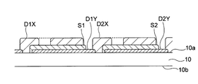
- FIG. 1 is a cross-sectional view showing an example of a solid electrolyte integrated device 100 according to the first embodiment.
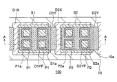
- FIG. 2 is a plan view of the configuration in the vicinity of the plane along the first main surface 10a of the substrate 10 of the solid electrolyte integrated device 100 shown in FIG. 1 as viewed from below.
- FIG. 3 is a plan view showing an example of a configuration of a solid electrolyte integrated element in which a plurality of solid electrolyte integrated elements are connected in series.
- FIG. 4 is a plan view showing another example of the configuration of the solid electrolyte integrated element in which a plurality of solid electrolyte integrated elements are connected in series.
- FIG. 1 is a cross-sectional view showing an example of a solid electrolyte integrated device 100 according to the first embodiment.
- FIG. 2 is a plan view of the configuration in the vicinity of the plane along the first main surface 10a of the substrate 10 of the solid electrolyte integrated device 100 shown in FIG. 1 as viewed from
- FIG. 5 is a plan view showing still another example of the configuration of the solid electrolyte integrated element in which a plurality of solid electrolyte integrated elements are connected in series.
- FIG. 6 is a cross-sectional view showing an example of the solid electrolyte integrated device 100 according to the first modification.
- FIG. 7 is a plan view of the configuration in the vicinity of the plane along the first main surface 10a of the substrate 10 of the solid electrolyte integrated device 100 shown in FIG. 6, as viewed from below.
- FIG. 8 is a cross-sectional view showing an example of the solid electrolyte integrated device 100 according to the second modification.
- FIG. 9 is a plan view of the configuration in the vicinity of the plane along the first main surface 10a of the substrate 10 of the solid electrolyte integrated device 100 shown in FIG.
- FIG. 10 is a cross-sectional view showing an example of the solid electrolyte integrated device 100 according to the third modification.
- FIG. 11 is a plan view of the configuration in the vicinity of the plane along the first main surface 10a of the substrate 10 of the solid electrolyte integrated device 100 shown in FIG. 10 as viewed from below.
- FIG. 12 is a cross-sectional view showing an example of the steps of the method for manufacturing the solid electrolyte integrated device 100 of Modification 1 shown in FIG.
- FIG. 13 is a cross-sectional view showing the steps of the method of manufacturing solid electrolyte integrated device 100 subsequent to FIG.
- FIG. 14 is a cross-sectional view showing the steps of the method for manufacturing the solid electrolyte integrated device 100 subsequent to FIG. 13.
- FIG. 13 is a cross-sectional view showing the steps of the method for manufacturing the solid electrolyte integrated device 100 subsequent to FIG. 13.
- FIG. 13 is a cross-sectional view showing the steps of the method for manufacturing the solid electrolyte integrated device
- FIG. 15 is a cross-sectional view showing the steps of the method for manufacturing the solid electrolyte integrated device 100 subsequent to FIG.
- FIG. 16 is a cross-sectional view showing the steps of the method of manufacturing solid electrolyte integrated device 100 subsequent to FIG. 17 is a cross-sectional view showing another example of the process of the method for manufacturing the solid electrolyte integrated device 100 of Modification 1 shown in FIG.
- FIG. 18 is a cross-sectional view showing the steps of the method of manufacturing solid electrolyte integrated device 100 subsequent to FIG.
- FIG. 19 is a cross-sectional view showing the steps of the method for manufacturing the solid electrolyte integrated device 100 subsequent to FIG.
- FIG. 20 is a cross-sectional view showing the steps of the method of manufacturing solid electrolyte integrated device 100 following FIG.
- FIG. 21 is a cross-sectional view showing the steps of the method of manufacturing solid electrolyte integrated device 100 subsequent to FIG.
- FIG. 22 is a cross-sectional view showing the steps of the method for manufacturing the solid electrolyte integrated device 100 subsequent to FIG.
- FIG. 23 is a cross-sectional view showing the steps of the method of manufacturing solid electrolyte integrated device 100 following FIG.
- FIG. 24 is a cross-sectional view showing the steps of the method of manufacturing solid electrolyte integrated device 100 subsequent to FIG.
- FIG. 25 is a cross-sectional view showing an example of the solid electrolyte integrated device 100 according to the second embodiment.
- FIG. 21 is a cross-sectional view showing the steps of the method of manufacturing solid electrolyte integrated device 100 subsequent to FIG.
- FIG. 22 is a cross-sectional view showing the steps of the method for manufacturing the solid electrolyte integrated device 100 subsequent to FIG.
- FIG. 23 is a cross-sectional view showing the steps of the method of manufacturing solid electrolyt
- FIG. 26 is a cross-sectional view showing an example of the steps of the method for manufacturing the solid electrolyte integrated device 100 according to the second embodiment shown in FIG.
- FIG. 27 is a cross-sectional view showing the steps of the method of manufacturing solid electrolyte integrated device 100 following FIG.
- FIG. 28 is a cross-sectional view showing the steps of the method of manufacturing solid electrolyte integrated device 100 subsequent to FIG.
- FIG. 29 is a cross-sectional view showing the steps of the method of manufacturing solid electrolyte integrated device 100 following FIG.
- FIG. 30 is a cross-sectional view showing the steps of the method for manufacturing the solid electrolyte integrated device 100 subsequent to FIG.
- FIG. 1 is a cross-sectional view showing an example of a solid electrolyte integrated device 100 according to the first embodiment.
- FIG. 2 is a plan view of the configuration in the vicinity of the plane along the first main surface 10a of the substrate 10 of the solid electrolyte integrated device 100 shown in FIG. 1 as viewed from below.
- the cross section in FIG. 1 corresponds to the cross section along the line AA in FIG.
- the direction from the second main surface 10b to the first main surface 10a of the substrate 10 is defined as the upward direction with respect to the position of the substrate 10 of the solid electrolyte integrated device 100 as a reference.
- the direction from the main surface 10a to the second main surface 10b is a downward direction.
- substrate 10 is made into the upper side (upward), and the 2nd main surface 10b side of the said board
- a solid electrolyte integrated device 100 in which a plurality of solid electrolyte layers (solid electrolyte layers) according to the present embodiment are integrated includes a substrate 10, a first lower electrode layer D1Y, The first solid electrolyte layer S1, the first upper electrode layer D1X, the first additional electrode layer D1A, the second lower electrode layer D2Y, the second solid electrolyte layer S2, the second upper electrode layer D2X, 2 additional electrode layers D2A.
- the electrode connected to the upper surface of the first (second) solid electrolyte layer S1 (S2) is a first electrode with the position of the first (second) solid electrolyte layer S1 (S2) of the solid electrolyte integrated device 100 as a reference. 1 (second) upper electrode layer D1X (D2X), and an electrode connected to the lower surface of the first (second) solid electrolyte layer S1 (S2) as first (second) lower electrode layer D1Y (D2Y) Yes.
- the solid electrolyte integrated device 100 is applied to, for example, an oxygen concentrator or a hydrogen production device.
- the substrate 10, the first lower electrode layer D1Y, the first solid electrolyte layer S1, and the first upper electrode layer D1X constitute one solid electrolyte element. Then, a plurality of such solid electrolyte elements are electrically connected in series (in the example of FIG. 1, focusing attention on two minimum units), the solid electrolyte integrated element 100 is configured. Is done. Hereinafter, each configuration of the solid electrolyte integrated element 100 will be described.
- the substrate 10 has a first main surface 10a on one surface and a second main surface 10b on the back surface side of the first main surface 10a.
- the substrate 10 is provided with a first through hole P1 and a second through hole P2 penetrating between the first main surface 10a and the second main surface 10b.
- the first through hole P1 and the second through hole P2 of the substrate 10 allow gas to flow between the first main surface 10a and the second main surface 10b.
- the substrate 10 has an insulating surface.
- the substrate 10 is made of glass.
- the substrate 10 may be a silicon substrate having silicon oxide on the outer surface.
- the outer surface of the substrate 10 is a concept including the first and second main surfaces 10 a and 10 b and the side surfaces of the substrate 10.
- the substrate 10 has an insulating property on the outer surface so that no current flows through the substrate 10 itself.
- the material of the substrate 10 is excellent in heat resistance and electrical insulation, such as glass, silicon coated with an oxide, oxide-coated metal (Ti, Ni or alloys), oxide ceramics ( Al 2 O 3 , zirconia, magnesia, lanthanum chromite, etc.) may be selected.
- glass or silicon covered with an oxide is more preferably selected.
- silicon coated with an oxide is selected as a material superior in material cost and manufacturing cost.
- first through holes P ⁇ b> 1 and two second through holes P ⁇ b> 2 there are four first through holes P ⁇ b> 1 and two second through holes P ⁇ b> 2, but there are one or more first through holes P ⁇ b> 1 and second through holes P ⁇ b> 2. Three or five or more may be sufficient.
- the thickness of the substrate 10 is preferably in the range of 50 ⁇ m to 3000 ⁇ m, for example, from the viewpoint of supporting each layer formed on the substrate 10 and the ability to easily form a through hole.
- substrate 10 have circular shape seeing from the 1st main surface side, for example.
- the diameter of the circular shape of the first and second through holes P1 and P2 is, for example, in the range of 0.01 mm to 30 mm.
- the first and second through holes P1 and P2 of the substrate 10 may have, for example, a rectangle other than a circle or a polygon such as a hexagon as viewed from the first main surface side. .
- First lower electrode layer D1Y is, for example, as shown in FIG. 1, the first main surface 10a so as to cover a part of the first opening P1a on the first main surface 10a side of the first through hole P1. It is provided above.
- the first lower electrode layer D1Y covers a part of the first opening P1a, so that the potential of the first opening P1a can be controlled to a predetermined value.
- the first lower electrode layer D1Y has conductivity.
- the first lower electrode layer D1Y transmits ions and / or has ion redox capability.
- the first lower electrode layer D1Y has a first main surface so as to frame a part of the first opening P1a on the first main surface 10a side of the first through hole P1. 10a may be provided.
- the first lower electrode layer D1Y has a third through hole D1YP that penetrates the first lower electrode layer D1Y in the vertical direction and communicates with the first through hole P1 of the substrate 10. Is provided.
- the third through hole D1YP of the first lower electrode layer D1Y is filled with a part S1P of the first solid electrolyte layer S1.
- the first lower electrode layer D1Y includes, for example, either a metal or a metal oxide, or both, and may have a ventilation portion (not shown) for venting.
- the ventilation portion has a shape that allows the gas on the first through hole P1 side of the first lower electrode layer D1Y to vent to the interface with the first solid electrolyte layer S1.
- the ventilation portion may have a mesh shape or a porous shape.
- the first lower electrode layer D1Y preferably has a thickness in the range of 0.01 to 1000 ⁇ m.
- First solid electrolyte layer S1 Further, the first solid electrolyte layer S1 is provided on the first lower electrode layer D1Y, for example, as shown in FIG. The first solid electrolyte layer S1 is electrically connected to the first lower electrode layer D1Y. An intermediate layer (not shown) having ion conductivity may be provided between the first solid electrolyte layer S1 and the first lower electrode layer D1Y.
- the first solid electrolyte layer S1 covers the upper surface D1Ya of the first lower electrode layer D1Y and a part of the side surface D1Yb. Thereby, the contact resistance between 1st solid electrolyte layer S1 and 1st lower electrode layer D1Y is reduced.
- the first solid electrolyte layer S1 has a part of the side surface S1X covered with the first upper electrode layer D1X.
- the first upper electrode layer D1X covers the first solid electrolyte layer S1 from the upper surface S1a to a part of the side surface S1X.
- the first solid electrolyte layer S1 is electrically connected to the first upper electrode layer D1X, and the contact resistance between the first solid electrolyte layer S1 and the first upper electrode layer D1X is reduced. It has become.
- An intermediate layer (not shown) having electron-ion conductivity may be provided between the first solid electrolyte layer S1 and the first upper electrode layer D1X.
- this 1st solid electrolyte layer S1 is ion-conductive, for example, has proton conductivity, carbonate ion conductivity, or oxide ion conductivity.
- the first solid electrolyte layer S1 has oxide ion conductivity.
- the first solid electrolyte layer S1 has an oxide ion conductivity of 1.0 ⁇ 10 ⁇ 3 S / cm in an atmosphere of 600 °, for example.
- the first solid electrolyte layer S1 preferably has a thickness on the first lower electrode layer D1Y in the range of 0.05 ⁇ m to 300 ⁇ m.
- First upper electrode layer D1X is provided on the first main surface 10a side so as to be separated from the first lower electrode layer D1Y via the first solid electrolyte layer S1.
- the first upper electrode layer D1X is electrically connected to the first solid electrolyte layer S1 and has conductivity.
- the first upper electrode layer D1X transmits ions and / or has ion redox ability.
- the first upper electrode layer D1X includes, for example, either a metal or a metal oxide, or both, and may have a ventilation portion (not shown) for venting.
- the ventilation portion has a shape in which the gas on the surface of the first upper electrode layer D1X can be vented to the interface with the first solid electrolyte layer S1.
- the ventilation portion may have a mesh shape or a porous shape.
- the thickness of the first upper electrode layer D1X on the first solid electrolyte layer S1 is preferably in the range of 0.01 ⁇ m to 300 ⁇ m.
- First additional electrode layer D1A arbitrary layer
- the first additional electrode layer D1A is provided in the vicinity of the first opening P1a in the first through hole P1 and electrically connected to the first lower electrode layer D1Y, for example, as shown in FIG. ing.
- the resistance value including the first lower electrode layer D1Y electrically connected to the first additional electrode layer D1A is lowered, and the electric power between the first additional electrode layer D1A and the first solid electrolyte layer S1 is reduced. Contact resistance can be reduced.
- the first additional electrode layer D1A preferably has a thickness in the range of 0.01 ⁇ m to 300 ⁇ m.
- first additional electrode layer D1A may not be provided.
- the surface of the first lower electrode layer D1Y is exposed to the first through hole P1 side.
- Second lower electrode layer D2Y The second lower electrode layer D2Y is provided on the first main surface 10a so as to cover a part of the second opening P2a on the first main surface 10a side of the second through hole P2.
- the second lower electrode layer D2Y covers a part of the second opening P2a, so that the potential of the second opening P2a can be controlled to a predetermined value.
- this 2nd lower electrode layer D2Y has electroconductivity.
- the second lower electrode layer D2Y transmits ions and / or has an ion redox ability.
- the second lower electrode layer D2Y has a first main surface that borders a part of the second opening P2a on the first main surface 10a side of the second through hole P2. 10a may be provided.
- the second lower electrode layer D2Y has a fourth through hole D2YP that penetrates the second lower electrode layer D2Y in the vertical direction and communicates with the second through hole P2 of the substrate 10. Is provided. Furthermore, a part S2P of the second solid electrolyte layer S2 is filled in the fourth through hole D2YP of the second lower electrode layer D2Y. Thereby, the resistance value of the second solid electrolyte layer S2 itself can be lowered, and the contact resistance between the second solid electrolyte layer S2 and the second lower electrode layer D2Y can be reduced.
- the second lower electrode layer D2Y has the same configuration as the first lower electrode layer D1Y described above, and includes, for example, either a metal or a metal oxide, or both, and allows ventilation. You may have a ventilation part (not shown).
- the second lower electrode layer D2Y preferably has a thickness in the range of 0.01 to 1000 ⁇ m.
- any material having electrical conductivity can be used without particular limitation.
- Pt, Pd , Ag, Au, W, Mo, Ta, Nb, Ni, etc., and alloys containing these metals metallic electronic conductor materials such as stainless steel, lanthanum strontium cobalt ferrite (LSCF), barium ferrite, cobalt manganese oxide , Ceramic oxygen-electron mixed conductors such as lanthanum nickelates, transparent electrode materials such as tin oxides such as ITO and FTO and zinc oxides such as AZO and GZO, mixtures and supports of these materials, Examples thereof include, but are not limited to, cermet mixed with the solid electrolyte.
- Second solid electrolyte layer S2 Further, for example, as shown in FIG. 1, the second solid electrolyte layer S2 is separated (not electrically directly connected) from the first solid electrolyte layer S1 described above on the second lower electrode layer D2Y. , Provided. The second solid electrolyte layer S2 is electrically connected to the second lower electrode layer D2Y. An intermediate layer (not shown) having electron-ion conductivity may be provided between the second solid electrolyte layer S2 and the second lower electrode layer D2Y.
- the second solid electrolyte layer S2 covers the upper surface D2Ya of the second lower electrode layer D2Y to a part of the side surface D2Yb. Thereby, the contact resistance between 2nd solid electrolyte layer S2 and 2nd lower electrode layer D2Y is reduced.
- the second solid electrolyte layer S2 has a part of the side surface S2X covered with the second upper electrode layer D2X.
- the second upper electrode layer D2X covers, for example, from the upper surface S2a of the second solid electrolyte layer S2 to a part of the side surface S2X, as shown in FIG.
- the second solid electrolyte layer S2 is electrically connected to the second upper electrode layer D2X.
- the second solid electrolyte layer S2 is interposed between the second solid electrolyte layer S2 and the first upper electrode layer D2X. Contact resistance is reduced.
- An intermediate layer (not shown) having ion conductivity may be provided between the second solid electrolyte layer S2 and the second upper electrode layer D2X.
- the second solid electrolyte layer S2 has ion conductivity, for example, proton conductivity, carbonate ion conductivity, or oxide ion conductivity.
- ion conductivity for example, proton conductivity, carbonate ion conductivity, or oxide ion conductivity.
- the second solid electrolyte layer S2 has oxide ion conductivity.
- the second solid electrolyte layer S2 has the same oxide ion conductivity as the first solid electrolyte layer S1.
- the second solid electrolyte layer S2 preferably has a thickness on the second lower electrode layer D2Y in the range of 0.05 ⁇ m to 300 ⁇ m.
- an inorganic solid electrolyte known as an oxide ion conductor or a proton conductor may be used. it can.
- (RE 2 O 3 ) x (SiO 2 ) 6 RE is selected from La, Ce, Pr, Nd, and Sm, such as lanthanum silicate and cerium silicate.
- X is stable by a composite oxide having an apatite crystal structure represented by 3.5 ⁇ x ⁇ 6), Y 2 O 3 , Sc 2 O 3 , Yb 2 O 3, etc.
- Ga-based oxide (lanthanum gallate-based oxide) having a perovskite structure having a basic composition of LaGaO 3 , gadolinium solid solution ceria (gadria-doped ceria) and samarium solid solution ceria (samaria Examples thereof include, but are not limited to, cerium oxide in which a rare earth element such as doped ceria) is dissolved.
- the above oxide ion conductor may be a single compound or a complex oxide in which a plurality of compounds are arbitrarily mixed.
- the solid electrolyte layer may be used as a multilayer body in addition to being used as a single layer.
- Inorganic solid electrolytes known as proton conductors include barium oxide ceria (BaCeO 3 ), strontium oxide ceria (SrCeO 3 ), strontium zirconia oxide (SrZrO 3 ), calcium oxide zirconia (CaZrO 3 ), and strontium oxide.
- Examples include, but are not limited to, composite oxides such as titania (SrTiO 3 ), lanthanum-tungsten composite oxides, and the like.
- the proton ion conductors described above may be used alone or in any combination.
- Second upper electrode layer D2X is provided on the first main surface 10a side so as to be separated from the second lower electrode layer D2Y via the second solid electrolyte layer S2.
- the second upper electrode layer D2X is electrically connected to the second solid electrolyte layer S2 and has conductivity.
- the second upper electrode layer D2X transmits ions and / or has ion redox ability.
- the second upper electrode layer D2X includes, for example, either a metal or a metal oxide, or both, and may have a ventilation portion (not shown) for venting.
- the ventilation portion has a shape that allows the gas on the surface of the second upper electrode layer D2X to vent to the interface with the second solid electrolyte layer S2.
- the ventilation portion may have a mesh shape or a porous shape.
- the thickness of the second upper electrode layer D2X on the second solid electrolyte layer S2 is preferably in the range of 0.01 ⁇ m to 300 ⁇ m.
- any material having electrical conductivity can be used without particular limitation.
- Pt, Pd , Ag, Au, W, Mo, Ta, Nb, Ni, etc., and alloys containing these metals metal-based electronic conductor materials such as stainless steel, lanthanum strontium cobalt ferrite (LSCF), barium ferrite, cobalt manganese oxide , Ceramic oxygen-electron mixed conductors such as lanthanum nickelates, transparent electrode materials such as tin oxides such as ITO and FTO and zinc oxides such as AZO and GZO, mixtures and supports of these materials, Examples thereof include, but are not limited to, cermet mixed with the solid electrolyte.
- Second additional electrode layer D2A arbitrary layer
- the second additional electrode layer D2A is provided in the vicinity of the second opening P2a in the second through hole P2, and is electrically connected to the second lower electrode layer D2Y. ing. With this second additional electrode layer D2A, the resistance value including the second lower electrode layer D2Y electrically connected to the second additional electrode layer D2A is lowered, and the electric power between the second additional electrode layer D2A and the second solid electrolyte layer S2 is reduced. Contact resistance can be reduced.
- the thickness of the second additional electrode layer D2A is preferably in the range of 0.01 ⁇ m to 300 ⁇ m.
- the second additional electrode layer D2A may be omitted.
- the surface of the second lower electrode layer D2Y is exposed to the second through hole P2 side.
- the second additional electrode layer D2A and the first additional electrode layer D1A described above those having excellent catalytic ability (oxygen adsorption ability, dissociation action, etc.) among the electrode materials described above can be used.
- metals such as Pt, Pd, Ag, Ni, and ceramic oxygen-electron mixed conductors such as lanthanum strontium cobalt ferrite (LSCF), barium ferrite, cobalt manganese oxide, lanthanum nickelate, etc. Examples thereof include a mixture of materials, a support, and a cermet mixed with the above solid electrolyte.
- the first lower electrode layer D1Y includes a first region E1 covered with the first solid electrolyte layer S1 and a second region not covered with the first solid electrolyte layer S1. E2.
- first lower electrode layer D1Y is electrically connected to the second upper electrode layer D2X.
- the second solid electrolyte layer S2 has a part of the side surface S2X covered with the second upper electrode layer D2X.
- the second upper electrode layer D2X covers, for example, from the upper surface S2a of the second solid electrolyte layer S2 to a part of the side surface S2X, as shown in FIG. More specifically, the second upper electrode layer D2X extends from one end of the second solid electrolyte layer S2 to one end of the first lower electrode layer D1Y.
- the second solid electrolyte layer S2 is electrically connected to the second lower electrode layer D2Y.
- the first lower electrode layer D1Y and the second upper electrode layer D2X are electrically connected on the first main surface 10a side. That is, the first solid electrolyte layer S1 and the second solid electrolyte layer S2 are electrically connected in series via the first lower electrode layer D1Y and the second upper electrode layer D2X.
- the first upper electrode layer D1X is connected to the first potential, and the second lower electrode layer D2Y is connected to a second potential different from the first potential. More specifically, the first upper electrode layer D1X is electrically connected to either the positive electrode or the negative electrode of the DC power source, and the second lower electrode layer D2Y is electrically connected to the other positive electrode or negative electrode of the DC power source. Connected to.
- FIG. 3 is a plan view showing an example of a configuration of a solid electrolyte integrated element in which a plurality of solid electrolyte integrated elements are connected in series.
- FIG. 4 is a plan view showing another example of the configuration of the solid electrolyte integrated element in which a plurality of solid electrolyte integrated elements are connected in series.
- FIG. 5 is a plan view showing still another example of the configuration of the solid electrolyte integrated element in which a plurality of solid electrolyte integrated elements are connected in series.
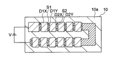
- the first upper electrode layer D1X is electrically connected to the negative electrode of the DC power source V
- the second lower electrode layer D2Y is electrically connected to the positive electrode of the DC power source V.
- the solid electrolyte integrated element shown in FIG. 3 has a structure in which all units including a plurality of (here, 12) solid electrolyte elements including the first and second solid electrolyte layers S1 and S2 are connected in series. .
- the configuration shown in FIG. 3 has an advantage that it can be routed as a circuit.
- units U1 and U2 in which a plurality of (here, five) solid electrolyte elements including the first and second solid electrolyte layers S1 and S2 are connected in series are connected in parallel.
- the structure shown in FIG. 4 has an advantage that even if there is a defect in one unit, a desired function can be exhibited by the other unit operating normally.
- a plurality (three) of units U3 to U in which a plurality of (here, two) solid electrolyte elements including the first and second solid electrolyte layers S1 and S2 are connected in parallel. It has a structure in which U5s are connected in series. Even when one solid electrolyte element in one unit is defective, there is an advantage that a desired function can be exhibited by the remaining solid electrolyte elements of the unit operating normally.
- the solid electrolyte integrated device 100 when the solid electrolyte integrated device 100 is applied to a device that allows gas to pass through the solid electrolyte layer as an anion, such as an oxygen concentrator, the first upper portion as in the examples of FIGS. 3 to 5.
- the electrode layer D1X is electrically connected to the negative electrode of the DC power source V
- the second lower electrode layer D2Y is electrically connected to the positive electrode of the DC power source V
- the oxygen becomes oxygen ions, passes through the solid electrolyte integrated device 100, and is concentrated in the space on the second main surface 10b side of the substrate 10. Thereby, the oxygen concentration in each space can be controlled.
- the solid electrolyte integrated element 100 when the solid electrolyte integrated element 100 is applied to a device that passes gas through a solid electrolyte layer as a cation, such as a hydrogen generator, the first upper electrode layer D1X is a positive electrode of the DC power source V.
- the second lower electrode layer D2Y is electrically connected to the negative electrode of the DC power source V, hydrogen in, for example, water vapor on the first main surface 10a side of the substrate 10 is solid electrolyte integrated.
- the element 100 is transmitted as protons so that hydrogen can be supplied into the space on the second main surface 10 b side of the substrate 10.
- the solid electrolyte integrated element 100 has a lower current value by electrically connecting a plurality of solid electrolyte layers including the first and second solid electrolyte layers S1 and S2 in series. A desired function can be exhibited.
- the first and second solid electrolyte layers S1 and S2 electrically connected in series of the solid electrolyte integrated device 100 according to the present embodiment are the first main surface 10a of the substrate 10 such as glass having a predetermined rigidity. Since it is provided on the top (first and second lower electrode layers D1Y and D2Y), the stress applied to the first and second solid electrolyte layers S1 and S2 can be reduced.
- the stress applied to the solid electrolyte layer can be reduced while connecting a plurality of solid electrolyte layers in series to reduce the current.
- the solid electrolyte integrated element 100 is not limited to the configuration shown in FIGS. 1 and 2 described above, but has a configuration as shown in Modifications 1 to 3 shown in FIGS. 6 to 11 below. May be.
- FIG. 6 is a cross-sectional view showing an example of the solid electrolyte integrated device 100 according to the first modification.
- FIG. 7 is a plan view of the substrate 10 of the solid electrolyte integrated device 100 shown in FIG. 6 as viewed from the first main surface 10a side.
- the cross section in FIG. 6 corresponds to the cross section along the line AA in FIG.
- a fifth through hole D1XP is provided in the same direction as the normal line N1 penetrating the first upper electrode layer D1X in the vertical direction and perpendicular to the first main surface 10a. You may be allowed to.
- the first and second through holes P1 and P2 of the substrate 10 have a rectangular (polygonal) cross section.
- FIG. 8 is a cross-sectional view showing an example of the solid electrolyte integrated device 100 according to the second modification.
- FIG. 9 is a plan view of the substrate 10 of the solid electrolyte integrated device 100 shown in FIG. 8 as viewed from the first main surface 10a side.
- the cross section in FIG. 8 corresponds to the cross section along the line AA in FIG.
- the first lower electrode layer D1Y is formed on the first main surface 10a so as to cover the entire first opening P1a on the first main surface 10a side of the first through hole P1. May be provided.
- the second lower electrode layer D2Y may be provided on the first main surface 10a so as to cover the entire second opening P2a on the first main surface 10a side of the second through hole P2.
- FIG. 10 is a cross-sectional view showing an example of the solid electrolyte integrated device 100 according to the third modification.
- FIG. 11 is a plan view of the configuration in the vicinity of the plane along the first main surface 10a of the substrate 10 of the solid electrolyte integrated device 100 shown in FIG. 10 as viewed from below.
- the cross section in FIG. 10 corresponds to the cross section along the line AA in FIG.
- the first upper electrode layer D1X extends on the first solid electrolyte layer S1 through which the normal line N1 perpendicular to the first main surface 10a passing through the first through hole P1 passes. You may be allowed to.
- the second upper electrode layer D2X may extend on the second solid electrolyte layer S2 through which the normal line N2 perpendicular to the first main surface 10a passing through the second through hole P2 passes.
- 12 to 16 are cross-sectional views showing an example of each process of the manufacturing method of the solid electrolyte integrated device 100 of the first modification shown in FIG.
- a substrate 10 having a first main surface 10a and a second main surface 10b opposite to the first main surface 10a and having an insulating surface is prepared (first step). ).
- the first lower electrode layer D1Y and the second lower electrode layer D2Y having conductivity are formed on the first main surface 10a of the substrate 10 (second step).
- the first lower electrode layer D1Y is formed on the first main surface 10a of the substrate 10 by printing a paste pattern containing metal ink on the first main surface 10a of the substrate 10 and baking the printed paste pattern.
- the second lower electrode layer D2Y can be selectively formed.
- the mask resist is selectively formed on the first main surface 10a of the substrate 10 for masking, and then a thin film containing metal is formed by sputtering, printing, etc., and then the mask resist is peeled off to form the substrate 10
- the first lower electrode layer D1Y and the second lower electrode layer D2Y can be selectively formed on the first main surface 10a of the substrate 10 by firing the thin film remaining on the first main surface 10a. it can.
- a first solid electrolyte layer S1 provided on the first lower electrode layer D1Y and electrically connected to the first lower electrode layer D1Y and having ion conductivity is formed.
- a second solid electrolyte layer S2 having ion conductivity and electrically connected to the second lower electrode layer D2Y is formed so as to be separated from the first solid electrolyte layer S1 (first 3 steps).
- the first solid electrolyte layer S1 and the second solid electrolyte layer S2 can be formed by selectively forming and baking a solid electrolyte by RF (Radio Frequency) sputtering using a lithography technique. .
- RF Radio Frequency
- a first upper electrode layer D1X is formed on the first major surface 10a side, spaced apart from the first lower electrode layer D1Y via the first solid electrolyte layer S1 (fourth step). ). Further, in the fourth step, the second upper electrode layer D2X is formed on the first main surface 10a side so as to be separated from the second lower electrode layer D2Y via the second solid electrolyte layer S2.
- a paste pattern containing a metal ink is printed on the first main surface 10a side with a separation from the first lower electrode layer D1Y via the first solid electrolyte layer S1, and the second pattern via the second solid electrolyte layer S2.
- Printing is performed on the first main surface 10a side apart from the lower electrode layer D2Y. Then, by firing the printed paste pattern, the first upper electrode layer D1X electrically connected to the first solid electrolyte layer S1 and the second electrically connected to the second solid electrolyte layer S2
- the upper electrode layer D2X can be selectively formed.
- a mask resist is selectively formed on the first main surface 10a side of the substrate 10 for masking, and then a thin film containing metal is formed by sputtering, printing, etc., and then the mask resist is peeled off to form the substrate 10
- the first lower electrode layer D1Y and the second lower electrode layer D2Y can be selectively formed on the first main surface 10a side of the substrate 10 also by baking the thin film remaining on the first main surface 10a side. it can.
- the first lower electrode layer D1Y and the second upper electrode layer D2X are electrically connected on the first main surface 10a side by the process shown in FIG.
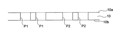
- the first through hole P ⁇ b> 1 and the second through hole P ⁇ b> 2 penetrating between the first main surface 10 a and the second main surface 10 b are formed from the second main surface 10 b side of the substrate 10.
- the first through-hole P1 and the second through-hole P2 can be formed by selectively etching the substrate 10 from the second main surface 10b side by reactive ion etching (RIE: Reactive Ion Etching). RIE: Reactive Ion Etching.
- the first through hole P1 is formed so that the first lower electrode layer D1Y covers a part of the first opening P1a on the first main surface 10a side of the first through hole P1.
- the second through hole P2 is formed such that the second lower electrode layer D2Y covers a part of the second opening P2a on the first main surface 10a side of the second through hole P2.
- a second additional electrode layer D2A electrically connected to the second lower electrode layer D2Y is formed in the vicinity of the second opening P2a in the second through hole P2 (sixth step).
- a paste pattern containing metal ink is printed from the second main surface 10b side in the vicinity of the first opening P1a in the first through hole P1 and in the vicinity of the second opening P2a in the second through hole P2.
- the printed paste pattern is fired.
- the first additional electrode layer D1A and the second additional electrode layer D2A can be selectively formed.
- the mask resist is selectively formed on the second main surface 10b side of the substrate 10 and masked, a thin film containing metal is formed by sputtering or printing, and then the mask resist is peeled off to form the first
- the thin film remaining in the vicinity of the first opening P1a in the through hole P1 and in the vicinity of the second opening P2a in the second through hole P2 may be fired.
- the first additional electrode layer D1A and the second additional electrode layer D2A can be selectively formed.
- the first and second solid electrolyte layers S1 and S2 are formed on the first main surface 10a (first and second lower electrode layers D1Y and D2Y) of the substrate 10 having a predetermined rigidity. Since it is formed (third step in FIG. 14), the mechanical stress applied to the first and second solid electrolyte layers S1 and S2 at the time of manufacture can be reduced.
- the through holes of the substrate are formed after forming the respective components of the solid electrolyte integrated element.
- the through holes of the substrate are formed in the solid electrolyte integrated element. It may be preliminarily formed before forming the respective components.
- 17 to 24 are cross-sectional views showing other examples of the respective steps of the method for manufacturing the solid electrolyte integrated element 100 of Modification 1 shown in FIG.
- the first main surface 10a and the second main surface 10b opposite to the first main surface 10a are provided in the same manner as the first step described above, and the surface is insulative.
- a substrate 10 is prepared.
- the first through hole P1 and the second through hole P2 penetrating between the first main surface 10a and the second main surface 10b are formed by, for example, reactive ion etching.
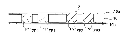
- a metal Z such as copper (temporary filler) is formed by, for example, plating so as to fill the first through hole P1 and the second through hole P2.
- the metal Z is also formed on the first main surface 10a and the second main surface 10b.
- the metal Z film on the first main surface 10a and the second main surface 10b of the substrate 10 is polished and removed by, for example, a CMP (Chemical Mechanical Polishing) method.
- CMP Chemical Mechanical Polishing
- the first main surface 10a of the substrate 10 (the first main surface 10a side of the metal Z in the first and second through holes P1 and P2) as in the second step described above.
- the first lower electrode layer D1Y and the second lower electrode layer D2Y having conductivity are formed on the surface including the first surface.
- the first solid electrolyte layer S1 provided on the first lower electrode layer D1Y and electrically connected to the first lower electrode layer D1Y, as in the third step described above.
- the second solid electrolyte layer S2 electrically connected to the second lower electrode layer D2Y is formed on the second lower electrode layer D2Y so as to be separated from the first solid electrolyte layer S1.
- the first solid is separated from the first lower electrode layer D1Y via the first solid electrolyte layer S1 and on the first main surface 10a side, as in the above-described fourth step.
- a first upper electrode layer D1X that is electrically connected to the electrolyte layer S1 and has conductivity is formed.
- the second upper electrode having electrical conductivity is electrically connected to the second solid electrolyte layer S2 on the first main surface 10a side and separated from the second lower electrode layer D2Y via the second solid electrolyte layer S2.
- Layer D2X is formed.
- the first lower electrode layer D1Y and the second upper electrode layer D2X are electrically connected on the first main surface 10a side.
- the first through hole P1 and the second through hole P2 penetrating between the first main surface 10a and the second main surface 10b are formed as in the fifth step described above.
- the second main surface 10b side of the substrate 10 is formed.
- the metal Z temporary filler
- the first lower electrode layer D1Y is electrically connected in the vicinity of the first opening P1a in the first through hole P1.
- the first additional electrode layer D1A thus formed is formed.
- a second additional electrode layer D2A electrically connected to the second lower electrode layer D2Y is formed in the vicinity of the second opening P2a in the second through hole P2.
- the solid electrolyte integrated element 100 according to Modification 1 shown in FIG. 6 can be manufactured.
- the solid electrolyte integrated element It is possible to exhibit the function of ion permeability.
- the lower electrode layer is an example of a solid electrolyte integrated element provided on the first main surface so as to border a part of the opening on the first main surface side of the through hole of the substrate. Will be described.
- FIG. 25 is a cross-sectional view showing an example of the solid electrolyte integrated device 100 according to the second embodiment.
- a case where there is one through-hole for one solid electrolyte layer (one unit) is shown.
- the same reference numerals as those in FIG. 1 indicate the same configurations as those in the first embodiment, and the description thereof is omitted.
- a solid electrolyte integrated element 100 in which a plurality of solid electrolyte layers (solid electrolyte layers) according to the second embodiment are integrated includes a substrate 10, a first lower electrode layer D1Y, 1 solid electrolyte layer S1, 1st upper electrode layer D1X, 2nd lower electrode layer D2Y, 2nd solid electrolyte layer S2, and 2nd upper electrode layer D2X are provided.
- the first and second additional electrode layers D1A and D2A are omitted as compared with the first embodiment.
- the first lower electrode layer D1Y is provided on the first main surface 10a so as to border a part of the first opening P1a on the first main surface 10a side of the first through hole P1.
- the second lower electrode layer D2Y is provided on the first main surface 10a so as to border a part of the second opening P2a on the first main surface 10a side of the second through hole P2.
- the solid electrolyte integrated device 100 electrically connects a plurality of solid electrolyte layers including the first and second solid electrolyte layers S1 and S2 in series.
- a desired function can be exhibited with a lower current value.
- the first and second solid electrolyte layers S1 and S2 electrically connected in series of the solid electrolyte integrated element 100 according to the second embodiment are the first main surface of the substrate 10 such as glass having a predetermined rigidity. 10a (first and second lower electrode layers D1Y and D2Y). For this reason, the stress applied to the first and second solid electrolyte layers S1 and S2 can be reduced.
- the stress applied to the solid electrolyte layer can be reduced while connecting a plurality of solid electrolyte layers in series to reduce the current.
- 26 to 30 are cross-sectional views showing an example of each step of the method for manufacturing the solid electrolyte integrated device 100 according to the second embodiment shown in FIG.
- the first main surface 10a and the second main surface 10b opposite to the first main surface 10a are provided, and the surface is insulative.
- a substrate 10 is prepared.
- the first main surface 10a of the substrate 10 (the first main surface 10a side of the metal Z in the first and second through holes P1, P2).
- the first lower electrode layer D1Y and the second lower electrode layer D2Y having conductivity are formed on the surface including the first surface.
- the first lower electrode layer D1Y is provided on the first lower electrode layer D1Y and is electrically connected to the first lower electrode layer D1Y and has ion conductivity.
- 1 Solid electrolyte layer S1 is formed.
- a second solid electrolyte layer S2 having ion conductivity and electrically connected to the second lower electrode layer D2Y is formed so as to be separated from the first solid electrolyte layer S1. .
- the first solid is separated from the first lower electrode layer D1Y via the first solid electrolyte layer S1 and on the first main surface 10a side.
- a first upper electrode layer D1X that is electrically connected to the electrolyte layer S1 and has conductivity is formed.
- the second upper electrode having electrical conductivity is electrically connected to the second solid electrolyte layer S2 on the first main surface 10a side and separated from the second lower electrode layer D2Y via the second solid electrolyte layer S2.
- Layer D2X is formed.
- first lower electrode layer D1Y and the second upper electrode layer D2X are electrically connected on the first main surface 10a side.
- the first through hole P ⁇ b> 1 and the second through hole P ⁇ b> 2 penetrating between the first main surface 10 a and the second main surface 10 b are formed as in the fifth step described above.
- the second main surface 10b side of the substrate 10 is formed.
- the first and second through holes P1 and P2 penetrating between the first main surface 10a and the second main surface 10b are formed, and the first lower electrode layer D1Y is continuously formed from the first through hole P1.
- a fourth through hole D2YP that penetrates the second lower electrode layer D2Y continuously from the third through hole D1YP and the second through hole P2 is formed from the second main surface 10b side of the substrate 10.
- the first lower electrode layer D1Y is opened to border the first opening P1a on the first main surface 10a side of the first through hole P1, and the second lower electrode layer D2Y is formed to the second through hole. It opens so that the 2nd opening part P2a by the side of the 1st main surface 10a of P2 may be bordered.
- the first through hole P1 and the second through hole P2 can be formed by selectively etching the substrate 10 from the second main surface 10b side by reactive ion etching. . Further, the first and second lower electrode layers D1Y and D2Y are selectively etched from the second main surface 10b side through the first through hole P1 and the second through hole P2 by reactive ion etching under different conditions. Thus, the third through hole D1YP and the fourth through hole D2YP can be formed.
- the solid electrolyte integrated device 100 according to the second embodiment shown in FIG. 25 can be manufactured.
- the third and fourth through holes D1YP and D2YP are formed in advance during or after the formation of the first and second lower electrode layers D1Y and D2Y (the step shown in FIG. 27), and then the third through holes D1YP are formed.
- the second through hole P2 may be formed from the second main surface 10b side of the substrate 10 so as to be continuously connected to the first through hole P1 and the fourth through hole D2YP so as to be continuously connected. .
- first and second solid electrolyte layers S1 and S2 and the first and second upper electrode layers D1X and D2X may be the same as those in the first embodiment and the first to third modifications.
Landscapes
- Chemical & Material Sciences (AREA)
- Chemical Kinetics & Catalysis (AREA)
- Electrochemistry (AREA)
- Engineering & Computer Science (AREA)
- Organic Chemistry (AREA)
- Materials Engineering (AREA)
- Metallurgy (AREA)
- General Physics & Mathematics (AREA)
- Inorganic Chemistry (AREA)
- Physics & Mathematics (AREA)
- Health & Medical Sciences (AREA)
- Life Sciences & Earth Sciences (AREA)
- Manufacturing & Machinery (AREA)
- General Chemical & Material Sciences (AREA)
- Condensed Matter Physics & Semiconductors (AREA)
- Molecular Biology (AREA)
- Analytical Chemistry (AREA)
- Biochemistry (AREA)
- General Health & Medical Sciences (AREA)
- Immunology (AREA)
- Pathology (AREA)
- Fuel Cell (AREA)
- Electrolytic Production Of Non-Metals, Compounds, Apparatuses Therefor (AREA)
Abstract
表面が絶縁性を有する基板を備えた固体電解質集積素子において、第1下部電極層と第2上部電極層とが、第1主面側で電気的に接続され、第1上部電極層、前記第1下部電極層、前記第2上部電極層、及び第2下部電極層は、いずれも、イオンを透過する又は/及びイオン酸化還元能を有するものであり、且つ、金属もしくは金属酸化物のいずれか、またはその両方を含むものであり、さらに通気する通気部を有するものである。
Description
本発明は、固体電解質集積素子、固体電解質集積素子の製造方法、及び、固体電解質素子に関する発明である。
従来、例えば、固体電解質素子は、酸素センサや酸素濃縮器などに用いられている。
そして、固体電解質素子の集積効率の向上と低電流化のために、複数の固体電解質素子を直列に接続して集積した固体電解質集積素子が提案されている(例えば、特許文献1ないし3参照)。
例えば、上記特許文献1では、固体電解質層に貫通孔を形成し、当該貫通孔を介して複数の電極を直列に接続する構造が開示されている。しかしながら、この構造においては、貫通孔が設けられた固体電解質層に応力がかかり、固体電解質集積素子が崩壊してしまう問題がある。
また、特許文献2では、複数の固体電解質素子を位置決め突起に固定し、直列に接合させる電気化学セルの構造が開示されている。これにより、各電気化学セル間に接続配線のためのクリアランスを設ける必要がなくなり、よって、コンパクト化が図れる。しかしながら、この特許文献2に記載の構造では、突起と固体電解質素子との接合の際に応力がかかり、固体電解質素子を破損する問題がある。
また、上記特許文献3では、ダミーのシリコン基板上に電極/固体電解質/電極を積層した積層体に上部基板を陽極接合し、ダミーのシリコン基板をウェットエッチングで除去し、次いで下部基板を陽極接合することにより、2枚の基板で固体電解質の薄膜(固体電解質層)を挟持した素子を製造する方法が開示されている。
しかしながら、この特許文献3に記載の構造では、固体電解質層に下部基板を接合する際に、固体電解質層に応力がかかるため、当該固体電解質層が損傷する問題がある。
しかしながら、この特許文献3に記載の構造では、固体電解質層に下部基板を接合する際に、固体電解質層に応力がかかるため、当該固体電解質層が損傷する問題がある。
上述のように、従来の固体電解質集積素子では、固体電解質層に応力が印加されて固体電解質集積素子が損傷し、崩壊する問題がある。
そこで、本発明では、低電流化しつつ、固体電解質層に印加される応力を低減することが可能な固体電解質集積素子を提供することを目的とする。
本発明の一態様に係る実施形態に従った固体電解質集積素子は、表面が絶縁性を有する基板を備えた固体電解質集積素子であって、基板はその一方の面側に、第1主面と、前記第1主面の裏面側に設けられた第2主面とを有し、前記第1主面と前記第2主面との間を貫通する第1、第2の2つの貫通孔が設けられており、前記固体電解質集積素子は、前記第1貫通孔の前記第1主面側における第1開口部の一部を被覆する又は縁どるように前記第1主面上に設けられた、導電性を有する第1下部電極層と、前記第1下部電極層上に電気的に接続された、第1固体電解質層と、前記第1主面側に設けられ、前記第1固体電解質層を介し、且つ前記第1下部電極層と離間し、前記第1固体電解質層と電気的に接続された第1上部電極層と、前記第2貫通孔の前記第1主面側における第2開口部の一部を被覆する又は縁どるように前記第1主面上に設けられた、導電性を有する第2下部電極層と、前記第2下部電極層上に、前記第1固体電解質層と離間して設けられ、且つ前記第2下部電極層に電気的に接続された第2固体電解質層と、前記第1主面側に設けられ、前記第2固体電解質層を介して前記第2下部電極層と離間し、且つ前記第2固体電解質層と電気的に接続された、第2上部電極層と、を備え、前記第1下部電極層と前記第2上部電極層とが、前記第1主面側で電気的に接続され、前記第1上部電極層、前記第1下部電極層、前記第2上部電極層、及び前記第2下部電極層は、いずれも、イオンを透過する又は/及びイオン酸化還元能を有するものであって、且つ、金属もしくは金属酸化物のいずれか、またはその両方を含むものであり、さらに通気する通気部を有するものである。
本発明の一態様に係る固体電解質集積素子、固体電解質集積素子の製造方法、及び、固体電解質素子は、固体電解質層に印加される機械的応力を低減することができる。
以下、本発明に係る実施形態について図面に基づいて説明する。
図1は、第1実施形態に係る固体電解質集積素子100の一例を示す断面図である。また、図2は、図1に示す固体電解質集積素子100の基板10の第1主面10aに沿った平面近傍の構成を下方から見た平面図である。なお、図1の断面は、図2のA-A線に沿った断面に対応する。
なお、各図面に基づいた説明においては、固体電解質集積素子100の基板10の位置を基準として、当該基板10の第2主面10bから第1主面10aへの向きを上方向とし、第1主面10aから第2主面10bへの向きを下方向としている。そして、当該基板10の第1主面10a側を上側(上方)とし、当該基板10の第2主面10b側を下側(下方)としている。
なお、各図面に基づいた説明においては、固体電解質集積素子100の基板10の位置を基準として、当該基板10の第2主面10bから第1主面10aへの向きを上方向とし、第1主面10aから第2主面10bへの向きを下方向としている。そして、当該基板10の第1主面10a側を上側(上方)とし、当該基板10の第2主面10b側を下側(下方)としている。
例えば、図1、図2に示すように、本実施形態に係る複数の固体電解質層(固体電解質の層)を集積させた固体電解質集積素子100は、基板10と、第1下部電極層D1Yと、第1固体電解質層S1と、第1上部電極層D1Xと、第1追加電極層D1Aと、第2下部電極層D2Yと、第2固体電解質層S2と、第2上部電極層D2Xと、第2追加電極層D2Aと、を備える。なお、固体電解質集積素子100の第1(第2)固体電解質層S1(S2)の位置を基準として、当該第1(第2)固体電解質層S1(S2)の上面に接続された電極を第1(第2)上部電極層D1X(D2X)とし、当該第1(第2)固体電解質層S1(S2)の下面に接続された電極を第1(第2)下部電極層D1Y(D2Y)としている。
この固体電解質集積素子100は、例えば、酸素濃縮器又は水素製造器に適用される。
なお、基板10と、第1下部電極層D1Yと、第1固体電解質層S1と、第1上部電極層D1Xとにより、1個の固体電解質素子が構成される。そして、このような固体電解質素子が電気的に複数個直列(図1の例では最小単位の2個に注目して図示している)に接続されることで、上記固体電解質集積素子100が構成される。
以下、固体電解質集積素子100の各構成について説明する。
以下、固体電解質集積素子100の各構成について説明する。
(基板10)
ここで、例えば、図1、図2に示すように、基板10は、一方の面に第1主面10aと、この第1主面10aの裏面側の第2主面10bとを有する。この基板10は、第1主面10aと第2主面10bとの間を貫通する第1貫通孔P1及び第2貫通孔P2が設けられている。この基板10の第1貫通孔P1及び第2貫通孔P2は、第1主面10aと第2主面10bとの間で気体を通気可能にするものである。
ここで、例えば、図1、図2に示すように、基板10は、一方の面に第1主面10aと、この第1主面10aの裏面側の第2主面10bとを有する。この基板10は、第1主面10aと第2主面10bとの間を貫通する第1貫通孔P1及び第2貫通孔P2が設けられている。この基板10の第1貫通孔P1及び第2貫通孔P2は、第1主面10aと第2主面10bとの間で気体を通気可能にするものである。
さらに、基板10は、表面が絶縁性を有する。例えば、基板10は、ガラスで構成されている。また、基板10は、シリコン酸化物を外表面に備えたシリコン基板であってもよい。
ここで、基板10の外表面とは、基板10の第1、第2主面10a、10bおよび側面を含む概念である。当該基板10自体に電流が流れないように、基板10は外表面に絶縁性を有する。
ここで、基板10の外表面とは、基板10の第1、第2主面10a、10bおよび側面を含む概念である。当該基板10自体に電流が流れないように、基板10は外表面に絶縁性を有する。
より詳しくは、この基板10の材料としては、耐熱性や電気絶縁性に優れるものとして、ガラス、酸化物が被覆されたシリコン、酸化物被覆金属(Ti、Niや合金系)、酸化物セラミックス(Al2O3、ジルコニア、マグネシア、ランタンクロマイト系など)が選択されてもよい。
そして、開口加工が容易な材料として、より好ましくは、ガラス、酸化物が被覆されたシリコンが選択される。
また、材料価格および製造コストにおいて優位な材料として、より好ましくは、酸化物が被覆されたシリコンが選択される。
そして、開口加工が容易な材料として、より好ましくは、ガラス、酸化物が被覆されたシリコンが選択される。
また、材料価格および製造コストにおいて優位な材料として、より好ましくは、酸化物が被覆されたシリコンが選択される。
なお、図1、図2の例では、第1貫通孔P1及び第2貫通孔P2がそれぞれ4個の場合を示しているが、第1貫通孔P1及び第2貫通孔P2がそれぞれ1個ないし3個、又は、5個以上であってもよい。
また、この基板10は、その上部に形成する各層を支持する点と、貫通孔を容易に形成できる点から、その厚さが、例えば、50μm~3000μmの範囲であるのが好ましい。
そして、基板10の第1及び第2貫通孔P1、P2は、例えば、第1主面の側から見て円形の形状を有する。この場合、この第1及び第2貫通孔P1、P2の円形の形状の直径は、例えば、0.01mm~30mmの範囲である。
なお、基板10の第1及び第2貫通孔P1、P2は、例えば、第1主面の側から見て、円形以外の長方形や、六角形等の多角形の形状を有していてもよい。
なお、基板10の第1及び第2貫通孔P1、P2は、例えば、第1主面の側から見て、円形以外の長方形や、六角形等の多角形の形状を有していてもよい。
(第1下部電極層D1Y)
また、第1下部電極層D1Yは、例えば、図1に示すように、第1貫通孔P1の第1主面10a側における第1開口部P1aの一部を被覆するように第1主面10a上に設けられている。この第1下部電極層D1Yが第1開口部P1aの一部を被覆することで、第1開口部P1aの電位を所定値に制御することができるようになっている。
また、第1下部電極層D1Yは、例えば、図1に示すように、第1貫通孔P1の第1主面10a側における第1開口部P1aの一部を被覆するように第1主面10a上に設けられている。この第1下部電極層D1Yが第1開口部P1aの一部を被覆することで、第1開口部P1aの電位を所定値に制御することができるようになっている。
この第1下部電極層D1Yは、導電性を有する。特に、この第1下部電極層D1Yは、イオンを透過し又は/及びイオン酸化還元能を有する。
なお、後述の第2実施形態のように、第1下部電極層D1Yは、第1貫通孔P1の第1主面10a側における第1開口部P1aの一部を縁どるように第1主面10a上に設けられていてもよい。
この第1下部電極層D1Yには、例えば、図1に示すように、当該第1下部電極層D1Yを上下方向に貫通し且つ基板10の第1貫通孔P1に連通する第3貫通孔D1YPが設けられている。
そして、この第1下部電極層D1Yの第3貫通孔D1YP内には、第1固体電解質層S1の一部S1Pが充填されている。これにより、第1固体電解質層S1自体の抵抗値を下げるとともに、この第1固体電解質層S1と第1下部電極層D1Yとの間の電気的な接触抵抗を低減することができる。
そして、この第1下部電極層D1Yの第3貫通孔D1YP内には、第1固体電解質層S1の一部S1Pが充填されている。これにより、第1固体電解質層S1自体の抵抗値を下げるとともに、この第1固体電解質層S1と第1下部電極層D1Yとの間の電気的な接触抵抗を低減することができる。
また、この第1下部電極層D1Yは、例えば、金属もしくは金属酸化物のいずれか、またはその両方を含むものであり、通気する通気部(図示せず)を有していてもよい。この通気部は、例えば、第1下部電極層D1Yの第1貫通孔P1側の気体が第1固体電解質層S1との界面まで通気可能な形状を有する。この通気部は、例えば、メッシュ状又は多孔質の形状であってもよい。
そして、この第1下部電極層D1Yは、厚さが0.01~1000μmの範囲であることが好ましい。
(第1固体電解質層S1)
また、第1固体電解質層S1は、例えば、図1に示すように、第1下部電極層D1Y上に設けられている。そして、この第1固体電解質層S1は、第1下部電極層D1Yに電気的に接続されている。なお、この第1固体電解質層S1と第1下部電極層D1Yとの間にイオン伝導性を有する中間層(図示せず)が設けられていてもよい。
また、第1固体電解質層S1は、例えば、図1に示すように、第1下部電極層D1Y上に設けられている。そして、この第1固体電解質層S1は、第1下部電極層D1Yに電気的に接続されている。なお、この第1固体電解質層S1と第1下部電極層D1Yとの間にイオン伝導性を有する中間層(図示せず)が設けられていてもよい。
特に、第1固体電解質層S1は、第1下部電極層D1Yの上面D1Yaから側面D1Ybの一部に亘って被覆している。これにより、第1固体電解質層S1と第1下部電極層D1Yとの間の接触抵抗が低減されるようになっている。
さらに、第1固体電解質層S1は、その側面S1Xの一部が第1上部電極層D1Xにより被覆されている。特に、第1上部電極層D1Xは、例えば、図1に示すように、第1固体電解質層S1の上面S1aから側面S1Xの一部に亘って被覆している。これにより、この第1固体電解質層S1は、第1上部電極層D1Xに電気的に接続され、第1固体電解質層S1と第1上部電極層D1Xとの間の接触抵抗が低減されるようになっている。なお、この第1固体電解質層S1と第1上部電極層D1Xとの間に電子-イオン伝導性を有する中間層(図示せず)が設けられていてもよい。
また、この第1固体電解質層S1は、イオン伝導性し、例えば、プロトン伝導性、炭酸イオン伝導性、又は、酸化物イオン伝導性を有する。特に、固体電解質集積素子100が酸素濃縮器に適用される場合には、第1固体電解質層S1は、酸化物イオン伝導性を有する。この場合、第1固体電解質層S1は、例えば、600°の雰囲気で、1.0×10⁻³S/cmの酸化物イオン伝導性を有する。
また、第1固体電解質層S1は、第1下部電極層D1Y上における厚さが0.05μm~300μmの範囲であることが好ましい。
(第1上部電極層D1X)
また、第1上部電極層D1Xは、第1固体電解質層S1を介して第1下部電極層D1Yと離間して第1主面10a側に設けられている。この第1上部電極層D1Xは、第1固体電解質層S1と電気的に接続され、導電性を有する。
また、第1上部電極層D1Xは、第1固体電解質層S1を介して第1下部電極層D1Yと離間して第1主面10a側に設けられている。この第1上部電極層D1Xは、第1固体電解質層S1と電気的に接続され、導電性を有する。
この第1上部電極層D1Xは、イオンを透過し又は/及びイオン酸化還元能を有する。
なお、この第1上部電極層D1Xは、例えば、金属もしくは金属酸化物のいずれか、またはその両方を含むものであり、通気する通気部(図示せず)を有していてもよい。この通気部は、例えば、第1上部電極層D1Xの表面の気体が第1固体電解質層S1との界面まで通気可能な形状を有する。この通気部は、例えば、メッシュ状又は多孔質の形状であってもよい。
そして、この第1上部電極層D1Xは、第1固体電解質層S1上におけるその厚さが0.01μm~300μmの範囲であることが好ましい。
(第1追加電極層D1A:任意層)
また、第1追加電極層D1Aは、例えば、図1に示すように、第1貫通孔P1内の第1開口部P1aの近傍に設けられ、且つ第1下部電極層D1Yと電気的に接続されている。この第1追加電極層D1Aにより、当該第1追加電極層D1Aに電気的に接続されている第1下部電極層D1Yを含めた抵抗値を下げるとともに、第1固体電解質層S1との間の電気的な接触抵抗を低減することができる。
また、第1追加電極層D1Aは、例えば、図1に示すように、第1貫通孔P1内の第1開口部P1aの近傍に設けられ、且つ第1下部電極層D1Yと電気的に接続されている。この第1追加電極層D1Aにより、当該第1追加電極層D1Aに電気的に接続されている第1下部電極層D1Yを含めた抵抗値を下げるとともに、第1固体電解質層S1との間の電気的な接触抵抗を低減することができる。
この第1追加電極層D1Aは、厚さが0.01μm~300μmの範囲であることが好ましい。
なお、この第1追加電極層D1Aは設けられなくともよい。この場合、第1下部電極層D1Yの表面が第1貫通孔P1側に露出する状態になる。
(第2下部電極層D2Y)
また、第2下部電極層D2Yは、第2貫通孔P2の第1主面10a側における第2開口部P2aの一部を被覆するように第1主面10a上に設けられている。この第2下部電極層D2Yが第2開口部P2aの一部を被覆することで、第2開口部P2aの電位を所定値に制御することができる。
また、第2下部電極層D2Yは、第2貫通孔P2の第1主面10a側における第2開口部P2aの一部を被覆するように第1主面10a上に設けられている。この第2下部電極層D2Yが第2開口部P2aの一部を被覆することで、第2開口部P2aの電位を所定値に制御することができる。
そして、この第2下部電極層D2Yは、導電性を有する。特に、この第2下部電極層D2Yは、イオンを透過し又は/及びイオン酸化還元能を有する。
なお、後述の第2実施形態のように、第2下部電極層D2Yは、第2貫通孔P2の第1主面10a側における第2開口部P2aの一部を縁どるように第1主面10a上に設けられていてもよい。
この第2下部電極層D2Yには、例えば、図1に示すように、当該第2下部電極層D2Yを上下方向に貫通し且つ基板10の第2貫通孔P2に連通する第4貫通孔D2YPが設けられている。
さらに、この第2下部電極層D2Yの第4貫通孔D2YP内には、第2固体電解質層S2の一部S2Pが充填されている。これにより、第2固体電解質層S2自体の抵抗値を下げるとともに、この第2固体電解質層S2と第2下部電極層D2Yとの間の接触抵抗を低減することができる。
さらに、この第2下部電極層D2Yの第4貫通孔D2YP内には、第2固体電解質層S2の一部S2Pが充填されている。これにより、第2固体電解質層S2自体の抵抗値を下げるとともに、この第2固体電解質層S2と第2下部電極層D2Yとの間の接触抵抗を低減することができる。
また、この第2下部電極層D2Yは、既述の第1下部電極層D1Yと同様の構成を有し、例えば、金属もしくは金属酸化物のいずれか、またはその両方を含むものであり、通気する通気部(図示せず)を有していてもよい。
そして、この第2下部電極層D2Yは、厚さが0.01~1000μmの範囲であることが好ましい。
なお、この第2下部電極層D2Y及び既述の第1下部電極層D1Yに適用できる電極材料としては、電気伝導性を有する材料であれば特に制限なく使用することができ、例えば、Pt、Pd、Ag、Au、W、Mo、Ta、Nb、Ni等の金属、及びそれら金属含む合金、ステンレス等の金属系の電子伝導体材料、ランタンストロンチウムコバルトフェライト(LSCF)、バリウムフェライト系、酸化コバルトマンガン、ランタンニッケレート等のセラミック系の酸素-電子混合伝導体、ITOやFTO等のスズ酸化物系やAZOやGZO等の亜鉛酸化物系である透明電極材料、これら材料の混合物や担持物、上記した固体電解質と混合したサーメットなどが挙げられるがこれらに限定されるものではない。
(第2固体電解質層S2)
また、第2固体電解質層S2は、例えば、図1に示すように、第2下部電極層D2Y上に、既述の第1固体電解質層S1と離間する(電気的に直接接続されない)ように、設けられている。そして、この第2固体電解質層S2は、第2下部電極層D2Yに電気的に接続されている。なお、この第2固体電解質層S2と第2下部電極層D2Yとの間に電子-イオン伝導性を有する中間層(図示せず)が設けられていてもよい。
また、第2固体電解質層S2は、例えば、図1に示すように、第2下部電極層D2Y上に、既述の第1固体電解質層S1と離間する(電気的に直接接続されない)ように、設けられている。そして、この第2固体電解質層S2は、第2下部電極層D2Yに電気的に接続されている。なお、この第2固体電解質層S2と第2下部電極層D2Yとの間に電子-イオン伝導性を有する中間層(図示せず)が設けられていてもよい。
特に、第2固体電解質層S2は、第2下部電極層D2Yの上面D2Yaから側面D2Ybの一部に亘って被覆している。これにより、第2固体電解質層S2と第2下部電極層D2Yとの間の接触抵抗が低減されるようになっている。
さらに、第2固体電解質層S2は、その側面S2Xの一部が第2上部電極層D2Xに被覆されている。特に、第2上部電極層D2Xは、例えば、図1に示すように、第2固体電解質層S2の上面S2aから側面S2Xの一部に亘って被覆している。これにより、この第2固体電解質層S2は、第2上部電極層D2Xに電気的に接続されており、このような構成により、第2固体電解質層S2と第1上部電極層D2Xとの間の接触抵抗が低減されるようになっている。なお、この第2固体電解質層S2と第2上部電極層D2Xとの間にイオン伝導性を有する中間層(図示せず)が設けられていてもよい。
この第2固体電解質層S2は、イオン伝導性を有し、例えば、プロトン伝導性、炭酸イオン伝導性、又は、酸化物イオン伝導性を有する。特に、固体電解質集積素子100が酸素濃縮器に適用される場合には、第2固体電解質層S2は、酸化物イオン伝導性を有する。この場合、第2固体電解質層S2は、第1固体電解質層S1と同様の酸化物イオン伝導性を有する。
また、第2固体電解質層S2は、第2下部電極層D2Y上における厚さが0.05μm~300μmの範囲であることが好ましい。
なお、この第2固体電解質層S2及び既述の第1固体電解質層S1に適用される固体電解質としては、酸化物イオン伝導体またはプロトン伝導体として知られている無機固体電解質を使用することができる。
例えば、酸化物イオン伝導体として知られる無機固体電解質としては、ランタンシリケートやセリウムシリケート等の(RE2O3)x(SiO2)6(REはLa,Ce,Pr,Nd,Smから選択される元素であり、xは3.5<x<6の条件を満たす。)で表されるアパタイト結晶構造を有する複合酸化物、Y2O3、Sc2O3、Yb2O3等により安定化された安定化ジルコニア、LaGaO3の基本組成を有するペロブスカイト構造を有しているGa系酸化物(ランタンガレート系酸化物)、ガドリニウム固溶セリア(ガドリアドープセリア)やサマリウム固溶セリア(サマリアドープセリア)等の希土類元素を固溶したセリウム酸化物等が挙げられるがこれらに限定されるものではない。また、上記した酸化物イオン伝導体は、1種単独の化合物としてもよいし、複数の化合物が任意に混合された複合酸化物としてもよい。また、固体電解質層は、単層として用いる他、多層体として用いてもよい。
また、プロトン伝導体として知られている無機固体電解質としては、酸化バリウムセリア(BaCeO3)、酸化ストロンチウムセリア(SrCeO3)、酸化ストロンチウムジルコニア(SrZrO3)、酸化カルシウムジルコニア(CaZrO3)、酸化ストロンチウムチタニア(SrTiO3)などの複合酸化物、ランタン-タングステン系複合酸化物等が挙げられるがこれらに限定されるものではない。また、上記したプロトンイオン伝導体は1種単独で用いてもよいし、任意に混合して用いてもよい。
(第2上部電極層D2X)
また、第2上部電極層D2Xは、第2固体電解質層S2を介して第2下部電極層D2Yと離間して第1主面10a側に設けられている。この第2上部電極層D2Xは、第2固体電解質層S2と電気的に接続され、導電性を有する。
また、第2上部電極層D2Xは、第2固体電解質層S2を介して第2下部電極層D2Yと離間して第1主面10a側に設けられている。この第2上部電極層D2Xは、第2固体電解質層S2と電気的に接続され、導電性を有する。
この第2上部電極層D2Xは、イオンを透過し又は/及びイオン酸化還元能を有する。
なお、この第2上部電極層D2Xは、例えば、金属もしくは金属酸化物のいずれか、またはその両方を含むものであり、通気する通気部(図示せず)を有していてもよい。この通気部は、例えば、第2上部電極層D2Xの表面の気体が第2固体電解質層S2との界面まで通気可能な形状を有する。この通気部は、例えば、メッシュ状又は多孔質の形状であってもよい。
そして、この第2上部電極層D2Xは、第2固体電解質層S2上におけるその厚さが0.01μm~300μmの範囲であることが好ましい。
なお、この第2上部電極層D2X及び既述の第1上部電極層D1Xに適用できる電極材料としては、電気伝導性を有する材料であれば特に制限なく使用することができ、例えば、Pt、Pd、Ag、Au、W、Mo、Ta、Nb、Ni等の金属、及びそれら金属含む合金、ステンレス等の金属系の電子伝導体材料、ランタンストロンチウムコバルトフェライト(LSCF)、バリウムフェライト系、酸化コバルトマンガン、ランタンニッケレート等のセラミック系の酸素-電子混合伝導体、ITOやFTO等のスズ酸化物系やAZOやGZO等の亜鉛酸化物系である透明電極材料、これら材料の混合物や担持物、上記した固体電解質と混合したサーメットなどが挙げられるがこれらに限定されるものではない。
(第2追加電極層D2A:任意層)
また、第2追加電極層D2Aは、例えば、図1に示すように、第2貫通孔P2内の第2開口部P2aの近傍に設けられ、且つ第2下部電極層D2Yと電気的に接続されている。この第2追加電極層D2Aにより、当該第2追加電極層D2Aに電気的に接続されている第2下部電極層D2Yを含めた抵抗値を下げるとともに、第2固体電解質層S2との間の電気的な接触抵抗を低減することができる。
また、第2追加電極層D2Aは、例えば、図1に示すように、第2貫通孔P2内の第2開口部P2aの近傍に設けられ、且つ第2下部電極層D2Yと電気的に接続されている。この第2追加電極層D2Aにより、当該第2追加電極層D2Aに電気的に接続されている第2下部電極層D2Yを含めた抵抗値を下げるとともに、第2固体電解質層S2との間の電気的な接触抵抗を低減することができる。
この第2追加電極層D2Aは、厚さが0.01μm~300μmの範囲であることが好ましい。
なお、この第2追加電極層D2Aは、省略されていてもよい。この場合、第2下部電極層D2Yの表面が第2貫通孔P2側に露出する状態になる。
なお、この第2追加電極層D2A及び既述の第1追加電極層D1Aは、既述の電極材料のうち、触媒能(酸素吸着能、解離作用等)に優れたものを使用することができ、具体的には、Pt、Pd、Ag、Ni等の金属や、ランタンストロンチウムコバルトフェライト(LSCF)、バリウムフェライト系、酸化コバルトマンガン、ランタンニッケレート等のセラミック系の酸素-電子混合伝導体、これら材料の混合物や担持物、上記した固体電解質と混合したサーメットなどが挙げられる。
(直列接続の構造)
ここで、既述の第1固体電解質層S1と第2固体電解質層S2とが直列に接続される部分の構成に注目して、説明する。
ここで、既述の第1固体電解質層S1と第2固体電解質層S2とが直列に接続される部分の構成に注目して、説明する。
例えば、図1、図2に示すように、第1下部電極層D1Yは、第1固体電解質層S1に被覆された第1領域E1と、第1固体電解質層S1に被覆されていない第2領域E2と、を有する。
そして、第1下部電極層D1Yの第2領域E2の一部が、第2上部電極層D2Xにより被覆されている。これにより、この第1下部電極層D1Yが、第2上部電極層D2Xに電気的接続されている。
さらに、第2固体電解質層S2は、その側面S2Xの一部が第2上部電極層D2Xに被覆されている。特に、第2上部電極層D2Xは、例えば、図1に示すように、第2固体電解質層S2の上面S2aから側面S2Xの一部に亘って被覆している。より詳しくは、第2上部電極層D2Xは、第2固体電解質層S2の一端上から第1下部電極層D1Yの一端上に亘って延在している。
上記直列接続の構造により、この第2固体電解質層S2は、第2下部電極層D2Yに電気的に接続されている。
すなわち、上述のような構造により、第1下部電極層D1Yと第2上部電極層D2Xとが、第1主面10a側で電気的に接続されている。すなわち、第1固体電解質層S1と第2固体電解質層S2とは、第1下部電極層D1Y及び第2上部電極層D2Xを介して、電気的に直列に接続されている。
なお、第1上部電極層D1Xは、第1電位に接続され第2下部電極層D2Yは、第1電位と異なる第2電位に接続される。より具体的には、第1上部電極層D1Xが直流電源の正極又は負極の何れか一方に電気的に接続され、第2下部電極層D2Yが直流電源の正極又は負極の残りの他方に電気的に接続される。
ここで、直列接続の具体例として、固体電解質集積素子100に、直流電源Vを接続する場合について説明する。図3は、複数の固体電解質集積素子を直列に接続した固体電解質集積素子の構成の一例を示す平面図である。また、図4は、複数の固体電解質集積素子を直列に接続した固体電解質集積素子の構成の他の例を示す平面図である。また、図5は、複数の固体電解質集積素子を直列に接続した固体電解質集積素子の構成のさらに他の例を示す平面図である。
この図3ないし図5の例では、第1上部電極層D1Xが直流電源Vの負極に電気的に接続され、第2下部電極層D2Yが直流電源Vの正極に電気的に接続されている。
そして、例えば、図3に示す固体電解質集積素子では、第1、第2固体電解質層S1、S2を含む複数(ここでは12個)の固体電解質素子からなるユニットが全て直列接続された構造を有する。この図3に示す構成は、回路として引き回しできる利点がある。
また、図4に示す固体電解質集積素子では、第1、第2固体電解質層S1、S2を含む複数(ここでは5個)の固体電解質素子が直列に接続されたユニットU1、U2が並列接続された構造を有する。この図4に示す構造は、一方のユニット内に欠陥がある場合にも、他方のユニットが正常に動作することで、所望の機能を発揮することができる利点がある。
また、図5に示す固体電解質集積素子では、第1、第2固体電解質層S1、S2を含む複数(ここでは2個)の固体電解質素子が並列接続された複数(3個)のユニットU3~U5同士を直列接続した構造を有する。1個のユニット内の一方の固体電解質素子に欠陥がある場合も、当該ユニットの残りの固体電解質素子が正常に動作することで、所望の機能を発揮することができる利点がある。
ここで、例えば、固体電解質集積素子100が酸素濃縮器のように、ガスを陰イオンとして固体電解質層内を通過させる装置に適用される場合、図3ないし図5の例のように第1上部電極層D1Xが直流電源Vの負極に電気的に接続され、第2下部電極層D2Yが直流電源Vの正極に電気的に接続されているときには、基板10の第1主面10a側の空間内の酸素が酸素イオンとなって、固体電解質集積素子100を透過し、基板10の第2主面10b側の空間内に酸素が濃縮されるようになっている。これにより、各空間内の酸素濃度を制御することができる。
また、例えば、固体電解質集積素子100が水素製造器のように、ガスを陽イオンとして固体電解質層内を通過させる装置に適用される場合には、第1上部電極層D1Xが直流電源Vの正極に電気的に接続され、第2下部電極層D2Yが直流電源Vの負極に電気的に接続されているときには、基板10の第1主面10a側の、例えば水蒸気中の水素が、固体電解質集積素子100をプロトンとして透過し、基板10の第2主面10b側の空間内に水素を供給できるようになっている。
このような本実施形態に係る固体電解質集積素子100は、第1、第2固体電解質層S1、S2を含む複数の固体電解質層を直列に電気的に接続することにより、より低い電流値で、所望の機能を発揮することができる。
そして、本実施形態に係る固体電解質集積素子100の直列に電気的に接続された第1、第2固体電解質層S1、S2は、所定の剛性を有するガラス等の基板10の第1主面10a上(第1、第2下部電極層D1Y、D2Y)に設けられているため、第1、第2固体電解質層S1、S2に印加される応力を低減することができる。
すなわち、本実施形態に係る固体電解質集積素子によれば、複数の固体電解質層を直列に接続して低電流化しつつ、固体電解質層に印加される応力を低減することができる。
ここで、固体電解質集積素子100は、既述の図1、図2に示す構成に限定されるものではなく、以下の図6ないし図11に示す変形例1ないし3に示すような構成であってもよい。
(変形例1)
図6は、変形例1に係る固体電解質集積素子100の一例を示す断面図である。また、図7は、図6に示す固体電解質集積素子100の基板10を第1主面10a側から見た平面図である。なお、図6の断面は、図7のA-A線に沿った断面に対応する。
図6は、変形例1に係る固体電解質集積素子100の一例を示す断面図である。また、図7は、図6に示す固体電解質集積素子100の基板10を第1主面10a側から見た平面図である。なお、図6の断面は、図7のA-A線に沿った断面に対応する。
この図6、図7に示すように、第1上部電極層D1Xを、上下方向に貫通し且つ第1主面10aに垂直な法線N1と同一の方向に第5の貫通孔D1XPが設けられているようにしてもよい。
同様に、第2上部電極層D2Xには、上下方向に貫通し且つ第2下部電極層D2Yの第4貫通孔D2YPを通る第1主面10aに垂直な法線N2が通る第6の貫通孔D2XPが設けられているようにしてもよい。
なお、この変形例1では、基板10の第1及び第2貫通孔P1、P2は、その断面が長方形(多角形)の形状を有している。
この変形例1に係る固体電解質集積素子100のその他の構成は、第1実施形態と同様である。
(変形例2)
図8は、変形例2に係る固体電解質集積素子100の一例を示す断面図である。また、図9は、図8に示す固体電解質集積素子100の基板10を第1主面10aの側から見た平面図である。なお、図8の断面は、図9のA-A線に沿った断面に対応する。
図8は、変形例2に係る固体電解質集積素子100の一例を示す断面図である。また、図9は、図8に示す固体電解質集積素子100の基板10を第1主面10aの側から見た平面図である。なお、図8の断面は、図9のA-A線に沿った断面に対応する。
この図8、図9に示すように、第1下部電極層D1Yは、第1貫通孔P1の第1主面10a側における第1開口部P1aの全体を被覆するように第1主面10a上に設けられていてもよい。
同様に、第2下部電極層D2Yは、第2貫通孔P2の第1主面10a側における第2開口部P2aの全体を被覆するように第1主面10a上に設けられていてもよい。
この変形例2に係る固体電解質集積素子100のその他の構成は、第1実施形態と同様である。
(変形例3)
図10は、変形例3に係る固体電解質集積素子100の一例を示す断面図である。また、図11は、図10に示す固体電解質集積素子100の基板10の第1主面10aに沿った平面近傍の構成を下方から見た平面図である。なお、図10の断面は、図11のA-A線に沿った断面に対応する。
図10は、変形例3に係る固体電解質集積素子100の一例を示す断面図である。また、図11は、図10に示す固体電解質集積素子100の基板10の第1主面10aに沿った平面近傍の構成を下方から見た平面図である。なお、図10の断面は、図11のA-A線に沿った断面に対応する。
この図10、図11に示すように、第1上部電極層D1Xは、第1貫通孔P1を通る第1主面10aに垂直な法線N1が通る第1固体電解質層S1上に延在しているようにしてもよい。
同様に、第2上部電極層D2Xは、第2貫通孔P2を通る第1主面10aに垂直な法線N2が通る第2固体電解質層S2上に延在しているようにしてもよい。
この変形例3に係る固体電解質集積素子100のその他の構成は、第1実施形態と同様である。
次に、以上のような構成を有する複数の固体電解質層を集積させた固体電解質集積素子100の製造方法について、既述の図6に示す変形例1の構成を一例として、説明する。なお、第1実施形態、他の変形例についても同様に説明される。
図12ないし図16は、図6に示す変形例1の固体電解質集積素子100の製造方法の各工程の一例を示す断面図である。
先ず、図12に示すように、第1主面10aと、第1主面10aと反対側の第2主面10bとを有し、表面が絶縁性を有する基板10を準備する(第1工程)。
次に、図13に示すように、基板10の第1主面10a上に、導電性を有する第1下部電極層D1Y及び第2下部電極層D2Yを形成する(第2工程)。
例えば、メタルインクを含むペーストパターンを基板10の第1主面10a上に印刷し、当該印刷されたペーストパターンを焼成することにより、基板10の第1主面10a上に第1下部電極層D1Y及び第2下部電極層D2Yを選択的に形成することができる。
なお、マスクレジストを基板10の第1主面10a上に選択的に形成してマスキングした後、スパッタや印刷等によりメタルを含有する薄膜を形成し、その後、マスクレジストを剥離して、基板10の第1主面10a上に残存する当該薄膜を焼成することによっても、基板10の第1主面10a上に第1下部電極層D1Y及び第2下部電極層D2Yを選択的に形成することができる。
次に、図14に示すように、第1下部電極層D1Y上に設けられ、第1下部電極層D1Yに電気的に接続され、イオン伝導性を有する第1固体電解質層S1を形成するとともに、第2下部電極層D2Y上に、第1固体電解質層S1と離間するように、第2下部電極層D2Yに電気的に接続され、イオン伝導性を有する第2固体電解質層S2を形成する(第3工程)。
例えば、リソグラフィ技術を用いて、RF(Radio Frequency)スパッタにより、固体電解質を選択的に成膜し、焼成することで、第1固体電解質層S1及び第2固体電解質層S2を形成することができる。
次に、図15に示すように、第1固体電解質層S1を介して第1下部電極層D1Yと離間して第1主面10a側に、第1上部電極層D1Xを形成する(第4工程)。
さらに、この第4工程において、第2固体電解質層S2を介して第2下部電極層D2Yと離間して第1主面10a側に、第2上部電極層D2Xを形成する。
さらに、この第4工程において、第2固体電解質層S2を介して第2下部電極層D2Yと離間して第1主面10a側に、第2上部電極層D2Xを形成する。
例えば、メタルインクを含むペーストパターンを、第1固体電解質層S1を介して第1下部電極層D1Yと離間して第1主面10a側に印刷するとともに第2固体電解質層S2を介して第2下部電極層D2Yと離間して第1主面10a側に印刷する。
そして、当該印刷されたペーストパターンを焼成することにより、第1固体電解質層S1と電気的に接続された第1上部電極層D1X、及び第2固体電解質層S2と電気的に接続された第2上部電極層D2Xを選択的に形成することができる。
そして、当該印刷されたペーストパターンを焼成することにより、第1固体電解質層S1と電気的に接続された第1上部電極層D1X、及び第2固体電解質層S2と電気的に接続された第2上部電極層D2Xを選択的に形成することができる。
なお、マスクレジストを基板10の第1主面10a側に選択的に形成してマスキングした後、スパッタや印刷等によりメタルを含有する薄膜を形成し、その後、マスクレジストを剥離して、基板10の第1主面10a側に残存する当該薄膜を焼成することによっても、基板10の第1主面10a側に第1下部電極層D1Y及び第2下部電極層D2Yを選択的に形成することができる。
なお、この図15に示す工程により、第1下部電極層D1Yと第2上部電極層D2Xとが、第1主面10a側で電気的に接続されることとなる。
次に、図16に示すように、第1主面10aと第2主面10bとの間を貫通する第1貫通孔P1及び第2貫通孔P2を、基板10の第2主面10b側から形成する(第5の工程)。
例えば、反応性イオンエッチング(RIE:Reactive Ion Etching)により、第2主面10b側から基板10を選択的にエッチングすることにより、第1貫通孔P1及び第2貫通孔P2を形成することができる。
特に、第1貫通孔P1は、第1下部電極層D1Yが第1貫通孔P1の第1主面10a側の第1開口部P1aの一部を被覆するように、形成される。同様に、第2貫通孔P2は、第2下部電極層D2Yが第2貫通孔P2の第1主面10a側の第2開口部P2aの一部を被覆するように、形成される。
次に、上記図16に示す第5の工程の後、第1貫通孔P1内の第1開口部P1aの近傍に、第1下部電極層D1Yと電気的に接続された第1追加電極層D1Aを形成する。さらに、第2貫通孔P2内の第2開口部P2aの近傍に、第2下部電極層D2Yと電気的に接続された第2追加電極層D2Aを形成する(第6の工程)。
例えば、メタルインクを含むペーストパターンを、第2主面10b側から第1貫通孔P1内の第1開口部P1aの近傍及び第2貫通孔P2内の第2開口部P2aの近傍に印刷して、当該印刷されたペーストパターンを焼成する。これにより、第1追加電極層D1A及び第2追加電極層D2Aを選択的に形成することができる。
なお、マスクレジストを基板10の第2主面10b側に選択的に形成してマスキングした後、スパッタや印刷等によりメタルを含有する薄膜を形成し、その後、マスクレジストを剥離して、第1貫通孔P1内の第1開口部P1aの近傍及び第2貫通孔P2内の第2開口部P2aの近傍に残存する当該薄膜を焼成するようにしてもよい。これにより、第1追加電極層D1A及び第2追加電極層D2Aを選択的に形成することができる。
以上の工程により、図6に示す変形例1の固体電解質集積素子100が完成することとなる。
特に、上記製造方法によれば、第1、第2固体電解質層S1、S2は、所定の剛性を有する基板10の第1主面10a上(第1、第2下部電極層D1Y、D2Y)に形成されるため(図14の第3工程)、製造時における第1、第2固体電解質層S1、S2に印加される機械的な応力を低減することができる。
ここで、既述の図12ないし図16に示す製造方法では、基板の貫通孔を、固体電解質集積素子の各構成を形成した後に形成していたが、基板の貫通孔を、固体電解質集積素子の各構成を形成する前に予備的に形成するようにしてもよい。
そこで、基板の貫通孔を固体電解質集積素子の各構成を形成する前に予備的に形成する固体電解質集積素子100の製造方法の他の例について、既述の図6に示す変形例1の構成を一例として、説明する。なお、第1実施形態、他の変形例についても同様に説明される。
図17ないし図24は、図6に示す変形例1の固体電解質集積素子100の製造方法の各工程の他の例を示す断面図である。
先ず、図17に示すように、既述の第1工程と同様に、第1主面10aと、第1主面10aと反対側の第2主面10bとを有し、表面が絶縁性を有する基板10を準備する。
次に、図18に示すように、例えば、反応性イオンエッチングにより、第1主面10aと第2主面10bとの間を貫通する第1貫通孔P1及び第2貫通孔P2を形成する。
次に、図19に示すように、例えば、めっき法により、銅などの金属Z(仮充填体)を第1貫通孔P1及び第2貫通孔P2内に充填するように形成する。この場合、この図19に示すように、第1主面10aと第2主面10bにも、金属Zが成膜される。
次に、図20に示すように、例えば、CMP(Chemical Mechanical Polishing)法により、基板10の第1主面10aと第2主面10b上の金属Zの膜を研磨して除去する。
次に、図21に示すように、既述の第2工程と同様に、基板10の第1主面10a(第1、第2貫通孔P1、P2内の金属Zの第1主面10a側の表面を含む面)上に、導電性を有する第1下部電極層D1Y及び第2下部電極層D2Yを形成する。
次に、図22に示すように、既述の第3工程と同様に、第1下部電極層D1Y上に設けられ、第1下部電極層D1Yに電気的に接続された第1固体電解質層S1を形成する。さらに、第2下部電極層D2Y上に、第1固体電解質層S1と離間するように、第2下部電極層D2Yに電気的に接続された第2固体電解質層S2を形成する。
次に、図23に示すように、既述の第4工程と同様に、第1固体電解質層S1を介して第1下部電極層D1Yと離間して第1主面10a側に、第1固体電解質層S1と電気的に接続され、導電性を有する第1上部電極層D1Xを形成する。さらに、第2固体電解質層S2を介して第2下部電極層D2Yと離間して第1主面10a側に、第2固体電解質層S2と電気的に接続され、導電性を有する第2上部電極層D2Xを形成する。
なお、この図23に示す工程により、第1下部電極層D1Yと第2上部電極層D2Xとが、第1主面10a側で電気的に接続されることとなる。
次に、図24に示すように、既述の第5の工程と同様に、第1主面10aと第2主面10bとの間を貫通する第1貫通孔P1及び第2貫通孔P2を、基板10の第2主面10b側から形成する。
ここでは、例えば、ウェットエッチングにより、第2主面10b側から第1、第2貫通孔P1、P2内の金属Z(仮充填体)を選択的にエッチングすることにより、第1貫通孔P1及び第2貫通孔P2を形成することができる。
次に、上記図24に示す工程の後、既述の第6の工程と同様に、第1貫通孔P1内の第1開口部P1aの近傍に、第1下部電極層D1Yと電気的に接続された第1追加電極層D1Aを形成する。さらに、第2貫通孔P2内の第2開口部P2aの近傍に、第2下部電極層D2Yと電気的に接続された第2追加電極層D2Aを形成する。
以上の工程により、図6に示す変形例1に係る固体電解質集積素子100を製造することができる。
既述の第1実施形態では、下部電極層は、基板の貫通孔の第1主面側における開口部の一部を被覆するように第1主面上に設けられた構成について説明した。
しかしながら、既述のように、下部電極層は、基板の貫通孔の第1主面側における開口部の一部を縁どるように第1主面上に設けられていても、固体電解質集積素子のイオン透過性の機能を発揮することが可能である。
そこで、本第2実施形態では、下部電極層は、基板の貫通孔の第1主面側における開口部の一部を縁どるように第1主面上に設けられた固体電解質集積素子の例について説明する。
図25は、第2実施形態に係る固体電解質集積素子100の一例を示す断面図である。なお、図25の例では、1個の固体電解質層(1個のユニット)に対して貫通孔が1個である場合について示している。また、この図25において、図1の符号と同じ符号は、第1実施形態と同様の構成を示し、その説明を省略する。
例えば、図25に示すように、第2実施形態に係る複数の固体電解質層(固体電解質の層)を集積させた固体電解質集積素子100は、基板10と、第1下部電極層D1Yと、第1固体電解質層S1と、第1上部電極層D1Xと、第2下部電極層D2Yと、第2固体電解質層S2と、第2上部電極層D2Xと、を備える。このように、第2実施形態に係る固体電解質集積素子100は、第1実施形態と比較して、第1、第2追加電極層D1A、D2Aが省略されている。
そして、第1下部電極層D1Yは、第1貫通孔P1の第1主面10a側における第1開口部P1aの一部を縁どるように第1主面10a上に設けられている。
さらに、第2下部電極層D2Yは、第2貫通孔P2の第1主面10a側における第2開口部P2aの一部を縁どるように第1主面10a上に設けられている。
この第2実施形態に係る固体電解質集積素子100のその他の構成は、第1実施形態と同様である。
すなわち、第1実施形態と同様に、第2実施形態に係る固体電解質集積素子100は、第1、第2固体電解質層S1、S2を含む複数の固体電解質層を直列に電気的に接続することにより、より低い電流値で、所望の機能を発揮することができる。
そして、第2実施形態に係る固体電解質集積素子100の直列に電気的に接続された第1、第2固体電解質層S1、S2は、所定の剛性を有するガラス等の基板10の第1主面10a上(第1、第2下部電極層D1Y、D2Y)に設けられている。このため、第1、第2固体電解質層S1、S2に印加される応力を低減することができる。
すなわち、本実施形態に係る固体電解質集積素子によれば、複数の固体電解質層を直列に接続して低電流化しつつ、固体電解質層に印加される応力を低減することができる。
次に、以上のような構成を有する第2実施形態に係る固体電解質集積素子100の製造方法について、既述の図25に示す構成を一例として、説明する。
図26ないし図30は、図25に示す第2実施形態に係る固体電解質集積素子100の製造方法の各工程の一例を示す断面図である。
先ず、図26に示すように、既述の第1工程と同様に、第1主面10aと、第1主面10aと反対側の第2主面10bとを有し、表面が絶縁性を有する基板10を準備する。
次に、図27に示すように、既述の第2工程と同様に、基板10の第1主面10a(第1、第2貫通孔P1、P2内の金属Zの第1主面10a側の表面を含む面)上に、導電性を有する第1下部電極層D1Y及び第2下部電極層D2Yを形成する。
次に、図28に示すように、既述の第3工程と同様に、第1下部電極層D1Y上に設けられ、第1下部電極層D1Yに電気的に接続され、イオン伝導性を有する第1固体電解質層S1を形成する。さらに、第2下部電極層D2Y上に、第1固体電解質層S1と離間するように、第2下部電極層D2Yに電気的に接続され、イオン伝導性を有する第2固体電解質層S2を形成する。
次に、図29に示すように、既述の第4工程と同様に、第1固体電解質層S1を介して第1下部電極層D1Yと離間して第1主面10a側に、第1固体電解質層S1と電気的に接続され、導電性を有する第1上部電極層D1Xを形成する。さらに、第2固体電解質層S2を介して第2下部電極層D2Yと離間して第1主面10a側に、第2固体電解質層S2と電気的に接続され、導電性を有する第2上部電極層D2Xを形成する。
なお、この図29に示す工程により、第1下部電極層D1Yと第2上部電極層D2Xとが、第1主面10a側で電気的に接続されることとなる。
次に、図30に示すように、既述の第5の工程と同様に、第1主面10aと第2主面10bとの間を貫通する第1貫通孔P1及び第2貫通孔P2を、基板10の第2主面10b側から形成する。
次に、第1主面10aと第2主面10bとの間を貫通する第1及び第2貫通孔P1、P2を形成し、更に第1貫通孔P1から連続的に第1下部電極層D1Yを貫通する第3貫通孔D1YP及び第2貫通孔P2から連続的に第2下部電極層D2Yを貫通する第4貫通孔D2YPを基板10の第2主面10b側から形成する。
特に、第1下部電極層D1Yが、第1貫通孔P1の第1主面10a側の第1開口部P1aを縁どるように開口されるとともに、第2下部電極層D2Yが、第2貫通孔P2の第1主面10a側の第2開口部P2aを縁どるように開口される。
特に、第1下部電極層D1Yが、第1貫通孔P1の第1主面10a側の第1開口部P1aを縁どるように開口されるとともに、第2下部電極層D2Yが、第2貫通孔P2の第1主面10a側の第2開口部P2aを縁どるように開口される。
ここでは、既述のように、反応性イオンエッチングにより、第2主面10b側から基板10を選択的にエッチングすることにより、第1貫通孔P1及び第2貫通孔P2を形成することができる。さらに、異なる条件の反応性イオンエッチングにより、第2主面10b側から第1、第2下部電極層D1Y、D2Yを当該第1貫通孔P1及び第2貫通孔P2を介して選択的にエッチングすることにより、第3貫通孔D1YP及び第4貫通孔D2YPを形成することができる。
以上の工程により、図25に示す第2実施形態に係る固体電解質集積素子100を製造することができる。
なお、第1、第2下部電極層D1Y、D2Yの形成の際(図27に示す工程)若しくはその後に第3、第4貫通孔D1YP、D2YPを予め形成し、その後、第3貫通孔D1YPに連続的に繋がるように第1貫通孔P1、及び、第4貫通孔D2YPに連続的に繋がるように第2貫通孔P2を、基板10の第2主面10b側から形成するようにしてもよい。
また、第1、第2固体電解質層S1、S2及び第1、第2上部電極層D1X、D2Xの構造は、第1実施形態、変形例1ないし3と同様にしてもよい。
本発明のいくつかの実施形態を説明したが、これらの実施形態は、例として提示したものであり、発明の範囲を限定することは意図していない。これら実施形態は、その他の様々な形態で実施されることが可能であり、発明の要旨を逸脱しない範囲で、種々の省略、置き換え、変更を行うことができる。これら実施形態やその変形は、発明の範囲や要旨に含まれると同様に、特許請求の範囲に記載された発明とその均等の範囲に含まれるものである。
100 固体電解質集積素子
10 基板
10a 第1主面
10b 第2主面
D1Y 第1下部電極層
S1 第1固体電解質層
D1X 第1上部電極層
D1A 第1追加電極層
D2Y 第2下部電極層
S2 第2固体電解質層
D2X 第2上部電極層
D2A 第2追加電極層
P1 第1貫通孔
P2 第2貫通孔
10 基板
10a 第1主面
10b 第2主面
D1Y 第1下部電極層
S1 第1固体電解質層
D1X 第1上部電極層
D1A 第1追加電極層
D2Y 第2下部電極層
S2 第2固体電解質層
D2X 第2上部電極層
D2A 第2追加電極層
P1 第1貫通孔
P2 第2貫通孔
Claims (15)
- 表面が絶縁性を有する基板を備えた固体電解質集積素子であって、
前記基板はその一方の面に、第1主面と、前記第1主面の裏面側に設けられた第2主面とを有し、前記第1主面と前記第2主面との間を貫通する第1、第2の2つの貫通孔が設けられており、
前記固体電解質集積素子は、
前記第1貫通孔の前記第1主面側における第1開口部の一部を被覆する又は縁どるように前記第1主面上に設けられた、導電性を有する第1下部電極層と、
前記第1下部電極層上に電気的に接続された、第1固体電解質層と、
前記第1主面側に設けられ、前記第1固体電解質層を介し、且つ前記第1下部電極層と離間し、且つ前記第1固体電解質層と電気的に接続された第1上部電極層と、
前記第2貫通孔の前記第1主面側における第2開口部の一部を被覆する又は縁どるように前記第1主面上に設けられた、導電性を有する第2下部電極層と、
前記第2下部電極層上に、前記第1固体電解質層と離間して設けられ、且つ前記第2下部電極層に電気的に接続された第2固体電解質層と、
前記第1主面側に設けられ、前記第2固体電解質層を介して前記第2下部電極層と離間し、且つ前記第2固体電解質層と電気的に接続された、第2上部電極層と、を備え、
前記第1下部電極層と前記第2上部電極層とが、前記第1主面側で電気的に接続され、
前記第1上部電極層、第1下部電極層、第2上部電極層、及び第2下部電極層は、いずれも、イオンを透過する又は/及びイオン酸化還元能を有するものであって、且つ、金属もしくは金属酸化物のいずれか、またはその両方を含むものであり、さらに通気する通気部を有するものである、
固体電解質集積素子。 - 前記第1下部電極層は、前記第1固体電解質層により被覆された第1領域と、前記第1固体電解質層により被覆されていない第2領域と、を有し、
前記第1下部電極層の前記第2領域が、前記第2上部電極層に電気的接続されている
請求項1に記載の固体電解質集積素子。 - 前記第1下部電極層の前記第2領域を含む前記部分が、前記第2上部電極層により被覆されている請求項2に記載の固体電解質集積素子。
- 前記第2固体電解質層は、側面の一部が前記第2上部電極層により被覆されている請求項2に記載の固体電解質集積素子。
- 前記第1固体電解質層と前記第2固体電解質層とは、前記第1下部電極層及び前記第2上部電極層を介して、電気的に直列に接続され、
前記第2上部電極層は、前記第2固体電解質層の一端上から前記第1下部電極層の一端上に亘って延在している
請求項1に記載の固体電解質集積素子。 - 前記第1貫通孔内の前記第1開口部の近傍に設けられ、且つ前記第1下部電極層と電気的に接続された第1追加電極層と、
前記第2貫通孔内の前記第2開口部の近傍に設けられ、且つ前記第2下部電極層と電気的に接続された第2追加電極層と、をさらに備える
請求項1に記載の固体電解質集積素子。 - 前記第1下部電極層には、上下方向に貫通し且つ前記基板の前記第1貫通孔に連通する第3貫通孔が設けられ、
前記第2下部電極層には、上下方向に貫通し且つ前記基板の前記第2貫通孔に連通する第4貫通孔が設けられている
請求項1に記載の固体電解質集積素子。 - 前記第1下部電極層の前記第3貫通孔内には、前記第1固体電解質層の一部が充填され、
前記第2下部電極層の前記第4貫通孔内には、前記第2固体電解質層の一部が充填されている
請求項7に記載の固体電解質集積素子。 - 前記第1上部電極層には、上下方向に貫通し、且つ前記第1下部電極層の前記第3貫通孔を通る前記第1主面に垂直な法線が通る第5の貫通孔が設けられ、
前記第2上部電極層には、上下方向に貫通し、且つ前記第2下部電極層の前記第4貫通孔を通る前記第1主面に垂直な法線が通る第6の貫通孔が設けられている
請求項7に記載の固体電解質集積素子。 - 前記第1固体電解質層は、前記第1下部電極層の上面から側面の一部に亘って被覆しており、
前記第2固体電解質層は、前記第2下部電極層の上面から側面の一部に亘って被覆している
請求項1に記載の固体電解質集積素子。 - 前記第1上部電極層は、前記第1固体電解質層の上面から側面の一部に亘って被覆しており、
前記第2上部電極層は、前記第2固体電解質層の上面から側面の一部に亘って被覆している
請求項10に記載の固体電解質集積素子。 - 前記基板は、ガラスで構成されている請求項1に記載の固体電解質集積素子。
- 前記基板は、シリコン酸化物を外表面に備えたシリコン基板である請求項1に記載の固体電解質集積素子。
- 複数の固体電解質層を集積させた固体電解質集積素子の製造方法であって、
第1主面と、前記第1主面と反対側の第2主面とを有し、表面が絶縁性を有する基板を準備する第1工程と、
前記基板の前記第1主面上に、導電性を有する第1下部電極層及び第2下部電極層を形成する第2工程と、
前記第1下部電極層上に設けられ、前記第1下部電極層に電気的に接続された第1固体電解質層を形成するとともに、前記第2下部電極層上に、前記第1固体電解質層と離間するように、前記第2下部電極層に電気的に接続された第2固体電解質層を形成する第3工程と、
前記第1固体電解質層を介して前記第1下部電極層と離間して前記第1主面側に、前記第1固体電解質層と電気的に接続され、導電性を有する第1上部電極層を形成するとともに、前記第2固体電解質層を介して前記第2下部電極層と離間して前記第1主面側に、前記第2固体電解質層と電気的に接続され、導電性を有する第2上部電極層を形成する第4工程と、
前記第1主面と前記第2主面との間を貫通する第1貫通孔及び第2貫通孔を前記基板の前記第2主面側から形成する工程であって、前記第1下部電極層が、前記第1貫通孔の前記第1主面側の第1開口部の一部を被覆するとともに、前記第2下部電極層が、前記第2貫通孔の前記第1主面側の第2開口部の一部を被覆している第5の工程と、をこの順に備え、
前記第1下部電極層と前記第2上部電極層とが、前記第1主面側で電気的に接続され、
前記第1上部電極層、第1下部電極層、第2上部電極層、及び第2下部電極層は、イオンを透過する又は/及びイオン酸化還元能を有し、
前記第1上部電極層、第1下部電極層、第2上部電極層、及び第2下部電極層は、金属もしくは金属酸化物のいずれか、またはその両方を含むものであり、且つ通気する通気部を有する
固体電解質集積素子の製造方法。 - 複数の固体電解質層を集積させた固体電解質集積素子の製造方法であって、
第1主面と、前記第1主面と反対側の第2主面とを有し、表面が絶縁性を有する基板を、準備する第1工程と、
前記基板の前記第1主面上に、導電性を有する第1下部電極層及び第2下部電極層を形成する第2工程と、
前記第1下部電極層上に設けられ、前記第1下部電極層に電気的に接続され、イオン伝導性を有する第1固体電解質層を形成するとともに、前記第2下部電極層上に、前記第1固体電解質層と離間するように、前記第2下部電極層に電気的に接続され、イオン伝導性を有する第2固体電解質層を形成する第3工程と、
前記第1固体電解質層を介して前記第1下部電極層と離間して前記第1主面側に、前記第1固体電解質層と電気的に接続され、導電性を有する第1上部電極層を形成するとともに、前記第2固体電解質層を介して前記第2下部電極層と離間して前記第1主面側に、前記第2固体電解質層と電気的に接続され、導電性を有する第2上部電極層を形成する第4工程と、
前記第1主面と前記第2主面との間を貫通する第1及び第2貫通孔を形成し、更に前記第1貫通孔から連続的に前記第1下部電極層を貫通する第3貫通孔、及び前記第2貫通孔から連続的に前記第2下部電極層を貫通する第4貫通孔を前記基板の前記第2主面側から形成する工程であって、前記第1下部電極層が、前記第1貫通孔の前記第1主面側の開口部を縁どるように開口されるとともに、前記第2下部電極層が、前記第2貫通孔の前記第1主面側の開口部を縁どるように開口される第5の工程と、をこの順に備え、
前記第1下部電極層と前記第2上部電極層とが、前記第1主面側で電気的に接続されている
固体電解質集積素子の製造方法。
Priority Applications (5)
| Application Number | Priority Date | Filing Date | Title |
|---|---|---|---|
| JP2018540178A JP6435442B1 (ja) | 2017-04-10 | 2018-04-03 | 固体電解質集積素子、固体電解質集積素子の製造方法、及び、固体電解質素子 |
| CN201880017045.6A CN110462104B (zh) | 2017-04-10 | 2018-04-03 | 固体电解质集成器件、固体电解质集成器件的制造方法及固体电解质器件 |
| US16/604,182 US11569528B2 (en) | 2017-04-10 | 2018-04-03 | Solid electrolyte integrated device, method of manufacturing solid electrolyte integrated device, and solid electrolyte element |
| EP18784434.5A EP3613874A4 (en) | 2017-04-10 | 2018-04-03 | SOLID ELECTROLYTE INTEGRATED ELEMENT, SOLID ELECTROLYTE INTEGRATED ELEMENT AND SOLID ELECTROLYTE ELEMENT MANUFACTURING PROCESS |
| TW107112261A TWI684677B (zh) | 2017-04-10 | 2018-04-10 | 固態電解質積體元件、固態電解質積體元件之製造方法及固態電解質元件 |
Applications Claiming Priority (2)
| Application Number | Priority Date | Filing Date | Title |
|---|---|---|---|
| JP2017014709 | 2017-04-10 | ||
| JPPCT/JP2017/014709 | 2017-04-10 |
Publications (1)
| Publication Number | Publication Date |
|---|---|
| WO2018190205A1 true WO2018190205A1 (ja) | 2018-10-18 |
Family
ID=63792674
Family Applications (1)
| Application Number | Title | Priority Date | Filing Date |
|---|---|---|---|
| PCT/JP2018/014331 Ceased WO2018190205A1 (ja) | 2017-04-10 | 2018-04-03 | 固体電解質集積素子、固体電解質集積素子の製造方法、及び、固体電解質素子 |
Country Status (6)
| Country | Link |
|---|---|
| US (1) | US11569528B2 (ja) |
| EP (1) | EP3613874A4 (ja) |
| JP (1) | JP6435442B1 (ja) |
| CN (1) | CN110462104B (ja) |
| TW (1) | TWI684677B (ja) |
| WO (1) | WO2018190205A1 (ja) |
Cited By (1)
| Publication number | Priority date | Publication date | Assignee | Title |
|---|---|---|---|---|
| WO2025192158A1 (ja) * | 2024-03-14 | 2025-09-18 | 日東電工株式会社 | 電気化学素子、電気化学素子ロール、及び電気化学素子の製造方法 |
Families Citing this family (1)
| Publication number | Priority date | Publication date | Assignee | Title |
|---|---|---|---|---|
| CN111575726B (zh) * | 2020-05-27 | 2021-10-01 | 上海科技大学 | 一种用于二氧化碳的电化学还原的电化学反应器 |
Citations (7)
| Publication number | Priority date | Publication date | Assignee | Title |
|---|---|---|---|---|
| JPS63250065A (ja) * | 1987-04-03 | 1988-10-17 | Hiromichi Arai | 酸素イオン伝導膜及びその製造方法 |
| JPH10506041A (ja) * | 1994-05-19 | 1998-06-16 | レール・リキード・ソシエテ・アノニム・プール・レテュード・エ・レクスプロワタシオン・デ・プロセデ・ジョルジュ・クロード | 固体電解質及び少なくとも1つのボリューム電極を含む複合構造物 |
| JP2006068721A (ja) * | 2004-08-04 | 2006-03-16 | Mitsubishi Materials Corp | 酸素富化器 |
| JP2006315884A (ja) | 2005-05-11 | 2006-11-24 | Matsushita Electric Ind Co Ltd | 酸素ポンプ素子とそれを用いた酸素供給装置 |
| JP2007100116A (ja) | 2005-09-30 | 2007-04-19 | Mitsubishi Materials Corp | 酸素富化器 |
| JP2008013425A (ja) * | 2006-06-05 | 2008-01-24 | Mitsubishi Materials Corp | 酸素透過器 |
| JP2015222712A (ja) | 2014-04-28 | 2015-12-10 | パナソニックIpマネジメント株式会社 | 反応器および反応器の作動方法 |
Family Cites Families (9)
| Publication number | Priority date | Publication date | Assignee | Title |
|---|---|---|---|---|
| US20030146093A1 (en) * | 2002-02-05 | 2003-08-07 | Kyocera Corporation | Oxygen sensor |
| JP4077365B2 (ja) * | 2003-05-23 | 2008-04-16 | 株式会社日立製作所 | 酸素濃度検出素子 |
| JP2008008665A (ja) * | 2006-06-27 | 2008-01-17 | Fujikura Ltd | 限界電流式酸素センサ |
| EP1873517A1 (en) | 2006-06-27 | 2008-01-02 | Fujikura Ltd. | Limiting current type oxygen sensor and method of sensing and measuring oxygen concentrations using the same |
| CN201043962Y (zh) * | 2007-01-19 | 2008-04-02 | 华瑞科学仪器(上海)有限公司 | 氧气传感器 |
| JP5217567B2 (ja) * | 2008-03-28 | 2013-06-19 | 大日本印刷株式会社 | 固体酸化物形燃料電池及びその製造方法 |
| JP5142323B2 (ja) * | 2008-03-28 | 2013-02-13 | 国立大学法人 新潟大学 | 水素ガスセンサ |
| EP2772473B1 (en) * | 2011-10-24 | 2019-01-02 | Kyocera Corporation | Ceramic sintered compact, high-temperature member, and electrochemical element |
| CN105103332B (zh) * | 2013-03-18 | 2017-06-13 | 富士通株式会社 | 电子器件及其制造方法、以及网络系统 |
-
2018
- 2018-04-03 US US16/604,182 patent/US11569528B2/en active Active
- 2018-04-03 EP EP18784434.5A patent/EP3613874A4/en active Pending
- 2018-04-03 WO PCT/JP2018/014331 patent/WO2018190205A1/ja not_active Ceased
- 2018-04-03 CN CN201880017045.6A patent/CN110462104B/zh active Active
- 2018-04-03 JP JP2018540178A patent/JP6435442B1/ja active Active
- 2018-04-10 TW TW107112261A patent/TWI684677B/zh active
Patent Citations (7)
| Publication number | Priority date | Publication date | Assignee | Title |
|---|---|---|---|---|
| JPS63250065A (ja) * | 1987-04-03 | 1988-10-17 | Hiromichi Arai | 酸素イオン伝導膜及びその製造方法 |
| JPH10506041A (ja) * | 1994-05-19 | 1998-06-16 | レール・リキード・ソシエテ・アノニム・プール・レテュード・エ・レクスプロワタシオン・デ・プロセデ・ジョルジュ・クロード | 固体電解質及び少なくとも1つのボリューム電極を含む複合構造物 |
| JP2006068721A (ja) * | 2004-08-04 | 2006-03-16 | Mitsubishi Materials Corp | 酸素富化器 |
| JP2006315884A (ja) | 2005-05-11 | 2006-11-24 | Matsushita Electric Ind Co Ltd | 酸素ポンプ素子とそれを用いた酸素供給装置 |
| JP2007100116A (ja) | 2005-09-30 | 2007-04-19 | Mitsubishi Materials Corp | 酸素富化器 |
| JP2008013425A (ja) * | 2006-06-05 | 2008-01-24 | Mitsubishi Materials Corp | 酸素透過器 |
| JP2015222712A (ja) | 2014-04-28 | 2015-12-10 | パナソニックIpマネジメント株式会社 | 反応器および反応器の作動方法 |
Non-Patent Citations (1)
| Title |
|---|
| See also references of EP3613874A4 |
Cited By (1)
| Publication number | Priority date | Publication date | Assignee | Title |
|---|---|---|---|---|
| WO2025192158A1 (ja) * | 2024-03-14 | 2025-09-18 | 日東電工株式会社 | 電気化学素子、電気化学素子ロール、及び電気化学素子の製造方法 |
Also Published As
| Publication number | Publication date |
|---|---|
| TWI684677B (zh) | 2020-02-11 |
| CN110462104A (zh) | 2019-11-15 |
| TW201903208A (zh) | 2019-01-16 |
| CN110462104B (zh) | 2021-08-13 |
| US11569528B2 (en) | 2023-01-31 |
| EP3613874A4 (en) | 2020-12-09 |
| US20200067135A1 (en) | 2020-02-27 |
| JP6435442B1 (ja) | 2018-12-05 |
| JPWO2018190205A1 (ja) | 2019-04-18 |
| EP3613874A1 (en) | 2020-02-26 |
Similar Documents
| Publication | Publication Date | Title |
|---|---|---|
| US8691474B2 (en) | Fuel cell stack components and materials | |
| KR100685215B1 (ko) | 가스 투과성 기판 및 이를 이용한 고체 산화물형 연료 전지 | |
| US7632599B2 (en) | Separator for fuel cell and fuel cell using the same | |
| JP2005174570A (ja) | 燃料電池の製造方法および燃料電池 | |
| CN101300709A (zh) | 带有整体密封和支撑物的陶瓷膜,及包括其的电化学电池和电化学电池堆 | |
| WO2016143318A1 (ja) | 燃料電池スタック | |
| KR20110112389A (ko) | 기본단위 전지들의 스택을 포함하는 고온 전해조 또는 고온 연료전지의 제조방법 | |
| JP6435442B1 (ja) | 固体電解質集積素子、固体電解質集積素子の製造方法、及び、固体電解質素子 | |
| EP2246925A2 (en) | Inhibitor for prevention of braze migration in solid oxide fuel cells | |
| JP2002319413A (ja) | 固体電解質型燃料電池用セル板及びスタック | |
| WO2015093523A1 (ja) | 金属板付単セル及び燃料電池スタック並びに金属板付単セルの製造方法 | |
| JP2012038586A (ja) | 燃料電池の構造体 | |
| JP5369471B2 (ja) | 固体酸化物形燃料電池及びその製造方法 | |
| KR20140082400A (ko) | 고체산화물 연료전지 및 이의 제조방법 | |
| JP2009205907A (ja) | 固体酸化物形燃料電池及びその製造方法 | |
| JP2016039004A (ja) | 燃料電池 | |
| JP5920880B2 (ja) | 積層型固体酸化物形燃料電池の実装構造 | |
| JP5122777B2 (ja) | 固体電解質形燃料電池及びその製造方法 | |
| JP4815815B2 (ja) | 単室型固体酸化物形燃料電池 | |
| WO2005001970A1 (ja) | 固体酸化物形燃料電池 | |
| JP3985684B2 (ja) | 酸素ポンプ素子及び該素子を搭載した酸素ポンプ装置 | |
| JP5074004B2 (ja) | 固体酸化物形燃料電池及びその製造方法 | |
| JP2006068721A (ja) | 酸素富化器 | |
| JP2009122093A (ja) | 電気化学セルおよび酸素富化器 | |
| JP5045024B2 (ja) | 単室型固体酸化物形燃料電池及びその製造方法 |
Legal Events
| Date | Code | Title | Description |
|---|---|---|---|
| ENP | Entry into the national phase |
Ref document number: 2018540178 Country of ref document: JP Kind code of ref document: A |
|
| 121 | Ep: the epo has been informed by wipo that ep was designated in this application |
Ref document number: 18784434 Country of ref document: EP Kind code of ref document: A1 |
|
| NENP | Non-entry into the national phase |
Ref country code: DE |
|
| ENP | Entry into the national phase |
Ref document number: 2018784434 Country of ref document: EP Effective date: 20191111 |