WO2018198729A1 - Élément d'image en trois dimensions et dispositif de radar optique - Google Patents
Élément d'image en trois dimensions et dispositif de radar optique Download PDFInfo
- Publication number
- WO2018198729A1 WO2018198729A1 PCT/JP2018/014813 JP2018014813W WO2018198729A1 WO 2018198729 A1 WO2018198729 A1 WO 2018198729A1 JP 2018014813 W JP2018014813 W JP 2018014813W WO 2018198729 A1 WO2018198729 A1 WO 2018198729A1
- Authority
- WO
- WIPO (PCT)
- Prior art keywords
- light
- dimensional image
- image element
- signal
- pixel
- Prior art date
- Legal status (The legal status is an assumption and is not a legal conclusion. Google has not performed a legal analysis and makes no representation as to the accuracy of the status listed.)
- Ceased
Links
Images


Classifications
-
- H—ELECTRICITY
- H04—ELECTRIC COMMUNICATION TECHNIQUE
- H04N—PICTORIAL COMMUNICATION, e.g. TELEVISION
- H04N13/00—Stereoscopic video systems; Multi-view video systems; Details thereof
- H04N13/20—Image signal generators
- H04N13/204—Image signal generators using stereoscopic image cameras
- H04N13/254—Image signal generators using stereoscopic image cameras in combination with electromagnetic radiation sources for illuminating objects
-
- G—PHYSICS
- G01—MEASURING; TESTING
- G01C—MEASURING DISTANCES, LEVELS OR BEARINGS; SURVEYING; NAVIGATION; GYROSCOPIC INSTRUMENTS; PHOTOGRAMMETRY OR VIDEOGRAMMETRY
- G01C3/00—Measuring distances in line of sight; Optical rangefinders
- G01C3/02—Details
- G01C3/06—Use of electric means to obtain final indication
-
- G—PHYSICS
- G01—MEASURING; TESTING
- G01S—RADIO DIRECTION-FINDING; RADIO NAVIGATION; DETERMINING DISTANCE OR VELOCITY BY USE OF RADIO WAVES; LOCATING OR PRESENCE-DETECTING BY USE OF THE REFLECTION OR RERADIATION OF RADIO WAVES; ANALOGOUS ARRANGEMENTS USING OTHER WAVES
- G01S17/00—Systems using the reflection or reradiation of electromagnetic waves other than radio waves, e.g. lidar systems
- G01S17/88—Lidar systems specially adapted for specific applications
- G01S17/89—Lidar systems specially adapted for specific applications for mapping or imaging
- G01S17/894—Three-dimensional [3D] imaging with simultaneous measurement of time-of-flight at a two-dimensional [2D] array of receiver pixels, e.g. time-of-flight cameras or flash lidar
-
- G—PHYSICS
- G01—MEASURING; TESTING
- G01S—RADIO DIRECTION-FINDING; RADIO NAVIGATION; DETERMINING DISTANCE OR VELOCITY BY USE OF RADIO WAVES; LOCATING OR PRESENCE-DETECTING BY USE OF THE REFLECTION OR RERADIATION OF RADIO WAVES; ANALOGOUS ARRANGEMENTS USING OTHER WAVES
- G01S7/00—Details of systems according to groups G01S13/00, G01S15/00, G01S17/00
- G01S7/48—Details of systems according to groups G01S13/00, G01S15/00, G01S17/00 of systems according to group G01S17/00
- G01S7/483—Details of pulse systems
- G01S7/486—Receivers
- G01S7/4861—Circuits for detection, sampling, integration or read-out
- G01S7/4863—Detector arrays, e.g. charge-transfer gates
-
- G—PHYSICS
- G01—MEASURING; TESTING
- G01S—RADIO DIRECTION-FINDING; RADIO NAVIGATION; DETERMINING DISTANCE OR VELOCITY BY USE OF RADIO WAVES; LOCATING OR PRESENCE-DETECTING BY USE OF THE REFLECTION OR RERADIATION OF RADIO WAVES; ANALOGOUS ARRANGEMENTS USING OTHER WAVES
- G01S7/00—Details of systems according to groups G01S13/00, G01S15/00, G01S17/00
- G01S7/48—Details of systems according to groups G01S13/00, G01S15/00, G01S17/00 of systems according to group G01S17/00
- G01S7/483—Details of pulse systems
- G01S7/486—Receivers
- G01S7/4865—Time delay measurement, e.g. time-of-flight measurement, time of arrival measurement or determining the exact position of a peak
-
- G—PHYSICS
- G01—MEASURING; TESTING
- G01S—RADIO DIRECTION-FINDING; RADIO NAVIGATION; DETERMINING DISTANCE OR VELOCITY BY USE OF RADIO WAVES; LOCATING OR PRESENCE-DETECTING BY USE OF THE REFLECTION OR RERADIATION OF RADIO WAVES; ANALOGOUS ARRANGEMENTS USING OTHER WAVES
- G01S7/00—Details of systems according to groups G01S13/00, G01S15/00, G01S17/00
- G01S7/48—Details of systems according to groups G01S13/00, G01S15/00, G01S17/00 of systems according to group G01S17/00
- G01S7/483—Details of pulse systems
- G01S7/486—Receivers
- G01S7/487—Extracting wanted echo signals, e.g. pulse detection
-
- H—ELECTRICITY
- H04—ELECTRIC COMMUNICATION TECHNIQUE
- H04N—PICTORIAL COMMUNICATION, e.g. TELEVISION
- H04N13/00—Stereoscopic video systems; Multi-view video systems; Details thereof
- H04N13/20—Image signal generators
- H04N13/271—Image signal generators wherein the generated image signals comprise depth maps or disparity maps
-
- H—ELECTRICITY
- H10—SEMICONDUCTOR DEVICES; ELECTRIC SOLID-STATE DEVICES NOT OTHERWISE PROVIDED FOR
- H10F—INORGANIC SEMICONDUCTOR DEVICES SENSITIVE TO INFRARED RADIATION, LIGHT, ELECTROMAGNETIC RADIATION OF SHORTER WAVELENGTH OR CORPUSCULAR RADIATION
- H10F39/00—Integrated devices, or assemblies of multiple devices, comprising at least one element covered by group H10F30/00, e.g. radiation detectors comprising photodiode arrays
- H10F39/10—Integrated devices
- H10F39/12—Image sensors
- H10F39/18—Complementary metal-oxide-semiconductor [CMOS] image sensors; Photodiode array image sensors
-
- H—ELECTRICITY
- H10—SEMICONDUCTOR DEVICES; ELECTRIC SOLID-STATE DEVICES NOT OTHERWISE PROVIDED FOR
- H10F—INORGANIC SEMICONDUCTOR DEVICES SENSITIVE TO INFRARED RADIATION, LIGHT, ELECTROMAGNETIC RADIATION OF SHORTER WAVELENGTH OR CORPUSCULAR RADIATION
- H10F39/00—Integrated devices, or assemblies of multiple devices, comprising at least one element covered by group H10F30/00, e.g. radiation detectors comprising photodiode arrays
- H10F39/80—Constructional details of image sensors
- H10F39/805—Coatings
- H10F39/8057—Optical shielding
-
- H—ELECTRICITY
- H10—SEMICONDUCTOR DEVICES; ELECTRIC SOLID-STATE DEVICES NOT OTHERWISE PROVIDED FOR
- H10F—INORGANIC SEMICONDUCTOR DEVICES SENSITIVE TO INFRARED RADIATION, LIGHT, ELECTROMAGNETIC RADIATION OF SHORTER WAVELENGTH OR CORPUSCULAR RADIATION
- H10F39/00—Integrated devices, or assemblies of multiple devices, comprising at least one element covered by group H10F30/00, e.g. radiation detectors comprising photodiode arrays
- H10F39/80—Constructional details of image sensors
- H10F39/806—Optical elements or arrangements associated with the image sensors
- H10F39/8063—Microlenses
Definitions
- the present invention relates to a three-dimensional image element that acquires a three-dimensional image composed of a two-dimensional image of a target object and distance information to the target object.
- 3D image is a concept that includes distance information to an object in the field of view in addition to a normal 2D image like a photograph.
- a three-dimensional image sensor for detecting a three-dimensional image has become extremely important as a sensor used for peripheral recognition of automobiles, robots, and the like.
- CCD and CMOS imagers are widely used as two-dimensional image sensors for detecting a two-dimensional image. Both CCD and CMOS imagers convert light intensity into electric signals and image them with silicon photodiodes.
- a method of measuring the time-of-flight until the laser beam is reflected on the object and returned from the object is widely used. I am doing.
- Non-Patent Document 1 As a method of irradiating the entire field of view with a laser beam, there are a scan type in which a laser beam focused in a dot or band shape is scanned by a mirror or the like, and a batch irradiation type in which a laser beam is spread almost uniformly over the entire field of view and irradiated.
- a scan type in which a laser beam focused in a dot or band shape is scanned by a mirror or the like
- a batch irradiation type in which a laser beam is spread almost uniformly over the entire field of view and irradiated.
- the batch irradiation type does not require a mechanical mechanism to scan, it is easy to miniaturize, but the laser light intensity on the object is weaker than the scan type, so when the distance to the object becomes long, The signal strength is weakened and the distance measurement accuracy is lowered.
- time-of-flight measurement in order for time measurement accuracy to be directly linked to distance accuracy, pulse laser light is emitted multiple times, time measurement from light emission to light reception is repeated, and a histogram (horizontal axis: time, vertical axis: frequency) is displayed. There is a way to configure and determine the flight time.
- This method is a method called TCSPC (Time-Correlated-Single-Photon-Counting).
- SPAD Single-Photon-Avalanche-Diode
- this light receiving element is not used in an imager in which large-scale pixels are two-dimensionally arranged because of a large circuit scale per pixel. Used in combination with the scan type.
- the current of the photodiode is measured and compared with the judgment value to determine the flight time.
- the current is sequentially accumulated in capacitors arranged in time series, and the flight time may be determined based on the accumulated amount. Because of this mechanism, a three-dimensional image is formed by a single laser irradiation. Therefore, in the case of a photograph, simultaneity is ensured over the entire field of view as if an image was taken by applying a flash.
- such a batch irradiation type is greatly different from a scan type in which time is different for each point of the visual field, and is described as “flash”.
- the scan type is not preferred because the miniaturization and durability of the device are extremely important.
- the countermeasure against background light becomes a problem.
- the optical radar device In automotive applications, the optical radar device must operate even under intense sunlight at midday just below the equator.
- a silicon type light receiving element In the sensor disclosed in Patent Document 1, in order to minimize the influence of background light during the day, a silicon type light receiving element cannot be used for the convenience of using infrared light having a wavelength of about 1.5 ⁇ m. The compound semiconductor must be used.
- the silicon LSI performs signal processing. For this reason, since the InGaAs photodiode and the silicon LSI have to be stacked, the sensor becomes a very expensive device due to increased costs in terms of materials and manufacturing processes.
- An object of one embodiment of the present invention is to realize an inexpensive three-dimensional image element having a wide measurement range.
- a three-dimensional image element includes an avalanche photodiode that detects photons of incident light including reflected light from an object to be detected in a Geiger mode.
- a light receiving unit having a plurality of pixels and a pulse signal provided as a one-to-one correspondence with the pixels, and outputting a pulse signal output from the pixels as a photon detection result for each series of time intervals arranged in time series.
- a calculation unit that calculates distance information about the distance between the light receiving unit and the object for each pixel using a series of integrated value groups arranged in a time series integrated by the integration unit. It has.
- (A) is a timing chart which shows the drive timing of the said pixel memory element
- (b) is a wave form diagram which expands and shows reflected pulsed light. It is a flowchart which shows the procedure of the signal processing by the signal processing circuit of the said three-dimensional image element. It is a flowchart which shows the procedure of the signal processing by the signal processing circuit in the three-dimensional image element of the optical radar apparatus which concerns on Embodiment 2 of this invention. It is a block diagram which shows the structure of the three-dimensional image element which comprises the optical radar apparatus which concerns on Embodiment 3 of this invention.
- Embodiment 1 The first embodiment of the present invention will be described with reference to FIGS. 1 to 9 as follows.
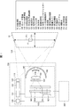
- FIG. 1 is a schematic diagram showing a configuration of an optical radar device 100 according to the present embodiment.
- the optical radar device 100 includes a pulsed light illumination system 110 that irradiates a target visual field 10 with pulsed light 124, and a light receiving system 140 that receives light from at least a part of the target visual field 10. Yes.
- the pulsed light illumination system 110 includes an illumination system power supply 120, a light emitting element driving circuit 121, a diffusion optical system 123, and a light emitting element 122.
- the diffusion optical system 123 collectively irradiates the entire target visual field 10 with the pulsed light 124 emitted from the light emitting element 122.
- the light emitting element driving circuit 121 is a circuit that drives the light emitting element 122 in pulses.
- the illumination system power source 120 is a power source that supplies power to the light emitting element driving circuit 121.
- the pulsed light illumination system 110 and the light receiving system 140 are provided close to each other. However, a structure in which the pulsed light 124 emitted from the pulsed light illumination system 110 does not leak into the light receiving system 140 except for the reflected light from the target object 11 to be detected in the target visual field 10 is preferable.
- the light receiving system 140 includes an imaging optical system 151, an optical band pass filter 152, a three-dimensional image element 153, a control element 160, and a light receiving system power supply 157.
- the three-dimensional image element 153 includes a light receiving unit 154 and a signal storage processing unit 155.
- the imaging optical system 151 forms an image of the reflected light from the target visual field 10 on the light receiving unit 154 of the three-dimensional image element 153.
- the control element 160 controls the three-dimensional image element 153 and the pulsed light illumination system 110 and communicates with the external system 300.
- the light receiving system power source 157 is a power source that supplies power to each unit of the light receiving system 140.
- the target visual field 10 is generally a rectangle characterized by a horizontal irradiation angle ⁇ h and a vertical irradiation angle ⁇ v, but is not limited to a rectangle and may be an elliptical shape.
- the pulsed light 124 is uniform in the target visual field 10, since the detection sensitivity of the place where the light intensity is strong becomes high, if there is a place that particularly needs to be watched in the target visual field 10, It is also possible to obtain a light intensity distribution with enhanced intensity in the vicinity.
- the diffusion optical system 123 is an optical system that irradiates and emits light from the light emitting element 122 into the target visual field 10, and includes a diffusion plate, a diffraction grating, a cylindrical lens, and the like.
- the light emitting element 122 is a light source capable of emitting pulses such as a laser and an LED, and preferably emits infrared light having a wavelength of about 700 nm to 1000 nm.
- an infrared laser is suitably used from the viewpoint that the light emission wavelength band is narrow and the temperature fluctuation of the light emission peak wavelength is preferably small.
- VCSEL Very / Cavity / Surface / Emitting / Laser
- a temperature control element that controls the temperature of the light emitting element 122 may be added to the pulsed light illumination system 110 in order to suppress temperature fluctuation of the emission peak wavelength.
- the light emitting element driving circuit 121 causes the light emitting element 122 to emit light in a pulsed manner by causing a predetermined current to flow through the light emitting element 122 at a predetermined timing.
- the light emission timing is determined by a signal from the control element 160.
- the amount of current of the light emitting element 122 may be variable or may be controlled by the control element 160. The same applies to the time change of the current that determines the emission time of the pulsed light 124.
- the half width (time) of the pulsed light 124 is about 1 nsec to several hundred nsec.
- the optical radar device 100 requires high-power pulsed light 124 of several tens to several hundreds W.
- the light emitting element driving circuit 121 generally discharges the charges to the light emitting element 122 at once after accumulating charges in the capacitor so as to form short pulse light. Therefore, the condenser and the switching element may be combined with the light emitting element 122 to be modularized.
- the illumination system power supply 120 has a normal logic circuit low voltage DC power supply and a high voltage DC power supply of several tens of volts for charging the capacitor. By controlling the output voltage of the high-voltage DC power supply or the charging time for the capacitor, the pulse emission power can be controlled. Further, the pulse width can be controlled by controlling the switching speed of the switching element. These controls can be performed by the control element 160.
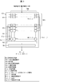
- FIG. 3 is a block diagram showing the configuration of the three-dimensional image element 153.
- FIG. 2 is a cross-sectional view of the package of the three-dimensional image element 153 constituting the optical radar device 100 according to the present embodiment.
- the imaging optical system 151 is generally a lens.
- the focal length and the F number can be selected depending on the size of the light receiving unit 154 and the viewing angle (FOV). It is preferable that the transmittance is high and the aberration is small at the center wavelength of the optical bandpass filter 152 described later.
- a lens is shown in FIG. 1, a reflective optical system other than a lens may be used instead of the lens.
- the optical bandpass filter 152 has a transmission band in a band with a constant width centering on the wavelength peak of pulsed light.
- the width of the transmission band (half width of the wavelength distribution of transmittance) is several nm to several tens of nm, and preferably about 10 nm to 20 nm.
- the peak temperature of the pulsed light changes with temperature due to the widening of the operating temperature range, so the pulsed light distribution needs to be within the transmission band at least in the operating temperature range. .
- the temperature shift of the peak wavelength is about 0.07 nm / degree
- the half width of the emission peak is about 1 nm
- the temperature shift of the transmission band center wavelength of the optical bandpass filter is 0.025 nm / degree. .
- the relative wavelength shift between the peak wavelength and the center wavelength of the transmission band is about 5.6 nm
- the optical bandpass filter has a transmission band of about 10 nm. 152 can be used.
- the flat interference filter When a flat interference filter generally used as the optical bandpass filter 152 is used, when the incident angle at which the reflected light is incident on the filter surface increases from 0 degree, the center wavelength of the transmission band shifts to the short wavelength side. Therefore, when the viewing angle is wide, the flat transmission filter may not be able to ensure the same transmission wavelength band in the entire target field 10.
- the flat interference filter is preferably shielded from the outside air because it may deteriorate and deteriorate over time when exposed to moisture or oxygen for a long time.
- a resin-made hemispherical dome transparent to infrared rays is provided as a protective cover 156 on the front surface of the imaging optical system 151 to protect the light receiving system 140 from the outside air.
- the protective cover 156 is provided, for example, the optical bandpass filter 152 can be provided on the surface of the imaging optical system 151 or the inner surface or inside of the protective cover 156.
- the optical bandpass filter 152 is provided on the protective cover 156, the hemispherical diameter of the protective cover 156 is set according to the diameter of the imaging optical system 151, so that each direction in the target visual field 10 can be set. A substantially constant transmission band can be secured for the reflected light.
- the diameter of the hemisphere As the diameter of the hemisphere is larger, the transmission band shift with respect to light condensed on each pixel Px (i, j) described later can be reduced. For this reason, the actual size of the diameter of the hemisphere can be determined by a trade-off between the outer shape of the optical radar device 100 and the reduction of the transmission band shift. In a practical range, the diameter of the hemisphere is preferably 5 times or more, more preferably 10 times or more the diameter of the imaging optical system 151.
- the optical bandpass filter 152 can be added inside the lid glass 171 as shown in FIG.
- the lid glass 171 constitutes an optical window of the package 170 that seals the three-dimensional image element 153.
- the sealed atmosphere 172 inside the package 170 preferably removes moisture and further preferably removes oxygen. This is to prevent the optical band pass filter 152 from aging. Therefore, the atmosphere 172 is preferably at least dry air, and more preferably nitrogen or argon, helium, or the like. Although omitted in FIG. 2, it is preferable to use a silicone resin with little oxygen and moisture permeation for bonding the lid glass 171 to the package 170.
- the optical band pass filter 152 may be incorporated in the imaging optical system 151. Although one optical bandpass filter 152 is shown in FIGS. 1 and 2, a plurality of optical bandpass filters 152 may be used.
- the first optical bandpass filter may be disposed on the front surface or the rear surface of the imaging optical system 151, and the second optical bandpass filter may be disposed on the inner surface of the lid glass 171 as described above. By providing the first optical bandpass filter, the light energy incident on the package 170 can be reduced, and an effect of suppressing a temperature rise can be obtained.
- the transmission band of the first optical bandpass filter is preferably wider than the transmission band of the second optical bandpass filter.
- the light receiving unit 154 and the signal storage processing unit 155 (integration unit and calculation unit) of the three-dimensional image element 153 can be formed on a silicon substrate.
- the light receiving unit 154 and the signal storage processing unit 155 are formed as separate chips, and may be combined using vertical via holes, bumps, and the like, and the respective chips may be stacked.
- the monolithic may be formed on the same silicon substrate. Preferably it is comprised.
- the light receiving unit 154 and the signal storage processing unit 155 are arranged in the upper and lower stages in the drawing. However, this is for the sake of convenience, and the light receiving unit 154 may be disposed in the center. However, it is not preferable that the light receiving unit 154 and the signal storage processing unit 155 are mixed. This is because the range in which the light receiving unit 154 exists is widened and the size of the imaging optical system 151 and the lid glass 171 is increased, resulting in an increase in cost.
- pixels Px (i, j) are arranged in a two-dimensional matrix of M rows and N columns.
- the pixel Px (i, j) has a function of detecting a photon by SPAD and outputting a pulse signal (pixel signal) as a photon detection result, as will be described later. All the pixels Px (i, j) are configured identically.
- the signal storage processing unit 155 includes a plurality of pixel storage elements Mx (i, j) (integrating units) corresponding to the respective pixels Px (i, j) arranged at least in a matrix.
- the pixel memory element Mx (i, j) is connected to each pixel Px (i, j) on a one-to-one basis by a signal line Lx (i, j).
- a photon (photon) is received by the pixel Px (i, j)
- a pixel signal (pulse signal) output as a photon detection result from the pixel Px (i, j) passes through the signal line Lx (i, j). Sent to the pixel storage element Mx (i, j) and stored therein.
- the signal storage processing unit 155 includes at least a row selection circuit 161 and a column selection circuit 162 (switching circuit) for selecting a specific pixel storage element Mx (i, j), and a signal processing circuit DS (calculation unit). Including.
- the signal processing circuit DS uses the distance information D (i, j) as an output signal based on the information stored in the specific pixel storage element Mx (i, j) selected by the row selection circuit 161 and the column selection circuit 162. ) And two-dimensional image information G1 (i, j), G2 (i, j) (two-dimensional image information) are calculated and output.
- the two-dimensional image information G1 (i, j), G2 (i, j) is the light intensity of the incident light (reflected light of the pulsed light) from the object 11 incident on each pixel Px (i, j). Is light intensity information for specifying a two-dimensional image of the object 11 based on each light intensity in the detection range.
- the difference between the two-dimensional image information G1 (i, j) and G2 (i, j) will be described later.
- the signal storage processing unit 155 is configured as follows.
- the row selection signal line R ⁇ (i) extends from, for example, the row selection circuit 161 to the pixel storage element Mx (i, j) in the i row.
- an ⁇ portion (a binary counter BC ⁇ described later) of the pixel storage element Mx (i, j) in the row i is selected.
- the column selection circuit 162 selects a specific column signal line C (j).
- the signal of the pixel storage element Mx (i, j) is read into the signal processing circuit DS, and the distance information D (i, j) and the two-dimensional image information G1 (i, j), G2 ( i, j) is output.
- the two-dimensional image information G1 (i, j) is two-dimensional image information (second light intensity information) of the object 11 with background light that does not include the reflected light of the pulsed light.
- the two-dimensional image information G2 (i, j) is two-dimensional image information (first light intensity information) of the object 11 by the reflected light of the pulsed light, but is not limited thereto.
- reading of the output signal from the pixel storage element Mx (i, j) is performed in parallel with the integration of the number of pulses of the pixel signal to the pixel storage element Mx (i, j). It can be carried out. As a result, a pixel with a strong signal intensity can be detected early.
- the pixel Px (i, j) having a high signal intensity captures a nearby object 11 and can detect the object 11 close to the three-dimensional image element at an early stage and issue an alarm. .
- the signal storage processing unit 155 stores the readout order of signals from the pixel storage element Mx (i, j), and can arbitrarily select the readout order. Thereby, the accumulated photons from the pixel storage element Mx (i, j) obtained by integrating the number of photons obtained from the pixel Px (i, j) from which the reflected light from the object 11 close to the three-dimensional image element is detected. The number can be read out early.
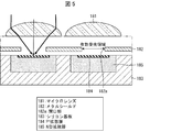
- FIG. 4 is a plan view showing the configuration of the pixel Px (i, j) of the three-dimensional image element 153.
- FIG. 5 is a cross-sectional view showing the configuration of the pixel Px (i, j).
- FIG. 6 is a circuit diagram showing the configuration of the pixel Px (i, j) of the three-dimensional image element 153.
- the light receiving unit 154 has a plurality of pixels Px (i, j) arranged in a two-dimensional matrix of M rows and N columns.
- the light receiving unit 154 is supplied with a control signal, a power supply voltage, a clock CLK, and the like.
- the pixel Px (i, j) is composed of one or a plurality of SPAD (Single-Photon-Avalanche-diode) 180 (avalanche photodiode).
- the SPAD 180 is a photodiode that detects photons of incident light in a Geiger mode.
- Each SPAD 180 has a microlens 181 as shown in FIG.
- the structure of the SPAD 180 can take various forms, but will not be described in detail here.
- the SPAD 180 is configured by forming a P + diffusion layer 184 on the surface of an N-type diffusion layer 185 formed on the silicon substrate 183.
- the surface of the silicon substrate 183 is covered with a metal shield 182 at a predetermined interval.
- the metal shield 182 has an opening 182 a formed so as to expose a part of the P + diffusion layer 184.
- the opening 182 a forms an effective light receiving region, and allows light incident through the microlens 181 to pass to the P + diffusion layer 184.
- each SPAD 180 is arranged at substantially the same distance except for the lower right of the pixel portion where the circuit such as the output circuit is arranged. This is because the microlens 181 is used to collect as much light as possible to increase detection sensitivity. However, if the sensitivity is sufficient and the pixel area can be reduced on the circuit layout, each SPAD 180 may be arranged in a concentrated range.
- the optimum value of the SPAD total number Nspad varies depending on the number of photons Md received by one pixel during the dead time Td of the SPAD 180 to be used.
- Deadtime Td is the time required for one SPAD to detect the next photon after detecting one photon, and literally the length of time that SPAD does not function as a sensor. Generally, the length is about several nsec to 100 nsec.
- Md ⁇ 1 the total SPAD Nspad may be small or one. However, in the case where the number of photons Md can exceed 1, the number of photons that can be counted is 1 because one SPAD 180 cannot measure the period of the next Td at the stage of counting the first one.
- the SPAD total number Nspad must be increased. If the fill factor (ratio of the total area of the effective light receiving region to the pixel area) is the same, the detection sensitivity improves as the SPAD total number Nspad increases.
- the pixel Px (i, j) includes a SPAD control unit 190 and a photon detection signal generation unit 191 as a part attached to each SPAD 180.
- FIG. 6 shows waveforms of signals output from the SPAD control unit 190 and the units of the photon detection signal generation unit 191, respectively.
- the SPAD control unit 190 is a circuit that applies the power supply voltage VSPAD to the SPAD 180, quenches when a photon is detected in the pixel Px (i, j), and returns to the measurement state after Deadtime Td.
- the SPAD control unit 190 is simply illustrated as a circuit to which one resistor R is added except for the SPAD 180, assuming an inactive quench, but an active quench circuit may be used.
- Various circuits such as a circuit for controlling the activation of the SPAD 180 can also be added.
- the photon detection signal generator 191 is a circuit that detects an increase in the terminal voltage of the SPAD 180 and outputs one pulse having a certain width when the SPAD 180 detects a photon.
- FIG. 6 shows an example in which the photon detection signal generator 191 includes a first inverter 192, a second inverter 193, a delay circuit 194, and a NOR circuit 195.
- the delay circuit 194 is shown in FIG. 6 as an example composed of two stages of inverters, it may be composed of four or more stages of even stages of inverters, or may be a delay circuit of another configuration.
- the delay time of the delay circuit 194 determines the pulse width. The delay time is preferably about 0.1 nsec to several nsec.
- the NOR circuit 195 outputs a logical sum negation of the output of the first inverter 192 and the output of the second inverter 193.
- the pixel Px (i, j) has a pixel signal output circuit 196 that is common to the photon detection signal generators 191.
- the pixel signal output circuit 196 is a circuit that receives the photon detection signals from the respective SPADs 180 in parallel and sends out a pulse having substantially the same length as the photon detection signal to the signal line Lx (i, j). If a plurality of SPADs 180 emit photon detection signals almost simultaneously, they cannot be distinguished. In order to minimize such a case, the pulse width of the signal passing through the signal line Lx (i, j) can be made as short as possible.
- 6 illustrates an example in which the pixel signal output circuit 196 includes a signal line drive circuit 197, a signal line reset circuit 198, and a delay circuit 199.
- the present invention is not limited to this.
- the signal line drive circuit 197 is a circuit that receives a photon detection signal, supplies a current to the signal line Lx (i, j), raises the potential of the signal line Lx (i, j), and outputs a pixel signal. It operates completely in parallel for each photon detection signal.
- the pixel signal is a pulse signal corresponding to the photon detection signal.
- the signal line drive circuit 197 has a configuration in which NMOS transistors having gates that receive outputs from the photon detection signal generation units 191 are connected in parallel, but other configurations may be used.
- the signal line drive circuit 197 may be configured to receive an output from each photon detection signal generation unit 191 by an AND circuit and turn on one NMOS transistor having a large driving capability by the output of the AND circuit.
- the signal line drive circuit 197 has a capability of driving the signal delay time in the signal line Lx (i, j) in a short time, and must transmit a signal to the pixel storage element Mx (i, j). This delay time is determined by the driving capability of the transistor provided in the signal line drive circuit 197 with respect to the parasitic capacitance of the signal line Lx (i, j). This delay time is preferably at least equal to or less than the pulse width generated by the photon detection signal generator 191.
- the signal delay time in the signal line Lx (i, j) is preferably short, and the signal line Lx (i, j) is short. Is preferred.
- the signal line reset circuit 198 is a circuit that restores the potential of the signal line Lx (i, j) after being raised by the signal line drive circuit 197.
- the signal line reset circuit 198 includes the delay circuit 199 that delays the signal of the signal line Lx (i, j) and the signal line pull-down circuit 200.
- the delay circuit 199 is shown as a two-stage inverter chain, it may be an even-numbered inverter chain of four or more stages, or may be another delay circuit.
- the photon detection signal is a pulse that rises from the ground level to the Vcc level, but the same function can be realized even if it is a pulse that falls from the Vcc level to the ground level.
- the pulse width of the pixel signal passing through the signal line Lx (i, j) is substantially determined by the photon detection signal generator 191, but is determined by the pixel signal output circuit 196. It is also possible to use a configuration.
- the signal line Lx (i, j) is shown as a single wiring, but a plurality of signal lines may be used.
- the signal line Lx (i, j) is a circuit configuration in which the pixel signal output circuit 196 generates a potential difference between the two lines based on the photon detection signal with two lines as a pair. It may be a signal line for transmission. Further, when the SPAD total number Nspad is large, the pixel signal output circuit 196 may be divided into a plurality of circuits, and a signal line may be provided for each of them.
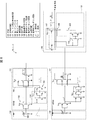
- FIG. 7 is a circuit diagram illustrating configurations of the pixel storage element Mx (i, j), the column selection circuit 162, and the signal processing circuit DS in the signal storage processing unit 155.
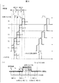
- FIG. 8A is a timing chart showing the drive timing of the pixel storage element Mx (i, j)
- FIG. 8B is a waveform diagram showing the reflected pulse light in an enlarged manner.
- the pixel storage element Mx (i, j) has a plurality of binary counters BC1 to BC ⁇ , a time switch 210, and an output switch 211.
- the binary counters BC1 to BC ⁇ are described as a representative, they are referred to as a binary counter BC ⁇ .
- the time switch 210 is a circuit including switches S1 to S ⁇ that selectively connect the signal line Lx (i, j) to the binary counters BC1 to BC ⁇ .
- the switches S1 to S ⁇ are composed of NMOS transistors. In the following description, when the switches S1 to S ⁇ are described as a representative, they are referred to as a switch S ⁇ .
- Binary counters BC1 to BC ⁇ are counters that count the pulse of the pixel signal from the pixel Px (i, j) input via the switches S1 to S ⁇ , respectively.
- the above pulses are input to the clock terminals of the binary counters BC1 to BC ⁇ .
- the reset signal Rf is input to the reset terminals R of the binary counters BC1 to BC ⁇ .
- the binary counters BC1 to BC ⁇ have output terminals of g1 bit, g2 bit,..., G ⁇ bit, respectively.
- the output switch 211 outputs the output of the binary counter BC ⁇ as a column signal when selected by the row selection signal line R ⁇ (j) (row selection signal lines R1 (j), R2 (j),..., R ⁇ 2 (j)).
- the output switch 211 is configured by an NMOS transistor having a gate connected to the row selection signal line R ⁇ (j), but is not limited thereto.
- One terminal of each NMOS transistor of the output switch 211 is connected to the output terminal of each bit of the binary counter BC ⁇ , and the other terminal is connected to the column signal line C (j).
- the binary counter BC ⁇ is connected to the signal line Lx (i, j) and accumulates the number of pulses transmitted from the pixel Px (i, j) for the time width ⁇ T ⁇ during which the switch S ⁇ is on.
- the output bit number g ⁇ of the binary counter BC ⁇ is determined by the maximum value of the number of photons to be measured.
- the column selection circuit 162 is a circuit that connects the column signal line C (j) to the signal processing circuit DS when selected by the column selection signal line CS (j).
- the NMOS transistor has a gate connected to the column selection signal line CS (j), but the present invention is not limited to this.
- the column selection circuit 162 connects column signal lines C (j + 1), C (j ⁇ 1) and the like arranged in parallel to the signal processing circuit DS.
- the reading order of the above-described integrated value of the number of photons from the pixel storage element Mx (i, j) is determined by selecting the output switch 211 by the row selection signal line R ⁇ (j) and each column signal line C by the column selection circuit 162. It is defined by the connection order of (j).
- the signal processing circuit DS can read the output of the binary counter BC ⁇ through the output switch 211 and the column signal line C (j) of the column selection circuit 162 even during integration by the binary counter BC ⁇ .
- the signals T1 to T ⁇ for driving the time switch 210 are signals for sequentially turning on the switches S1 to S ⁇ in time series as shown in FIG.
- the time widths ⁇ T1 to ⁇ T ⁇ for turning on the switches S1 to S ⁇ are equal to the half-value width ⁇ T of the pulsed light.
- the binary counters BC1 to BC ⁇ respectively count pulses and integrate the number of photons for each time period determined by the time widths ⁇ T1 to ⁇ T ⁇ .
- the binary counter BC1 measures the background light intensity. Therefore, the time width ⁇ T1 during which the switch S1 is turned on does not have to be the same as the on time ⁇ T ⁇ of the other switches S ⁇ .
- the noise level of the binary counter BC1 can be reduced by setting the length of the switch multiple times as long as the other switches S ⁇ are turned on. In that case, in the signal processing circuit DS, only the output value of the binary counter BC1 is divided by a multiple obtained by dividing the ON time length with respect to the other switch S ⁇ , and converted to data with the same time length as the other binary counter BC ⁇ . The trouble to do increases.
- the time widths ⁇ T2 to ⁇ T ⁇ are preferably equal to or less than the half-value width ⁇ T. Thereby, the influence of background light can be weakened and the signal-to-noise ratio of the signal can be improved.
- the time widths ⁇ T2 to ⁇ T ⁇ are longer than the half-value width ⁇ T, the influence of background light becomes strong, and the signal-to-noise ratio of the signal decreases.
- the time widths ⁇ T2 to ⁇ T ⁇ are twice as long as the half-value width ⁇ T, the background light measurement time is doubled with respect to the time during which the reflected light of the pulse light may be detected.
- the intensity ratio of the reflected pulse light to the background light is 1 ⁇ 2 compared to when the time width ⁇ T2 to ⁇ T ⁇ is substantially the same as the half-value width ⁇ T. Therefore, the detection sensitivity is deteriorated with respect to the far object 11 whose reflected light of the pulsed light is weaker than the background light.
- the binary counter BC2 receives the pulsed light reflected in an extremely short time as a light reception signal. That is, when the object 11 is located very close to the three-dimensional image element 153, the count number of the binary counter BC2 increases with respect to the count number of the binary counter BC1. With respect to the distance L between the object 11 and the three-dimensional image element 153, the reflected light of the pulsed light reaches the three-dimensional image element 153 after 2L / c (c: speed of light). A light reception signal having an intensity higher than that of the background light is input to the binary counter (the binary counters BC3 and BC4 in the example of FIG. 8A).
- the above integration is executed for a plurality of pulsed light emitted during one frame (for example, 1/30 sec). That is, a series of integrated values arranged in a time series acquired by the three-dimensional image element every time a plurality of times of pulsed light irradiation are integrated with each other.
- the data stored in each binary counter BC ⁇ is read out to the signal processing circuit DS, and then activated by the reset signal Rf, the count number up to that point is cleared, and the next frame is cleared. Ready to start measuring.
- the binary counter total number ⁇ has the following relationship with respect to the maximum measurement distance Dmax and the half-value width ⁇ T.
- the distance measurement accuracy can be improved by reducing the half-value width ⁇ T and increasing the total number of binary counters ⁇ .
- the binary counter total number ⁇ increases, the area of the pixel storage element Mx (i, j) increases, leading to an increase in the area of the chip constituting the three-dimensional image element 153 and an increase in the cost of the optical radar device 100. .
- the pixel storage element Mx (i, j) and the signal processing circuit DS are basically logic circuits, the area can be reduced by adopting a silicon LSI manufacturing process that has been miniaturized. Since the manufacturing cost of such a miniaturization process is decreasing year by year, the total number of binary counters ⁇ can be increased from tens to hundreds in the future.
- the signals T1 to T ⁇ do not overlap each other in principle and cover the time zone to be measured without omission, but in FIG. Since the processing can be simplified, the pulse widths to be activated are made equal to each other. However, the pulse widths to be activated are not necessarily limited to the case where they are equal to each other. For example, in order to improve the distance measurement accuracy for a short distance, the pulse width can be shortened at the first part of the lapse of time, and gradually increased with the lapse of time, or can be changed in a plurality of stages.
- the signals T1 to T ⁇ must be distributed to all the pixel storage elements Mx (i, j), there is a possibility that a slight error may occur in the wiring delay due to the variation in the delay between the wirings. Since the error in the pulse width for activating the signals T1 to T ⁇ is directly related to the accuracy of the distance measurement value, it is necessary to adopt a circuit configuration and wiring arrangement with high time accuracy according to the accuracy required for the optical radar device 100. There is.
- the switches S1 to S ⁇ constituting the time switch 210 are directly turned on / off by the signals T1 to T ⁇ in the example shown in FIG. 7, but may be configured by other circuits.
- a configuration in which each output of a simple shift register (the number of bits; ⁇ ) is connected to the switches S1 to S ⁇ and the ON state is sequentially shifted by a clock signal may be employed.
- the number of signals can be reduced, and only one of the switches S1 to S ⁇ can be reliably turned on. Therefore, for the switch S ⁇ and the switch S ( ⁇ + 1) that are adjacent to each other in the ON time zone, the counting error can be reduced by preventing the opening of the ON time zone or the occurrence of overlap.
- the time switch 210 may have any configuration as long as it is a circuit in which the opening time or overlap between adjacent switches is small.
- the binary counter BC ⁇ is used as a circuit for counting the pulse signal generated when the light receiving unit 154 detects photons in time series. This is because the binary counter BC ⁇ can be configured with a relatively simple circuit, and when configured as an integrated circuit, a function of counting and integrating with a small area can be realized. Another reason is that since the binary counter BC ⁇ is a simple logic circuit, it is easy to obtain a wide operation margin and the design is easy.
- the binary counter BC ⁇ has such advantages, but the pixel storage element Mx (i, j) does not necessarily need to be configured by a plurality of binary counters BC1 to BC ⁇ .
- any other configuration may be used as long as it is a circuit that integrates and stores the number of detected photons for each of a series of time intervals arranged almost continuously in time series in combination with the time switch 210. Further, it is preferable that the integration result during the integration can be read without greatly affecting the integration operation.
- the count number NC ⁇ (t) of pulses by each binary counter BC ⁇ at a certain time t is a count number NC1 (t), NC2 (T) and NC5 (t) are substantially equal values except for noise, and both represent the background light intensity.
- the count numbers NC3 (t) and NC4 (t) include the reflected light of the pulse light and are significantly larger than the count numbers NC1 (t), NC2 (t), and NC5 (t). Accordingly, the distance between the light receiving unit 154 and the object 11 is calculated by the following equation.
- the integer 8B it is “1”. However, the above number is an integer greater than or equal to 0. If the object is at a long distance, the integer increases, and decreases at a short distance.
- A is an integrated value of the reflected pulse light intensity measured during the timing T3
- B is an integrated value of the reflected pulse light intensity measured during the timing T4. Since the pulse width of the pulsed light and the time length to be measured are the same, as shown in FIG. 8B, the reflected light is detected only in at most two adjacent sections. Therefore, the length of the period Tb is similarly calculated from the intensity of the reflected light of the pulse light regardless of the distance of the object. Also, the above equation is divided by 2 because light travels back and forth between the object 11 and the object Ta 11 in a period that combines the period Ta and the period Tb, so that the distance to the object 11 is divided by 2. It is necessary.
- the signal processing circuit DS can output D (t) as the distance signal D (i, j) to each pixel Px (i, j).
- the signal processing circuit DS can output the following information as the two-dimensional image information G1 (i, j), G2 (i, j).
- G1 (i, j) NC1 (t)
- an integrated value larger than the noise level is obtained from the pulse count number NC ⁇ (t)
- a pair of the obtained integrated value and the integrated value temporally adjacent to each other is obtained, and the count number is obtained.
- the distance to the object can be calculated with an accuracy shorter than the time interval.
- the flight time with an accuracy of c ⁇ ⁇ T / 2 or less is obtained. It becomes possible to determine (the part other than the integer in [] of D (t)), and the distance measurement accuracy to the object can be improved.
- FIG. 9 is a flowchart showing a procedure of signal processing by the signal processing circuit DS.
- the signal processing circuit DS may serially process the output signal of each pixel Px (i, j), or may have a plurality of arithmetic circuits and process the output signal of each pixel Px (i, j) in parallel. You may do it.
- the signal processing circuit DS reads the count numbers NC1 (t) to NC ⁇ (t) from the pixel storage element Mx (i, j), and stores them in the memory in the signal processing circuit DS (step S221).
- the signal processing circuit DS determines the noise level ⁇ N (t) (step S222).
- there are various noises such as dark current noise, 1 / f noise, thermal noise, etc., but the largest noise in the photon quantity measurement is shot noise.
- shot noise proportional to ⁇ N is attached to the number of detected photons N (average value).
- the count number NC ⁇ (t) must be considered to have noise proportional to ⁇ NC ⁇ (t).
- a ⁇ N (t) A ⁇ ⁇ NC1 (t) + B (B is a constant)
- A is preferably 3 or more, and more preferably 4 or more.
- B is a noise component other than shot noise, such as dark current noise.
- the count number NC1 (t) that does not include the reflected light of the pulse light and includes only the background light signal is used.
- the noise level ⁇ N (t) is determined by other methods. You may decide. For example, the count number NC ⁇ (t) is measured from the count number NC2 (t) without measuring the count number NC1 (t), and the average value Ave (NC ⁇ ) of the count number NC ⁇ (t) from the count number NC2 (t) Based on (t)), the calculation may be performed based on the following equation.
- ⁇ N (t) A ⁇ ⁇ Ave (NC ⁇ (t)) + B
- Ave (NC ⁇ (t)) is very close to the average value of background light.
- Ave (NC ⁇ (t)) decreases.
- NC ⁇ (t) In calculating the average value of NC ⁇ (t), some average values may be used instead of all the average values from NC2 to NC ⁇ . Further, when obtaining ⁇ N (t) using Ave (NC ⁇ (t)), BC1 for obtaining NC1 (t) can be omitted.
- the circuit scale increases and the calculation time becomes long. Therefore, an approximate value can be used instead.
- the noise level ⁇ N (t) when the most significant bit of the count number NC1 (t) is in the k-th digit, the number having the most significant bit in the k / 2 digit (rounded up when k is an odd number) is defined as the noise level ⁇ N (t).
- an approximation method is used such that a noise level ⁇ N (t) is a number having the most significant bit in the k / 2 digit (rounded up when k is an odd number) and the lower order bit is 1. It is also possible.
- step S223 a loop process for searching for an item significantly larger than the count number NC1 (t) from the count number NC2 (t) to the count number NC ⁇ (t) is executed (steps S223 to S226).
- the signal processing circuit DS sets the initial value of ⁇ to, for example, 2 at the beginning of this loop processing (step S223), and then determines whether ⁇ is equal to or less than the total binary counter ⁇ (step S224).
- step S224 when the signal processing circuit DS determines that ⁇ is equal to or smaller than the binary counter total number ⁇ (YES in step S224), the signal processing circuit DS determines whether or not the condition represented by the following equation is satisfied for ⁇ (step S224). Step S225).
- step S224 when the signal processing circuit DS determines that the condition represented by the above expression is satisfied for the above ⁇ (YES in step S225), ⁇ at that time is set to ⁇ (step S226). On the other hand, when the signal processing circuit DS determines in step S224 that the condition represented by the above expression is not satisfied for the above ⁇ (NO in step S225), 1 is added to ⁇ at that time (step S225). S227) The process returns to step S224.
- the count number NC ⁇ (t) is an integrated value larger than the noise level, and the count number NC ( ⁇ + 1) (t) is an integrated value that is temporally adjacent. A pair of count number NC ⁇ (t) and count number NC ( ⁇ + 1) (t) is extracted.
- the signal processing circuit DS calculates the measurement result according to the following equation when ⁇ is determined (step S228).
- IC (t) NC ⁇ (t) + NC ( ⁇ + 1) (t) ⁇ 2 ⁇ NC1 (t)
- D (t) c ⁇ ⁇ T ⁇ [( ⁇ 2) + ⁇ NC ( ⁇ + 1) (t) ⁇ NC1 (t) ⁇ / IC (t)] / 2
- the signal processing circuit DS obtains the next distance information D (i, j) and two-dimensional image information G1 (i, j), G2 (i, j) based on the result of the above calculation (step S229).
- the signal processing circuit DS stores the calculated distance information D (i, j) and the two-dimensional image information G1 (i, j), G2 (i, j) in a memory and outputs them to the external system 300 as appropriate.
- the signal processing circuit DS calculates and stores the distance information D (i, j) and the two-dimensional image information G1 (i, j), G2 (i, j) and stores them in the external system 300. Output.
- the specific calculation method of the distance information D (i, j) and the two-dimensional image information G1 (i, j), G2 (i, j) by the signal processing circuit DS is not limited to this, and various algorithms are adopted. Is possible.
- the SNR can be improved and the distance information can be obtained by integrating the measurement results (number of photons) of many laser pulse lights by the binary counter BC ⁇ .
- the intensity of the background light is 100
- the intensity of the reflected light of the pulsed light is 10
- the intensity of the reflected light is almost the same as the noise of the background light and cannot be reliably detected by one measurement.
- the measurement results of 100 times are integrated, the intensity of the background light is 10,000 and the shot noise is on the order of 100.
- the intensity of the reflected light of the pulsed light is 1000, which is an order of magnitude larger than the noise of the background light, and is a value that can be reliably detected.
- a mechanism for performing this integration digitally and in parallel for all the pixels Px (i, j) can be realized with silicon. Therefore, even in an environment with strong background light, the optical radar device 100 that extends the distance measurement range can be provided at a low cost.
- the pixel storage element Mx (i, j) of the present embodiment has a function in which the binary counter BC ⁇ counts the number of photons detected as electric pulses by the pixel Px (i, j), and the signal processing circuit DS The function of reading the count result can be executed in parallel. As a result, the measurement result cannot be taken out until one frame is completed, and the measurement result can be taken out even in the middle of one frame.
- the frame frequency is 30 Hz
- 1/30 (second) time can be used to acquire one frame of data
- the object 11 is located at a short distance, data may be obtained even with one pulse emission.
- the far object 11 cannot obtain data unless a large number of pulse emission data are accumulated.
- information on the object 11 close to the optical radar device 100 can be output earlier by obtaining an intermediate measurement result.
- collisions can be prevented by detecting an object closest to a car or robot on which the optical radar device 100 is mounted as early as 1/30 (second) and issuing an alarm to a control system of the car, robot, or the like.
- the relative speed with the object 11 in a short distance of several meters reaches 100 km / h. If the speed is 30 km / h, the distance moved in 1/30 (second) is about 30 cm, and the time is short. However, the possibility of avoiding a collision can be increased.
- the two-dimensional image information G1 (i, j) is information based on background light and is useful for recognizing the shape and the like of the object 11. It is. In particular, when information from a normal image sensor is used together, the information is compared with the two-dimensional image information G1 (i, j), and the object 11 common to both is specified. Recognition of the object 11 and acquisition of the distance between the object 11 and the light receiving unit 154 can be performed. Furthermore, when it is difficult to specify the distance due to a large error, the approach of the object 11 can be determined by capturing the time passage of the two-dimensional image information G2 (i, j).
- the two-dimensional image information G2 (i, j) may be compared between consecutive frames or between distant frames, or may be compared for each of a plurality or a single pulse emission.
- the signal processing circuit DS reads the count number of the number of photons for the pixel Px (i, j) of M rows and N columns in any order, and the distance information D (i, j) and two-dimensional based on the count number You may control the procedure of calculating image information G1 (i, j), G2 (i, j). Further, the signal processing circuit DS may have a memory used for the control. Further, the signal processing circuit DS may control the timing for counting the photon detection signal of the pixel Px (i, j). This control is, for example, a control in which the activation time of the signal T1 shown in FIG. 8 is made several times the activation time of the other signal T ⁇ in order to measure the background light signal with high accuracy.
- the signal processing circuit DS may control the timing for generating the pulsed light, or may control the timing for activating the pixel Px (i, j). For example, the signal processing circuit DS activates the pixel Px (i, j) to measure the above-described background light, stores the count number in BC1 during the time width ⁇ T1, and the time of the time width ⁇ T1 has elapsed. At that time, a signal is emitted to the pulsed light illumination system 110 via the control element 160 so that the pulsed light is emitted. Thus, the signal T2 is activated when the time width ⁇ T1 has elapsed.
- the signal storage processing unit 155 or the control element 160 has a memory for storing at least distance information D (i, j) and two-dimensional image information G1 (i, j) and G2 (i, j) information of all pixels. May be.
- the signal processing circuit DS may sequentially store the obtained information in this memory, and may output the information to the external system 300 via the control element 160 in response to a request from the external system 300. Further, when the signal processing circuit DS has memories for a plurality of frames, the signal processing circuit DS may further output the results of comparison and calculation between the frames.
- ⁇ Effect verification> A prototype was produced based on the above embodiment, and its characteristics were evaluated.
- the pulsed light illumination system 110 three VCSELs having a peak wavelength of 945 nm were used as the light emitting elements 122, and each pulse peak output was set to 25 W, and the pulsed light illumination system 110 was driven to emit light with a pulse half width of 100 nsec.
- the irradiation intensity at the center of the irradiation region was the highest at 12 ⁇ W / cm 2, the irradiation intensity at the four corners was the lowest, and the minimum was 10.6 ⁇ W / cm 2.
- the maximum and minimum values were within ⁇ 10% of the average value.
- the repetition emission frequency of the laser pulse was set to 19 kHz in consideration of class 1 conditions. Assuming image acquisition at 30 frames per second, data can be stored for a maximum of 633 laser pulse emissions per frame.
- the imaging optical system 151 of the light receiving system 140 a lens having a focal length of 4.5 mm, an F number of 1.8, and an effective diameter of 2.5 mm was used.
- the optical bandpass filter 152 an interference filter was used in which the center wavelength was selected so that the peak wavelength of the laser coincided with the center value of the transmission band at room temperature.
- the interference filter was coated on the inside of a lid glass 171 that hermetically seals a package 170 that houses the three-dimensional image element 153. Nitrogen having a low dew point was used as the atmosphere 172 in the package.
- the half band width of the transmission band of the interference filter was 10 nm, and the average transmittance was 55%. Since the temperature dependency of the emission peak wavelength of VCSEL is 0.07 nm / K and the center value of the transmission band of the interference filter is 0.025 nm / K, the relative value of the laser peak wavelength and the center value of the interference filter transmission band is The deviation was ⁇ 2.8 nm between 85 ° C. and ⁇ 40 ° C. This deviation is within the transmission band width of 10 nm even when the half-value width of 1 nm of the laser emission peak is included, and the VCSEL can be used without any temperature control. It is important to match the emission peak wavelength of the light emitting element 122 with the transmission band center value of the optical bandpass filter 152 near the temperature located in the center of the temperature band to be used.
- the light receiving unit 154 of the three-dimensional image element 153 50 ⁇ m square pixels Px (i, j) are arranged such that 180 effective pixels in the horizontal direction and 40 effective pixels in the vertical direction are arranged. It was composed of a total of 7.2k effective pixels.
- each SPAD 180 is provided with a microlens 181 having a base size of 15 ⁇ m.
- the height of the microlens was about 10 ⁇ m.
- the fill factor of this pixel Px (i, j) was 22%.
- Each SPAD 180 was operated with a deadtime Td of 20 nsec.
- the effective quantum efficiency of SPAD180 having this microlens 181 was 10%.
- the number of photons received by the background light measured on a white plate with a reflectance of 50% with respect to 945 nm infrared light at noon in fine weather was 0.29 per SPAn180 and 100 nsec on average. Therefore, the average number of photons detected from the background light of all seven SPADs was 1.9 per 100 nsec.
- counting with a pulse of a 1.0 nsec width pixel signal a plurality of photons are detected almost simultaneously, and there is a possibility of undercounting about 2%, but this is not a numerical value that greatly affects the count result.
- the signal storage processing unit 155 when the signal storage processing unit 155 is arranged on one side of the light receiving unit 154, it is necessary to arrange at least 40 wires in a width of 50 ⁇ m. If the wiring is arranged at a pitch of 1 ⁇ m, a single-layer wiring can be realized. However, since a power supply line and other wirings are also necessary, the signal line Lx (i, j) is configured by two layers of the upper-layer wiring.
- the wiring delay time becomes the drive capability rate limiting of the signal line drive circuit 197 that charges the parasitic capacitance of the signal line Lx (i, j).
- the area that can be used for the signal line drive circuit 197 is limited, and a delay time of about several hundred psec occurs. Therefore, the delay time of the delay circuit 194 of the photon detection signal generator 191 shown in FIG. 6 is set to 500 psec. On the other hand, the delay time of the delay circuit 199 of the pixel signal output circuit 196 is set to 700 psec.
- the image storage element Mx (i, j) shown in FIG. 7 has four binary counters BC1 to BC4.
- the binary counters BC1 and BC4 are 12-bit binary counters
- the binary counter BC2 is a 16-bit binary counter
- the binary counter BC3 is a 13-bit binary counter.
- the number of bits is increased because there is a possibility that the count number may be increased by receiving strong laser pulse reflected light from the object 11 with a short distance from the three-dimensional image element 153.
- the row selection circuit 161 sequentially selects the row selection signal lines R1 (i), R2 (i), R3 (i), and R4 (i) for each row.
- the output switch 211 outputs the output data of the corresponding binary counters BC1, BC2, BC3, and BC4, respectively.
- the signal processing circuit DS has only one arithmetic circuit in order to reduce the circuit scale.
- the signal processing circuit DS is composed of a memory for temporarily storing data of the binary counters BC1 to BC4, a 16-bit microcomputer for executing a distance calculation, and the like.
- the algorithm used for distance extraction can be changed by using a microcomputer.
- a microcomputer with a bit number (in this case, 16 bits) that is greater than or equal to the maximum number of bits of the binary counters BC1 to BC4
- the speed of distance extraction can be improved, and the time between pulse emission (about 50 ⁇ sec) Distance extraction for all pixels is possible.
- the design period is shortened, but the area of the signal processing circuit DS is increased and the cost is increased.
- a dedicated circuit can be designed.
- the signal processing circuit DS can program in what order the pixel storage elements Mx (i, j) are processed using the function of the microcomputer.
- the pixel storage elements Mx (i, j) are processed using the function of the microcomputer.
- the optical radar device 100 used for monitoring the surroundings of an automobile, normally there is a higher possibility that an obstacle appears at the lower end than at the upper end of the field of view. In this case, it is preferable to process from the lower part of the visual field to the upper part.
- an obstacle can be detected earlier by checking from the left end of the field of view when the vehicle moves backward.
- the vicinity of the person can be intensively checked.
- the signal processing circuit DS has a memory (230 kb) having a capacity of 32 bits for each pixel Px (i, j). This memory accumulates the two-dimensional image information G2 (i, J) between frames, thereby improving the accuracy of distance information, storing the integrated value, and comparing it with another measured value or integrated value. By doing so, it is possible to detect approach and departure.
- the signal processing circuit DS When the signal processing circuit DS is laid out by a process of 0.13 ⁇ m, the area of the signal processing circuit DS is 2 mm ⁇ 2 mm, and the area of the pixel storage element Mx (i, j) is 50 ⁇ m ⁇ 20 ⁇ m. The size of 153 was 10 mm ⁇ 5.5 mm.
- the signal processing circuit DS also includes a non-volatile memory for storing operation conditions such as a distance extraction algorithm and a scanning order of the pixel storage element Mx (i, j).
- a white plate having a reflectance of 50% with respect to 945 nm infrared light was used as the object 11, and pulsed light was examined in a measurable range under three conditions: clear sky, cloudy, and nighttime.
- the average count values of binary counters BC1, BC2, BC3, and BC4 obtained by one-time pulse light irradiation are 1.9, 7.5, and 2.0 at a distance of 2 m, respectively. 1.9, and it was possible to capture the presence of the object 11 in the vicinity. As a result, the object 11 up to 3.5 m could be detected. Therefore, it is possible to capture where the nearest object 11 is in this way from the measurement result of one pulsed light, and transmit the result to the external system 300.
- the difference between the binary counter BC3 and the binary counter BC1 is an error range in one measurement, and the distance between the light receiving unit 154 and the object 11 cannot be specified.
- the distance increases when the count number of the binary counter BC2 corresponding to the same pixel Px (i, j) increases. It can be judged that it is approaching and is moving away when it decreases. Based on such determination, it is useful to output the pulsed light reflection intensity for each frame.
- the three-dimensional image element 153 of this embodiment can collect the surrounding three-dimensional information including distance information. it can.
- Embodiment 2 The following describes Embodiment 2 of the present invention with reference to FIG.
- FIG. 10 is a flowchart showing a signal processing procedure by the signal processing circuit DS in the three-dimensional image element 153 of the optical radar device 100 according to the present embodiment.
- the optical radar device 100 according to the present embodiment is the same as that of the first embodiment except that the distance extraction algorithm of the signal processing circuit DS is different from that of the first embodiment.
- the distance extraction algorithm of the first embodiment is simple, but the difference between the count number NC ⁇ (t) and the count number NC1 (t) is small, or the difference between NC ( ⁇ + 1) (t) and NC1 (t) is If it is small, it is susceptible to measurement errors. The algorithm described below improves this point.
- FIG. 10 is a schematic diagram showing a procedure of signal processing by the signal processing circuit DS in the three-dimensional image element 153 of the optical radar device 100 according to the present embodiment.
- the signal processing circuit DS first performs the processes of steps S221 and S222 shown in FIG. 9, and then executes a loop process for searching for the maximum value of NC ⁇ (t) (steps S240 to S243). .
- the signal processing circuit DS sets the initial value of ⁇ to 2, for example, and sets the initial value of ⁇ to 1 (step S240).
- ⁇ is equal to or less than the total number of binary counters ⁇ . Whether or not (step S241).
- step S241 when the signal processing circuit DS determines that ⁇ is equal to or smaller than the total number of binary counters ⁇ (YES in step S241), it is determined whether or not ⁇ and ⁇ satisfy the condition represented by the following expression. Determination is made (step S242).
- step S242 when the signal processing circuit DS determines that the above-described conditions for ⁇ and ⁇ are satisfied (YES in step S242), ⁇ at that time is set to ⁇ (step S243). . On the other hand, when the signal processing circuit DS determines in step S242 that the above-described conditions for ⁇ and ⁇ are not satisfied (NO in step S242), the value of ⁇ is not changed. In either case (YES and NO in step S242), 1 is added to ⁇ at that time (step S244), and the process returns to step S241.
- step S241 when the signal processing circuit DS determines that ⁇ exceeds the binary counter total number ⁇ (NO in step S241), the maximum value of NC ⁇ (t) is determined and the value of ⁇ is also determined. .
- the signal processing circuit DS determines whether or not ⁇ satisfies the condition expressed by the following equation, that is, the difference between the count number NC ⁇ (t) and the count number NC1 (t) is a noise level ⁇ N. It is determined whether it is larger (step S245).
- step S245 when the signal processing circuit DS determines that the above ⁇ satisfies the condition expressed by the above equation (YES in step S245), the count number NC ⁇ (t) is significantly greater than the count number NC1 ( It can be said that it is larger than t). In this case, the signal processing circuit DS further determines whether or not the above ⁇ satisfies the condition expressed by the following equation (step S246).
- step S246 when the signal processing circuit DS determines that the condition represented by the above expression is satisfied for the above ⁇ (YES in step S246), ⁇ is set to ⁇ + 1 (step S247). In step S246, when the signal processing circuit DS determines that the condition represented by the above equation is not satisfied with respect to ⁇ (NO in step S246), ⁇ is set to ⁇ 1 (step S248).
- the signal processing circuit DS determines whether or not the condition represented by the following equation is satisfied with respect to ⁇ , that is, the difference between the count number NC ⁇ (t) and the count number NC1 (t). Is greater than the noise level ⁇ N (step S249).
- step S249 if the signal processing circuit DS determines that the above ⁇ does not satisfy the condition expressed by the above equation (NO in step S245), the count number NC ⁇ (t) is significantly greater than the count number NC1 ( It cannot be said that it is larger than t). In this case, when ⁇ and ⁇ are determined, the signal processing circuit DS calculates the measurement result according to the following equation (step S250).
- the signal processing circuit DS obtains the next distance information D (i, j) and two-dimensional image information G1 (i, j), G2 (i, j) based on the result of the above calculation (step S251).
- the signal processing circuit DS stores the calculated distance information D (i, j) and the two-dimensional image information G1 (i, j), G2 (i, j) in a memory and outputs them to the external system 300 as appropriate.
- step S249 if the signal processing circuit DS determines that the above condition is satisfied (YES in step S249), it can be said that the count number NC ⁇ (t) is significantly larger than the count number NC1 (t). In this case, the signal processing circuit DS determines whether or not ⁇ is smaller than ⁇ (step S252).
- step S252 when the signal processing circuit DS determines that ⁇ is smaller than ⁇ , the signal processing circuit DS calculates the measurement result according to the following equation (step S253), and the process proceeds to step S251.
- step S252 NC ⁇ (t) + NC ⁇ (t) ⁇ 2 ⁇ NC1 (t)
- D (t) c ⁇ ⁇ T ⁇ [( ⁇ 2) + ⁇ NC ⁇ (t) ⁇ NC1 (t) ⁇ / IC (t)] / 2 If the signal processing circuit DS determines in step S252 that ⁇ is not smaller than ⁇ ( ⁇ is greater than or equal to ⁇ ), the signal processing circuit DS calculates the measurement result according to the following equation (step S254), and the process proceeds to step S251. To do.
- the signal processing circuit DS calculates and stores the distance information D (i, j) and the two-dimensional image information G1 (i, j), G2 (i, j) and stores them in the external system 300. Output.
- the distance and the like are calculated by the equations of steps S253 and S254, respectively, according to the magnitude relationship between ⁇ and ⁇ (step S252). Thereby, the distance with the highest accuracy can be obtained.
- FIG. 11 is a block diagram showing a configuration of the three-dimensional image element 153 constituting the optical radar device 100 according to the present embodiment.
- the essential difference between the present embodiment and the first embodiment is that the maximum number of binary counters BC ⁇ constituting the pixel memory element Mx (i, j) is increased to 21.
- the algorithm of Embodiment 2 was used for the distance estimation algorithm. The details will be described below.
- the three-dimensional image element 153 includes divided signal storage processing units 155a and 155b.
- the signal storage processing units 155a and 155b are arranged on both sides of the light receiving unit 154, the signal storage processing unit 155a is arranged on the lower side in the drawing, and the signal storage processing unit 155b is arranged on the upper side in the drawing.
- the light receiving unit 154 is not essentially changed from the light receiving unit 154 in the first embodiment.
- the signal storage processing unit 155a performs signal processing of 20 rows of pixels Px (i, j) located in the half of the signal storage processing unit 155a side in the light receiving unit 154.
- the signal storage processing unit 155b performs signal processing of 20 rows of pixels Px (i, j) located in the half of the signal storage processing unit 155b side in the light receiving unit 154.
- the number of bits of the binary counter BC ⁇ is changed for each binary counter from 16 bits to 12 bits in consideration of the maximum signal value that can be counted by each binary counter BC ⁇ .
- the numbers of bits of the binary counters BC1, BC2, BC3, BC4, and BC5 are 16 bits, 17 bits, 15 bits, 14 bits, and 13 bits, respectively.
- the number of bits of the binary counters BC6 to BC22 is 12 bits.
- the number of binary counters BC1 to BC21 increases greatly, the number of transistors constituting the time switch 210 connected to the signal line Lx (i, j) increases. As a result, the load on the signal line Lx (i, j) increases and the signal delay may increase, so a buffer is added at the forefront of the time switch 210. This is because the area of the pixel memory element Mx (i, j) is increased, and thus the wiring length of the signal line Lx (i, j) is increased.
- the signal storage processing units 155a and 155b have row selection circuits 161a and 161b, column selection circuits 162a and 162b, column signal lines Ca (j) and Cb (j), and signal processing circuits DSa and DSb, respectively. is doing.
- the signal processing circuits DSa and DSb each have the same capability for data processing because the amount of data to be handled increases. Therefore, the signal storage processing units 155a and 155b can perform data processing of the respective areas in parallel.
- the signal processing circuits DSa and DSb each have one arithmetic circuit. However, laser light emission timing control, pixel Px (i, j) activation timing control, signal readout from pixels Px (i, j) of M rows and N columns (array), calculation procedure control, memory Only the signal processing circuit DSa has functions such as management and output control.
- the three-dimensional image device 153 identified the object 11 up to 19 m under the maximum integration condition of a 1/30 sec frame period in the daytime in fine weather.
- the maximum measurement error at a distance in the range of more than 6 m and 19 m or less was 1 m.
- the maximum measurement error at a distance in the range of 6 m or less and 1 m or more was 0.31 m. For distance measurement exceeding 9 m, it was difficult in Embodiment 1 to refer to the time change of IC (t), but in this embodiment, it can be measured up to 19 m although there is an error.
- the measurement accuracy by the three-dimensional image element 153 of the present embodiment is improved even in cloudy weather and at night.
- the three-dimensional image element 153 recognizes the object 11 that is separated up to 30 m, and the maximum distance measurement error up to 30 m is 0.5 m.
- the three-dimensional image element 153 recognizes the object 11 separated to a distance of 30 m, and the maximum measurement error is 0.3 m.
- the object 11 up to 3 m was captured by accumulating 10 pulsed emissions, and the distance could be measured with a maximum error of 0.5 m.
- accumulation of signals in the pixel storage element Mx (i, j) by 100 pulses could be measured with a maximum error of 0.27 m within a distance of 3 m.
- the distance measurement is difficult, but in the present embodiment, it is improved so that the distance can be measured in a short time while being rough.
- Embodiment 4 The following describes Embodiment 4 of the present invention.
- This embodiment is different from the third embodiment in the following points, but other than that is basically unchanged from the third embodiment.
- the number of bits of the binary counter BC ⁇ constituting the pixel storage element Mx (i, j) is unified to 12 bits for all the binary counters BC ⁇ to facilitate the design.
- the memory (230 kb) having a capacity of 32 bits for each pixel Px (i, j) included in the signal processing circuit DS described in the first embodiment may be diverted to the present embodiment or newly added to each pixel.
- a memory (86 kb) having a capacity of 12 bits may be added.
- 12 bits is a sufficient number of bits to describe a distance of up to 30 m as a 2-bit integer in centimeters.
- the function of the signal processing circuit DS shown in FIG. 3 and the signal processing circuits DSa and DSb shown in FIG. 11 may be realized by a logic circuit (hardware) formed in an integrated circuit (IC chip) or the like. As described above, the function may be realized by software using a microcomputer.
- the signal processing circuits DS, DSa, DSb can be read by a CPU (Central Processing Unit) that executes instructions of a program that is software that implements each function, and the program and various data can be read by a computer (or CPU). It includes a recorded ROM (Read Only Memory) or a storage device (these are referred to as “recording media”), a RAM (Random Access Memory) for expanding the program, and the like. And the objective of this invention is achieved when a computer (or CPU) reads the said program from the said recording medium and runs it.
- ROM Read Only Memory
- storage device these are referred to as “recording media”
- RAM Random Access Memory
- a “non-temporary tangible medium” such as a tape, a disk, a card, a semiconductor memory, a programmable logic circuit, or the like can be used.
- the program may be supplied to the computer via an arbitrary transmission medium (such as a communication network or a broadcast wave) that can transmit the program.
- an arbitrary transmission medium such as a communication network or a broadcast wave
- one embodiment of the present invention can also be realized in the form of a data signal embedded in a carrier wave, in which the program is embodied by electronic transmission.
- the three-dimensional image element includes a pixel Px (i, i, which includes an avalanche photodiode (SPAD180) that detects photons of incident light including reflected light from the object 11 to be detected in a Geiger mode. j) and a plurality of light receiving units 154 corresponding to the pixels Px (i, j) and output from the pixels Px (i, j) as photon detection results.
- a pixel Px i, i, which includes an avalanche photodiode (SPAD180) that detects photons of incident light including reflected light from the object 11 to be detected in a Geiger mode.
- a plurality of light receiving units 154 corresponding to the pixels Px (i, j) and output from the pixels Px (i, j) as photon detection results.
- a plurality of integration units (pixel storage elements Mx (i, j)) that integrate in a series of time intervals (time widths ⁇ T1 to ⁇ T ⁇ ) continuously arranged in the series, and the time series integrated by the integration unit
- a calculation unit that calculates distance information D (i, j) related to the distance between the light receiving unit 154 and the object 11 for each pixel Px (i, j) using a series of integrated value groups (count number NC ⁇ ). (Signal processing Is provided with a road-DS), the.
- the SN ratio can be improved and distance information can be obtained.
- the intensity of the reflected light from the object 11 is 10
- the pulse signals detected in 100 measurements are integrated, the intensity of the background light becomes 10,000 and the shot noise becomes 100.
- the intensity of the reflected light is 1000, which is one digit larger than the background light noise, and is a value that can be reliably detected.
- a three-dimensional image element is the aspect 1, wherein the calculation unit determines a noise level of the integrated value group based on the integrated value group, and the integrated value group includes the function A function for extracting an integrated value greater than the noise level, extracting a pair of integrated values that are temporally adjacent to the calculated integrated value, and determining the flight time of light from the extracted pair with an accuracy shorter than the time interval. It may have a function.
- the calculation unit reads out the integrated value from the integrating unit in parallel with the integration of the number of photons by the integrating unit. May be.
- the integrated value can be taken out even during the integration. Thereby, the distance information regarding the object close to the three-dimensional image element can be output earlier.
- the light receiving unit 154, the integrating unit, and the calculating unit may be formed monolithically on a silicon substrate.
- the three-dimensional image element can be provided at a lower cost.
- the pixel Px (i, j) may include a plurality of the avalanche photodiodes.
- the detection accuracy can be further increased.
- the three-dimensional image element according to Aspect 6 of the present invention is the Aspect 6 according to any one of Aspects 1 to 5, wherein the integration unit has a plurality of binary counters BC ⁇ for integrating the previous pulse signal for each time interval. It may be.
- the three-dimensional image element according to aspect 7 of the present invention is the switching circuit (column selection circuit 162) according to aspect 6, wherein the integrated value group from each binary counter BC ⁇ is switched for each binary counter BC ⁇ and output to the calculation unit.
- the number of signal lines that output the integrated value group from the switching circuit to the calculation unit may be equal to or greater than the maximum number of output bits of each binary counter BC ⁇ .
- the number of signal lines for outputting the integrated value is at least the maximum number of output bits of each binary counter. Just do it.
- the wiring structure of a binary counter and a calculation part can be simplified.
- the calculation unit reads out the integration value group from the integration unit according to a readout order stored in advance. May be.
- the integrated value can be read at an early stage from the integrating unit that integrates the number of photons obtained from the pixels that have detected the reflected light from the object close to the three-dimensional image element.
- the calculation unit may further calculate light intensity information representing the intensity of incident light using the integrated value group. good.
- the two-dimensional image of the object can be specified by the light intensity information.
- a three-dimensional image can be obtained by combining the light intensity information and the distance information.
- An optical radar device includes the light emitting element 122 that irradiates the target object to be detected with the pulsed light, and the three-dimensional image element 153 according to any one of the aspects 1 to 9, and the 3
- the avalanche photodiode in the dimensional image element 153 detects photons of the reflected light of the pulsed light with respect to the object 11.
- an inexpensive optical radar device with a wide measurement range can be provided.
- the optical radar device is the optical radar apparatus according to aspect 10, wherein the light emitting element emits pulsed light a plurality of times, and the integration unit of the three-dimensional image element performs irradiation of the pulsed light a plurality of times.
- a series of integrated value groups arranged in a time series acquired by the three-dimensional image element may be integrated with each other.
- the optical radar device is the optical radar device according to aspect 10 or 11, wherein the three-dimensional image element 153 includes the distance information regarding the distance to the object and the pulsed light emitted to the object 11.
- First light intensity information (two-dimensional image information G2 (i, j)) indicating the intensity of reflected light from the object 11, and second light intensity information not including the reflected light from the object 11 of the pulsed light. (Two-dimensional image information G1 (i, j)) may be output.
- the second light intensity information is information based on background light, and is useful for recognizing the shape of the object. Further, when it is difficult to specify the distance due to a large error, it is possible to determine the approach of the object by capturing the passage of time of the first light intensity information. For example, if the value of the first light intensity information increases significantly, the object approaches the pixel, and if the value of the first light intensity information decreases, the object moves away from the pixel. ing.
- the length of the time interval may be equal to or less than the half-value width of the pulsed light.
- An optical radar apparatus includes a light emitting element 122 that irradiates a target object to be detected with pulsed light, and the three-dimensional image element 153 according to aspect 6 or 7, and the three-dimensional image element.
- the avalanche photodiode at 153 detects photons of the reflected light of the pulsed light with respect to the object 11, and the binary counter BC ⁇ of a part of each integrating unit emits pulsed light that irradiates the object 11. Before, the number of photons of the incident light may be integrated.
- the calculation unit can obtain distance information in which the influence of the background light is suppressed by using the intensity of the background light.
Landscapes
- Engineering & Computer Science (AREA)
- Physics & Mathematics (AREA)
- General Physics & Mathematics (AREA)
- Radar, Positioning & Navigation (AREA)
- Remote Sensing (AREA)
- Computer Networks & Wireless Communication (AREA)
- Electromagnetism (AREA)
- Multimedia (AREA)
- Signal Processing (AREA)
- Optical Radar Systems And Details Thereof (AREA)
Abstract
Le problème décrit par la présente invention est de réaliser un élément d'image en trois dimensions peu coûteux ayant une large plage de mesure. Un élément d'image en trois dimensions (153) comprend : une partie de réception de lumière (154) ayant une pluralité de pixels (Px(i, j)) comprenant une photodiode à multiplication cumulative à photon unique (SPAD) pour détecter un photon de lumière incidente comprenant une lumière réfléchie à partir d'un objet à détecter dans un mode Geiger ; une pluralité d'éléments de stockage de pixels (Mx(i, j)) pour intégrer un signal de pixel pulsé délivré en sortie sous forme de résultat de détection de photons à partir des pixels (Px(i, j)) pour chaque série d'intervalles de temps agencés en continu dans une série chronologique, les éléments de stockage de pixels (Mx(i, j)) étant prévus de manière à correspondre un à un aux pixels (Px(i, j)) ; et un circuit de traitement de signal (DS) pour calculer des informations de distance relatives à la distance entre la partie de réception de lumière (154) et l'objet pour chaque pixel (Px(i, j)) à l'aide d'une série de groupes de valeurs d'intégration disposés en série chronologique, les valeurs d'intégration étant intégrées par les éléments de stockage de pixels (Mx(i, j)).
Priority Applications (1)
| Application Number | Priority Date | Filing Date | Title |
|---|---|---|---|
| US16/607,349 US10873740B2 (en) | 2017-04-28 | 2018-04-06 | Three-dimensional image sensor, optical radar apparatus, and processing apparatus |
Applications Claiming Priority (2)
| Application Number | Priority Date | Filing Date | Title |
|---|---|---|---|
| JP2017090480 | 2017-04-28 | ||
| JP2017-090480 | 2017-04-28 |
Publications (1)
| Publication Number | Publication Date |
|---|---|
| WO2018198729A1 true WO2018198729A1 (fr) | 2018-11-01 |
Family
ID=63918314
Family Applications (1)
| Application Number | Title | Priority Date | Filing Date |
|---|---|---|---|
| PCT/JP2018/014813 Ceased WO2018198729A1 (fr) | 2017-04-28 | 2018-04-06 | Élément d'image en trois dimensions et dispositif de radar optique |
Country Status (2)
| Country | Link |
|---|---|
| US (1) | US10873740B2 (fr) |
| WO (1) | WO2018198729A1 (fr) |
Cited By (4)
| Publication number | Priority date | Publication date | Assignee | Title |
|---|---|---|---|---|
| WO2020196513A1 (fr) * | 2019-03-28 | 2020-10-01 | 株式会社デンソー | Dispositif de détection d'objet |
| CN112213737A (zh) * | 2019-06-24 | 2021-01-12 | 南京理工大学 | 远距离光子计数三维激光雷达成像系统及其方法 |
| CN113646660A (zh) * | 2019-03-28 | 2021-11-12 | 株式会社电装 | 测距装置 |
| CN114019478A (zh) * | 2021-09-22 | 2022-02-08 | 深圳阜时科技有限公司 | 光学检测装置及电子设备 |
Families Citing this family (14)
| Publication number | Priority date | Publication date | Assignee | Title |
|---|---|---|---|---|
| JP7218193B2 (ja) * | 2019-01-31 | 2023-02-06 | キヤノン株式会社 | 撮像装置 |
| CN112114322A (zh) * | 2019-06-21 | 2020-12-22 | 广州印芯半导体技术有限公司 | 飞时测距装置及飞时测距方法 |
| JP7379000B2 (ja) * | 2019-07-29 | 2023-11-14 | キヤノン株式会社 | 光電変換装置、光電変換システム、および移動体 |
| WO2021069407A1 (fr) * | 2019-10-08 | 2021-04-15 | Sony Semiconductor Solutions Corporation | Circuit à temps de vol et procédé à temps de vol |
| CN114600000A (zh) * | 2019-11-15 | 2022-06-07 | 松下知识产权经营株式会社 | 感测设备及信息处理装置 |
| DE102020120920B4 (de) | 2020-08-07 | 2026-01-08 | Sick Ag | Verfahren zur Bestimmung einer Entfernung |
| CN114200479B (zh) * | 2020-08-31 | 2025-07-04 | 华为技术有限公司 | 一种dTOF传感模组、终端设备及测距方法 |
| US12566275B2 (en) | 2020-11-24 | 2026-03-03 | Waymo Llc | Methods of using background images from a light detection and ranging (LIDAR) device |
| US11700361B2 (en) * | 2021-05-03 | 2023-07-11 | Microsoft Technology Licensing, Llc | Systems and methods for ground truth generation using single photon avalanche diodes |
| CN113379636B (zh) * | 2021-06-21 | 2024-05-03 | 苏州睿新微系统技术有限公司 | 一种红外图像非均匀性校正方法、装置、设备及存储介质 |
| CN113534191B (zh) * | 2021-07-26 | 2022-11-29 | 重庆连芯光电技术研究院有限公司 | 单光子激光雷达的3d图像扫描和修复方法、装置和设备 |
| CN113655499A (zh) * | 2021-08-16 | 2021-11-16 | 合肥芯福传感器技术有限公司 | 基于单光子图像传感器的自动驾驶方法及系统 |
| JP7757107B2 (ja) * | 2021-09-24 | 2025-10-21 | キヤノン株式会社 | 光電変換装置、撮像装置、制御方法、及びコンピュータプログラム |
| US12579671B2 (en) * | 2022-03-30 | 2026-03-17 | Analog Devices, Inc. | Miniaturized phase calibration apparatus for time-of-flight depth camera |
Citations (4)
| Publication number | Priority date | Publication date | Assignee | Title |
|---|---|---|---|---|
| US20070182949A1 (en) * | 2005-12-21 | 2007-08-09 | Cristiano Niclass | Method and arrangement for measuring the distance to an object |
| WO2015157341A1 (fr) * | 2014-04-07 | 2015-10-15 | Samsung Electronics Co., Ltd. | Capteur d'image à haute résolution, haute fréquence d'image et basse puissance |
| US20160268331A1 (en) * | 2015-03-10 | 2016-09-15 | Stmicroelectronics (Research & Development) Limited | Circuit for generating direct timing histogram data in response to photon detection |
| WO2016208214A1 (fr) * | 2015-06-24 | 2016-12-29 | 株式会社村田製作所 | Capteur de distance |
Family Cites Families (3)
| Publication number | Priority date | Publication date | Assignee | Title |
|---|---|---|---|---|
| US5446529A (en) | 1992-03-23 | 1995-08-29 | Advanced Scientific Concepts, Inc. | 3D imaging underwater laser radar |
| US5892575A (en) | 1996-05-10 | 1999-04-06 | Massachusetts Institute Of Technology | Method and apparatus for imaging a scene using a light detector operating in non-linear geiger-mode |
| KR101321303B1 (ko) | 2005-12-08 | 2013-10-25 | 어드밴스트 사이언티픽 컨셉츠 인크. | 3d 초점면을 사용하는 레이저 범위측정과 추적 및 지정 |
-
2018
- 2018-04-06 WO PCT/JP2018/014813 patent/WO2018198729A1/fr not_active Ceased
- 2018-04-06 US US16/607,349 patent/US10873740B2/en active Active
Patent Citations (4)
| Publication number | Priority date | Publication date | Assignee | Title |
|---|---|---|---|---|
| US20070182949A1 (en) * | 2005-12-21 | 2007-08-09 | Cristiano Niclass | Method and arrangement for measuring the distance to an object |
| WO2015157341A1 (fr) * | 2014-04-07 | 2015-10-15 | Samsung Electronics Co., Ltd. | Capteur d'image à haute résolution, haute fréquence d'image et basse puissance |
| US20160268331A1 (en) * | 2015-03-10 | 2016-09-15 | Stmicroelectronics (Research & Development) Limited | Circuit for generating direct timing histogram data in response to photon detection |
| WO2016208214A1 (fr) * | 2015-06-24 | 2016-12-29 | 株式会社村田製作所 | Capteur de distance |
Non-Patent Citations (2)
| Title |
|---|
| NICLASS C., ET AL.: "A 0. 18-µm CMOS SoC for a 100-m- Range 10-Frame/s 200 X 96-Pixel Time-of-Flight Depth Sensor", IEEE JOURNAL OF SOLID-STATE CIRCUITS, vol. 49, no. 1, January 2014 (2014-01-01), pages 315 - 330, XP011534932, ISSN: 0018-9200 * |
| NICLASS C., ET AL.: "Single-Photon Synchronous Detection", IEEE JOURNAL OF SOLID-STATE CIRCUITS, vol. 44, no. 7, 23 June 2009 (2009-06-23), pages 1977 - 1989, XP011263252, ISSN: 0018-9200 * |
Cited By (10)
| Publication number | Priority date | Publication date | Assignee | Title |
|---|---|---|---|---|
| WO2020196513A1 (fr) * | 2019-03-28 | 2020-10-01 | 株式会社デンソー | Dispositif de détection d'objet |
| JP2020165679A (ja) * | 2019-03-28 | 2020-10-08 | 株式会社デンソー | 物体検出装置 |
| CN113646804A (zh) * | 2019-03-28 | 2021-11-12 | 株式会社电装 | 物体检测装置 |
| CN113646660A (zh) * | 2019-03-28 | 2021-11-12 | 株式会社电装 | 测距装置 |
| US20220012505A1 (en) * | 2019-03-28 | 2022-01-13 | Denso Corporation | Object detection device |
| JP7095640B2 (ja) | 2019-03-28 | 2022-07-05 | 株式会社デンソー | 物体検出装置 |
| US11961306B2 (en) | 2019-03-28 | 2024-04-16 | Denso Corporation | Object detection device |
| CN113646804B (zh) * | 2019-03-28 | 2024-10-29 | 株式会社电装 | 物体检测装置 |
| CN112213737A (zh) * | 2019-06-24 | 2021-01-12 | 南京理工大学 | 远距离光子计数三维激光雷达成像系统及其方法 |
| CN114019478A (zh) * | 2021-09-22 | 2022-02-08 | 深圳阜时科技有限公司 | 光学检测装置及电子设备 |
Also Published As
| Publication number | Publication date |
|---|---|
| US10873740B2 (en) | 2020-12-22 |
| US20200137373A1 (en) | 2020-04-30 |
Similar Documents
| Publication | Publication Date | Title |
|---|---|---|
| WO2018198729A1 (fr) | Élément d'image en trois dimensions et dispositif de radar optique | |
| US11520050B2 (en) | Three-dimensional image element and optical radar device comprising an optical conversion unit to convert scanned pulse light into fan-like pulse light | |
| US12140709B2 (en) | Methods and systems for SPAD optimization | |
| CN111487637B (zh) | 一种基于时间延时的距离测量系统及方法 | |
| US11543496B2 (en) | Apparatus for and method of range sensor based on direct time-of-flight and triangulation | |
| JP6938472B2 (ja) | 物体までの距離を測定するためのシステムおよび方法 | |
| EP3625589B1 (fr) | Système et procédé pour mesurer une distance par rapport à un objet | |
| CN111487638B (zh) | 一种基于时间延时的距离测量系统及方法 | |
| US9810777B2 (en) | Asynchronous LADAR and imaging array | |
| US20180246214A1 (en) | Solid-state imaging device, distance measurement device, and distance measurement method | |
| JP2018531374A6 (ja) | 物体までの距離を測定するためのシステムおよび方法 | |
| US20210063575A1 (en) | Distance measuring device, distance measuring method, and speed measuring device | |
| CN107300705B (zh) | 基于载波调制的激光雷达测距系统及测距方法 | |
| US8558473B2 (en) | Light emitting device, light receiving system and image pickup system | |
| EP2469301A1 (fr) | Procédés et dispositifs pour générer une représentation d'une scène 3D à très haute vitesse | |
| KR20190055238A (ko) | 물체까지의 거리를 결정하기 위한 시스템 및 방법 | |
| EP3550329A1 (fr) | Système et procédé pour mesurer une distance par rapport à un objet | |
| Pasquinelli et al. | Single-photon detectors modeling and selection criteria for high-background LiDAR | |
| Li et al. | Optimization of system design and calibration algorithm for SPAD-based LiDAR imager | |
| US20210026012A1 (en) | Distance measuring device, and distance measuring method | |
| US12566274B2 (en) | Guided flash LiDAR | |
| CN114545375A (zh) | 一种基于spad的激光雷达测试方法 | |
| EP4573392A2 (fr) | Système lidar comportant des réseaux de lentilles de type ?il de mouche | |
| WO2023189910A1 (fr) | Système de mesure de distance | |
| US20250123375A1 (en) | Distance measuring device and equipment |
Legal Events
| Date | Code | Title | Description |
|---|---|---|---|
| 121 | Ep: the epo has been informed by wipo that ep was designated in this application |
Ref document number: 18792304 Country of ref document: EP Kind code of ref document: A1 |
|
| DPE1 | Request for preliminary examination filed after expiration of 19th month from priority date (pct application filed from 20040101) | ||
| NENP | Non-entry into the national phase |
Ref country code: DE |
|
| 122 | Ep: pct application non-entry in european phase |
Ref document number: 18792304 Country of ref document: EP Kind code of ref document: A1 |
|
| NENP | Non-entry into the national phase |
Ref country code: JP |