WO2018201876A1 - 影像传感器、相机模组和电子装置 - Google Patents
影像传感器、相机模组和电子装置 Download PDFInfo
- Publication number
- WO2018201876A1 WO2018201876A1 PCT/CN2018/083046 CN2018083046W WO2018201876A1 WO 2018201876 A1 WO2018201876 A1 WO 2018201876A1 CN 2018083046 W CN2018083046 W CN 2018083046W WO 2018201876 A1 WO2018201876 A1 WO 2018201876A1
- Authority
- WO
- WIPO (PCT)
- Prior art keywords
- light
- area
- region
- light intensity
- light sensing
- Prior art date
- Legal status (The legal status is an assumption and is not a legal conclusion. Google has not performed a legal analysis and makes no representation as to the accuracy of the status listed.)
- Ceased
Links
Images


Classifications
-
- H—ELECTRICITY
- H04—ELECTRIC COMMUNICATION TECHNIQUE
- H04N—PICTORIAL COMMUNICATION, e.g. TELEVISION
- H04N23/00—Cameras or camera modules comprising electronic image sensors; Control thereof
- H04N23/50—Constructional details
- H04N23/55—Optical parts specially adapted for electronic image sensors; Mounting thereof
-
- H—ELECTRICITY
- H04—ELECTRIC COMMUNICATION TECHNIQUE
- H04N—PICTORIAL COMMUNICATION, e.g. TELEVISION
- H04N23/00—Cameras or camera modules comprising electronic image sensors; Control thereof
- H04N23/70—Circuitry for compensating brightness variation in the scene
- H04N23/71—Circuitry for evaluating the brightness variation
-
- H—ELECTRICITY
- H04—ELECTRIC COMMUNICATION TECHNIQUE
- H04M—TELEPHONIC COMMUNICATION
- H04M1/00—Substation equipment, e.g. for use by subscribers
- H04M1/02—Constructional features of telephone sets
- H04M1/0202—Portable telephone sets, e.g. cordless phones, mobile phones or bar type handsets
- H04M1/026—Details of the structure or mounting of specific components
- H04M1/0264—Details of the structure or mounting of specific components for a camera module assembly
-
- H—ELECTRICITY
- H04—ELECTRIC COMMUNICATION TECHNIQUE
- H04N—PICTORIAL COMMUNICATION, e.g. TELEVISION
- H04N23/00—Cameras or camera modules comprising electronic image sensors; Control thereof
- H04N23/57—Mechanical or electrical details of cameras or camera modules specially adapted for being embedded in other devices
-
- H—ELECTRICITY
- H04—ELECTRIC COMMUNICATION TECHNIQUE
- H04N—PICTORIAL COMMUNICATION, e.g. TELEVISION
- H04N23/00—Cameras or camera modules comprising electronic image sensors; Control thereof
- H04N23/90—Arrangement of cameras or camera modules, e.g. multiple cameras in TV studios or sports stadiums
-
- H—ELECTRICITY
- H04—ELECTRIC COMMUNICATION TECHNIQUE
- H04N—PICTORIAL COMMUNICATION, e.g. TELEVISION
- H04N25/00—Circuitry of solid-state image sensors [SSIS]; Control thereof
- H04N25/10—Circuitry of solid-state image sensors [SSIS]; Control thereof for transforming different wavelengths into image signals
- H04N25/11—Arrangement of colour filter arrays [CFA]; Filter mosaics
-
- H—ELECTRICITY
- H04—ELECTRIC COMMUNICATION TECHNIQUE
- H04N—PICTORIAL COMMUNICATION, e.g. TELEVISION
- H04N25/00—Circuitry of solid-state image sensors [SSIS]; Control thereof
- H04N25/70—SSIS architectures; Circuits associated therewith
- H04N25/702—SSIS architectures characterised by non-identical, non-equidistant or non-planar pixel layout
-
- H—ELECTRICITY
- H04—ELECTRIC COMMUNICATION TECHNIQUE
- H04N—PICTORIAL COMMUNICATION, e.g. TELEVISION
- H04N25/00—Circuitry of solid-state image sensors [SSIS]; Control thereof
- H04N25/70—SSIS architectures; Circuits associated therewith
- H04N25/703—SSIS architectures incorporating pixels for producing signals other than image signals
- H04N25/706—Pixels for exposure or ambient light measuring
Definitions
- the present invention relates to the field of electronic device technologies, and in particular, to an image sensor, a camera module, and an electronic device.
- the front camera can be set on the mobile phone to achieve the purpose of self-timer, and the light sensor is set at the same time to adjust the brightness of the screen of the mobile phone according to the ambient light brightness.
- the space required for the front camera and the light sensor is also arranged at the same time. Larger, the proportion of space available in the mobile phone for arranging the display is small, and the proportion of the mobile phone screen is low.
- Embodiments of the present invention provide an image sensor, a camera module, and an electronic device.
- a pixel array including a light sensing region for detecting light intensity, and an imaging region for acquiring an image
- control circuit configured to receive a first instruction to control the light sensing region to detect an illumination intensity, and the control circuit is configured to receive a second instruction to control the imaging region to acquire an image, and the control circuit can simultaneously Receiving the first instruction and the second instruction.
- the imaging zone is continuously distributed and located intermediate the pixel array, the light sensitive zone being located at a peripheral location of the imaging zone.
- the light sensing region includes a plurality of sub-light sensing regions, the plurality of sub-light sensing regions having equal and spaced intervals.
- the sub-light sensing region includes a left light sensing region located on a left side of the imaging region and a right light sensing region located on a right side of the imaging region, the left light sensing region and the right
- the light sensing region is symmetrically distributed, the left light sensing region detects a left light intensity, the right light sensing region detects a right light intensity, and the light sensing region detects the light intensity as the left light intensity and the right The average of the light intensity; or
- the sub-photosensitive region includes an upper photosensitive region on an upper side of the imaging region and a lower photosensitive region on a lower side of the imaging region, and the upper photosensitive region and the lower photosensitive region are symmetrically distributed.
- the upper light-sensing zone detects the upper light intensity
- the light-sensing zone detects the light intensity
- the light intensity detected by the light-sensing zone is the average of the upper light intensity and the lower light intensity; or
- the sub-light sensing region includes a left light sensing region, a right light sensing region, a light sensing region, and a lower light sensing region respectively located on the left side, the right side, the upper side, and the lower side of the imaging area, and the left light feeling
- the area is symmetrically distributed with the right light sensing area
- the upper light sensing area is symmetrically distributed with the lower light sensing area
- the left light sensing area detects a left light intensity
- the right light sensitive area detects a right light intensity.
- the upper light-sensing area detects the upper light intensity
- the lower light-sensing area detects the lower light intensity
- the light-sensing area detects the light intensity as the left light intensity, the right light intensity, and the The mean of the upper light intensity and the lower light intensity.
- the pixel array is circular or elliptical
- the imaging area is a rectangle inscribed with the pixel array
- the circle or the ellipse removes the inscribed rectangle
- the outer area is the light sensitive area
- the pixel array has a rectangular shape, and the imaging area has a circular or elliptical shape inscribed with the rectangle, and the area of the rectangle except the inscribed circular or elliptical shape is the photosensitive area.
- the imaging regions are continuously distributed, the photosensitive regions are continuously distributed, and the imaging regions and the photosensitive regions are separated by a straight line.
- the ratio of the area of the imaging zone to the area of the pixel array is greater than or equal to 0.6, and/or
- the ratio of the area of the photosensitive region to the area of the pixel array is greater than or equal to 0.1.
- a filter disposed corresponding to the imaging region, the light passing through the filter and reaching the imaging region.
- a processor coupled to the control circuit, the processor for generating the first instruction and the second instruction.
- the number of the camera modules is two, one of the camera modules is a front camera module, and the other of the camera modules is a rear camera module, the front The light sensing area of the camera module detects the light intensity to obtain the front light intensity, the light sensing area of the rear camera module detects the light intensity to obtain the back light intensity, and the processor is further used to The larger of the light intensity and the back light intensity is selected as the final light intensity.
- the control circuit can realize the function of detecting the illumination intensity and acquiring the image by controlling one pixel array, avoiding simultaneously setting an imaging element and a light sensing element, and reducing the number of components.
- the proportion of the space for arranging the display screen can be increased, and the screen ratio of the electronic device can be increased.
- FIG. 1 is a perspective view of an electronic device according to an embodiment of the present invention.
- FIG. 2 is a side view of an electronic device according to an embodiment of the present invention.
- FIG. 3 is a schematic structural diagram of a camera module according to an embodiment of the present invention.
- FIG. 4 is a schematic plan view of a pixel array according to an embodiment of the present invention.
- FIG. 5 is a schematic plan view of a pixel array according to an embodiment of the present invention.
- FIG. 6 is a schematic plan view of a pixel array according to an embodiment of the present invention.
- FIG. 7 is a schematic plan view of a pixel array according to an embodiment of the present invention.
- FIG. 8 is a schematic plan view of a pixel array according to an embodiment of the present invention.
- FIG. 9 is a schematic plan view of a pixel array according to an embodiment of the present invention.
- FIG. 10 is a schematic plan view of a pixel array according to an embodiment of the present invention.
- FIG. 11 is a schematic plan view of a pixel array according to an embodiment of the present invention.
- FIG. 12 is a schematic plan view of a pixel array according to an embodiment of the present invention.
- the electronic device 1000 the camera module 100, the front camera module 100a, the rear camera module 100b, the image sensor 10, the pixel array 12, the light sensing area 122, the sub-light sensing area 1221, the left light sensing area 1222, and the right light Sensing area 1223, glazing area 1224, lower sensation area 1225, imaging area 124, control circuit 14, filter 20, visible filter 30, processor 200, display screen 300, front side 400, back side 500.
- the first feature "on” or “under” the second feature may be a direct contact of the first and second features, or the first and second features may be indirectly through an intermediate medium, unless otherwise explicitly stated and defined. contact.
- the first feature "above”, “above” and “above” the second feature may be that the first feature is directly above or above the second feature, or only that the first feature level is higher than the second feature.
- the first feature “below”, “below” and “below” the second feature may be that the first feature is directly below or obliquely below the second feature, or merely that the first feature level is less than the second feature.
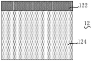
- an image sensor 10 of an embodiment of the present invention includes a pixel array 12 and a control circuit 14.
- the pixel array 12 includes a light sensitive region 122 and an imaging region 124.
- the light sensitive area 122 is used to detect the light intensity
- the imaging area 124 is used to acquire an image.
- the control circuit 14 is configured to receive a first command to control the light sensitive area 122 to detect the light intensity
- the control circuit 14 is configured to receive the second command to control the imaging area 124 to acquire an image
- the control circuit 14 can simultaneously receive the first instruction and the second instruction.
- the image sensor 10 of the embodiment of the present invention can be applied to the camera module 100 of the embodiment of the present invention.
- the camera module 100 includes an image sensor 10 and a filter 20.
- the filter 20 is disposed corresponding to the imaging area 124, and the light L passes through the filter 20 to reach the imaging area 124.
- the camera module 100 of the embodiment of the present invention can be applied to the electronic device 1000 of the embodiment of the present invention.
- the electronic device 1000 includes a camera module 100 and a processor 200.
- the processor 200 is coupled to a control circuit 14 for generating a first instruction and a second instruction.
- the electronic device 1000 further includes a display screen 300 for displaying data information such as video, images, text, icons, and the like.
- the control circuit 14 can realize the function of detecting the illumination intensity and acquiring the image by controlling one pixel array 12, thereby avoiding simultaneously setting one imaging element and one light sensing element, thereby reducing
- the number of components which in turn increases the proportion of space used to arrange the display screen 300, increases the screen ratio of the electronic device 1000.
- the filter 20 can be an RBG filter, and the RGB filters can be arranged in a Bayer array such that the light L passes through the filter 20 and then acquires a color image through the imaging region 124.
- the camera module 100 further includes a visible filter 30.
- the visible filter 30 is disposed corresponding to the photosensitive region 122.
- the light L passes through the visible filter 30 and reaches the photosensitive region 122.
- the visible light portion of the light L reaches the light sensing region 122, and the light sensing region 122 can be used to detect the light intensity of the visible light, and avoid the invisible light in the light L, such as infrared light or ultraviolet light. Interference.
- the electronic device 1000 includes a single camera module 100, and the single camera module 100 is a front camera module 100a.
- the front camera module 100a and the display screen 300 are disposed on the front side 400 of the electronic device 1000.
- the front camera module 100a can be used to simultaneously detect the light intensity of the front side 400 and acquire an image opposite to the front side 400.
- the electronic device 1000 includes two camera modules 100.
- the two camera modules 100 are a front camera module 100a and a rear camera module 100b, and a front camera module.
- 100a and display screen 300 are disposed on the front side 400 of the electronic device 1000.
- the rear camera module 100b is disposed on the back surface 500 of the electronic device 1000, and the back surface 500 is opposite to the front surface 400.
- the front camera module 100a can be used to simultaneously detect the illumination intensity of the front side 400 to obtain the front illumination intensity and to acquire an image that is opposite the front side 400.
- the rear camera module 100b can be used to simultaneously detect the illumination intensity of the back side 500 to obtain a rear illumination intensity and to acquire an image opposite the back side 500.
- the processor 200 is further configured to use the front light intensity detected from the front camera module 100a, and the rear light intensity detected by the rear camera module 100b is selected to be larger.
- the final light intensity Taking the electronic device 1000 as a mobile phone as an example, the user may have a large difference in the light intensity between the front side 400 and the back side 500 of the electronic device 1000 in use, for example, the user may place the mobile phone face down on the desktop, etc., if only based on the front
- the front light intensity detected by the camera module 100a controls the display brightness of the display screen 300. At this time, the display screen 300 may be in a state of not displaying or displaying a very low brightness.
- the electronic device 1000 When the user suddenly picks up the electronic device 1000 and uses it, The electronic device 1000 needs to re-awake the display screen 300 or increase the brightness of the display screen 300 in a short time. When the user frequently picks up and puts down, the electronic device 1000 needs to consume more power in order to control the switching of the brightness of the display screen 300. many.
- the electronic device 1000 of the embodiment of the present invention can simultaneously detect the rear light intensity. When the user places the mobile phone face down on the desktop, the brightness of the display screen 300 can be displayed according to the brightness of the rear light intensity within a certain time range, when the user When the electronic device 1000 is picked up again, the display screen 300 does not need to switch the display brightness, and is convenient to use and saves electric energy.
- the electronic device 1000 can control the display brightness of the display screen 300 according to a larger one of the front light intensity and the rear light intensity.
- the back surface 500 may face the light source of the ceiling (such as a chandelier) or the like, so that the rear light intensity is greater than the front light intensity, and the electronic device 1000 can adjust according to the rear light intensity.
- the display brightness of the display screen 300 is more conducive to the user to see the display content and reduce the eye fatigue of the user.
- the electronic device 1000 can be an electronic device 1000 such as a mobile phone, a tablet computer, or a smart watch.
- the embodiment of the present invention will be described by taking the electronic device 1000 as a mobile phone as an example.
- the illumination intensity obtained by the image sensor 10 can be used as a basis for adjusting the display brightness of the display screen 300 of the electronic device 1000. For example, when the illumination intensity is large, the display brightness of the display screen 300 is increased, or the illumination intensity changes from a large value to less than a certain threshold. It is judged that the user is answering the call and turns off the display screen 300.
- the image acquired by the image sensor 10 may be displayed on the display screen 300 or stored in a storage medium of the electronic device 1000 for reading or dumping.
- the processor 200 is configured to generate a first instruction and a second instruction. Further, the processor 200 transmits the first instruction and the second instruction to the control circuit 14. Specifically, the processor 200 may separately generate and transmit the first instruction, or separately generate or transmit the second instruction, or simultaneously generate and transmit the first instruction and the second instruction.
- the first instruction and the second instruction may be generated by the processor 200 when receiving the input operation, and the input operation may be an operation input by the user or an input of an application environment, for example, in the mobile phone of the embodiment of the present invention, the first instruction and the first instruction
- the second instruction may be generated after the processor 200 receives the operation of the user touching or pressing the specified function key on the mobile phone.
- the first instruction and the second instruction may also be generated after the processor 200 reaches the predetermined time point according to the system time of the mobile phone.
- the control circuit 14 is capable of simultaneously receiving the first command and the second command, that is, the control circuit 14 is capable of simultaneously controlling the light sensitive region 122 to detect the illumination intensity and control the imaging region 124 to acquire the image.
- the control circuit 14 can also be used to separately receive the first command to control the light sensitive region 122 to detect the light intensity, or to separately receive the second command to control the imaging region 124 to acquire the image.
- the light sensing region 122 and the imaging region 124 may both be in an inoperative state.
- the pixel array 12 is composed of a plurality of pixels arranged in an array.
- the pixels located in the light sensing area 122 are used to detect the light intensity, and the pixels located in the imaging area 124 are used to acquire images, and each pixel can be obtained according to the arrival.
- the light intensity of the light of the pixel produces a corresponding amount of power.
- the control circuit 14 is electrically connected to each pixel, and the control circuit 14 acquires the electric quantity generated by the corresponding pixel according to the received first instruction or the second instruction, and further analyzes the amount of the electric quantity by the processor 200 to obtain the illumination of the light reaching the pixel.
- the intensity, or further, is further analyzed by the processor 200 to analyze the illumination intensity of the light reaching the plurality of pixels to obtain an image.
- the ratio of the area of imaging region 124 to the area of pixel array 12 is greater than or equal to 0.6, and/or the ratio of the area of photosensitive region 122 to the area of pixel array 12 is greater than or equal to 0.1.
- the ratio of the area of the imaging area 124 to the area of the pixel array 12 may be 0.6, 0.7, 0.77, 0.8, 0.9, etc.
- the ratio of the area of the photosensitive area 122 to the area of the pixel array 12 may be 0.1, 0.2, 0.22. , 0.4, etc. In this way, the image sensor 10 is ensured to have a better imaging effect on the basis of the function of detecting the illumination intensity.
- the imaging zone 124 is continuously distributed and located at an intermediate position of the pixel array 12 , and the light sensing zone 122 is located at a peripheral location of the imaging zone 124 .
- the continuously distributed imaging zone 124 facilitates the formation of a continuous, complete image.
- the center of the imaging region 124 may coincide with the center of the pixel array 12, the imaging region 124 may be in a centrally symmetrical shape, and the light sensing region 122 may be located on one or more sides of the imaging region 124.
- the light-sensitive region 122 includes a plurality of sub-light-sensing regions 1221 having equal and spaced intervals.
- the illumination intensity finally detected by the light-sensing area 122 needs to comprehensively consider the illumination intensity detected by all the pixel points in the light-sensing area 122. Therefore, in order to obtain a more objective ambient light intensity, the light-sensitive area 122 can be dispersed as much as possible. That is, the photosensitive region 122 can be dispersed into a plurality of spaced sub-light sensing regions 1221.
- the plurality of sub-photosensitive regions 1221 are spaced apart to increase the detection range of the photosensitive region 122 while improving the accuracy of the detection of the photosensitive region 122.
- the number of sub-photosensitive regions 1221 is four, the ratio of the area of each sub-photosensitive region 1221 to the pixel array 12 may be 0.05, and the plurality of sub-photosensitive regions 1221 may be respectively distributed on the imaging region 124. Side, bottom, left and right.
- the specific number and location of the sub-photosensitive regions 1221 are not limited to the discussion of the above embodiments.
- the sub-light sensing region 1221 includes a left light sensing region 1222 and a right light sensing region 1223 .
- the left light sensing area 1222 is located on the left side of the imaging area 124
- the right light sensing area 1223 is located on the right side of the imaging area 124
- the left light sensing area 1222 and the right light sensing area 1223 are symmetrically distributed
- the left light sensing area 1222 detects the left light intensity, right.
- the light-sensing area 1223 detects the right light intensity
- the light-sensing area 122 detects the light intensity as the average of the left light intensity and the right light intensity.
- the left light sensing region 1222 and the right light sensing region 1223 have substantially the same effect on the light intensity ultimately detected by the light sensing region 122, and the light sensing region 122 is prevented from being too sensitive to light changes on the left or right side of the imaging region 124. The overall test results are inaccurate.
- the sub-photosensitive region 1221 includes a glare zone 1224 and a lower sensation zone 1225.
- the upper photosensitive region 1224 is located on the upper side of the imaging region 124
- the lower photosensitive region 1225 is located on the lower side of the imaging region 124
- the upper photosensitive region 1224 is symmetrically distributed with the lower photosensitive region 1225
- the upper photosensitive region 1224 detects the upper light intensity
- the light-sensing area 1225 detects the light intensity
- the light intensity detected by the light-sensitive area 122 is the average of the upper light intensity and the lower light intensity.
- the effects of the light-sensing region 1224 and the lower light-sensing region 1225 on the illumination intensity ultimately detected by the light-sensitive region 122 are substantially the same, and the light-sensitive region 122 is prevented from being too sensitive to light changes on the upper or lower side of the imaging region 124. The overall test results are inaccurate.
- the sub-light sensing region 1221 includes the left light sensing region 1222, the right light sensing region 1223, the upper light sensing region 1224, and the lower light sensing region 1225, and the left light sensing region 1222 and the right light sensing region. 1223 is symmetrically distributed, and the glazing area 1224 is symmetric with the lower light sensing area 1225.
- the left light sensing area 1222, the right light sensing area 1223, the upper light sensing area 1224 and the lower light sensing area 1225 are symmetrically distributed in the center, left.
- the light-sensing area 1222 detects the left light intensity
- the right light-sensitive area 1223 detects the right light intensity
- the upper light-sensing area 1224 detects the upper light intensity
- the lower light-sensitive area 1225 detects the lower light intensity
- the light-sensing area 122 detects the obtained light intensity.
- the light intensity is the mean of left light intensity, right light intensity, upper light intensity, and lower light intensity.
- the left light sensing region 1222, the right light sensing region 1223, the upper light sensing region 1224, and the lower light sensing region 1225 have substantially the same influence on the light intensity finally detected by the light sensing region 122, and the light sensing region 122 is prevented from being imaged.
- the light changes on the left, right, upper or lower side of 124 are too sensitive, resulting in inaccurate overall detection results.
- the above symmetric distribution refers to that both the area and the shape are symmetrically distributed and both are symmetric about the imaging area 124.
- the pixel array 12 is circular or elliptical, and the imaging area 124 is in a rectangular shape inscribed with the pixel array 12, and the circular or elliptical shape is removed from the inscribed rectangle.
- the area is the light sensitive area 122.
- the imaging region 124 is in the middle of the pixel array 12, and the image is easily acquired.
- the light-sensitive region 122 is relatively dispersed.
- the left side of the imaging region 124 is symmetric with the right-side light-sensing region 122, and the light-sensitive region 122 is opposite to the imaging region 124.
- the light changes on the left side and the right side are the same, while the upper side of the imaging area 124 is symmetrical with the light sensitive area 122 on the lower side, and the light sensitive area 122 is sensitive to the change of the light on the upper side and the lower side of the imaging area 124.
- the detection result of the light sensing area 122 is relatively accurate.
- the pixel array 12 has a rectangular shape
- the imaging area 124 has a circular or elliptical shape inscribed with a rectangle.
- the area except the inscribed circular or elliptical shape of the rectangle is the photosensitive area 122.
- the shape of the imaging area 124 is circular or elliptical, and the user can directly obtain a circular or elliptical picture through the imaging area 124, thereby eliminating the need for processing the photo in the later stage to meet the individual needs of the user.
- the light sensing area 122 is more dispersed, and the accuracy of the light intensity detected by the light sensing area 122 is improved.
- the imaging region 124 is at an intermediate position of the pixel array 12, and the image is easily acquired while being symmetric with the light sensing region 122 on the lower side of the imaging region 124, and the light sensing region 122 on the left and right sides of the imaging region 124. symmetry.
- the imaging regions 124 are continuously distributed, the light sensing regions 122 are continuously distributed, and the imaging regions 124 and the light sensing regions 122 are separated by a straight line.
- the structure of the pixel array 12 is simple, and the control circuit 14 can easily locate the pixels of the corresponding imaging area 124 or the light sensing area 122 after receiving the first instruction or the second instruction.
- the ratio of the area of the imaging region 124 to the area of the pixel array 12 is 0.8
- the ratio of the area of the photosensitive region 122 to the area of the pixel array 12 is 0.2.
- the imaging area 124 may be rectangular, such that the imaging area 124 acquires a rectangular image, and the light sensing area 122 may also be rectangular.
- the long side of the light sensing area 122 may intersect the long side of the imaging area 124 or the length of the photosensitive area 122.
- the edges intersect the short sides of the imaging zone 124.
- first and second are used for descriptive purposes only and are not to be construed as indicating or implying a relative importance or implicitly indicating the number of technical features indicated.
- features defining “first” or “second” may include at least one of the features, either explicitly or implicitly.
- the meaning of "a plurality” is at least two, such as two, three, etc., unless specifically defined otherwise.
- a "computer-readable medium” can be any apparatus that can contain, store, communicate, propagate, or transport a program for use in an instruction execution system, apparatus, or device, or in conjunction with such an instruction execution system, apparatus, or device.
- computer readable media include the following: electrical connections (electronic devices) having one or more wires, portable computer disk cartridges (magnetic devices), random access memory (RAM), Read only memory (ROM), erasable editable read only memory (EPROM or flash memory), fiber optic devices, and portable compact disk read only memory (CDROM).
- the computer readable medium may even be a paper or other suitable medium on which the program can be printed, as it may be optically scanned, for example by paper or other medium, followed by editing, interpretation or, if appropriate, other suitable The method is processed to obtain the program electronically and then stored in computer memory.
- portions of the invention may be implemented in hardware, software, firmware or a combination thereof.
- multiple steps or methods may be implemented in software or firmware stored in a memory and executed by a suitable instruction execution system.
- a suitable instruction execution system For example, if implemented in hardware, as in another embodiment, it can be implemented by any one or combination of the following techniques well known in the art: having logic gates for implementing logic functions on data signals. Discrete logic circuits, application specific integrated circuits with suitable combinational logic gates, programmable gate arrays (PGAs), field programmable gate arrays (FPGAs), etc.
- each functional unit in each embodiment of the present invention may be integrated into one processing module, or each unit may exist physically separately, or two or more units may be integrated into one module.
- the above integrated modules can be implemented in the form of hardware or in the form of software functional modules.
- the integrated modules, if implemented in the form of software functional modules and sold or used as stand-alone products, may also be stored in a computer readable storage medium.
- the above mentioned storage medium may be a read only memory, a magnetic disk or an optical disk or the like.
Landscapes
- Engineering & Computer Science (AREA)
- Signal Processing (AREA)
- Multimedia (AREA)
- Studio Devices (AREA)
Abstract
本发明公开了一种影像传感器(10)、相机模组(100)和电子装置(1000)。影像传感器(10)包括像素阵列(12)和控制电路(14)。像素阵列(12)包括光感区(122)和成像区(124),光感区(122)用于检测光照强度,成像区(124)用于获取影像。控制电路(14)用于接收第一指令以控制光感区(122)检测光照强度,控制电路(14)用于接收第二指令以控制成像区(124)获取影像。控制电路(14)能够同时接收第一指令和第二指令。
Description
优先权信息
本申请请求2017年05月03日向中国国家知识产权局提交的、专利申请号为201710305890.0的专利申请的优先权和权益,并且通过参照将其全文并入此处。
本发明涉及电子设备技术领域,更具体而言,涉及一种影像传感器、相机模组和电子装置。
通常可以在手机上设置前置摄像头以实现自拍的目的,且同时设置光感器,以实现依据环境光亮度调节手机屏幕显示亮度的目的,然而,同时布置前置摄像头和光感器需要占用的空间较大,导致手机中可用于布置显示屏的空间的比例较小,手机屏占比低。
发明内容
本发明的实施方式提供了一种影像传感器、相机模组和电子装置。
本发明实施方式的影像传感器包括:
像素阵列,所述像素阵列包括光感区和成像区,所述光感区用于检测光照强度,所述成像区用于获取影像;和
控制电路,所述控制电路用于接收第一指令以控制所述光感区检测光照强度,且所述控制电路用于接收第二指令以控制所述成像区获取影像,所述控制电路能够同时接收所述第一指令和所述第二指令。
在某些实施方式中,所述成像区连续分布且位于所述像素阵列的中间位置,所述光感区位于所述成像区的周缘位置。
在某些实施方式中,所述光感区包括多个子光感区,所述多个子光感区的面积相等且间隔设置。
在某些实施方式中,所述子光感区包括位于所述成像区左侧的左光感区和位于所述成像区右侧的右光感区,所述左光感区与所述右光感区对称分布,所述左光感区检测得到左光照强度,所述右光感区检测得到右光照强度,所述光感区检测得到的光照强度为所述左光照强度和所述右光照强度的均值;或
所述子光感区包括位于所述成像区上侧的上光感区和位于所述成像区下侧的下光感区,所述上光感区与所述下光感区对称分布,所述上光感区检测得到上光照强度,所述下 光感区检测得到下光照强度,所述光感区检测得到的光照强度为所述上光照强度和所述下光照强度的均值;或
所述子光感区包括分别位于所述成像区左侧、右侧、上侧和下侧的左光感区、右光感区、上光感区和下光感区,所述左光感区与所述右光感区对称分布,所述上光感区与所述下光感区对称分布,所述左光感区检测得到左光照强度,所述右光感区检测得到右光照强度,所述上光感区检测得到上光照强度,所述下光感区检测得到下光照强度,所述光感区检测得到的光照强度为所述左光照强度、所述右光照强度、所述上光照强度和所述下光照强度的均值。
在某些实施方式中,所述像素阵列呈圆形或椭圆形,所述成像区呈与所述像素阵列内接的矩形,所述圆形或所述椭圆形除去所述内接的矩形之外的区域为所述光感区;或
所述像素阵列呈矩形,所述成像区呈与所述矩形内接的圆形或椭圆形,所述矩形除去所述内接的圆形或椭圆形之外的区域为所述光感区。
在某些实施方式中,所述成像区连续分布,所述光感区连续分布,所述成像区与所述光感区由一直线分割。
在某些实施方式中,所述成像区的面积与所述像素阵列的面积的比值大于或等于0.6,和/或
所述光感区的面积与所述像素阵列的面积的比值大于或等于0.1。
本发明实施方式的相机模组包括:
上述任一实施方式所述的影像传感器;和
与所述成像区对应设置的滤光片,光线穿过所述滤光片后到达所述成像区。
本发明实施方式的电子装置包括:
上述实施方式所述的相机模组;和
与所述控制电路连接的处理器,所述处理器用于生成所述第一指令和所述第二指令。
在某些实施方式中,所述相机模组的数量为两个,其中一个所述相机模组为前置相机模组,另一个所述相机模组为后置相机模组,所述前置相机模组的光感区检测光照强度以得到前置光照强度,所述后置相机模组的光感区检测光照强度以得到后置光照强度,所述处理器还用于从所述前置光照强度和所述后置光照强度中选取较大者以作为最终光照强度。
上述的影像传感器、相机模组和电子装置中,控制电路通过控制一个像素阵列就可实现检测光照强度和获取影像的功能,避免同时设置一个摄像元件及一个光感元件,减少了元器件的数量,进而可增加用于布置显示屏的空间的比例,提高电子装置的屏占比。
本发明的实施方式的附加方面和优点将在下面的描述中部分给出,部分将从下面的描 述中变得明显,或通过本发明的实施方式的实践了解到。
本发明的上述和/或附加的方面和优点从结合下面附图对实施方式的描述中将变得明显和容易理解,其中:
图1是本发明实施方式的电子装置的立体示意图;
图2是本发明实施方式的电子装置的侧视图;
图3是本发明实施方式的相机模组的结构示意图;
图4是本发明实施方式的像素阵列的平面示意图;
图5是本发明实施方式的像素阵列的平面示意图;
图6是本发明实施方式的像素阵列的平面示意图;
图7是本发明实施方式的像素阵列的平面示意图;
图8是本发明实施方式的像素阵列的平面示意图;
图9是本发明实施方式的像素阵列的平面示意图;
图10是本发明实施方式的像素阵列的平面示意图;
图11是本发明实施方式的像素阵列的平面示意图;
图12是本发明实施方式的像素阵列的平面示意图。
主要元件符号说明:
电子装置1000、相机模组100、前置相机模组100a、后置相机模组100b、影像传感器10、像素阵列12、光感区122、子光感区1221、左光感区1222、右光感区1223、上光感区1224、下光感区1225、成像区124、控制电路14、滤光片20、可见滤光片30、处理器200、显示屏300、正面400、背面500。
以下结合附图对本发明的实施方式作进一步说明。附图中相同或类似的标号自始至终表示相同或类似的元件或具有相同或类似功能的元件。
另外,下面结合附图描述的本发明的实施方式是示例性的,仅用于解释本发明的实施方式,而不能理解为对本发明的限制。
在本发明中,除非另有明确的规定和限定,第一特征在第二特征“上”或“下”可以是第一和第二特征直接接触,或第一和第二特征通过中间媒介间接接触。而且,第一特征在第二特征“之上”、“上方”和“上面”可是第一特征在第二特征正上方或斜上方,或仅 仅表示第一特征水平高度高于第二特征。第一特征在第二特征“之下”、“下方”和“下面”可以是第一特征在第二特征正下方或斜下方,或仅仅表示第一特征水平高度小于第二特征。
请参阅图1-3,本发明实施方式的影像传感器10包括像素阵列12和控制电路14。像素阵列12包括光感区122和成像区124。光感区122用于检测光照强度,成像区124用于获取影像。控制电路14用于接收第一指令以控制光感区122检测光照强度,控制电路14用于接收第二指令以控制成像区124获取影像,控制电路14能够同时接收第一指令和第二指令。
本发明实施方式的影像传感器10可应用到本发明实施方式的相机模组100中,相机模组100包括影像传感器10和滤光片20。滤光片20与成像区124对应设置,光线L穿过滤光片20后到达成像区124。
本发明实施方式的相机模组100可应用到本发明实施方式的电子装置1000中,电子装置1000包括相机模组100和处理器200。处理器200与控制电路14连接,处理器200用于生成第一指令和第二指令。在某些实施方式中,电子装置1000还包括显示屏300,显示屏300用于显示视频、图像、文本、图标等数据信息。
上述的影像传感器10、相机模组100和电子装置1000中,控制电路14通过控制一个像素阵列12就可实现检测光照强度和获取影像的功能,避免同时设置一个摄像元件及一个光感元件,减少了元器件的数量,进而可增加用于布置显示屏300的空间的比例,提高电子装置1000的屏占比。
在某些实施方式中,滤光片20可以是RBG滤光片,RGB滤光片可以以拜尔阵列排列,以使得光线L穿过滤光片20后再通过成像区124获取彩色的影像。进一步地,在某些实施方式中,相机模组100还包括可见滤光片30,可见滤光片30与光感区122对应设置,光线L穿过可见滤光片30后到达光感区122,如此,光线L经过可见滤光片30后,光线L中的可见光部分到达光感区122,光感区122可用于检测可见光的光照强度,避免光线L中不可见光,例如红外光、紫外光的干扰。
在某些实施方式中,电子装置1000包括单个相机模组100,单个相机模组100为前置相机模组100a。前置相机模组100a与显示屏300设置在电子装置1000的正面400,前置相机模组100a可用于同时检测正面400的光照强度和获取与正面400相对的影像。
请再结合图3,在某些实施方式中,电子装置1000包括两个相机模组100,两个相机模组100为前置相机模组100a和后置相机模组100b,前置相机模组100a与显示屏300设置在电子装置1000的正面400,后置相机模组100b设置在电子装置1000的背面500,背面500与正面400相背。前置相机模组100a可用于同时检测正面400的光照强度以得到前置光照强度和获取与正面400相对的影像。后置相机模组100b可用于同时检测背面500的 光照强度以得到后置光照强度和获取与背面500相对的影像。
如此,在电子装置1000的使用过程中,处理器200还用于从前置相机模组100a检测得到的前置光照强度,和后置相机模组100b检测得到的后置光照强度中选取较大者作为最终光照强度。以电子装置1000为手机为例,用户在使用中可能存在电子装置1000的正面400与背面500的光照强度相差较大的情况,例如用户可能将手机正面朝下放在桌面上等,如果仅仅依据前置相机模组100a检测得到的前置光照强度控制显示屏300的显示亮度,此时显示屏300可能处于不显示或者显示亮度极低的状态,当用户突然重新拿起电子装置1000并使用时,电子装置1000需要重新唤醒显示屏300或者将显示屏300的亮度在短时间内调高,当用户频繁拿起和放下时,电子装置1000为了控制显示屏300亮度的切换的操作需要耗费的电能较多。本发明实施方式的电子装置1000可同时检测后置光照强度,当用户将手机正面朝下放置在桌面上时,显示屏300亮度在一定时间范围内可依据后置光照强度的亮度显示,当用户重新拿起电子装置1000使用时,显示屏300无需要切换显示亮度,使用方便且节约电能。
在另一个实施例中,电子装置1000可依据前置光照强度和后置光照强度中的较大的一个来控制显示屏300的显示亮度。例如当用户在室内平躺操作电子装置1000时,背面500可能朝向天花板的光源(如吊灯)等而使得后置光照强度大于前置光照强度,此时电子装置1000可依据后置光照强度来调节显示屏300的显示亮度,更有利于用户看清显示内容,减少用户用眼疲劳。
电子装置1000可以是手机、平板电脑、智能手表等电子装置1000。本发明实施方式以电子装置1000为手机为例进行说明。影像传感器10获取的光照强度可作为调整电子装置1000显示屏300的显示亮度的依据,例如在光照强度较大时增大显示屏300的显示亮度、或者光照强度从较大变化为小于某一阈值时判断用户正在接听电话并关闭显示屏300。影像传感器10获取的影像可在显示屏300中显示,或者存储在电子装置1000的存储介质中以便于读取或转存。
处理器200用于生成第一指令和第二指令,进一步地,处理器200将第一指令和第二指令发送给控制电路14。具体地,处理器200可以单独生成并发送第一指令,或者单独生成或发送第二指令,或者同时生成并发送第一指令和第二指令。第一指令和第二指令可以是处理器200在接收到输入操作时生成,输入操作可以是用户输入的操作或者是应用环境的输入,例如在本发明实施例的手机中,第一指令和第二指令可以是处理器200接收到用户在手机上触摸或按压指定功能键的操作后生成,第一指令和第二指令也可以是处理器200依据手机的系统时间到达预定的时间点后生成。
控制电路14能够同时接收第一指令和第二指令,也就是说,控制电路14能够同时控 制光感区122检测光照强度和控制成像区124获取影像。当然,控制电路14也能用于单独接收第一指令以控制光感区122检测光照强度,或者单独接收第二指令以控制成像区124获取影像。当控制电路14未接收到第一指令和第二指令时,光感区122和成像区124可均处于不工作的状态。具体地,像素阵列12由多个呈阵列排布的像素组成,位于光感区122内的像素用于检测光照强度,位于成像区124内的像素用于获取图像,每个像素均可依据到达像素的光线的光照强度产生相应的电量。
控制电路14与每个像素电连接,控制电路14依据接收到的第一指令或第二指令获取由对应的像素产生的电量,并进一步通过处理器200分析电量的大小得到到达像素的光线的光照强度,或者进一步通过处理器200综合分析到达多个像素的光线的光照强度以得到影像。
在某些实施方式中,成像区124的面积与像素阵列12的面积的比值大于或等于0.6,和/或光感区122的面积与像素阵列12的面积的比值大于或等于0.1。具体地,成像区124的面积与像素阵列12的面积的比值可以是0.6、0.7、0.77、0.8、0.9等,光感区122的面积与像素阵列12的面积的比值可以是0.1、0.2、0.22、0.4等。如此,保证影像传感器10在具有检测光照强度的功能的基础上,具有较好的成像效果。
请参阅图4和图5,在某些实施方式中,成像区124连续分布且位于像素阵列12的中间位置,光感区122位于成像区124的周缘位置。如此,连续分布的成像区124便于形成连续的、完整的影像。具体地,成像区124的中心可以与像素阵列12的中心重合,成像区124可以是呈中心对称的形状,光感区122可以位于成像区124的一侧或者多侧。
在某些实施方式中,光感区122包括多个子光感区1221,多个子光感区1221的面积相等且间隔设置。
可以理解,光感区122最终检测的光照强度需要综合考虑光感区122内所有像素点检测得到的光照强度,因此,为了得到较为客观的环境光照强度,可以尽可能地将光感区122分散,也就是说,可以将光感区122分散为多个间隔的子光感区1221。
如此,多个子光感区1221间隔设置可扩大光感区122的检测范围同时提高光感区122检测的准确性。在一个实施例中,子光感区1221的数量为四个,每个子光感区1221的面积与像素阵列12的比值可以是0.05,多个子光感区1221可以分别分布在成像区124的上侧、下侧、左侧和右侧。当然,子光感区1221的具体数量和位置不限于上述实施例的讨论。
具体地,请参阅图6,在某些实施方式中,子光感区1221包括左光感区1222和右光感区1223。左光感区1222位于成像区124左侧,右光感区1223位于成像区124右侧,左光感区1222与右光感区1223对称分布,左光感区1222检测得到左光照强度,右光感区1223检测得到右光照强度,光感区122检测得到的光照强度为左光照强度和右光照强度的 均值。
如此,左光感区1222和右光感区1223对最终由光感区122检测到的光照强度的影响基本相同,避免光感区122对成像区124左侧或右侧的光线变化过于敏感而导致整体的检测结果不准确。
在某些实施方式中,子光感区1221包括上光感区1224和下光感区1225。上光感区1224位于成像区124上侧,下光感区1225位于成像区124下侧,上光感区1224与下光感区1225对称分布,上光感区1224检测得到上光照强度,下光感区1225检测得到下光照强度,光感区122检测得到的光照强度为上光照强度和下光照强度的均值。
如此,上光感区1224和下光感区1225对最终由光感区122检测到的光照强度的影响基本相同,避免光感区122对成像区124上侧或下侧的光线变化过于敏感而导致整体的检测结果不准确。
在某些实施方式中,子光感区1221同时包括上述的左光感区1222、右光感区1223、上光感区1224和下光感区1225,左光感区1222与右光感区1223对称分布,上光感区1224与下光感区1225对称,较佳地,左光感区1222、右光感区1223、上光感区1224和下光感区1225呈中心对称分布,左光感区1222检测得到左光照强度,右光感区1223检测得到右光照强度,上光感区1224检测得到上光照强度,下光感区1225检测得到下光照强度,光感区122检测得到的光照强度为左光照强度、右光照强度、上光照强度和下光照强度的均值。
如此,左光感区1222、右光感区1223、上光感区1224和下光感区1225对最终由光感区122检测到的光照强度的影响基本相同,避免光感区122对成像区124左侧、右侧、上侧或下侧的光线变化过于敏感而导致整体的检测结果不准确。
需要说明的是,上述对称分布指的是面积和形状均对称分布且均是关于成像区124对称。
请参阅图7和图8,在某些实施方式中,像素阵列12呈圆形或椭圆形,成像区124呈与像素阵列12内接的矩形,圆形或椭圆形除去内接的矩形之外的区域为光感区122。
如此,成像区124处于像素阵列12的中间位置,易于获取影像,光感区122较分散,在成像区124的左侧与右侧的光感区122对称,光感区122对成像区124的左侧与右侧的光线变化敏感程度相同,同时在成像区124的上侧与下侧的光感区122对称,光感区122对成像区124的上侧与下侧的光线变化敏感程度相同,光感区122的检测结果较准确。
请参阅图9和图10,像素阵列12呈矩形,成像区124呈与矩形内接的圆形或椭圆形,矩形除去内接的圆形或椭圆形之外的区域为光感区122。
如此,成像区124的形状呈圆形或椭圆形,用户可直接通过成像区124获取圆形或椭 圆形的图片而省去后期对照片进行处理的操作,满足用户的个性化需求。同时光感区122较分散,提高光感区122检测得到的光照强度的准确性。
如此,成像区124处于像素阵列12的中间位置,易于获取影像,同时在成像区124的上侧与下侧的光感区122对称,在成像区124的左侧与右侧的光感区122对称。
请参阅图11和图12,在某些实施方式中,成像区124连续分布,光感区122连续分布,成像区124与光感区122由一直线分割。如此,像素阵列12的结构简单,控制电路14接收到第一指令或第二指令后容易定位到对应的成像区124或光感区122的像素。具体地,在一个实施例中,成像区124的面积与像素阵列12的面积的比值为0.8,光感区122的面积与像素阵列12的面积的比值为0.2。成像区124可以呈矩形,以使得成像区124获取呈矩形的影像,光感区122也可以呈矩形,光感区122的长边可以与成像区124的长边相交或者光感区122的长边与成像区124的短边相交。
在本说明书的描述中,参考术语“一个实施例”、“一些实施例”、“示例”、“具体示例”、或“一些示例”等的描述意指结合该实施例或示例描述的具体特征、结构、材料或者特点包含于本发明的至少一个实施例或示例中。在本说明书中,对上述术语的示意性表述不必须针对的是相同的实施例或示例。而且,描述的具体特征、结构、材料或者特点可以在任一个或多个实施例或示例中以合适的方式结合。此外,在不相互矛盾的情况下,本领域的技术人员可以将本说明书中描述的不同实施例或示例以及不同实施例或示例的特征进行结合和组合。
此外,术语“第一”、“第二”仅用于描述目的,而不能理解为指示或暗示相对重要性或者隐含指明所指示的技术特征的数量。由此,限定有“第一”、“第二”的特征可以明示或者隐含地包括至少一个该特征。在本发明的描述中,“多个”的含义是至少两个,例如两个,三个等,除非另有明确具体的限定。
流程图中或在此以其他方式描述的任何过程或方法描述可以被理解为,表示包括一个或更多个用于实现特定逻辑功能或过程的步骤的可执行指令的代码的模块、片段或部分,并且本发明的优选实施方式的范围包括另外的实现,其中可以不按所示出或讨论的顺序,包括根据所涉及的功能按基本同时的方式或按相反的顺序,来执行功能,这应被本发明的实施例所属技术领域的技术人员所理解。
在流程图中表示或在此以其他方式描述的逻辑和/或步骤,例如,可以被认为是用于实现逻辑功能的可执行指令的定序列表,可以具体实现在任何计算机可读介质中,以供指令执行系统、装置或设备(如基于计算机的系统、包括处理器的系统或其他可以从指令执行系统、装置或设备取指令并执行指令的系统)使用,或结合这些指令执行系统、装置或设备而使用。就本说明书而言,"计算机可读介质"可以是任何可以包含、存储、通信、传播 或传输程序以供指令执行系统、装置或设备或结合这些指令执行系统、装置或设备而使用的装置。计算机可读介质的更具体的示例(非穷尽性列表)包括以下:具有一个或多个布线的电连接部(电子装置),便携式计算机盘盒(磁装置),随机存取存储器(RAM),只读存储器(ROM),可擦除可编辑只读存储器(EPROM或闪速存储器),光纤装置,以及便携式光盘只读存储器(CDROM)。另外,计算机可读介质甚至可以是可在其上打印所述程序的纸或其他合适的介质,因为可以例如通过对纸或其他介质进行光学扫描,接着进行编辑、解译或必要时以其他合适方式进行处理来以电子方式获得所述程序,然后将其存储在计算机存储器中。
应当理解,本发明的各部分可以用硬件、软件、固件或它们的组合来实现。在上述实施方式中,多个步骤或方法可以用存储在存储器中且由合适的指令执行系统执行的软件或固件来实现。例如,如果用硬件来实现,和在另一实施方式中一样,可用本领域公知的下列技术中的任一项或他们的组合来实现:具有用于对数据信号实现逻辑功能的逻辑门电路的离散逻辑电路,具有合适的组合逻辑门电路的专用集成电路,可编程门阵列(PGA),现场可编程门阵列(FPGA)等。
本技术领域的普通技术人员可以理解实现上述实施例方法携带的全部或部分步骤是可以通过程序来指令相关的硬件完成,所述的程序可以存储于一种计算机可读存储介质中,该程序在执行时,包括方法实施例的步骤之一或其组合。
此外,在本发明各个实施例中的各功能单元可以集成在一个处理模块中,也可以是各个单元单独物理存在,也可以两个或两个以上单元集成在一个模块中。上述集成的模块既可以采用硬件的形式实现,也可以采用软件功能模块的形式实现。所述集成的模块如果以软件功能模块的形式实现并作为独立的产品销售或使用时,也可以存储在一个计算机可读取存储介质中。
上述提到的存储介质可以是只读存储器,磁盘或光盘等。尽管上面已经示出和描述了本发明的实施例,可以理解的是,上述实施例是示例性的,不能理解为对本发明的限制,本领域的普通技术人员在本发明的范围内可以对上述实施例进行变化、修改、替换和变型。
Claims (10)
- 一种影像传感器,其特征在于,包括:像素阵列,所述像素阵列包括光感区和成像区,所述光感区用于检测光照强度,所述成像区用于获取影像;和控制电路,所述控制电路用于接收第一指令以控制所述光感区检测光照强度,且所述控制电路用于接收第二指令以控制所述成像区获取影像,所述控制电路能够同时接收所述第一指令和所述第二指令。
- 根据权利要求1所述的影像传感器,其特征在于,所述成像区连续分布且位于所述像素阵列的中间位置,所述光感区位于所述成像区的周缘位置。
- 根据权利要求2所述的影像传感器,其特征在于,所述光感区包括多个子光感区,所述多个子光感区的面积相等且间隔设置。
- 根据权利要求3所述的影像传感器,其特征在于,所述子光感区包括位于所述成像区左侧的左光感区和位于所述成像区右侧的右光感区,所述左光感区与所述右光感区对称分布,所述左光感区检测得到左光照强度,所述右光感区检测得到右光照强度,所述光感区检测得到的光照强度为所述左光照强度和所述右光照强度的均值;或所述子光感区包括位于所述成像区上侧的上光感区和位于所述成像区下侧的下光感区,所述上光感区与所述下光感区对称分布,所述上光感区检测得到上光照强度,所述下光感区检测得到下光照强度,所述光感区检测得到的光照强度为所述上光照强度和所述下光照强度的均值;或所述子光感区包括分别位于所述成像区左侧、右侧、上侧和下侧的左光感区、右光感区、上光感区和下光感区,所述左光感区与所述右光感区对称分布,所述上光感区与所述下光感区对称分布,所述左光感区检测得到左光照强度,所述右光感区检测得到右光照强度,所述上光感区检测得到上光照强度,所述下光感区检测得到下光照强度,所述光感区检测得到的光照强度为所述左光照强度、所述右光照强度、所述上光照强度和所述下光照强度的均值。
- 根据权利要求1所述的影像传感器,其特征在于,所述像素阵列呈圆形或椭圆形,所述成像区呈与所述像素阵列内接的矩形,所述圆形或所述椭圆形除去所述内接的矩形之外的区域为所述光感区;或所述像素阵列呈矩形,所述成像区呈与所述矩形内接的圆形或椭圆形,所述矩形除去所述内接的圆形或椭圆形之外的区域为所述光感区。
- 根据权利要求1所述的影像传感器,其特征在于,所述成像区连续分布,所述光感区连续分布,所述成像区与所述光感区由一直线分割。
- 根据权利要求1-6任意一项所述的影像传感器,其特征在于,所述成像区的面积与所述像素阵列的面积的比值大于或等于0.6,和/或所述光感区的面积与所述像素阵列的面积的比值大于或等于0.1。
- 一种相机模组,其特征在于,包括:权利要求1-7任意一项所述的影像传感器;和与所述成像区对应设置的滤光片,光线穿过所述滤光片后到达所述成像区。
- 一种电子装置,其特征在于,包括:权利要求8所述的相机模组;和与所述控制电路连接的处理器,所述处理器用于生成所述第一指令和所述第二指令。
- 根据权利要求9所述的电子装置,其特征在于,所述相机模组的数量为两个,其中一个所述相机模组为前置相机模组,另一个所述相机模组为后置相机模组,所述前置相机模组的光感区检测光照强度以得到前置光照强度,所述后置相机模组的光感区检测光照强度以得到后置光照强度,所述处理器还用于从所述前置光照强度和所述后置光照强度中选取较大者以作为最终光照强度。
Priority Applications (2)
| Application Number | Priority Date | Filing Date | Title |
|---|---|---|---|
| US16/603,766 US11310434B2 (en) | 2017-05-03 | 2018-04-13 | Image sensor for camera module of electronic device having a pixel array with an imaging area and a light sensing area |
| EP18793991.3A EP3606028B1 (en) | 2017-05-03 | 2018-04-13 | Image sensor, camera module, and electronic device |
Applications Claiming Priority (2)
| Application Number | Priority Date | Filing Date | Title |
|---|---|---|---|
| CN201710305890.0 | 2017-05-03 | ||
| CN201710305890.0A CN107222591B (zh) | 2017-05-03 | 2017-05-03 | 影像传感器、相机模组和电子装置 |
Publications (1)
| Publication Number | Publication Date |
|---|---|
| WO2018201876A1 true WO2018201876A1 (zh) | 2018-11-08 |
Family
ID=59944718
Family Applications (1)
| Application Number | Title | Priority Date | Filing Date |
|---|---|---|---|
| PCT/CN2018/083046 Ceased WO2018201876A1 (zh) | 2017-05-03 | 2018-04-13 | 影像传感器、相机模组和电子装置 |
Country Status (4)
| Country | Link |
|---|---|
| US (1) | US11310434B2 (zh) |
| EP (1) | EP3606028B1 (zh) |
| CN (1) | CN107222591B (zh) |
| WO (1) | WO2018201876A1 (zh) |
Cited By (1)
| Publication number | Priority date | Publication date | Assignee | Title |
|---|---|---|---|---|
| CN117373402A (zh) * | 2023-12-08 | 2024-01-09 | 深圳市华远显示器件有限公司 | 一种控制液晶显示屏显示方法及系统 |
Families Citing this family (8)
| Publication number | Priority date | Publication date | Assignee | Title |
|---|---|---|---|---|
| CN107426471B (zh) | 2017-05-03 | 2021-02-05 | Oppo广东移动通信有限公司 | 相机模组和电子装置 |
| CN107222591B (zh) | 2017-05-03 | 2021-02-05 | Oppo广东移动通信有限公司 | 影像传感器、相机模组和电子装置 |
| CN107249109B (zh) | 2017-05-03 | 2021-02-05 | Oppo广东移动通信有限公司 | 影像传感器、相机模组和电子装置 |
| US10983652B2 (en) * | 2018-04-13 | 2021-04-20 | Samsung Electronics Co., Ltd. | Display having opaque member disposed in area surrounded by pixels and electronic apparatus having the same |
| CN108600537A (zh) * | 2018-04-23 | 2018-09-28 | Oppo广东移动通信有限公司 | 接近传感器、人体遮挡判断方法、电子装置及可读存储介质 |
| CN109543558B (zh) * | 2018-10-30 | 2023-12-26 | Oppo广东移动通信有限公司 | 指纹图像处理方法及相关产品 |
| CN114125240A (zh) * | 2021-11-30 | 2022-03-01 | 维沃移动通信有限公司 | 图像传感器、摄像模组、电子设备及拍摄方法 |
| US12464207B2 (en) * | 2022-12-28 | 2025-11-04 | Motorola Solutions, Inc. | Image sensor with an integrated infrared cut-off filter |
Citations (8)
| Publication number | Priority date | Publication date | Assignee | Title |
|---|---|---|---|---|
| US20080316330A1 (en) * | 2007-06-22 | 2008-12-25 | Canon Kabushiki Kaisha | Image sensing apparatus and control method for same, and image sensing system |
| CN103973945A (zh) * | 2013-01-25 | 2014-08-06 | 三星电机株式会社 | 照相机模块 |
| CN104486987A (zh) * | 2012-07-26 | 2015-04-01 | 橄榄医疗公司 | 具有最小面积单片式cmos图像传感器的相机系统 |
| CN104519327A (zh) * | 2013-10-07 | 2015-04-15 | 联咏科技股份有限公司 | 图像传感器及图像采集系统 |
| CN107222591A (zh) * | 2017-05-03 | 2017-09-29 | 广东欧珀移动通信有限公司 | 影像传感器、相机模组和电子装置 |
| CN107249109A (zh) * | 2017-05-03 | 2017-10-13 | 广东欧珀移动通信有限公司 | 影像传感器、相机模组和电子装置 |
| CN107426470A (zh) * | 2017-05-03 | 2017-12-01 | 广东欧珀移动通信有限公司 | 相机模组和电子装置 |
| CN107426471A (zh) * | 2017-05-03 | 2017-12-01 | 广东欧珀移动通信有限公司 | 相机模组和电子装置 |
Family Cites Families (9)
| Publication number | Priority date | Publication date | Assignee | Title |
|---|---|---|---|---|
| CA2330433A1 (en) * | 2000-01-21 | 2001-07-21 | Symagery Microsystems Inc. | Smart exposure determination for imagers |
| US20080122821A1 (en) * | 2006-11-24 | 2008-05-29 | Sony Ericsson Mobile Communications Ab | Luminance control for a display |
| EP2472853A1 (en) * | 2011-01-03 | 2012-07-04 | STMicroelectronics (Grenoble 2) SAS | Imaging device with ambient light sensing means |
| CN102595030A (zh) * | 2011-01-12 | 2012-07-18 | 英属开曼群岛商恒景科技股份有限公司 | 具环境光感测的数字摄像装置 |
| US8735795B2 (en) * | 2012-01-20 | 2014-05-27 | Omnivision Technologies, Inc. | Image sensor with integrated ambient light detection |
| CN202798942U (zh) * | 2012-08-09 | 2013-03-13 | 广东欧珀移动通信有限公司 | 图像传感器及应用该图像传感器的摄像头和电子产品 |
| US20140168372A1 (en) * | 2012-12-17 | 2014-06-19 | Eminent Electronic Technology Corp. Ltd. | Sensing apparatus and sensing method for generating three-dimensional image information |
| US9277144B2 (en) * | 2014-03-12 | 2016-03-01 | Apple Inc. | System and method for estimating an ambient light condition using an image sensor and field-of-view compensation |
| US9692968B2 (en) * | 2014-07-31 | 2017-06-27 | Invisage Technologies, Inc. | Multi-mode power-efficient light and gesture sensing in image sensors |
-
2017
- 2017-05-03 CN CN201710305890.0A patent/CN107222591B/zh active Active
-
2018
- 2018-04-13 US US16/603,766 patent/US11310434B2/en active Active
- 2018-04-13 WO PCT/CN2018/083046 patent/WO2018201876A1/zh not_active Ceased
- 2018-04-13 EP EP18793991.3A patent/EP3606028B1/en active Active
Patent Citations (8)
| Publication number | Priority date | Publication date | Assignee | Title |
|---|---|---|---|---|
| US20080316330A1 (en) * | 2007-06-22 | 2008-12-25 | Canon Kabushiki Kaisha | Image sensing apparatus and control method for same, and image sensing system |
| CN104486987A (zh) * | 2012-07-26 | 2015-04-01 | 橄榄医疗公司 | 具有最小面积单片式cmos图像传感器的相机系统 |
| CN103973945A (zh) * | 2013-01-25 | 2014-08-06 | 三星电机株式会社 | 照相机模块 |
| CN104519327A (zh) * | 2013-10-07 | 2015-04-15 | 联咏科技股份有限公司 | 图像传感器及图像采集系统 |
| CN107222591A (zh) * | 2017-05-03 | 2017-09-29 | 广东欧珀移动通信有限公司 | 影像传感器、相机模组和电子装置 |
| CN107249109A (zh) * | 2017-05-03 | 2017-10-13 | 广东欧珀移动通信有限公司 | 影像传感器、相机模组和电子装置 |
| CN107426470A (zh) * | 2017-05-03 | 2017-12-01 | 广东欧珀移动通信有限公司 | 相机模组和电子装置 |
| CN107426471A (zh) * | 2017-05-03 | 2017-12-01 | 广东欧珀移动通信有限公司 | 相机模组和电子装置 |
Non-Patent Citations (1)
| Title |
|---|
| See also references of EP3606028A4 |
Cited By (2)
| Publication number | Priority date | Publication date | Assignee | Title |
|---|---|---|---|---|
| CN117373402A (zh) * | 2023-12-08 | 2024-01-09 | 深圳市华远显示器件有限公司 | 一种控制液晶显示屏显示方法及系统 |
| CN117373402B (zh) * | 2023-12-08 | 2024-02-20 | 深圳市华远显示器件有限公司 | 一种控制液晶显示屏显示方法及系统 |
Also Published As
| Publication number | Publication date |
|---|---|
| EP3606028B1 (en) | 2022-06-29 |
| US20210099629A1 (en) | 2021-04-01 |
| CN107222591B (zh) | 2021-02-05 |
| EP3606028A4 (en) | 2020-03-25 |
| US11310434B2 (en) | 2022-04-19 |
| EP3606028A1 (en) | 2020-02-05 |
| CN107222591A (zh) | 2017-09-29 |
Similar Documents
| Publication | Publication Date | Title |
|---|---|---|
| WO2018201876A1 (zh) | 影像传感器、相机模组和电子装置 | |
| AU2018263021B2 (en) | Camera assembly and mobile electronic device | |
| WO2018201875A1 (zh) | 影像传感器、相机模组和电子装置 | |
| AU2018263022B2 (en) | Camera assembly and mobile electronic device | |
| JP6801114B2 (ja) | カメラアセンブリ及び携帯電子機器 | |
| CN107135341B (zh) | 影像传感器、相机模组及电子装置 | |
| CN106155693A (zh) | 控制方法及控制装置 | |
| CN106201254A (zh) | 控制方法、控制装置及电子装置 | |
| HK1244139A1 (zh) | 相机模组及电子装置 | |
| HK1244140B (zh) | 相机模组及电子装置 |
Legal Events
| Date | Code | Title | Description |
|---|---|---|---|
| 121 | Ep: the epo has been informed by wipo that ep was designated in this application |
Ref document number: 18793991 Country of ref document: EP Kind code of ref document: A1 |
|
| NENP | Non-entry into the national phase |
Ref country code: DE |
|
| ENP | Entry into the national phase |
Ref document number: 2018793991 Country of ref document: EP Effective date: 20191030 |