WO2018216144A1 - 電力変換装置 - Google Patents
電力変換装置 Download PDFInfo
- Publication number
- WO2018216144A1 WO2018216144A1 PCT/JP2017/019386 JP2017019386W WO2018216144A1 WO 2018216144 A1 WO2018216144 A1 WO 2018216144A1 JP 2017019386 W JP2017019386 W JP 2017019386W WO 2018216144 A1 WO2018216144 A1 WO 2018216144A1
- Authority
- WO
- WIPO (PCT)
- Prior art keywords
- voltage
- margin
- load
- allowable
- upper limit
- Prior art date
- Legal status (The legal status is an assumption and is not a legal conclusion. Google has not performed a legal analysis and makes no representation as to the accuracy of the status listed.)
- Ceased
Links
Images


Classifications
-
- H—ELECTRICITY
- H02—GENERATION; CONVERSION OR DISTRIBUTION OF ELECTRIC POWER
- H02M—APPARATUS FOR CONVERSION BETWEEN AC AND AC, BETWEEN AC AND DC, OR BETWEEN DC AND DC, AND FOR USE WITH MAINS OR SIMILAR POWER SUPPLY SYSTEMS; CONVERSION OF DC OR AC INPUT POWER INTO SURGE OUTPUT POWER; CONTROL OR REGULATION THEREOF
- H02M1/00—Details of apparatus for conversion
- H02M1/32—Means for protecting converters other than automatic disconnection
-
- H—ELECTRICITY
- H02—GENERATION; CONVERSION OR DISTRIBUTION OF ELECTRIC POWER
- H02M—APPARATUS FOR CONVERSION BETWEEN AC AND AC, BETWEEN AC AND DC, OR BETWEEN DC AND DC, AND FOR USE WITH MAINS OR SIMILAR POWER SUPPLY SYSTEMS; CONVERSION OF DC OR AC INPUT POWER INTO SURGE OUTPUT POWER; CONTROL OR REGULATION THEREOF
- H02M1/00—Details of apparatus for conversion
- H02M1/14—Arrangements for reducing ripples from DC input or output
-
- H—ELECTRICITY
- H02—GENERATION; CONVERSION OR DISTRIBUTION OF ELECTRIC POWER
- H02M—APPARATUS FOR CONVERSION BETWEEN AC AND AC, BETWEEN AC AND DC, OR BETWEEN DC AND DC, AND FOR USE WITH MAINS OR SIMILAR POWER SUPPLY SYSTEMS; CONVERSION OF DC OR AC INPUT POWER INTO SURGE OUTPUT POWER; CONTROL OR REGULATION THEREOF
- H02M7/00—Conversion of AC power input into DC power output; Conversion of DC power input into AC power output
- H02M7/02—Conversion of AC power input into DC power output without possibility of reversal
- H02M7/04—Conversion of AC power input into DC power output without possibility of reversal by static converters
- H02M7/06—Conversion of AC power input into DC power output without possibility of reversal by static converters using discharge tubes without control electrode or semiconductor devices without control electrode
-
- H—ELECTRICITY
- H02—GENERATION; CONVERSION OR DISTRIBUTION OF ELECTRIC POWER
- H02M—APPARATUS FOR CONVERSION BETWEEN AC AND AC, BETWEEN AC AND DC, OR BETWEEN DC AND DC, AND FOR USE WITH MAINS OR SIMILAR POWER SUPPLY SYSTEMS; CONVERSION OF DC OR AC INPUT POWER INTO SURGE OUTPUT POWER; CONTROL OR REGULATION THEREOF
- H02M7/00—Conversion of AC power input into DC power output; Conversion of DC power input into AC power output
- H02M7/02—Conversion of AC power input into DC power output without possibility of reversal
- H02M7/04—Conversion of AC power input into DC power output without possibility of reversal by static converters
- H02M7/12—Conversion of AC power input into DC power output without possibility of reversal by static converters using discharge tubes with control electrode or semiconductor devices with control electrode
-
- H—ELECTRICITY
- H02—GENERATION; CONVERSION OR DISTRIBUTION OF ELECTRIC POWER
- H02M—APPARATUS FOR CONVERSION BETWEEN AC AND AC, BETWEEN AC AND DC, OR BETWEEN DC AND DC, AND FOR USE WITH MAINS OR SIMILAR POWER SUPPLY SYSTEMS; CONVERSION OF DC OR AC INPUT POWER INTO SURGE OUTPUT POWER; CONTROL OR REGULATION THEREOF
- H02M1/00—Details of apparatus for conversion
- H02M1/0003—Details of control, feedback or regulation circuits
- H02M1/0009—Devices or circuits for detecting current in a converter
Definitions
- the present invention relates to a power conversion device that obtains a DC voltage by rectifying an AC voltage and controls the operation of a load that operates based on the DC voltage.
- a power converter that obtains a DC voltage by rectifying an AC voltage and controls the operation of a load that operates based on the DC voltage is used.
- a smoothing capacitor that smoothes a ripple voltage generated when a DC voltage is obtained by rectifying an AC voltage is used.
- An example of the smoothing capacitor is an electrolytic capacitor. Since the characteristics of an electrolytic capacitor change due to ambient temperature or aging, a technique for coping with the change in characteristics has been proposed.
- the present invention has been made in view of the above, and an object thereof is to obtain a power conversion device that controls the operation of a load that operates based on a DC voltage including a ripple voltage according to the magnitude of the ripple voltage. To do.
- a power conversion device includes a rectifier circuit that rectifies an AC voltage supplied from an AC power supply, and a DC voltage rectified by the rectifier circuit. Control of smoothing capacitor that smoothes DC voltage including ripple voltage, voltage detection means that detects DC voltage rectified by rectifier circuit, and operation of load that operates based on DC voltage smoothed by smoothing capacitor And a permissible voltage storage means for storing a permissible voltage upper limit value and a permissible voltage lower limit value of the DC voltage used in the operation, and the voltage detection means detects the permissible voltage upper limit value stored in the permissible voltage storage means.
- the allowable voltage storage unit From the upper limit voltage difference, which is a value obtained by subtracting the maximum value of the DC voltage, and the minimum value of the DC voltage detected by the voltage detection means, the allowable voltage storage unit And calculating a lower limit voltage difference that is a value obtained by subtracting the allowable voltage lower limit value stored in the memory, and determining a DC voltage margin as a smaller value of the upper limit voltage difference and the lower limit voltage difference Means, margin range storage means for storing a plurality of margin ranges for limiting the operation of the load in stages, and the margin calculation means of the plurality of margin ranges stored in the margin range storage means A load limit determining unit that determines a limit of the operation of the load according to a margin range including the DC voltage margin determined by the control unit, and controls the operation of the load according to the limit determined by the load limit determining unit. And a load control means.
- the power conversion device has an effect that the operation of a load that operates based on a DC voltage including a ripple voltage can be controlled according to the magnitude of the ripple voltage.
- FIG. 1 The figure which shows the structure of the power converter device which concerns on Embodiment 1.
- FIG. 1 The figure for demonstrating operation
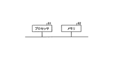
- the figure which shows a processor in case the function of at least one part of the voltage detection means which the power converter device which concerns on Embodiment 1 has, a margin calculation means, a load limitation determination means, and a load control means is implement
- FIG. 1 shows an example of the allowable voltage upper limit value and allowable voltage lower limit value which are memorize
- FIG. 3 The figure which shows the relationship between the primary current and DC voltage when the active converter which the power converter device which concerns on Embodiment 3 has is carrying out the pressure
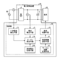
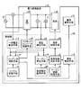
- FIG. 1 is a diagram illustrating a configuration of a power conversion device 1 according to the first embodiment.
- the power conversion apparatus 1 includes a rectifier circuit 2 that rectifies an AC voltage supplied from an AC power supply 20.
- FIG. 1 also shows an AC power supply 20.
- a terminal on the input side of the rectifier circuit 2 is connected to the AC power source 20, and the rectifier circuit 2 rectifies the AC voltage supplied from the AC power source 20 into a DC voltage and outputs it.
- the power converter 1 further has a smoothing capacitor 3 connected to the output side terminal of the rectifier circuit 2.
- An example of the smoothing capacitor 3 is an electrolytic capacitor.
- the smoothing capacitor 3 smoothes a DC voltage that is rectified by the rectifier circuit 2 and includes a ripple voltage.
- the DC voltage whose ripple voltage is reduced by the smoothing capacitor 3 than when the DC voltage from the rectifier circuit 2 is supplied to the smoothing capacitor 3 is supplied from the smoothing capacitor 3 to the load 30 that operates based on the DC voltage.
- the A load 30 is also shown in FIG.
- the power conversion device 1 further includes a control unit 4 that controls the operation of the load 30.
- the control unit 4 stores the voltage detection means 5 that detects the DC voltage rectified by the rectifier circuit 2, and the allowable voltage upper limit value and the allowable voltage lower limit value of the DC voltage used when controlling the operation of the load 30.
- an allowable voltage storage means 6 The allowable voltage upper limit value is an upper limit value of an allowable DC voltage range when the load 30 operates stably.
- the allowable voltage lower limit value is a lower limit value of the allowable DC voltage range. In the first embodiment, both the allowable voltage upper limit value and the allowable voltage lower limit value are constant.
- the control unit 4 includes margin calculation means 7 for calculating an upper limit voltage difference that is a value obtained by subtracting the maximum value of the DC voltage detected by the voltage detection means 5 from the allowable voltage upper limit value stored in the allowable voltage storage means 6. Also have.
- the margin calculation means 7 further calculates a lower limit voltage difference that is a value obtained by subtracting the allowable voltage lower limit value stored in the allowable voltage storage means 6 from the minimum value of the DC voltage detected by the voltage detection means 5.
- the margin calculating means 7 determines the smaller one of the calculated upper limit voltage difference and lower limit voltage difference as the DC voltage margin.
- the control unit 4 further includes margin range storage means 8 for storing a plurality of margin ranges for limiting the operation of the load 30 in a stepwise manner according to the DC voltage margin.
- the control unit 4 determines the restriction on the operation of the load 30 according to the margin range including the DC voltage margin determined by the margin calculation unit 7 among the plurality of margin ranges stored in the margin range storage unit 8.
- Load limiting determination means 9 is further provided.
- the control unit 4 further includes a load control unit 10 that controls the operation of the load 30 in accordance with the limit determined by the load limit determination unit 9.
- Each of the allowable voltage storage means 6 and the margin range storage means 8 includes, for example, RAM (Random Access Memory), ROM (Read Only Memory), flash memory, EPROM (Erasable Programmable Read Only Memory), EEPROM (Electrically Erasable Programmable Read-Ready).
- RAM Random Access Memory
- ROM Read Only Memory
- flash memory EPROM (Erasable Programmable Read Only Memory)
- EEPROM Electrically Erasable Programmable Read-Ready
- Non-volatile or volatile semiconductor memory such as “Only Memory”, magnetic disk, flexible disk, optical disk, compact disk, mini disk, DVD (Digital Versatile Disk), etc.
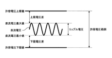
- FIG. 2 is a diagram for explaining the operation of the margin calculating unit 7 when the margin calculating unit 7 included in the power conversion device 1 according to the first embodiment determines a DC voltage margin.
- the margin calculation unit 7 detects the maximum value and the minimum value of the DC voltage detected by the voltage detection unit 5.
- the margin calculation means 7 reads the allowable voltage upper limit value and the allowable voltage lower limit value from the allowable voltage storage means 6.
- the margin calculation means 7 calculates an upper limit voltage difference that is a value obtained by subtracting the maximum value of the DC voltage from the allowable voltage upper limit value, and calculates a lower limit voltage difference that is a value obtained by subtracting the allowable voltage lower limit value from the minimum value of the DC voltage. calculate.
- the margin calculating means 7 determines the smaller one of the calculated upper limit voltage difference and lower limit voltage difference as the DC voltage margin.
- the range above the allowable voltage lower limit and below the allowable voltage upper limit is an allowable voltage range for operating the load 30.
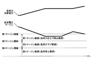
- FIG. 3 shows an example of changes of the power consumption of the load 30 and the DC voltage margin over time when the power conversion device 1 according to Embodiment 1 controls the operation of the load 30, and the power conversion device 1 has It is a figure which shows the 1st margin range memorize
- the symbol t indicates time.
- the first margin range, the second margin range, and the third margin range shown in FIG. 3 are examples of a plurality of margin ranges.
- Each of the plurality of margin ranges is a range set to limit the operation of the load 30 in a stepwise manner according to the DC voltage margin.
- the margin range storage means 8 further stores a first margin threshold, a second margin threshold, and a third margin threshold for specifying the first margin range, the second margin range, and the third margin range.
- the first margin threshold is greater than the second margin threshold
- the second margin threshold is greater than the third margin threshold.
- the first margin threshold is 20V
- the second margin threshold is 10V
- the third margin threshold is 0V.
- the first margin range is a range in which all values included in the first margin range are equal to or smaller than the first margin threshold and larger than the second margin threshold.
- the second margin range is a range in which all values included in the second margin range are equal to or smaller than the second margin threshold and greater than the third margin threshold.
- the third margin range is a range in which all values included in the third margin range are equal to or smaller than the third margin threshold.
- the load limit determining means 9 determines the limit of the operation of the load 30 as follows. That is, the load limit determining unit 9 determines a limit for prohibiting an increase in the operation of the load 30 when the DC voltage margin determined by the margin calculating unit 7 is included in the first margin range. That is, the first margin range is a load increase prohibition range.
- the load limit determining means 9 determines a limit for reducing the operation of the load 30 when the DC voltage margin is included in the second margin range. That is, the second margin range is a load reduction range. More specifically, when the DC voltage margin is included in the second margin range, the load limit determination means 9 is a limit that suppresses the operation of the load 30 more than when the DC voltage margin is included in the first margin range. To decide.
- the load limit determining means 9 determines a limit for stopping the operation of the load 30 when the DC voltage margin is included in the third margin range. That is, the third margin range is a load stop range. More specifically, when the DC voltage margin is included in the third margin range, the load limit determination means 9 is a limit that suppresses the operation of the load 30 more than when the DC voltage margin is included in the second margin range. To decide. When the DC voltage margin is greater than the first margin threshold, the load limit determining unit 9 determines that the load 30 is to be operated normally without limiting the operation. The period in which the DC voltage margin is determined is set by the users of the power conversion device 1 and the load 30. The period at which the limit is determined is also set by the user.
- the load control unit 10 controls the operation of the load 30 in accordance with the limit determined by the load limit determination unit 9. For example, when the load 30 is a motor, the load control unit 10 changes the number of revolutions per unit time of the motor according to the limit determined by the load limit determination unit 9. For example, when the load 30 is a variable resistance, the load control unit 10 changes the value of the resistance according to the limit determined by the load limit determination unit 9.
- the load control unit 10 determines the number of revolutions per unit time of the motor when the DC voltage margin determined by the margin calculation unit 7 is included in the first margin range. Control that does not increase When the DC voltage margin is included in the second margin range, the load control means 10 reduces the rotational speed per unit time of the motor. The load control means 10 stops the rotation of the motor when the DC voltage margin is included in the third margin range.
- the operation of the compressor motor may be affected by the configuration of the refrigerant circuit.
- the power conversion device 1 reduces the number of rotations per unit time of the compressor motor. This suppresses the burden on the compressor motor.
- the power converter 1 rotates the number of rotations per unit time of the compressor motor. Decrease. Even if the number of rotations per unit time decreases, the reduction of the burden on the compressor may be delayed. That is, there is a concern that the DC voltage margin undershoots.
- it is preferable that one or both of the interval between the first margin threshold and the second margin threshold and the interval between the second margin threshold and the third margin threshold are set to be relatively large.
- the margin calculating unit 7 determines the maximum value of the DC voltage detected by the voltage detecting unit 5 from the allowable voltage upper limit value stored in the allowable voltage storage unit 6. And a lower limit voltage that is a value obtained by subtracting the allowable voltage lower limit value stored in the allowable voltage storage means 6 from the minimum value of the DC voltage detected by the voltage detection means 5. Calculate the difference.
- the difference between the maximum value and the minimum value of the DC voltage detected by the voltage detection means 5 is a ripple voltage.
- the margin calculating means 7 determines the smaller one of the calculated upper limit voltage difference and lower limit voltage difference as the DC voltage margin.
- the load limit determining means 9 limits the operation of the load 30 according to the margin range including the DC voltage margin determined by the margin calculating means 7 out of the plurality of margin ranges stored in the margin range storage means 8. decide.
- the load control unit 10 controls the operation of the load 30 according to the limit determined by the load limit determination unit 9.
- the operation of the load 30 that operates based on the DC voltage including the ripple voltage can be controlled according to the magnitude of the ripple voltage. Furthermore, in the power converter 1, the operation of the load 30 can be controlled stepwise according to the magnitude of the ripple voltage.
- the power conversion apparatus 1 controls the operation of the load 30 according to the magnitude of the ripple voltage, the ripple removal capability of the smoothing capacitor 3 is maximized in real time, and the rectified DC voltage is applied to the load 30. Can be held in a voltage range for stable operation.
- the operation of the load 30 is started in a relatively low temperature environment, there is a possibility that the operation of the load 30 is limited in a state where the ripple removal capability of the smoothing capacitor 3 is low.
- the power converter 1 can release the restriction on the load 30. That is, the power conversion device 1 can stably operate the load 30 even when the load 30 starts to operate in a relatively low temperature environment.
- the power converter 1 controls the operation of the load 30 in a stepwise manner according to the magnitude of the ripple voltage, even if the ripple removal capability of the smoothing capacitor 3 is lower than the capability assumed in advance, the load 30 The operation can be appropriately controlled.
- the load 30 is a compressor motor of an air conditioner
- the air temperature in the space where the indoor unit of the air conditioner is provided approaches the set temperature when the operation of the compressor motor is restricted. Takes a long time.
- the power conversion device 1 can avoid a situation in which the compressor motor does not operate completely.
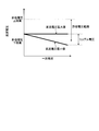
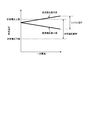
- FIG. 4 is a diagram illustrating that the minimum value of the DC voltage detected by the voltage detection unit 5 included in the power conversion device 1 according to Embodiment 1 decreases in proportion to the magnitude of the primary current. Even when the minimum value of the DC voltage decreases in proportion to the magnitude of the primary current, the margin calculating means 7 stores the minimum value of the DC voltage detected by the voltage detecting means 5 in the allowable voltage storage means 6. The lower limit voltage difference which is a value obtained by subtracting the allowable voltage lower limit value is calculated.
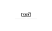
- FIG. 5 shows that at least a part of components constituting the voltage detection means 5, margin calculation means 7, load limit determination means 9, and load control means 10 included in the power conversion device 1 according to the first embodiment are processed by the processing circuit 51. It is a figure which shows the processing circuit 51 in the case of implement
- the processing circuit 51 is dedicated hardware.
- the processing circuit 51 is, for example, a single circuit, a composite circuit, a programmed processor, a parallel programmed processor, an ASIC (Application Specific Integrated Circuit), an FPGA (Field-Programmable Gate Array), or a combination thereof. It is.
- a part of the voltage detection means 5, the margin calculation means 7, the load limit determination means 9, and the load control means 10 may be dedicated hardware that is separate from the rest.
- FIG. 6 shows a case where at least some of the functions of the voltage detection means 5, margin calculation means 7, load limit determination means 9, and load control means 10 included in the power conversion device 1 according to the first embodiment are realized by the processor 61.
- the processor 61 is a CPU (Central Processing Unit), a processing device, an arithmetic device, a microprocessor, a microcomputer, or a DSP (Digital Signal Processor).
- FIG. 6 also shows the memory 62.
- the partial function includes the processor 61, software, firmware, Alternatively, it is realized by a combination of software and firmware.
- Software or firmware is described as a program and stored in the memory 62.
- the processor 61 reads out and executes a program stored in the memory 62, thereby realizing at least some functions of the voltage detection unit 5, the margin calculation unit 7, the load limit determination unit 9, and the load control unit 10.
- the power conversion apparatus 1 includes the voltage detection unit 5, the margin calculation The memory 62 for storing the program in which the steps executed by the means 7, the load limit determining means 9 and the part of the load control means 10 are executed as a result. It can be said that the program stored in the memory 62 causes the computer to execute a procedure or method executed by a part of the voltage detection means 5, the margin calculation means 7, the load limit determination means 9, and the load control means 10.
- the memory 62 is, for example, a nonvolatile or volatile semiconductor memory such as RAM, ROM, flash memory, EPROM, or EEPROM, a magnetic disk, a flexible disk, an optical disk, a compact disk, a mini disk, or a DVD.
- a nonvolatile or volatile semiconductor memory such as RAM, ROM, flash memory, EPROM, or EEPROM, a magnetic disk, a flexible disk, an optical disk, a compact disk, a mini disk, or a DVD.
- the plurality of functions of the voltage detection unit 5, the margin calculation unit 7, the load limit determination unit 9, and the load control unit 10 a part of the plurality of functions is realized by dedicated hardware, and the rest of the plurality of functions is software. Alternatively, it may be realized by firmware. As described above, the plurality of functions of the voltage detection unit 5, the margin calculation unit 7, the load limit determination unit 9, and the load control unit 10 can be realized by hardware, software, firmware, or a combination thereof.
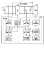
- FIG. FIG. 7 is a diagram illustrating a configuration of a power conversion device 1A according to the second embodiment.
- 1 A of power converters have the rectifier circuit 2, the smoothing capacitor 3, the voltage detection means 5, the margin range memory
- the control unit 4 of the first embodiment is replaced with a control unit 4A.
- differences from the first embodiment will be mainly described.
- the primary current detection means 11 which detects the primary current which flows into the rectifier circuit 2 from the alternating current power supply 20.
- FIG. The primary current detection means 11 is connected to the input side terminal of the rectifier circuit 2.
- the primary current detection unit 11 is included in a control unit 4A having a voltage detection unit 5, a margin range storage unit 8, a load limit determination unit 9, and a load control unit 10.
- the allowable voltage storage means 6 of the first embodiment is replaced with an allowable voltage storage means 6A.
- the allowable voltage storage unit 6A is included in the control unit 4A.
- the allowable voltage storage means 6A stores an allowable voltage upper limit value and an allowable voltage lower limit value for each of a plurality of primary currents. That is, the allowable voltage storage means 6A stores a plurality of sets of allowable voltage upper limit values and allowable voltage lower limit values, and the plurality of sets correspond to a plurality of primary currents.
- the allowable voltage storage means 6A is, for example, a nonvolatile or volatile semiconductor memory such as RAM, ROM, flash memory, EPROM, or EEPROM, a magnetic disk, a flexible disk, an optical disk, a compact disk, a mini disk, or a DVD.
- FIG. 8 is a diagram illustrating an example of the allowable voltage upper limit value and the allowable voltage lower limit value stored in the allowable voltage storage unit 6A of the power conversion device 1A according to the second embodiment.
- both the allowable voltage upper limit value and the allowable voltage lower limit value are constant.
- the allowable voltage upper limit value is constant regardless of the primary current, but the allowable voltage lower limit value increases as the primary current increases.
- the allowable voltage lower limit value is directly proportional to the magnitude of the primary current.
- the margin calculating means 7 in the first embodiment is replaced with a margin calculating means 7A.
- the margin calculating means 7A is included in the control unit 4A.
- the margin calculating means 7A is a set of permissible voltages corresponding to the primary current detected by the primary current detecting means 11 out of a plurality of permissible voltage upper limit values and permissible voltage lower limit values stored in the permissible voltage storage means 6A.
- the upper limit voltage difference and the lower limit voltage difference are calculated using the upper limit value and the allowable voltage lower limit value in the same manner as the margin calculating means 7.
- the margin calculating means 7A determines the smaller one of the calculated upper limit voltage difference and lower limit voltage difference as the DC voltage margin.
- the power conversion device 1A uses the set of allowable voltage upper limit value and allowable voltage lower limit value corresponding to the primary current detected by the primary current detection unit 11, and uses the upper limit voltage difference and the lower limit voltage. Calculate the difference. That is, the power conversion device 1A can control the operation of the load 30 according to the magnitude of the ripple voltage in consideration of the primary current.
- the minimum value of the DC voltage corresponding to the capacity of the smoothing capacitor 3 is indicated by a broken line.
- an example of the minimum value of the DC voltage when the capacitance of the smoothing capacitor 3 is relatively large is indicated by a first broken line L1
- the capacitance of the smoothing capacitor 3 is relatively intermediate.
- An example of the minimum value of the DC voltage in a certain case is indicated by the second broken line L2
- an example of the minimum value of the DC voltage when the capacitance of the smoothing capacitor 3 is relatively small is indicated by the third broken line L3. .
- a character string “smoothing capacitor (large)” is added to the first broken line L1
- a character string “smoothing capacitor (medium)” is added to the second broken line L2.
- a character string “smoothing capacitor (small)” is added to the broken line L3.
- the cross point between the solid line and the broken line is a point at which the DC voltage margin determined by the margin calculating means 7A becomes 0V.
- the DC voltage of the smoothing capacitor 3 decreases as the primary current increases regardless of the capacity.
- the allowable voltage upper limit value is constant, but the allowable voltage upper limit value may not be constant.
- the allowable voltage storage means 6A stores the allowable voltage upper limit value and the allowable voltage lower limit value for each of the plurality of primary currents.
- At least some of the functions constituting the voltage detection means 5, the margin calculation means 7A, the load limit determination means 9, the load control means 10 and the primary current detection means 11 included in the power conversion device 1A according to the second embodiment are as follows. It may be realized by a processing circuit having the same function as the processing circuit 51 described in the first embodiment.
- the power conversion device 1A includes the voltage detection means 5 And a memory for storing a program in which the steps executed by at least a part of the margin calculating means 7A, the load limit determining means 9, the load control means 10 and the primary current detecting means 11 are executed as a result.
- the memory is a memory having the same function as the memory 62 described in the first embodiment.
- FIG. 9 is a diagram illustrating a configuration of the power conversion device 1B according to the third embodiment.
- the power conversion device 1B includes a smoothing capacitor 3, a voltage detection unit 5, an allowable voltage storage unit 6A, a margin calculation unit 7A, a margin range storage unit 8, a load limit determination unit 9, and the power conversion device 1A according to the second embodiment.
- Load control means 10 and primary current detection means 11 are provided.
- the power conversion device 1B includes an active converter 2B having a function of boosting an AC voltage to an arbitrary DC voltage, instead of the rectifier circuit 2 of the second embodiment.
- the control unit 4A of the second embodiment is replaced with a control unit 4B.
- differences from the second embodiment will be mainly described.
- the power conversion device 1B includes a ripple storage unit 12 that stores a ripple voltage range when the smoothing capacitor 3 is specified in advance as normal for each of a plurality of primary currents.
- the ripple storage unit 12 is connected to the control unit 4B having the voltage detection unit 5, the allowable voltage storage unit 6A, the margin calculation unit 7A, the margin range storage unit 8, the load limit determination unit 9, the load control unit 10, and the primary current detection unit 11. Is included.
- the ripple storage means 12 is, for example, a nonvolatile or volatile semiconductor memory such as RAM, ROM, flash memory, EPROM, or EEPROM, a magnetic disk, a flexible disk, an optical disk, a compact disk, a mini disk, or a DVD.
- the power conversion device 1B further includes capacitor determining means 13 for determining whether or not the smoothing capacitor 3 is normal.
- the capacitor determination unit 13 is included in the control unit 4B.
- the capacitor determination unit 13 calculates a ripple voltage from the DC voltage detected by the voltage detection unit 5. Specifically, the capacitor determination unit 13 calculates the ripple voltage by subtracting the minimum value from the maximum value of the DC voltage detected by the voltage detection unit 5.
- the capacitor determination unit 13 compares the ripple voltage range corresponding to the primary current detected by the primary current detection unit 11 among the plurality of ripple voltage ranges stored in the ripple storage unit 12 with the calculated ripple voltage. Then, it is determined whether or not the smoothing capacitor 3 is normal. Specifically, the capacitor determination unit 13 determines the ripple voltage corresponding to the primary current detected by the primary current detection unit 11 among the plurality of ripple voltage ranges in which the calculated ripple voltage is stored in the ripple storage unit 12. When it is determined whether or not the calculated ripple voltage is included in the range, the smoothing capacitor 3 is determined to be normal when it is determined that the calculated ripple voltage is included in the corresponding ripple voltage range.
- the power conversion device 1B further includes active converter control means 14 for controlling the active converter 2B.
- the active converter control means 14 is included in the control unit 4B.
- the active converter control unit 14 causes the active converter 2B to perform a boosting operation only when the capacitor determination unit 13 determines that the smoothing capacitor 3 is normal.
- the active converter 2B performs a boosting operation. That is, the power conversion device 1B can increase the voltage supplied to the load 30 only when the smoothing capacitor 3 is normal.
- FIG. 10 is a diagram illustrating a relationship between the primary current and the DC voltage when the active converter 2B included in the power conversion device 1B according to the third embodiment is performing a boosting operation.
- the maximum value of the DC voltage detected by the voltage detector 5 increases as the value of the primary current detected by the primary current detector 11 increases.
- the difference between the minimum value and the minimum value increases. That is, when the active converter 2B is performing a boosting operation, the ripple voltage increases as the primary current value increases. For example, when the active converter 2B performs a boost operation, the ripple voltage is directly proportional to the magnitude of the primary current.
- the magnitude of the ripple voltage included in the DC voltage rectified by the active converter 2B is large in the capacitance of the smoothing capacitor 3. Small enough.
- the ripple voltage increases as the magnitude of the primary current increases.
- the capacitor determination means 13 It is possible to appropriately determine whether 3 is normal.
- the active converter control means 14 When the active converter 2B starts the boosting operation, the active converter control means 14 does not have a possibility that the maximum value of the DC voltage including the ripple voltage after the boosting exceeds the upper limit value of the DC voltage allowed for the load 30. Whether or not the smoothing capacitor 3 is normal is further included. Therefore, the active converter control means 14 causes the allowable voltage upper limit value to exceed the maximum value of the DC voltage including the ripple voltage when the active converter 2B starts the boosting operation in a state where the capacitance of the smoothing capacitor 3 is low. Can be avoided.
- Capacitor determining means 13 determines whether or not smoothing capacitor 3 has a capacity characteristic that can suppress the overshoot of the DC voltage, which is a concern immediately after active converter 2B starts the boosting operation. It has the function to judge based on.
- the active converter control means 14 has no possibility that the maximum value of the DC voltage including the ripple voltage after boosting when the active converter 2B starts the boosting operation exceeds the upper limit value of the DC voltage allowed for the load 30. Always determine whether or not. Accordingly, when the temperature around the smoothing capacitor 3 rises after the load 30 starts in a relatively low temperature environment and the smoothing capacitor 3 recovers to a normal state, the active converter control means 14 When the normal state is restored, the active converter 2B can be boosted.
- the case where the smoothing capacitor 3 is restored to a normal state is a case where the smoothing capacitor 3 is restored to a state where overshoot of the DC voltage can be suppressed.
- the power converter 1B is executed by at least a part of the voltage detection means 5, the margin calculation means 7A, the load limit determination means 9, the load control means 10, the primary current detection means 11, the capacitor determination means 13, and the active converter control means 14.
- the memory is a memory having the same function as the memory 62 described in the first embodiment.
- FIG. 11 is a diagram showing a configuration of a power conversion device 1C according to the fourth embodiment.
- the power conversion device 1C includes an active converter 2B, a smoothing capacitor 3, a voltage detection unit 5, an allowable voltage storage unit 6A, a margin calculation unit 7A, a margin range storage unit 8, and a load limiter included in the power conversion device 1B according to the third embodiment. It has a determination means 9, a load control means 10, a primary current detection means 11, a ripple storage means 12, a capacitor determination means 13, and an active converter control means 14.
- the control unit 4B of the third embodiment is replaced with a control unit 4C.
- differences from the third embodiment will be mainly described.
- the power conversion device 1C further includes an abnormality detection unit 15 that determines that an abnormality has occurred when the smoothing capacitor 3 is not normally determined to be normal for a predetermined period by the capacitor determination unit 13.
- the abnormality detection unit 15 determines that an abnormality has occurred even when the load limit determination unit 9 determines to continuously limit the operation of the load 30 for a predetermined period.
- the abnormality detection means 15 includes a voltage detection means 5, an allowable voltage storage means 6A, a margin calculation means 7A, a margin range storage means 8, a load limit determination means 9, a load control means 10, a primary current detection means 11, a ripple storage means 12, It is included in the control unit 4C having the capacitor determination means 13 and the active converter control means 14.
- the power conversion device 1C further includes an abnormality notifying unit 16 for notifying that an abnormality has occurred outside the power conversion device 1C when the abnormality detection unit 15 determines that an abnormality has occurred.
- An example of the abnormality notifying means 16 is a display device that displays that an abnormality has occurred.
- Another example of the abnormality notifying means 16 is a speaker that notifies by sound that an abnormality has occurred.
- the power converter 1C determines that an abnormality has occurred when the smoothing capacitor 3 is not normal continuously for a predetermined period or when the operation of the load 30 is restricted, and an abnormality has occurred outside the power converter 1C. Notify that The user can deal with the abnormality by notifying that the abnormality has occurred. For example, the user can take measures to replace the active converter 2B or the smoothing capacitor 3 with a normal one. That is, the power conversion device 1 ⁇ / b> C can cause the user to deal with the abnormality early when an abnormality occurs. Furthermore, the power conversion device 1C can shorten the period during which the load 30 cannot operate.
- the power conversion device 1C determines that an abnormality has occurred when the smoothing capacitor 3 is not normal continuously for a predetermined period or when the operation of the load 30 is limited. Since a predetermined period is set, the power conversion device 1C can determine that an unstable state immediately after the operation of the load 30 in a relatively low temperature environment is not abnormal, for example.
- the abnormality detection unit 15 may determine the content of the abnormality according to the degree of restriction or the restricted period when the operation of the load 30 is restricted. In that case, the abnormality notifying unit 16 also notifies the abnormality of the content determined by the abnormality detecting unit 15 to the outside of the power converter 1C. The user can take more appropriate measures against the abnormality by notifying the content of the abnormality.
- the smoothing capacitor 3 may be a capacitor that has a function that is less likely to deteriorate over time than a function that suppresses ripple voltage.
- At least some of the functions constituting the abnormality detection unit 15 and the abnormality notification unit 16 may be realized by a processing circuit having the same function as the processing circuit 51 described in the first embodiment.
- At least one of voltage detection means 5, margin calculation means 7A, load limit determination means 9, load control means 10, primary current detection means 11, capacitor determination means 13, active converter control means 14, abnormality detection means 15 and abnormality notification means 16 The function of the unit may be realized by a processor having the same function as the processor 61 described in the first embodiment.
- the power conversion device 1C includes a voltage detection unit 5, a margin calculation unit 7A, a load limit determination unit 9, a load control unit 10, a primary current detection unit 11, a capacitor determination unit 13, an active It has a memory for storing a program in which the steps executed by at least a part of the converter control means 14, the abnormality detection means 15 and the abnormality notification means 16 are executed as a result.
- the memory is a memory having the same function as the memory 62 described in the first embodiment.
- the configuration described in the above embodiment shows an example of the contents of the present invention, and can be combined with another known technique, and can be combined with other configurations without departing from the gist of the present invention. It is also possible to omit or change the part.
Landscapes
- Engineering & Computer Science (AREA)
- Power Engineering (AREA)
- Dc-Dc Converters (AREA)
- Rectifiers (AREA)
- Power Conversion In General (AREA)
Abstract
Description
図1は、実施の形態1に係る電力変換装置1の構成を示す図である。電力変換装置1は、交流電源20から供給される交流電圧を整流する整流回路2を有する。図1には、交流電源20も示されている。整流回路2の入力側の端子が交流電源20に接続されており、整流回路2は交流電源20から供給される交流電圧を直流電圧に整流して出力する。
図7は、実施の形態2に係る電力変換装置1Aの構成を示す図である。電力変換装置1Aは、実施の形態1に係る電力変換装置1が有する整流回路2、平滑コンデンサ3、電圧検出手段5、マージン範囲記憶手段8、負荷制限決定手段9及び負荷制御手段10を有する。実施の形態2では、実施の形態1の制御部4は制御部4Aに置き換えられている。実施の形態2では、実施の形態1との相違点を主に説明する。
図9は、実施の形態3に係る電力変換装置1Bの構成を示す図である。電力変換装置1Bは、実施の形態2に係る電力変換装置1Aが有する平滑コンデンサ3、電圧検出手段5、許容電圧記憶手段6A、マージン算出手段7A、マージン範囲記憶手段8、負荷制限決定手段9、負荷制御手段10及び一次電流検出手段11を有する。電力変換装置1Bは、実施の形態2の整流回路2に代えて、交流電圧を任意の直流電圧に昇圧する機能を有するアクティブコンバータ2Bを有する。実施の形態3では、実施の形態2の制御部4Aは制御部4Bに置き換えられている。実施の形態3では、実施の形態2との相違点を主に説明する。
図11は、実施の形態4に係る電力変換装置1Cの構成を示す図である。電力変換装置1Cは、実施の形態3に係る電力変換装置1Bが有するアクティブコンバータ2B、平滑コンデンサ3、電圧検出手段5、許容電圧記憶手段6A、マージン算出手段7A、マージン範囲記憶手段8、負荷制限決定手段9、負荷制御手段10、一次電流検出手段11、リップル記憶手段12、コンデンサ判断手段13及びアクティブコンバータ制御手段14を有する。実施の形態4では、実施の形態3の制御部4Bは制御部4Cに置き換えられている。実施の形態4では、実施の形態3との相違点を主に説明する。
Claims (5)
- 交流電源から供給される交流電圧を整流する整流回路と、
前記整流回路によって整流された直流電圧であってリップル電圧を含む直流電圧を平滑する平滑コンデンサと、
前記整流回路によって整流された直流電圧を検出する電圧検出手段と、
前記平滑コンデンサによって平滑された直流電圧をもとに動作する負荷の動作を制御する際に用いられる直流電圧の許容電圧上限値と許容電圧下限値とを記憶する許容電圧記憶手段と、
前記許容電圧記憶手段に記憶されている前記許容電圧上限値から前記電圧検出手段によって検出された直流電圧の最大値を減じた値である上限電圧差と、前記電圧検出手段によって検出された直流電圧の最小値から前記許容電圧記憶手段に記憶されている前記許容電圧下限値を減じた値である下限電圧差とを算出し、前記上限電圧差と前記下限電圧差とのうちの値が小さい方を直流電圧マージンに決定するマージン算出手段と、
前記負荷の動作を段階的に制限するための複数のマージン範囲を記憶するマージン範囲記憶手段と、
前記マージン範囲記憶手段に記憶されている前記複数のマージン範囲のうちの前記マージン算出手段によって決定された直流電圧マージンが含まれるマージン範囲に応じて前記負荷の動作の制限を決定する負荷制限決定手段と、
前記負荷制限決定手段によって決定された制限に応じて前記負荷の動作を制御する負荷制御手段と
を備えることを特徴とする電力変換装置。 - 前記交流電源から前記整流回路に流れる一次電流を検出する一次電流検出手段を更に備え、
前記許容電圧記憶手段は、複数の一次電流の各々について前記許容電圧上限値及び前記許容電圧下限値を記憶しており、
前記マージン算出手段は、前記許容電圧記憶手段に記憶されている複数の前記許容電圧上限値及び前記許容電圧下限値の組のうちの前記一次電流検出手段によって検出された一次電流に対応する組の前記許容電圧上限値及び前記許容電圧下限値を用いて、前記上限電圧差及び前記下限電圧差を算出する
ことを特徴とする請求項1に記載の電力変換装置。 - 複数の前記一次電流の各々について前記平滑コンデンサが正常であるとあらかじめ特定されている場合のリップル電圧範囲を記憶するリップル記憶手段と、
前記電圧検出手段によって検出された直流電圧からリップル電圧を算出し、前記リップル記憶手段に記憶されている複数の前記リップル電圧範囲のうちの前記一次電流検出手段によって検出された一次電流に対応するリップル電圧範囲と算出されたリップル電圧とを対比して前記平滑コンデンサが正常であるか否かを判断するコンデンサ判断手段と、
前記整流回路を制御するアクティブコンバータ制御手段とを更に備え、
前記整流回路は、前記交流電圧を任意の直流電圧に昇圧する機能を有するアクティブコンバータであって、
前記アクディブコンバータ制御手段は、前記平滑コンデンサが正常であると前記コンデンサ判断手段によって判断された場合にのみ、前記アクティブコンバータに昇圧動作を行わせる
ことを特徴とする請求項2に記載の電力変換装置。 - あらかじめ定められた期間で連続して前記平滑コンデンサが正常であると前記コンデンサ判断手段によって判断されない場合に異常が発生したと判断する異常検出手段と、
異常が発生したと前記異常検出手段によって判断された場合に前記電力変換装置の外部に異常が発生したことを報知する異常報知手段と
を更に備えることを特徴とする請求項3に記載の電力変換装置。 - 前記異常検出手段は、前記負荷制限決定手段があらかじめ定められた期間で連続して前記負荷の動作を制限することを決定した場合にも異常が発生したと判断する
ことを特徴とする請求項4に記載の電力変換装置。
Priority Applications (3)
| Application Number | Priority Date | Filing Date | Title |
|---|---|---|---|
| EP17911341.0A EP3633835B1 (en) | 2017-05-24 | 2017-05-24 | Power conversion device |
| PCT/JP2017/019386 WO2018216144A1 (ja) | 2017-05-24 | 2017-05-24 | 電力変換装置 |
| JP2019519883A JP6758493B2 (ja) | 2017-05-24 | 2017-05-24 | 電力変換装置 |
Applications Claiming Priority (1)
| Application Number | Priority Date | Filing Date | Title |
|---|---|---|---|
| PCT/JP2017/019386 WO2018216144A1 (ja) | 2017-05-24 | 2017-05-24 | 電力変換装置 |
Publications (1)
| Publication Number | Publication Date |
|---|---|
| WO2018216144A1 true WO2018216144A1 (ja) | 2018-11-29 |
Family
ID=64396309
Family Applications (1)
| Application Number | Title | Priority Date | Filing Date |
|---|---|---|---|
| PCT/JP2017/019386 Ceased WO2018216144A1 (ja) | 2017-05-24 | 2017-05-24 | 電力変換装置 |
Country Status (3)
| Country | Link |
|---|---|
| EP (1) | EP3633835B1 (ja) |
| JP (1) | JP6758493B2 (ja) |
| WO (1) | WO2018216144A1 (ja) |
Cited By (1)
| Publication number | Priority date | Publication date | Assignee | Title |
|---|---|---|---|---|
| WO2022065241A1 (ja) * | 2020-09-28 | 2022-03-31 | 富士電機株式会社 | 電力変換装置 |
Citations (6)
| Publication number | Priority date | Publication date | Assignee | Title |
|---|---|---|---|---|
| JPS5925425B2 (ja) | 1973-12-22 | 1984-06-18 | 株式会社東芝 | テレビジヨン受像機の雑音除去装置 |
| JP2007159176A (ja) * | 2005-11-30 | 2007-06-21 | Hitachi Ltd | 電源装置 |
| JP2012023891A (ja) | 2010-07-15 | 2012-02-02 | Mitsubishi Electric Corp | 電源装置及び照明器具 |
| JP2012095511A (ja) * | 2010-10-29 | 2012-05-17 | Mitsubishi Electric Corp | 電力変換装置 |
| JP2013059257A (ja) * | 2012-12-10 | 2013-03-28 | Mitsubishi Electric Corp | 電力変換装置 |
| JP2013135516A (ja) * | 2011-12-26 | 2013-07-08 | Mitsubishi Heavy Ind Ltd | 電力変換装置及び空気調和機 |
Family Cites Families (3)
| Publication number | Priority date | Publication date | Assignee | Title |
|---|---|---|---|---|
| JP4765689B2 (ja) * | 2006-03-10 | 2011-09-07 | 株式会社富士通ゼネラル | 平滑コンデンサの劣化検出回路及びこれを備えた電子機器 |
| WO2015140867A1 (ja) * | 2014-03-15 | 2015-09-24 | 三菱電機株式会社 | モータ駆動制御装置、圧縮機、送風機、及び空気調和機 |
| JP5931148B2 (ja) * | 2014-09-10 | 2016-06-08 | ファナック株式会社 | 静電容量計算部を有するpwm整流器 |
-
2017
- 2017-05-24 WO PCT/JP2017/019386 patent/WO2018216144A1/ja not_active Ceased
- 2017-05-24 EP EP17911341.0A patent/EP3633835B1/en active Active
- 2017-05-24 JP JP2019519883A patent/JP6758493B2/ja not_active Expired - Fee Related
Patent Citations (6)
| Publication number | Priority date | Publication date | Assignee | Title |
|---|---|---|---|---|
| JPS5925425B2 (ja) | 1973-12-22 | 1984-06-18 | 株式会社東芝 | テレビジヨン受像機の雑音除去装置 |
| JP2007159176A (ja) * | 2005-11-30 | 2007-06-21 | Hitachi Ltd | 電源装置 |
| JP2012023891A (ja) | 2010-07-15 | 2012-02-02 | Mitsubishi Electric Corp | 電源装置及び照明器具 |
| JP2012095511A (ja) * | 2010-10-29 | 2012-05-17 | Mitsubishi Electric Corp | 電力変換装置 |
| JP2013135516A (ja) * | 2011-12-26 | 2013-07-08 | Mitsubishi Heavy Ind Ltd | 電力変換装置及び空気調和機 |
| JP2013059257A (ja) * | 2012-12-10 | 2013-03-28 | Mitsubishi Electric Corp | 電力変換装置 |
Cited By (2)
| Publication number | Priority date | Publication date | Assignee | Title |
|---|---|---|---|---|
| WO2022065241A1 (ja) * | 2020-09-28 | 2022-03-31 | 富士電機株式会社 | 電力変換装置 |
| JP2022054992A (ja) * | 2020-09-28 | 2022-04-07 | 富士電機株式会社 | 電力変換装置 |
Also Published As
| Publication number | Publication date |
|---|---|
| EP3633835A4 (en) | 2020-06-10 |
| JP6758493B2 (ja) | 2020-09-23 |
| EP3633835A1 (en) | 2020-04-08 |
| EP3633835B1 (en) | 2021-03-31 |
| JPWO2018216144A1 (ja) | 2019-08-08 |
Similar Documents
| Publication | Publication Date | Title |
|---|---|---|
| JP5279796B2 (ja) | 電力変換装置 | |
| JP3740946B2 (ja) | 電源装置と、電動機駆動装置および空気調和機 | |
| JP6505256B2 (ja) | 空気調和機 | |
| JP3655077B2 (ja) | 電源装置 | |
| JP5381229B2 (ja) | コンデンサの劣化検出回路及びこれを備えた電子機器 | |
| JP5460838B2 (ja) | 電力変換装置 | |
| US10447194B2 (en) | Motor drive apparatus, blower, motor driving method, and storage medium | |
| JP6758493B2 (ja) | 電力変換装置 | |
| JP2017123740A (ja) | スイッチング電源 | |
| JP2013212000A (ja) | 電動コンプレッサ | |
| WO2021240597A1 (ja) | 直流電源装置およびその制御方法 | |
| JP6319120B2 (ja) | 空気調和機 | |
| WO2016103325A1 (ja) | 電力変換装置 | |
| JP2020150610A (ja) | 電源装置及びこれを備えた空気調和機 | |
| US11973452B2 (en) | Fan motor stopping apparatus | |
| JP2022027254A (ja) | 補助電源装置及びプログラム | |
| JP2005318700A (ja) | 電源装置 | |
| JP6641501B2 (ja) | コンバータ制御装置およびコンバータ制御方法 | |
| JP4561493B2 (ja) | 空気調和機 | |
| JP6958387B2 (ja) | 直流電源装置および直流電源装置の制御方法 | |
| JP7049770B2 (ja) | 電力変換装置ならびモータ駆動システム | |
| JP2003222417A (ja) | 空気調和機 | |
| JP6045308B2 (ja) | アクティブコンバータの制御装置およびその方法ならびにプログラム | |
| WO2022230062A1 (ja) | 電力変換装置および電力変換装置における突入電流抑制方法 | |
| JPWO2020194755A1 (ja) | モータ駆動装置 |
Legal Events
| Date | Code | Title | Description |
|---|---|---|---|
| 121 | Ep: the epo has been informed by wipo that ep was designated in this application |
Ref document number: 17911341 Country of ref document: EP Kind code of ref document: A1 |
|
| ENP | Entry into the national phase |
Ref document number: 2019519883 Country of ref document: JP Kind code of ref document: A |
|
| NENP | Non-entry into the national phase |
Ref country code: DE |
|
| WWE | Wipo information: entry into national phase |
Ref document number: 2017911341 Country of ref document: EP |
|
| ENP | Entry into the national phase |
Ref document number: 2017911341 Country of ref document: EP Effective date: 20200102 |