WO2018220910A1 - Corps fritté de nitrure de bore cubique revêtu en surface et outil de coupe doté de ce dernier - Google Patents
Corps fritté de nitrure de bore cubique revêtu en surface et outil de coupe doté de ce dernier Download PDFInfo
- Publication number
- WO2018220910A1 WO2018220910A1 PCT/JP2018/006170 JP2018006170W WO2018220910A1 WO 2018220910 A1 WO2018220910 A1 WO 2018220910A1 JP 2018006170 W JP2018006170 W JP 2018006170W WO 2018220910 A1 WO2018220910 A1 WO 2018220910A1
- Authority
- WO
- WIPO (PCT)
- Prior art keywords
- coating
- boron nitride
- cubic boron
- interface
- less
- Prior art date
- Legal status (The legal status is an assumption and is not a legal conclusion. Google has not performed a legal analysis and makes no representation as to the accuracy of the status listed.)
- Ceased
Links
Images

Classifications
-
- B—PERFORMING OPERATIONS; TRANSPORTING
- B23—MACHINE TOOLS; METAL-WORKING NOT OTHERWISE PROVIDED FOR
- B23B—TURNING; BORING
- B23B27/00—Tools for turning or boring machines; Tools of a similar kind in general; Accessories therefor
- B23B27/14—Cutting tools of which the bits or tips or cutting inserts are of special material
-
- B—PERFORMING OPERATIONS; TRANSPORTING
- B23—MACHINE TOOLS; METAL-WORKING NOT OTHERWISE PROVIDED FOR
- B23B—TURNING; BORING
- B23B27/00—Tools for turning or boring machines; Tools of a similar kind in general; Accessories therefor
- B23B27/14—Cutting tools of which the bits or tips or cutting inserts are of special material
- B23B27/18—Cutting tools of which the bits or tips or cutting inserts are of special material with cutting bits or tips or cutting inserts rigidly mounted, e.g. by brazing
- B23B27/20—Cutting tools of which the bits or tips or cutting inserts are of special material with cutting bits or tips or cutting inserts rigidly mounted, e.g. by brazing with diamond bits or cutting inserts
-
- B—PERFORMING OPERATIONS; TRANSPORTING
- B23—MACHINE TOOLS; METAL-WORKING NOT OTHERWISE PROVIDED FOR
- B23B—TURNING; BORING
- B23B51/00—Tools for drilling machines
-
- B—PERFORMING OPERATIONS; TRANSPORTING
- B23—MACHINE TOOLS; METAL-WORKING NOT OTHERWISE PROVIDED FOR
- B23C—MILLING
- B23C5/00—Milling-cutters
- B23C5/16—Milling-cutters characterised by physical features other than shape
-
- B—PERFORMING OPERATIONS; TRANSPORTING
- B23—MACHINE TOOLS; METAL-WORKING NOT OTHERWISE PROVIDED FOR
- B23D—PLANING; SLOTTING; SHEARING; BROACHING; SAWING; FILING; SCRAPING; LIKE OPERATIONS FOR WORKING METAL BY REMOVING MATERIAL, NOT OTHERWISE PROVIDED FOR
- B23D77/00—Reaming tools
-
- B—PERFORMING OPERATIONS; TRANSPORTING
- B23—MACHINE TOOLS; METAL-WORKING NOT OTHERWISE PROVIDED FOR
- B23F—MAKING GEARS OR TOOTHED RACKS
- B23F21/00—Tools specially adapted for use in machines for manufacturing gear teeth
-
- B—PERFORMING OPERATIONS; TRANSPORTING
- B23—MACHINE TOOLS; METAL-WORKING NOT OTHERWISE PROVIDED FOR
- B23G—THREAD CUTTING; WORKING OF SCREWS, BOLT HEADS, OR NUTS, IN CONJUNCTION THEREWITH
- B23G5/00—Thread-cutting tools; Die-heads
- B23G5/02—Thread-cutting tools; Die-heads without means for adjustment
- B23G5/06—Taps
-
- C—CHEMISTRY; METALLURGY
- C04—CEMENTS; CONCRETE; ARTIFICIAL STONE; CERAMICS; REFRACTORIES
- C04B—LIME, MAGNESIA; SLAG; CEMENTS; COMPOSITIONS THEREOF, e.g. MORTARS, CONCRETE OR LIKE BUILDING MATERIALS; ARTIFICIAL STONE; CERAMICS; REFRACTORIES; TREATMENT OF NATURAL STONE
- C04B35/00—Shaped ceramic products characterised by their composition; Ceramics compositions; Processing powders of inorganic compounds preparatory to the manufacturing of ceramic products
- C04B35/515—Shaped ceramic products characterised by their composition; Ceramics compositions; Processing powders of inorganic compounds preparatory to the manufacturing of ceramic products based on non-oxide ceramics
- C04B35/58—Shaped ceramic products characterised by their composition; Ceramics compositions; Processing powders of inorganic compounds preparatory to the manufacturing of ceramic products based on non-oxide ceramics based on borides, nitrides, i.e. nitrides, oxynitrides, carbonitrides or oxycarbonitrides or silicides
- C04B35/583—Shaped ceramic products characterised by their composition; Ceramics compositions; Processing powders of inorganic compounds preparatory to the manufacturing of ceramic products based on non-oxide ceramics based on borides, nitrides, i.e. nitrides, oxynitrides, carbonitrides or oxycarbonitrides or silicides based on boron nitride
- C04B35/5831—Shaped ceramic products characterised by their composition; Ceramics compositions; Processing powders of inorganic compounds preparatory to the manufacturing of ceramic products based on non-oxide ceramics based on borides, nitrides, i.e. nitrides, oxynitrides, carbonitrides or oxycarbonitrides or silicides based on boron nitride based on cubic boron nitrides or Wurtzitic boron nitrides, including crystal structure transformation of powder
-
- C—CHEMISTRY; METALLURGY
- C04—CEMENTS; CONCRETE; ARTIFICIAL STONE; CERAMICS; REFRACTORIES
- C04B—LIME, MAGNESIA; SLAG; CEMENTS; COMPOSITIONS THEREOF, e.g. MORTARS, CONCRETE OR LIKE BUILDING MATERIALS; ARTIFICIAL STONE; CERAMICS; REFRACTORIES; TREATMENT OF NATURAL STONE
- C04B41/00—After-treatment of mortars, concrete, artificial stone or ceramics; Treatment of natural stone
- C04B41/80—After-treatment of mortars, concrete, artificial stone or ceramics; Treatment of natural stone of only ceramics
- C04B41/81—Coating or impregnation
- C04B41/85—Coating or impregnation with inorganic materials
- C04B41/87—Ceramics
Definitions
- the present invention relates to a surface-coated cubic boron nitride sintered body and a cutting tool including the same.
- a cutting tool using a sintered body of cubic boron nitride (hereinafter also referred to as “cBN”) is known.
- cBN cubic boron nitride
- Patent Document 1 Japanese Patent Application Laid-Open No. 2015-209354
- a bias voltage is applied to a cBN sintered body, the surface of the cBN sintered body is etched with Ar ions, and then a coating is formed on the surface.
- a technique for manufacturing a cutting tool by forming a film is disclosed.
- the surface-coated cubic boron nitride sintered body includes a base material that is a cubic boron nitride sintered body and a coating that covers the base material in contact with the base material.
- the Fe content is 1 at% or less
- the W content is 1 at% or less
- the O content is 2 at% or less.
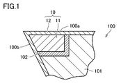
- FIG. 1 is a partial cross-sectional view showing an example of the configuration of a cutting tool according to the present embodiment.
- FIG. 2 is a TEM image (bright-field image) of 2 million times showing the interface between cubic boron nitride and the coating in FIG.
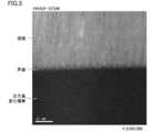
- FIG. 2 is a 2 million times TEM image (HAADF image (high-angle annular dark field image)) showing the interface between the cubic boron nitride and the coating in FIG.
- HAADF image high-angle annular dark field image
- the present disclosure provides a surface-coated cubic boron nitride sintered body excellent in peeling resistance of a coating and a cutting tool including the same.
- M to N means the upper and lower limits of the range (that is, not less than M and not more than N), and there is no unit in M, but only in N.
- the unit of M and the unit of N are the same.
- a surface-coated cubic boron nitride sintered body includes a base material that is a cubic boron nitride sintered body and a coating that covers the base material in contact with the base material.
- the Fe content is 1 at% or less
- the W content is 1 at% or less
- the O content is 2 at% or less.
- the cubic boron nitride sintered body as a base material is composed of cubic boron nitride and a binder.
- the adhesion between the substrate and the coating is affected by the difference in lattice constant between the cubic boron nitride crystal and the coating crystal in the substrate.
- the lattice constant of the crystal of the coating is larger than the lattice constant of the cubic boron nitride crystal.
- at least one of Fe and W is present at the interface, it penetrates into the crystal of the film, and increases the lattice constant of the crystal.
- Fe is often contained in a jig used when forming a film, and tends to adhere to the surface of the substrate.
- the base material is brazed to a cemented carbide obtained by sintering WC powder. Therefore, when a film is formed on the surface of the substrate after being brazed to the cemented carbide, W contained in the cemented carbide tends to adhere to the surface of the substrate.
- the lattice constant of the crystal increases due to the entry of Fe or W into the crystal of the coating, and the adhesion between the substrate and the coating tends to decrease.
- the adhesion between the cubic boron nitride and the coating is improved, and a surface-coated cubic boron nitride sintered body having improved peeling resistance of the coating can be realized.
- the thickness of the layer having a total content of Fe content and W content of 0.05 at% or more is 5 nm or less.
- the coating is a polycrystalline body.
- a region within 10 nm from the interface in the coating consists of crystal grains having an average grain size of 10 nm or less.
- region in a film increases, the stress which arises in an interface can be relieve
- the increase in grain boundaries enhances the action of preventing the plastic deformation and the progress of cracks at the grain boundaries. Further, even when subjected to an impact, the coating is difficult to peel off, and the impact resistance of the surface-coated cubic boron nitride sintered body is improved.
- the Ar content at the interface is 1 at% or less.
- a cleaning process is performed by irradiating the surface of the substrate with Ar ions.
- Ar may adhere to the surface of the substrate and remain at the interface between the substrate and the coating.
- the crystallinity of the coating is deteriorated and the stress at the interface is increased, whereby the adhesion between the substrate and the coating is lowered.
- Ar content in an interface is 1 at% or less, the adhesiveness of a base material and a film improves.
- the thickness of the coating is not less than 0.3 ⁇ m and not more than 10 ⁇ m.
- the coating is at least one element selected from the group consisting of Al, Ti, Cr and Si, and at least selected from the group consisting of C and N It contains at least one compound composed of one element. Thereby, the hardness, abrasion resistance, and oxidation resistance of the coating are improved.
- a cutting tool according to the present disclosure includes the surface-coated cubic boron nitride sintered body. According to the said cutting tool, the peeling resistance of a film improves. Thereby, the lifetime of the cutting tool can be prolonged.
- the present embodiment an embodiment of the present invention (hereinafter referred to as “the present embodiment”) will be described. However, this embodiment is not limited to these.
- the same reference numerals represent the same or corresponding parts.
- the atomic ratio when a compound or the like is represented by a chemical formula, when the atomic ratio is not particularly limited, it includes any conventionally known atomic ratio, and is not necessarily limited to a stoichiometric range.
- FIG. 1 is a partial cross-sectional view showing an example of the configuration of a cutting tool according to the present embodiment.
- the cutting tool 100 includes a base metal 101 and a surface-coated cBN sintered body 10 fixed to a predetermined region of the base metal 101 via a brazing layer 102.
- the shape and application of the cutting tool 100 are not particularly limited.
- a pin for pin milling of a shaft can be exemplified.
- the shape and material of the base metal 101 are not particularly limited, and conventionally known ones can be used.
- the base metal 101 is a cemented carbide obtained by mixing and sintering WC (tungsten carbide) and a binder (for example, Co).
- the surface-coated cBN sintered body 10 includes a base material 11 and a coating 12 that contacts the base material 11 and covers the base material 11.
- the base material 11 is fixed to the base metal 101 via the brazing layer 102.
- the material for the brazing layer (the brazing material) may be appropriately selected in consideration of the bonding strength and the melting point, and a material having a melting point of 800 ° C. or higher (for example, a material mainly composed of Ag) is preferable.
- the coating 12 covers the surface of the base material 11 and extends to the surface of the base metal 101, and constitutes a rake face 100 a and a flank face 100 b of the cutting tool 100.
- the coating 12 preferably covers the entire surface of the substrate 11, but even if a part of the substrate 11 is not covered with the coating 12 or the configuration of the coating 12 is partially different. It does not depart from the scope of the present invention.
- the base material 11 is a cBN sintered body containing cBN and a binder.
- the cBN sintered body may contain other components as long as it contains cBN and a binder, and may contain unavoidable impurities due to raw materials used, production conditions, and the like.
- the cBN is contained in the cBN sintered body, for example, 40 to 75% by volume.
- the binding material is not particularly limited as long as it exhibits an action of binding cBNs to each other, and any conventionally known binding material can be adopted.
- the binding material includes a group 4 element (Ti, Zr, Hf, etc.), a group 5 element (V, Nb, Ta, etc.) and a group 6 element (Cr, Mo, W, etc.) of the periodic table of elements.
- a compound containing at least one of these elements and at least one element of C, N, B, and O, a solid solution of such a compound, or an aluminum compound is preferable.
- the binding material may include two or more of the above compounds, solid solutions of the above compounds, and aluminum compounds.
- the coating 12 is a polycrystal.
- the coating 12 is formed by a physical vapor deposition method directly on the substrate 11 and covers the substrate 11 in contact with the substrate 11.
- the film 12 is, for example, at least one compound selected from at least one element selected from the group consisting of Al, Ti, Cr and Si and at least one element selected from the group consisting of C and N including. Examples of the compound include TiAlN, AlCrN, TiAlSiN, TiSiN, TiCN and the like.
- the thickness of the coating 12 is preferably 0.3 to 10 ⁇ m. Thereby, the effect by a film can be exhibited notably. Such effects include improvements in hardness, wear resistance, oxidation resistance, reaction resistance, and chipping resistance. If the thickness of the coating 12 is less than 0.3 ⁇ m, these effects may not be sufficiently exhibited. If the thickness exceeds 10 ⁇ m, chipping tends to occur due to residual stress in the coating 12.
- the lower limit of the thickness of the film 12 is more preferably 0.5 ⁇ m, and even more preferably 1 ⁇ m.
- the upper limit of the thickness of the film 12 is more preferably 8 ⁇ m, still more preferably 6 ⁇ m, and particularly preferably 4 ⁇ m.
- a thin film of one layer or two or more layers may be formed on the surface of the film 12 as the second film.
- examples of such a thin film include a film having a material of any one of nitrides, carbides, carbonitrides and oxides of group 4 elements.
- the Fe content and W content are subjected to structural observation and elemental analysis of the fracture surface of the surface-coated cBN sintered body 10 using an energy dispersive X-ray analyzer (EDS) attached to a transmission electron microscope (TEM). Is measured. Specifically, a line crossing the interface is specified along the normal direction of the interface between the cubic boron nitride and the coating 12 in the base material 11 in the TEM image, and along the line using EDS. Line scan measurement to measure the concentration distribution change of the selected element.
- the interface between the cubic boron nitride and the coating 12 is a position where the concentration of B contained in the cubic boron nitride is 1 ⁇ 2 of the average value in the substrate 11.
- Fe and W are metallic elements (foreign metal elements) not included in the elements constituting the cubic boron nitride and the coating 12, and when detected at the interface, they are concentrated near the interface. A large amount of Fe is contained in a jig used when the coating 12 is formed. W is included in the base metal 101 when the base metal 101 is made of a cemented carbide containing WC. Therefore, Fe released from the jig and W released from the base metal 101 adhere to the surface of the base material 11 and are likely to remain at the interface between the base material 11 and the coating 12.
- a peak occurs in the concentration distribution of Fe obtained by line scan measurement.
- the peak includes a point corresponding to the interface on the line.
- the maximum concentration (at%) of the peak is the Fe content at the interface.
- the content of W at the interface is determined by the same method.
- the Fe content at the interface is more preferably 0.5 at% or less, and further preferably 0.3 at% or less.
- the W content at the interface is more preferably 0.5 at% or less, and further preferably 0.3 at% or less.
- the lower limit of the content of Fe and W at the interface is not particularly limited, and is ideally 0 at%.
- the oxygen (O) content (at%) at the interface between the cubic boron nitride and the coating 12 in the substrate 11 is 2 at% or less.
- the O content at the interface is measured by the same method as for Fe and W. However, when O is not concentrated near the interface, no peak occurs in the O concentration distribution obtained by EDS line scan measurement. In this case, the average value of the O content (at%) in the total 4 nm section of 2 nm from the interface to the film 12 side and 2 nm to the cubic boron nitride side is obtained as the O content of the interface.
- O at the interface between cubic boron nitride and coating 12 exists as an oxide. Such an oxide reduces the adhesion between the cubic boron nitride and the coating 12.
- O content (at%) at the interface between the cubic boron nitride and the coating 12 as described above, the adhesion between the cubic boron nitride and the coating 12 is reduced due to the oxide at the interface. And the peel resistance of the coating 12 can be improved.
- the O content at the interface is more preferably 1 at% or less, still more preferably 0.5 at% or less, and particularly preferably 0.3 at% or less.
- the lower limit of the O content (at%) at the interface is not particularly limited, but is preferably less than the detection limit of EDS, and ideally 0 at%.
- the thickness of the layer (hereinafter also referred to as “different metal element layer”) having a total content of Fe content and W content of 0.05 at% or more is preferably 5 nm or less.
- the thickness of the different metal element layer is determined based on the analysis result using the EDS attached to the TEM described above. Specifically, in the synthetic data of the concentration distribution of Fe and W obtained by the EDS line scan measurement, the line length at which the total content is 0.05 at% or more is obtained as the thickness of the different metal element layer. .
- the thickness of the different metal element layer is 5 nm or less, a decrease in adhesion due to at least one of Fe and W can be suppressed, and the adhesion between the cubic boron nitride and the coating 12 is further improved.
- the thickness of the different metal element layer is more preferably 3 nm or less, still more preferably 2 nm or less, and particularly preferably 1 nm or less.
- the lower limit of the thickness of the different metal element layer is not particularly limited, and is ideally 0 nm.
- the Ar content at the interface between the cubic boron nitride and the coating 12 is preferably 1 at% or less, more preferably 0.5 at% or less, and further preferably 0.3 at% or less.
- the surface of the base material 11 is usually irradiated with Ar ions for cleaning. Therefore, Ar ions are likely to adhere to the surface of the substrate 11 and remain at the interface between the cubic boron nitride and the coating 12.
- the Ar ions remaining at the interface also deteriorate the crystallinity of the interface in the coating film and increase the stress, so that the adhesion between the cubic boron nitride and the coating film 12 tends to decrease.
- the adhesiveness between the cubic boron nitride and the coating 12 can be further improved by defining the Ar content at the interface as described above. Similar to Fe and W, the Ar content (at%) at the interface is obtained by analysis using EDS attached to TEM.
- the lower limit of the Ar content at the interface is not particularly limited, and is ideally 0 at%.
- the region within 10 nm from the interface in the coating 12 is preferably composed of crystal grains having an average grain size of 10 nm or less. Thereby, a grain boundary increases in the vicinity of the interface in the coating 12. As a result, the stress generated from the difference in lattice constant between the cubic boron nitride crystal constituting the base material 11 and the crystal constituting the coating film 12 is easily relaxed by the grain boundary, and the peeling resistance of the coating film 12 is further improved. it can. In addition, the increase in grain boundaries enhances the action of preventing the plastic deformation and the progress of cracks at the grain boundaries.
- the average grain size of the crystal grains in a region within 10 nm from the interface in the coating 12 is more preferably 5 nm or less, and even more preferably 3 nm or less.
- the average particle size is preferably 1 nm or more in consideration of crystallinity.
- the manufacturing method of the cutting tool of the present embodiment includes, for example, a step of preparing a base material (hereinafter referred to as “base material preparation step”), a step of cleaning the surface of the base material (hereinafter referred to as “bombarding step”), And a step of forming a film on the surface of the substrate (hereinafter referred to as “film formation step”). Furthermore, the manufacturing method of a cutting tool is provided with the 1st pre-processing process implemented before a bombarding process, and the 2nd pre-processing process implemented before a film-forming process. Hereinafter, each process is explained in full detail.
- Base material preparation process the base material which is a cBN sintered compact is produced using a well-known method.
- a base material is produced by sintering a mixture of cBN particles and raw material powder of a binder under high temperature and high pressure.
- the cutting tool (however, it does not have a film) whose cutting-blade part consists of a base material is obtained.
- First pretreatment process The joined body of the base metal and the base material obtained in the base material preparation step is installed in a chamber of a PVD (Physical Vapor Deposition) apparatus, and the inside of the chamber is evacuated to a vacuum by a vacuum pump. At this time, it is preferable to heat the substrate to, for example, 650 ° C. in order to reduce the influence of outgas (outgas) in the chamber.
- PVD Physical Vapor Deposition
- the pressure in the chamber is reduced to 1 ⁇ 10 ⁇ 3 Pa or less, preferably 5 ⁇ 10 ⁇ 4 Pa or less.
- the moisture pressure in the chamber is measured when the chamber is depressurized.
- the moisture pressure in the chamber is more preferably 1 ⁇ 10 ⁇ 4 Pa or less, and further preferably 5 ⁇ 10 ⁇ 5 Pa or less.
- the lower limit of the moisture pressure in the chamber is not particularly limited, but can be easily lowered to about 1 ⁇ 10 ⁇ 5 Pa by using a vacuum pump.
- a gas purification device may be connected to the chamber, and the moisture pressure in the chamber may be controlled in combination with a vacuum pump.
- the gas purification device is a device that removes water using a catalyst or an adsorbent. By using the gas purifier, the water pressure in the chamber can be easily lowered to about 1 ⁇ 10 ⁇ 6 Pa.
- An inert gas is introduced into a chamber whose moisture pressure is limited to 1 ⁇ 10 ⁇ 3 Pa or less, a bias voltage is applied to the substrate, and the surface of the substrate is irradiated with inert gas ions. Thereby, impurities such as oxides are removed from the surface of the substrate, and the surface of the substrate is cleaned.
- Ar ions can be used as the inert gas ions.
- the substrate is irradiated with inert gas ions until the water pressure in the chamber becomes 5 ⁇ 10 ⁇ 3 Pa or less (preferably 3 ⁇ 10 ⁇ 3 Pa or less).
- the moisture pressure in the chamber is measured in a state where an inert gas is contained in the chamber.
- the moisture pressure in the chamber is more preferably 5 ⁇ 10 ⁇ 4 Pa or less, and further preferably 2 ⁇ 10 ⁇ 4 Pa or less.
- the bias voltage applied to the substrate is -100 to -300V.
- a high bias voltage condition for example, ⁇ 500 V
- the inert gas ions collide with the base metal and various jigs in the chamber.
- Metal particles for example, Fe, W
- a phenomenon resputtering
- the absolute value of the bias voltage to 300 V or less as described above, it is possible to suppress the metal particles released from the base metal and the jig from adhering to the substrate surface. Furthermore, it can suppress that an inert gas ion remains on the base-material surface.
- the irradiation energy to the base material of an inert gas ion reduces by making the absolute value of a bias voltage 300V or less, since the moisture pressure in a chamber is maintained in the low state as mentioned above, Oxidation on the surface of cubic boron nitride can be sufficiently suppressed.
- the absolute value of the bias voltage is set to 100V or more.
- the inert gas in the chamber is 0.6-1 Pa. Thereby, it can suppress that an inert gas ion remains on the base-material surface.
- Second pretreatment process >> Next, the inert gas is exhausted from the chamber by operating the vacuum pump. Thereafter, the process waits until the water pressure in the chamber becomes 2 ⁇ 10 ⁇ 4 Pa or less, preferably 1 ⁇ 10 ⁇ 4 Pa. At this time, the substrate is heated to 500 ° C. or higher.
- the moisture pressure in the chamber is more preferably 3 ⁇ 10 ⁇ 5 or less, and further preferably 2 ⁇ 10 ⁇ 5 or less.
- ⁇ Film formation process After the moisture pressure in the chamber becomes 2 ⁇ 10 ⁇ 4 Pa or less, a film is formed on the substrate surface by physical vapor deposition. Any conventionally known method (such as an arc ion plating method or a sputtering method) can be employed as the physical vapor deposition method.
- a film in the arc ion plating method, can be formed using a target (metal evaporation source) containing a metal species that constitutes the film and a reactive gas such as CH 4 or N 2 .
- a target metal evaporation source
- a reactive gas such as CH 4 or N 2 .
- a film can be formed by using a target including a metal species constituting the film, a reactive gas such as CH 4 or N 2, and a sputtering gas such as Ar, Kr, or Xe.
- a target including a metal species constituting the film, a reactive gas such as CH 4 or N 2, and a sputtering gas such as Ar, Kr, or Xe.
- a sputtering gas such as Ar, Kr, or Xe.
- HiPIMS method high power ion pulse magnetron sputtering method
- the metal atoms, O, and inert gas ions contained in the jig or base metal on the substrate surface are suppressed from adhering to the substrate surface.
- the content of these atoms at the interface can be reduced.
- nucleation and grain growth occur uniformly during film formation, the grain boundary near the interface in the coating increases, and the stress generated at the interface can be relaxed. As a result, the adhesion between the cubic boron nitride and the coating is improved, and the peeling resistance of the coating is improved.
- the cutting tools 1 to 9 and 12 to 15 include the above-described surface-coated cBN sintered body.
- the cutting tools 10 and 11 are comparative examples.
- Example No. 1 cutting tool> A mixture of 70% by volume of cBN and the remaining binder (TiN, Ti, Al) was sintered at 1400 ° C. and 5 Pa to prepare a base material that was a cBN sintered body. This sintered body was bonded to a base metal made of a WC-based cemented carbide and formed into the shape of ISO standard DNGA150408. For joining, a brazing material containing Ag as a main component was used.
- the joined body of the base material and the base metal was installed in the chamber of the PVD apparatus using the HiPIMS method.
- a vacuum pump is connected to the chamber of the PVD apparatus, and the inside of the chamber can be evacuated.
- a turntable is installed in the chamber, and the turntable is configured so that a joined body including a base material can be set via a jig.
- the base material set in the chamber can be heated by a heater installed in the chamber.
- a gas pipe for introducing gas used in the bombarding process and the film forming process is connected to the chamber via a mass flow controller (MFC) for flow rate control.
- MFC mass flow controller
- a tungsten filament for generating Ar ions for the bombarding process and a sputtering source for the film forming process to which a necessary power source is connected are arranged.
- An evaporation source material (target) necessary for film formation can be set in the sputtering source.
- the substrate While evacuating the inside of the chamber with a vacuum pump, the substrate was heated at 650 ° C. for 2 hours with a heater installed in the chamber. Thereafter, heating and evacuation were continued until the water pressure in the chamber became 1 ⁇ 10 ⁇ 3 Pa or less.
- the moisture pressure in the chamber was measured using a gas analyzer “Qulee CGM-052” manufactured by ULVAC, Inc.
- the water pressure in the chamber was measured, and the bombardment was continued until the water pressure became 5 ⁇ 10 ⁇ 3 Pa or less.
- the water pressure at the end of the bombardment was 4.92 ⁇ 10 ⁇ 3 Pa.
- the moisture pressure in the bombardment was measured with Ar gas in the chamber.
- water pressure at the start of film formation was 1.94 ⁇ 10 ⁇ 4 Pa.
- Sample No. 1 was used except that an arc ion plating method was used for forming the coating and the film forming process was performed according to the following film forming conditions. Sample No. 1 under the same conditions as in No. 1. 14 cutting tools were produced.
- Sample No. For each of the cutting tools 1 to 15, samples for analysis were prepared that were broken in the direction perpendicular to the interface between the substrate and the coating. The fracture surface is smoothed by irradiation with a focused ion beam, and then analyzed by an ion milling apparatus using an Ar ion beam so that the thickness along the normal direction of the fracture surface is 100 nm. The fracture surface of the sample was polished. This is to suppress variation in the measured value of the O content due to the thickness of the analytical sample.
- the sample was introduced into a TEM apparatus to obtain a TEM image near the interface between the cubic boron nitride and the coating, Line scan measurement by EDS was performed so as to cross the interface with the coating. The following was used as an analyzer.
- a 200 nm long line is specified that crosses the interface along the normal direction of the interface between the cubic boron nitride and the coating, and the concentration distribution of elements along the line is determined using EDS.
- a line scan measurement was performed to measure the change.
- the measurement elements were Fe, W, O, and Ar in addition to B and N, which are calibration elements of cubic boron nitride, and the constituent elements of the film.
- B and N which are calibration elements of cubic boron nitride, and the constituent elements of the film.
- concentration in a base material was specified as a point on an interface.
- the concentrations of elements other than B and N detected in cubic boron nitride are the background level (detection limit) in the measurement, and the respective concentrations of these elements in cubic boron nitride.
- the average values of these were calculated, these values were excluded from the line scan measurement results, and the concentrations of the measured elements were recalculated.
- the maximum concentration of Fe and W concentration distribution peaks (peaks including points on the interface) in the vicinity of the interface in the recalculated line scan measurement results was defined as the Fe (W) content (at%) at the interface.
- Sample No. In 1 to 15 cutting tools, at least one of Fe and W was detected at the interface.
- the O content (at%) at the interface was evaluated from the line scan measurement result using EDS.
- the maximum concentration of the peak was defined as the O content (at%) at the interface, similarly to Fe and W.
- the average of the O content (at%) in the total 4 nm section of 2 nm from the interface to the film side and 2 nm to the cubic boron nitride side was defined as the O content (at%) at the interface.
- ⁇ Average particle size of the coating near the interface> In a 5 million times TEM image, the average grain size of the crystal grains at a position of 10 nm from the interface in the coating was measured. Specifically, a lattice image is taken in a high-resolution TEM image, crystal grains are distinguished by the difference in crystal orientation and the presence of grain boundaries, the width of 30 crystal grains is measured for one sample, and the average value is calculated. The average particle size was taken.
- the cutting edge portion was cut out by wire electric discharge machining, and the cut out portion was embedded in resin. Thereafter, the cross section of the coating was exposed by CP (cross section polisher) processing based on the ion milling method, and an SEM image at a magnification of 15000 was observed. The film thickness was measured at five points in a region within 1 mm from the tip of the blade edge, and an average value was taken.
- Table 2 shows Sample No. For each of the cutting tools 1 to 15, the content at the interface of Fe and W, the content of O and Ar at the interface, the thickness of the different metal element layer, and the average particle diameter at a position 10 nm from the interface in the coating film The measurement result of the thickness of a film and a tool life is shown.
- FIG. 2 shows sample no. 2 is a TEM image (bright-field image) of 2 million times showing the interface between cubic boron nitride and the coating in FIG.
- FIG. 2 is a 2 million times TEM image (HAADF image (high-angle annular dark field image)) showing the interface between the cubic boron nitride and the coating in FIG.
- HAADF image high-angle annular dark field image
- the Fe content at the interface is 1 at% or less and the W content is 1 at% or less, it is possible to suppress an increase in the lattice constant of the crystal in the coating film due to Fe and W entering the crystal of the coating film.
- an increase in the difference in lattice constant between the cubic boron nitride crystal and the coating crystal in the substrate can be suppressed, and the adhesion between the cubic boron nitride and the coating is improved.
- the O content at the interface between the cubic boron nitride and the coating is suppressed to 2 at% or less, and the decrease in adhesion between the cubic boron nitride and the coating due to O can be suppressed.
- the adhesion between the cubic boron nitride and the coating is improved. It is considered that the peel resistance of the coating in the cutting tools 1 to 9 and 12 to 15 was improved.
- sample no. With 10 cutting tools, it was confirmed that the tool life was as short as 2 minutes.
- Sample No. 10 the moisture pressure before the start of bombardment is 1.98 ⁇ 10 ⁇ 3 Pa, and the moisture pressure at the end of bombardment is 7.93 ⁇ 10 ⁇ 3 Pa. Therefore, at the interface between the cubic boron nitride and the coating, The O content (at%) is higher than 2 at%. As a result, it is considered that the adhesion between the cubic boron nitride and the coating is lowered, and the tool life is shortened.
Landscapes
- Engineering & Computer Science (AREA)
- Chemical & Material Sciences (AREA)
- Mechanical Engineering (AREA)
- Ceramic Engineering (AREA)
- Materials Engineering (AREA)
- Structural Engineering (AREA)
- Organic Chemistry (AREA)
- Inorganic Chemistry (AREA)
- Crystallography & Structural Chemistry (AREA)
- Manufacturing & Machinery (AREA)
- Physical Vapour Deposition (AREA)
- Cutting Tools, Boring Holders, And Turrets (AREA)
Abstract
La présente invention concerne un corps fritté de nitrure de bore cubique revêtu en surface comprenant un substrat, qui se présente sous la forme d'un corps fritté de nitrure de bore cubique, et un film de revêtement qui entre en contact avec le substrat et qui recouvre ce dernier. Au niveau de l'interface entre le nitrure de bore cubique dans le substrat et le film de revêtement, la teneur en Fe est inférieure ou égale à 1 % at, la teneur en W est inférieure ou égale à 1 % at, et la teneur en O est inférieure ou égale à 2 % at.
Priority Applications (1)
| Application Number | Priority Date | Filing Date | Title |
|---|---|---|---|
| JP2019521955A JP7016866B2 (ja) | 2017-05-29 | 2018-02-21 | 表面被覆立方晶窒化硼素焼結体およびこれを備える切削工具 |
Applications Claiming Priority (2)
| Application Number | Priority Date | Filing Date | Title |
|---|---|---|---|
| JP2017-105583 | 2017-05-29 | ||
| JP2017105583 | 2017-05-29 |
Publications (1)
| Publication Number | Publication Date |
|---|---|
| WO2018220910A1 true WO2018220910A1 (fr) | 2018-12-06 |
Family
ID=64454509
Family Applications (1)
| Application Number | Title | Priority Date | Filing Date |
|---|---|---|---|
| PCT/JP2018/006170 Ceased WO2018220910A1 (fr) | 2017-05-29 | 2018-02-21 | Corps fritté de nitrure de bore cubique revêtu en surface et outil de coupe doté de ce dernier |
Country Status (2)
| Country | Link |
|---|---|
| JP (1) | JP7016866B2 (fr) |
| WO (1) | WO2018220910A1 (fr) |
Cited By (1)
| Publication number | Priority date | Publication date | Assignee | Title |
|---|---|---|---|---|
| JP2021053740A (ja) * | 2019-09-30 | 2021-04-08 | 株式会社タンガロイ | 被覆工具 |
Citations (2)
| Publication number | Priority date | Publication date | Assignee | Title |
|---|---|---|---|---|
| JP2010029980A (ja) * | 2008-07-29 | 2010-02-12 | Kyocera Corp | 切削工具 |
| JP2015209354A (ja) * | 2014-04-25 | 2015-11-24 | 住友電工ハードメタル株式会社 | 複合焼結体および表面被覆窒化硼素焼結体工具 |
Family Cites Families (3)
| Publication number | Priority date | Publication date | Assignee | Title |
|---|---|---|---|---|
| US8178220B2 (en) * | 2004-04-30 | 2012-05-15 | Sumitomo Electric Hardmetal Corp. | Surface-covered cubic boron nitride sintered body tool and method of manufacturing the same |
| EP2778146B1 (fr) * | 2011-11-07 | 2018-05-09 | Tungaloy Corporation | Corps fritté en nitrure de bore cubique |
| JP2015209534A (ja) * | 2014-04-30 | 2015-11-24 | 株式会社日本触媒 | (ポリ)アルキレングリコール化合物及び(ポリ)アルキレングリコール系重合体 |
-
2018
- 2018-02-21 WO PCT/JP2018/006170 patent/WO2018220910A1/fr not_active Ceased
- 2018-02-21 JP JP2019521955A patent/JP7016866B2/ja active Active
Patent Citations (2)
| Publication number | Priority date | Publication date | Assignee | Title |
|---|---|---|---|---|
| JP2010029980A (ja) * | 2008-07-29 | 2010-02-12 | Kyocera Corp | 切削工具 |
| JP2015209354A (ja) * | 2014-04-25 | 2015-11-24 | 住友電工ハードメタル株式会社 | 複合焼結体および表面被覆窒化硼素焼結体工具 |
Cited By (2)
| Publication number | Priority date | Publication date | Assignee | Title |
|---|---|---|---|---|
| JP2021053740A (ja) * | 2019-09-30 | 2021-04-08 | 株式会社タンガロイ | 被覆工具 |
| JP7467860B2 (ja) | 2019-09-30 | 2024-04-16 | 株式会社タンガロイ | 被覆工具 |
Also Published As
| Publication number | Publication date |
|---|---|
| JPWO2018220910A1 (ja) | 2020-03-26 |
| JP7016866B2 (ja) | 2022-02-07 |
Similar Documents
| Publication | Publication Date | Title |
|---|---|---|
| KR102268364B1 (ko) | 표면 피복 절삭 공구 및 그 제조 방법 | |
| JP6773287B2 (ja) | 表面被覆工具およびその製造方法 | |
| JP5297388B2 (ja) | 表面被覆切削工具 | |
| JP5098726B2 (ja) | 被覆工具及び被覆工具の製造方法 | |
| KR102198744B1 (ko) | 표면 피복 절삭 공구 | |
| JP5321975B2 (ja) | 表面被覆切削工具 | |
| EP3808477B1 (fr) | Outil de coupe à revêtement de surface et son procédé de production | |
| KR20190142359A (ko) | 피복 절삭 공구 | |
| JPWO2019171648A1 (ja) | 表面被覆切削工具及びその製造方法 | |
| JP6984108B2 (ja) | 表面被覆切削工具及びその製造方法 | |
| JP7016866B2 (ja) | 表面被覆立方晶窒化硼素焼結体およびこれを備える切削工具 | |
| JPWO2020075356A1 (ja) | 切削工具及びその製造方法 | |
| JP7055961B2 (ja) | 表面被覆切削工具及びその製造方法 | |
| JP7064438B2 (ja) | 切削工具およびその製造方法 | |
| JP6122975B2 (ja) | TixSi1−xN層を含んでなるコーティングによりワークピースをコーティングする方法 | |
| JP2012076156A (ja) | 超硬合金およびその製造方法 | |
| JP4697389B2 (ja) | 高速切削加工で硬質被覆層がすぐれた耐摩耗性を発揮する表面被覆超硬合金製切削工具 | |
| JP5327534B2 (ja) | 硬質被覆層の耐欠損性、耐剥離性に優れる表面被覆切削工具 | |
| JP2017166011A (ja) | 被膜、切削工具および被膜の製造方法 | |
| JP7286812B2 (ja) | 切削工具 | |
| JP2006015451A (ja) | 高速切削加工で硬質被覆層がすぐれた耐摩耗性を発揮する表面被覆超硬合金製切削工具の製造方法 | |
| JP2020152983A (ja) | 被覆切削工具及びその製造方法 | |
| JPH08174341A (ja) | 硬質膜被覆ツイストドリルおよびその製造方法 | |
| JP2005342856A (ja) | 断続重切削条件で硬質被覆層がすぐれた耐チッピング性を発揮する表面被覆超硬合金製切削工具 |
Legal Events
| Date | Code | Title | Description |
|---|---|---|---|
| 121 | Ep: the epo has been informed by wipo that ep was designated in this application |
Ref document number: 18810802 Country of ref document: EP Kind code of ref document: A1 |
|
| ENP | Entry into the national phase |
Ref document number: 2019521955 Country of ref document: JP Kind code of ref document: A |
|
| NENP | Non-entry into the national phase |
Ref country code: DE |
|
| 122 | Ep: pct application non-entry in european phase |
Ref document number: 18810802 Country of ref document: EP Kind code of ref document: A1 |