WO2018230116A1 - 磁気センサ及び磁気センサの製造方法 - Google Patents
磁気センサ及び磁気センサの製造方法 Download PDFInfo
- Publication number
- WO2018230116A1 WO2018230116A1 PCT/JP2018/014689 JP2018014689W WO2018230116A1 WO 2018230116 A1 WO2018230116 A1 WO 2018230116A1 JP 2018014689 W JP2018014689 W JP 2018014689W WO 2018230116 A1 WO2018230116 A1 WO 2018230116A1
- Authority
- WO
- WIPO (PCT)
- Prior art keywords
- magnetic
- layer
- thin film
- film magnet
- magnetic sensor
- Prior art date
- Legal status (The legal status is an assumption and is not a legal conclusion. Google has not performed a legal analysis and makes no representation as to the accuracy of the status listed.)
- Ceased
Links
Images

Classifications
-
- G—PHYSICS
- G01—MEASURING; TESTING
- G01R—MEASURING ELECTRIC VARIABLES; MEASURING MAGNETIC VARIABLES
- G01R33/00—Arrangements or instruments for measuring magnetic variables
- G01R33/02—Measuring direction or magnitude of magnetic fields or magnetic flux
- G01R33/06—Measuring direction or magnitude of magnetic fields or magnetic flux using galvano-magnetic devices
- G01R33/063—Magneto-impedance sensors; Nanocristallin sensors
-
- G—PHYSICS
- G01—MEASURING; TESTING
- G01R—MEASURING ELECTRIC VARIABLES; MEASURING MAGNETIC VARIABLES
- G01R33/00—Arrangements or instruments for measuring magnetic variables
- G01R33/0052—Manufacturing aspects; Manufacturing of single devices, i.e. of semiconductor magnetic sensor chips
Definitions
- the present invention relates to a magnetic sensor and a method for manufacturing the magnetic sensor.
- a thin film magnet made of a hard magnetic film formed on a nonmagnetic substrate, an insulating layer covering the thin film magnet, and uniaxial anisotropy formed on the insulating layer are provided.
- a magnetic sensing part made of one or a plurality of rectangular soft magnetic films, and a conductor film electrically connecting the plurality of soft magnetic films of the magnetic sensing part, and the longitudinal direction of the magnetic sensing part In the direction, both end portions of the thin film magnet are located outside both end portions of the magnetosensitive portion, and the insulating layer has an opening on each end portion of the thin film magnet,
- a yoke portion made of a soft magnetic film that forms a magnetic path between the thin film magnet and the magnetic sensing portion is formed from an end portion of the thin film magnet through an opening of the insulating layer.
- a bias magnetic field is applied to the magneto-impedance effect element so that the impedance of the magneto-impedance effect element changes linearly with respect to a change in the external magnetic field.
- a method for generating the bias magnetic field there is a method using a thin film magnet.
- a thin film magnet By using a thin film magnet, it is not necessary to provide a coil for generating a magnetic field.
- Such a thin film magnet is required to have magnetic anisotropy in the in-plane direction.
- the present invention provides a magnetic sensor or the like in which a thin film magnet is likely to generate magnetic anisotropy in the in-plane direction as compared with a case where no control layer is used.
- a magnetic sensor to which the present invention is applied is composed of a hard magnetic material, is composed of a thin film magnet having magnetic anisotropy in the in-plane direction, and a soft magnetic material, and is disposed opposite to the thin film magnet, and has a longitudinal direction. And a short direction, the longitudinal direction is the direction through which the magnetic flux generated by the thin-film magnet is transmitted, and has uniaxial magnetic anisotropy in the direction intersecting the longitudinal direction, and is sensitive to changes in the magnetic field.
- a sensing unit including an element, and a control layer that is disposed on the opposite side of the thin film magnet from the side where the sensing element is provided and controls the magnetic anisotropy of the thin film magnet in an in-plane direction.
- the control layer has a bcc structure
- the hard magnetic body constituting the thin film magnet has an hcp structure
- the hard magnetic body is crystal-grown on the bcc structure of the control layer, so that c
- the axis is oriented in-plane.
- the control layer can be characterized by being Cr, Mo or W or an alloy containing them. By doing in this way, control of the orientation of the hard magnetic body which comprises a thin film magnet becomes easy.
- the control layer can be characterized in that it is disposed on a nonmagnetic substrate having a groove provided along a direction connecting both magnetic poles of the thin film magnet. By doing in this way, control of the orientation of the hard magnetic body which comprises a thin film magnet becomes easier.
- an adhesion layer for improving adhesion of the control layer to the substrate can be provided between the substrate and the control layer. By doing so, stability is improved.
- the sensitive element of the sensitive part may be characterized by comprising a plurality of soft magnetic layers that are antiferromagnetically coupled with a demagnetizing field suppressing layer made of Ru or Ru alloy interposed therebetween. By doing so, the magnetic impedance effect is improved.
- the sensing unit may include a plurality of sensing elements arranged in parallel, and the plurality of sensing elements may be configured to be connected in series with a connection member composed of a conductor. . By doing so, sensitivity is improved.
- a yoke provided so as to be opposed to the longitudinal end of the sensing element in the sensing part from the magnetic pole of the thin film magnet, and for guiding the magnetic flux generated by the thin film magnet to pass through the sensing element in the longitudinal direction.
- a bias magnetic field is effectively applied.
- the method of manufacturing a magnetic sensor to which the present invention is applied is a control for controlling the magnetic anisotropy of a hard magnetic layer formed on a non-magnetic substrate in an in-plane direction.
- a sensing part forming step of forming a sensing part comprising:
- the substrate in the control layer forming step may be a substrate in which grooves are formed along a direction connecting both magnetic poles of the thin film magnet.
- the present invention it is possible to provide a magnetic sensor or the like in which the thin film magnet is likely to generate magnetic anisotropy in the in-plane direction as compared with the case where the control layer is not used.
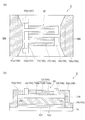
- (A) is a plan view, and (b) is a cross-sectional view taken along line IB-IB in (a). It is a figure explaining an example of the manufacturing method of a magnetic sensor.
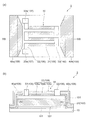
- 2A to 2G show steps in the method of manufacturing the magnetic sensor. It is a figure explaining an example of the magnetic sensor with which 2nd Embodiment is applied.
- (A) is a plan view, and (b) is a sectional view taken along line IIIB-IIIB in (a).
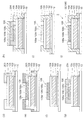
- 4D to 4J show steps in the method of manufacturing the magnetic sensor. It is a figure explaining an example of the magnetic sensor with which 3rd Embodiment is applied.
- (A) is a plan view, and (b) is a cross-sectional view taken along line VB-VB in (a).
- FIG. 1 is a diagram illustrating an example of a magnetic sensor 1 to which the first embodiment is applied.
- 1A is a plan view
- FIG. 1B is a cross-sectional view taken along line IB-IB in FIG. 1A.
- a magnetic sensor 1 to which the first embodiment is applied is opposed to a thin film magnet 20 made of a hard magnetic material (hard magnetic material layer 103) and the thin film magnet 20.
- a soft magnetic material soft magnetic material layer 105
- sensing a change in magnetic field external magnetic field
- the magnetic anisotropy of the thin-film magnet 20 is in the in-plane direction of the film.
- a control layer 102 that controls to develop is provided.
- the control layer 102 is provided on the opposite side of the thin film magnet 20 from the side on which the sensing part 30 is provided.
- the layers constituting the thin-film magnet 20, here, the hard magnetic layer 103 are described in parentheses. The same applies to other cases.
- the sensing unit 30 includes a plurality of strip-shaped sensing elements 31 having a longitudinal direction and a short-side direction, and ends of adjacent sensing elements 31 connected in series in a zigzag manner.
- a connection member 32 composed of a body (conductor layer 106) is provided.
- the plurality of sensing elements 31 are arranged in parallel in the longitudinal direction.
- a connecting member 32 is also provided at the end where there is no adjacent sensing element 31.
- the sensing unit 30 includes electrode pads 33a and 33b (conductors) for energization at both ends (the connection member 32 at the end where there is no adjacent sensing element 31) where the sensing element 31 is connected in series by the connection member 32.
- the sensing unit 30 includes four sensing elements 31 as an example. However, the sensing part 30 may be one or more than four.
- the sensitive element 31 is a magneto-impedance effect element.
- the magnetic sensor 1 has a magnetic flux generated from the N pole and the S pole of the thin film magnet 20 (indicated as (N) and (S) in FIG. 1B).
- the yoke 40a for inducing magnetic flux from the north pole of the thin film magnet 20 to one end in the longitudinal direction of the sensitive element 31 in the sensitive part 30 so as to pass through the sensitive element 31 of the sensitive part 30 in the longitudinal direction;
- a yoke 40b for inducing magnetic flux from the other end in the longitudinal direction of the sensing element 31 in the portion 30 to the south pole of the thin-film magnet 20.
- the yokes 40a and 40b are made of a soft magnetic material (soft magnetic material layer 105) through which magnetic flux easily passes. That is, the thin film magnet 20 applies a bias magnetic field to the sensing unit 30. Note that the N pole and S pole of the thin film magnet 20 are collectively referred to as both magnetic poles, and the N pole and S pole are referred to as magnetic poles if they are not distinguished.
- the magnetic sensor 1 is configured by arranging (stacking) an adhesion layer 101, a control layer 102, a thin film magnet 20 (hard magnetic layer 103), an insulating layer 104, and a sensing part 30 in this order on a nonmagnetic substrate 10. ing.
- the adhesion layer 101, the control layer 102, the thin film magnet 20 (hard magnetic layer 103), and the insulating layer 104 are processed so that at least two opposing side surfaces are exposed.
- the at least two side surfaces to be exposed are set such that the two side surfaces of the hard magnetic layer 103 constituting the exposed thin-film magnet 20 are an N pole and an S pole.
- the yokes 40a and 40b are provided in contact with the exposed north and south poles of the thin film magnet 20, respectively, and guide the magnetic flux so that it passes through the sensing element 31 in the longitudinal direction.
- the yokes 40a and 40b may not be provided in contact with the exposed north and south poles of the thin film magnet 20, and may have a gap (gap). If the yokes 40a and 40b are in contact with the north and south poles of the thin film magnet 20, the leakage of magnetic flux is suppressed.
- the yoke 40 (yokes 40 a and 40 b) is configured such that the shape viewed from the upper side of the substrate 10 becomes narrower as it approaches the sensing part 30. This is because the magnetic flux generated by the thin film magnet 20 is concentrated on the sensing unit 30 (the magnetic flux density is increased). That is, the width of the N pole and the S pole of the thin film magnet 20 is made wider than the width of the portion of the sensing unit 30 where the plurality of sensing elements 31 are provided, so that the bias magnetic field to the sensing unit 30 becomes strong. .
- the width of the portion of the yoke 40 (yoke 40a, 40b) facing the sensing portion 30 only needs to be set wider than the width of the portion of the sensing portion 30 where the plurality of sensing elements 31 are provided. Note that the width of the portion of the yoke 40 (yoke 40a, 40b) facing the sensing portion 30 need not be narrowed.
- the distance between the yoke 40 (yokes 40a and 40b) and the end of the sensing element 31 in the longitudinal direction of the sensing element 31 may be, for example, 1 ⁇ m to 100 ⁇ m.
- the substrate 10 is a substrate made of a non-magnetic material, and examples thereof include a semiconductor substrate such as silicon, and an oxide substrate such as sapphire and glass.
- the adhesion layer 101 improves the adhesion of the control layer 102 to the substrate 10.
- an alloy containing Cr or Ni is preferably used as the adhesion layer 101.
- the alloy containing Cr or Ni include CrTi, CrTa, NiTa and the like.
- the thickness of the adhesion layer 101 is, for example, 5 nm to 50 nm. If there is no problem with the adhesion of the control layer 102 to the substrate 10, it is not necessary to provide the adhesion layer 101. In the present specification, the composition ratio of the alloy is not particularly shown. The same applies hereinafter.
- the control layer 102 is a layer that controls the magnetic anisotropy of the thin-film magnet 20 composed of the hard magnetic layer 103 so as to develop in the in-plane direction of the film.
- As the control layer 102 Cr, Mo, W, or an alloy containing them (hereinafter, referred to as an alloy containing Cr or the like constituting the control layer 102) may be used.
- Examples of the alloy containing Cr and the like constituting the control layer 102 include CrTi, CrMo, CrV, and CrW.
- the thickness of the control layer 102 is, for example, 5 nm to 100 nm.
- the hard magnetic material (hard magnetic material layer 103) constituting the thin film magnet 20 is an alloy containing Co as a main component and containing either one or both of Cr and Pt (hereinafter referred to as a Co alloy constituting the thin film magnet 20). To be used). Examples of the Co alloy constituting the thin film magnet 20 include CoCrPt, CoCrTa, CoNiCr, and CoCrPtB. Note that Fe may be included.
- the thickness of the hard magnetic material (hard magnetic material layer 103) constituting the thin film magnet 20 is, for example, 50 nm to 500 nm.
- the alloy containing Cr or the like constituting the control layer 102 has a bcc (body-centered cubic) structure. Therefore, the hard magnetic material (hard magnetic material layer 103) constituting the thin-film magnet 20 is hcp (hexagonal close-packed) that is easy to grow crystals on the control layer 102 made of an alloy containing Cr or the like having a bcc structure. Close-packed))) structure.
- the hard magnetic layer 103 having the hcp structure is grown on the bcc structure, the ccp axis of the hcp structure is easily oriented in the plane. Therefore, the thin-film magnet 20 constituted by the hard magnetic layer 103 tends to have magnetic anisotropy in the in-plane direction.
- the hard magnetic layer 103 is polycrystalline, and each crystal has magnetic anisotropy in the in-plane direction. Therefore, this magnetic anisotropy is sometimes called crystal magnetic anisotropy.
- the substrate 10 is preferably heated to 100 ° C. to 600 ° C. in order to promote crystal growth of the alloy containing Cr or the like constituting the control layer 102 and the Co alloy constituting the thin film magnet 20.
- an alloy containing Cr or the like in the control layer 102 grows, and the hard magnetic layer 103 having the hcp structure is easily crystallized so that it has an axis of easy magnetization. That is, magnetic anisotropy is easily imparted in the plane of the hard magnetic layer 103.
- the insulating layer 104 is made of a nonmagnetic insulator and electrically insulates between the thin film magnet 20 and the sensing part 30.
- Examples of the insulator constituting the insulating layer 104 include oxides such as SiO 2 and Al 2 O, or nitrides such as Si 2 N 4 and AlN.
- the thickness of the insulating layer 104 is, for example, 100 nm to 500 nm.
- the sensing element 31 in the sensing unit 30 is given uniaxial magnetic anisotropy in a direction intersecting the longitudinal direction, for example, a direction orthogonal to the longitudinal direction (width direction).
- a Co alloy constituting the sensing element 31 an alloy containing Co as a main component (hereinafter referred to as a Co alloy constituting the sensing element 31) is used as a refractory metal Nb, Ta. , W or other amorphous alloy can be used.
- Examples of the Co alloy constituting the sensing element 31 include CoNbZr, CoFeTa, and CoWZr.
- the thickness of the soft magnetic material (soft magnetic layer 105) constituting the sensing element 31 is, for example, 0.5 ⁇ m to 5 ⁇ m.
- connection member 32 (conductor layer 106) and the electrode pad 33 (conductor layer 107) may be any conductor having excellent conductivity, and for example, Cu, Au, Al, or the like can be used.
- the yoke 40 (yoke 40a, 40b) is preferably composed of a soft magnetic material having a high magnetic permeability.
- the yoke 40 is composed of the soft magnetic layer 105 that constitutes the sensing element 31 of the sensing unit 30.
- the yoke 40 reduces magnetic flux leakage from the thin film magnet 20 and efficiently applies a bias magnetic field to the sensing unit 30 (sensing element 31).
- the thin film magnet 20 does not require a coil for generating a magnetic field. Therefore, power saving and size reduction of the magnetic sensor 1 can be achieved.
- the thin film magnet 20 may be provided as a plurality of thin film magnet pieces in the same manner as the sensing element 31 of the sensing unit 30, and the thin film magnet pieces may be provided corresponding to each sensing element 31. That is, the sensing element 31 may be laminated on the thin film magnet piece via the insulating layer 104. By doing so, the demagnetizing field generated inside the thin film magnet 20 is reduced, and the magnetic flux generation efficiency from the thin film magnet 20 is increased.
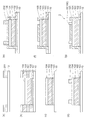
- FIG. 2 is a diagram illustrating an example of a method for manufacturing the magnetic sensor 1.
- 2A to 2G show steps in the method for manufacturing the magnetic sensor 1.
- FIG. 2A to 2G are typical steps, and the process proceeds in the order of FIGS. 2A to 2G.
- 2 (a) to 2 (g) correspond to the cross-sectional view of FIG. 1 (b).
- the substrate 10 is a substrate made of a nonmagnetic material, for example, a semiconductor substrate such as silicon or an oxide substrate such as sapphire or glass.
- the substrate 10 may be provided with a streak-like groove or streak-like unevenness having a radius of curvature Ra of 0.1 nm to 100 nm, for example, using a polishing machine.
- the direction of the streak-like grooves or streak-like uneven streaks is preferably provided in a direction connecting the N pole and the S pole of the thin-film magnet 20 constituted by the hard magnetic layer 103. By doing so, crystal growth in the hard magnetic layer 103 is promoted in the direction of the groove.
- the easy axis of magnetization of the thin film magnet 20 constituted by the hard magnetic layer 103 is more likely to be directed in the groove direction (direction connecting the N pole and the S pole of the thin film magnet 20). That is, magnetization of the thin film magnet 20 is made easier.
- the lift-off method is mainly used. Note that an etching method may be used.
- a pattern 201 is formed by known photolithography.
- the adhesion layer 101, the control layer 102, and the hard magnetic layer 103 constituting the thin film magnet 20 are sequentially formed on the surface of the substrate 10 on which the resist pattern 201 is formed. (accumulate. For example, using a sputtering method, an alloy layer (film) containing Cr or Ni to be the adhesion layer 101, an alloy layer (film) containing Cr or the like to be the control layer 102, and Co to be the hard magnetic layer 103 An alloy layer (film) is successively formed (deposited).
- the substrate 10 may be heated to, for example, 100 ° C. to 600 ° C. in order to promote crystal growth.
- the process of forming the control layer 102 is an example of the control layer forming process.
- the substrate 10 may or may not be heated in forming the adhesion layer 101. In order to remove moisture adsorbed on the substrate 10, the substrate 10 may be heated before the adhesion layer 101 is formed.
- the insulating layer 104 can be formed by plasma CVD, reactive sputtering, or the like.
- the portions deposited on the resist pattern 201 of the adhesion layer 101, the control layer 102, the hard magnetic layer 103, and the insulating layer 104 are removed. (Lift off). In this way, the adhesion layer 101, the control layer 102, the hard magnetic layer 103, and the insulating layer 104 are formed on the substrate 10.
- the hard magnetic layer 103 becomes the thin film magnet 20.
- the step of forming the hard magnetic layer 103 and the step of forming the thin film magnet 20 by the hard magnetic layer 103 by lift-off are examples of the thin film magnet forming step.
- the thin film magnet forming step may include a magnetizing step described later.
- a Co alloy film to be the soft magnetic layer 105 constituting the sensing element 31 and the yoke 40 is formed (deposited) on the substrate 10 on which the resist pattern 202 is formed.
- the film formation is performed using, for example, a sputtering method.
- the portion of the soft magnetic layer 105 deposited on the resist pattern 202 is removed.
- the soft magnetic material layer 105 laminated on the thin film magnet 20 (hard magnetic material layer 103) via the insulating layer 104 serves as the sensing element 31 in the sensing unit 30.
- the soft magnetic layer 105 extending so that a part thereof is in contact with the north pole or the south pole of the thin film magnet 20 and the other part is opposed to the sensing element 31 of the sensing part 30 is a yoke 40 (yokes 40a and 40b). )become. That is, the sensing element 31 and the yoke 40 of the sensing unit 30 are formed by forming the soft magnetic layer 105 once.
- connection member 32 that connects the end portions of the sensing element 31 in a zigzag manner is formed of a conductor such as Cu, Au, or Al.
- the connection member 32 can be formed by, for example, a sputtering method or a vacuum evaporation method using a metal mask.
- electrode pads 33 are formed of conductors such as Cu, Au, and Al at both ends where the sensing element 31 is connected in series by the connection member 32.
- the electrode pad 33 can be formed by a sputtering method or a vacuum evaporation method using a metal mask.
- the connection member 32 and the electrode pad 33 are formed in separate steps.
- connection member 32 and the electrode pad 33 may be formed in a single step.
- the step of forming the soft magnetic layer 105, the step of forming the sensitive element 31 composed of the soft magnetic layer 105 by lift-off, and the step of forming the connection member 32 and the electrode pad 33 are formed as a sensitive part. It is an example of a process.
- the sensing part forming step may include a step of imparting uniaxial magnetic anisotropy described later.
- uniaxial magnetic anisotropy is imparted to the soft magnetic layer 105 constituting the sensing unit 30 in the width direction of the sensing element 31.
- uniaxial magnetic anisotropy is imparted to the soft magnetic layer 105 by, for example, heat treatment at 400 ° C. in a rotating magnetic field of 3 kG (0.3 T), and subsequent 400 ° C. in a static magnetic field of 3 kG (0.3 T). It can be done by heat treatment at.
- the same uniaxial magnetic anisotropy is imparted to the soft magnetic layer 105 constituting the yoke 40.
- the yoke 40 only needs to play a role as a magnetic circuit, and functions even if uniaxial magnetic anisotropy is imparted.
- the hard magnetic layer 103 constituting the thin film magnet 20 is magnetized.
- a magnetic field larger than the coercive force of the hard magnetic layer 103 is applied (applied) in a static magnetic field or a pulsed magnetic field until the magnetization of the hard magnetic layer 103 is saturated.
- the magnetized hard magnetic layer 103 becomes the thin film magnet 20, and the magnetic flux from the thin film magnet 20 supplies a bias magnetic field to the sensing unit 30 through the yoke 40. In this way, the magnetic sensor 1 is manufactured.
- control layer 102 In the case where the control layer 102 is not provided, it is necessary to provide magnetic anisotropy in the plane by forming the hard magnetic layer 103 and then growing the crystal by heating to 800 ° C. or higher. . However, when the control layer 102 to which the first embodiment is applied is provided, crystal growth is promoted by the control layer 102, and thus crystal growth by heating at 800 ° C. or higher is not required.
- the sensing element 31 in the sensing unit 30 is composed of two soft magnetic layers provided with a demagnetizing field suppression layer therebetween.
- portions different from the first embodiment will be mainly described, and the same portions are denoted by the same reference numerals and description thereof will be omitted.
- FIG. 3 is a diagram illustrating an example of the magnetic sensor 2 to which the second embodiment is applied.
- 3A is a plan view
- FIG. 3B is a cross-sectional view taken along line IIIB-IIIB in FIG. 3A.
- the sensing unit 30 is different from the magnetic sensor 1 to which the first embodiment is applied.
- the magnetic layer 108 constituting the sensing element 31 of the sensing unit 30 includes a lower soft magnetic layer 108a on the lower layer (substrate 10) side and a demagnetizing field suppressing layer. 108b and an upper soft magnetic layer 108c on the upper layer (opposite to the substrate 10) side. That is, the lower soft magnetic layer 108a and the upper soft magnetic layer 108c are provided with the demagnetizing field suppressing layer 108b interposed therebetween.
- the lower soft magnetic material layer 108a and the upper soft magnetic material layer 108c are made of an alloy (Co alloy) containing Co as a main component, like the soft magnetic material constituting the sensitive element 31 in the first embodiment.
- An amorphous alloy to which a melting point metal Nb, Ta, W or the like is added can be used.
- the Co alloy include CoNbZr, CoFeTa, and CoWZr.
- Ru or a Ru alloy can be used for the demagnetizing field suppression layer 108b.
- the film thickness of the demagnetizing field suppressing layer 108b of Ru or Ru alloy is in the range of 0.4 nm to 1.0 nm or 1.6 nm to 2.6 nm, the lower soft magnetic layer 108a and the upper soft magnetic material
- the layer 108c has an antiferromagnetic coupling (AFC) structure. That is, the demagnetizing field is suppressed and the sensitivity of the sensing unit 30 (sensing element 31) is improved.
- FIG. 4 is a diagram for explaining an example of a method for manufacturing the magnetic sensor 2.
- 4D to 4J show steps in the method for manufacturing the magnetic sensor 2.
- FIG. 4D to 4J show steps subsequent to FIG. 2C showing the method of manufacturing the magnetic sensor 1 in the first embodiment, and
- FIG. 4D to FIG. Proceed in order. 4D to 4J correspond to the cross-sectional view shown in FIG. That is, the method for manufacturing the magnetic sensor 2 is the same as the method for manufacturing the magnetic sensor 1 in the parts shown in FIGS.
- a resist pattern 203 is formed on the substrate 10 in which a portion where the sensing element 31 of the sensing unit 30 is formed is an opening.
- a Co alloy lower soft magnetic layer 108a, a Ru or Ru alloy demagnetization suppression layer 108b, and a Co alloy upper soft magnetic layer 108c are formed (deposited) on the substrate 10. As shown in FIG. )
- the sensing element 31 of the sensing part 30 is formed.
- a resist pattern 204 is formed on the substrate 10 in which the portions constituting the yoke 40 (yokes 40a and 40b) are openings. Then, as shown in FIG. 4H, a soft magnetic layer 109 constituting the yoke 40 is formed (deposited) by sputtering or the like.
- the soft magnetic layer 109 deposited on the resist pattern 204 is removed (lift-off). Thereby, the yoke 40 (yoke 40a, 40b) is formed.
- the sensing unit 30 is the same as that of the second embodiment, and the yoke 40 is provided with two soft magnetic layers provided with a demagnetizing field suppression layer interposed therebetween. It is composed of a magnetic layer.
- the yoke 40 is provided with two soft magnetic layers provided with a demagnetizing field suppression layer interposed therebetween. It is composed of a magnetic layer.
- FIG. 5 is a diagram illustrating an example of the magnetic sensor 3 to which the third embodiment is applied.
- 5A is a plan view
- FIG. 5B is a cross-sectional view taken along the line VB-VB in FIG. 5A.
- the yoke 40 (yokes 40a and 40b) is different from the magnetic sensor 2 to which the second embodiment is applied.
- the yoke 40 (yokes 40a and 40b) is the same magnetic material as the sensitive element 31 of the sensitive part 30 of the magnetic sensor 2 to which the second embodiment is applied. It is composed of layers 108. That is, the yoke 40 (yoke 40a, 40b) includes a lower soft magnetic layer 108a on the lower layer (substrate 10) side, a demagnetizing field suppressing layer 108b, and an upper soft magnetic layer 108c on the upper layer (opposite to the substrate 10) side. Is provided.
- the manufacturing method of the magnetic sensor 3 is the same as that of the magnetic sensor 1 of 1st Embodiment.
- the sensitive element 31 of the sensitive part 30 and the yoke 40 (yoke 40a, 40b) are once.
- the magnetic layer 108 is formed. That is, in FIG. 2E illustrating the manufacturing method of the magnetic sensor 1, instead of the soft magnetic layer 105, the lower soft magnetic layer 108a, the demagnetizing field suppressing layer 108b, and the upper soft magnetic layer 108c are sequentially formed. (Deposition) may be performed.
Landscapes
- Physics & Mathematics (AREA)
- Engineering & Computer Science (AREA)
- Condensed Matter Physics & Semiconductors (AREA)
- General Physics & Mathematics (AREA)
- Chemical & Material Sciences (AREA)
- Nanotechnology (AREA)
- Manufacturing & Machinery (AREA)
- Hall/Mr Elements (AREA)
- Measuring Magnetic Variables (AREA)
Abstract
磁気センサ1は、硬磁性体で構成され、面内方向に磁気異方性を有する薄膜磁石20と、軟磁性体で構成されるとともに、薄膜磁石20に対向して配置され、長手方向と短手方向とを有し、長手方向が薄膜磁石の発生する磁束が透過する方向であって、長手方向と交差する方向に一軸磁気異方性を有し、磁場の変化を感受する感受素子31を備える感受部30と、薄膜磁石20に対して、感受素子31が設けられた側の反対側に配置され、薄膜磁石20の磁気異方性を面内方向に制御する制御層102と、を備える。
Description
本発明は、磁気センサ及び磁気センサの製造方法に関する。
公報記載の従来技術として、非磁性基板上に形成された硬磁性体膜からなる薄膜磁石と、前記薄膜磁石の上を覆う絶縁層と、前記絶縁層上に形成された一軸異方性を付与された一個または複数個の長方形状の軟磁性体膜からなる感磁部と、前記感磁部の複数個の軟磁性体膜を電気的に接続する導体膜を備え、前記感磁部の長手方向において、前記薄膜磁石の両端部は、前記感磁部の両端部の外側に位置し、前記絶縁層は、前記薄膜磁石のそれぞれの端部の上に開口部を有しており、前記絶縁層の上には、前記薄膜磁石と前記感磁部との間に磁路を形成する軟磁性体膜からなるヨーク部が、前記絶縁層の開口部を介して、前記薄膜磁石の端部から、前記感磁部の端部近傍に渡り形成されている磁気インピーダンス効果素子が存在する(特許文献1参照)。
ところで、磁気インピーダンス効果素子を用いた磁気センサでは、磁気インピーダンス効果素子にバイアス磁界を掛けて、磁気インピーダンス効果素子のインピーダンスが外部磁場の変化に対して直線的に変化するようにする。このバイアス磁界を生成する方法として、薄膜磁石を用いる方法がある。薄膜磁石を用いることで、磁界発生のためのコイルを設けることを要しない。このような薄膜磁石は、面内方向に磁気異方性を有していることが求められる。
本発明は、制御層を用いない場合に比べて、薄膜磁石が面内方向に磁気異方性を生じやすい磁気センサなどを提供する。
本発明は、制御層を用いない場合に比べて、薄膜磁石が面内方向に磁気異方性を生じやすい磁気センサなどを提供する。
本発明が適用される磁気センサは、硬磁性体で構成され、面内方向に磁気異方性を有する薄膜磁石と、軟磁性体で構成されるとともに、薄膜磁石に対向して配置され、長手方向と短手方向とを有し、長手方向が薄膜磁石の発生する磁束が透過する方向であって、長手方向と交差する方向に一軸磁気異方性を有し、磁場の変化を感受する感受素子を備える感受部と、薄膜磁石に対して、感受素子が設けられた側の反対側に配置され、薄膜磁石の磁気異方性を面内方向に制御する制御層と、を備える。
このような磁気センサにおいて、制御層がbcc構造であり、薄膜磁石を構成する硬磁性体がhcp構造であり、硬磁性体は、制御層のbcc構造上に結晶成長して、hcp構造のc軸が面内に配向していることを特徴とすることができる。また、制御層は、Cr、Mo若しくはW又はそれらを含む合金であることを特徴とすることができる。このようにすることで、薄膜磁石を構成する硬磁性体の配向の制御が容易になる。
そして、制御層は、薄膜磁石の両磁極を結ぶ方向に沿って設けられた溝を有する非磁性の基板上に配置されていることを特徴とすることができる。このようにすることで、薄膜磁石を構成する硬磁性体の配向の制御がより容易になる。
そして、制御層は、薄膜磁石の両磁極を結ぶ方向に沿って設けられた溝を有する非磁性の基板上に配置されていることを特徴とすることができる。このようにすることで、薄膜磁石を構成する硬磁性体の配向の制御がより容易になる。
そしてまた、基板と制御層との間に、制御層の基板に対する密着性を向上させる密着層を備えることを特徴とすることができる。このようにすることで、安定性が向上する。
さらに、感受部の感受素子は、Ru又はRu合金から構成される反磁界抑制層を挟んで反強磁性結合した複数の軟磁性体層から構成されることを特徴とすることができる。このようにすることで、磁気インピーダンス効果が向上する。
さらにまた、感受部は、並列に配置された複数の感受素子を備え、複数の感受素子が導電体で構成された接続部材にて直列接続されて構成されていることを特徴とすることができる。このようにすることで、感度が向上する。
そして、薄膜磁石の磁極から、感受部における感受素子の長手方向の端部に対向するように設けられ、薄膜磁石の発生する磁束が感受素子を長手方向に透過するように誘導するヨークを備えることを特徴とすることができる。このようにすることで、バイアス磁界が効果的に掛けられる。
他の観点から捉えると、本発明が適用される磁気センサの製造方法は、非磁性の基板上に、基板上に形成される硬磁性体層の磁気異方性を面内方向に制御する制御層を形成する制御層形成工程と、制御層上に、制御層により磁気異方性が面内方向に制御された硬磁性体層を形成し、硬磁性体層により薄膜磁石を形成する薄膜磁石形成工程と、絶縁層を挟んで硬磁性体層に対向するように軟磁性体層を形成し、薄膜磁石の発生する磁束が透過する方向と交差する方向に一軸磁気異方性を有する感受素子を備える感受部を形成する感受部形成工程と、を含む。
このような磁気センサの製造方法において、制御層形成工程における基板が、薄膜磁石の両磁極を結ぶ方向に沿って溝が形成された基板であることを特徴とすることができる。このようにすることで、薄膜磁石を構成する硬磁性体の配向の制御がより容易になる。
本発明によれば、制御層を用いない場合に比べて、薄膜磁石が面内方向に磁気異方性を生じやすい磁気センサなどが提供できる。
本明細書で説明する磁気センサは、いわゆる磁気インピーダンス効果素子を用いたものである。
以下、添付図面を参照して、本発明の実施の形態について詳細に説明する。
以下、添付図面を参照して、本発明の実施の形態について詳細に説明する。
[第1の実施の形態]
図1は、第1の実施の形態が適用される磁気センサ1の一例を説明する図である。図1(a)は、平面図、図1(b)は、図1(a)のIB-IB線での断面図である。
図1(b)に示すように、第1の実施の形態が適用される磁気センサ1は、硬磁性体(硬磁性体層103)で構成された薄膜磁石20と、薄膜磁石20に対向して設けられ、軟磁性体(軟磁性体層105)を含んで構成されて磁場(外部磁場)の変化を感受する感受部30と、薄膜磁石20の磁気異方性が膜の面内方向に発現するように制御する制御層102を備える。制御層102は、薄膜磁石20に対して、感受部30が設けられた側と反対側に設けられている。なお、本明細書においては、薄膜磁石20を構成する層、ここでは硬磁性体層103を( )内に表記する。他の場合も同様である。
図1は、第1の実施の形態が適用される磁気センサ1の一例を説明する図である。図1(a)は、平面図、図1(b)は、図1(a)のIB-IB線での断面図である。
図1(b)に示すように、第1の実施の形態が適用される磁気センサ1は、硬磁性体(硬磁性体層103)で構成された薄膜磁石20と、薄膜磁石20に対向して設けられ、軟磁性体(軟磁性体層105)を含んで構成されて磁場(外部磁場)の変化を感受する感受部30と、薄膜磁石20の磁気異方性が膜の面内方向に発現するように制御する制御層102を備える。制御層102は、薄膜磁石20に対して、感受部30が設けられた側と反対側に設けられている。なお、本明細書においては、薄膜磁石20を構成する層、ここでは硬磁性体層103を( )内に表記する。他の場合も同様である。
図1(a)に示すように、感受部30は、長手方向と短手方向とを有する短冊状の複数の感受素子31と、隣接する感受素子31の端部をつづら折りに直列接続する、導電体(導電体層106)で構成された接続部材32を備える。複数の感受素子31は、長手方向が並列に配置されている。また、隣接する感受素子31がない端部にも、接続部材32が設けられている。さらに、感受部30は、感受素子31が接続部材32により直列接続された両端部(隣接する感受素子31がない端部の接続部材32)に、通電のための電極パッド33a、33b(導電体層107)(区別しない場合は、電極パッド33と表記する。)を備える。なお、図1(a)では、感受部30は、一例として4個の感受素子31を備えるとするが、感受素子は1個であってもよく、4個以外の複数であってもよい。感受素子31が磁気インピーダンス効果素子である。
さらに、図1(b)に示すように、磁気センサ1は、薄膜磁石20のN極とS極(図1(b)では、(N)、(S)と表記する。)から発生する磁束が、感受部30の感受素子31を長手方向に透過するように、薄膜磁石20のN極から感受部30における感受素子31の長手方向の一方の端部に磁束を誘導するヨーク40aと、感受部30における感受素子31の長手方向の他方の端部から薄膜磁石20のS極に磁束を誘導するヨーク40bとを備える。ヨーク40a、40b(区別しない場合は、ヨーク40と表記する。)は、磁束が透過しやすい軟磁性体(軟磁性体層105)で構成されている。つまり、薄膜磁石20は、感受部30にバイアス磁界を付与する。なお、薄膜磁石20のN極とS極とをまとめて両磁極と表記し、N極とS極とを区別しない場合は磁極と表記する。
次に、図1(b)により、磁気センサ1の断面構造を詳細に説明する。磁気センサ1は、非磁性の基板10上に、密着層101、制御層102、薄膜磁石20(硬磁性体層103)、絶縁層104及び感受部30がこの順に配置(積層)されて構成されている。密着層101、制御層102、薄膜磁石20(硬磁性体層103)及び絶縁層104は、少なくとも二つの対向する側面が露出するように加工されている。なお、露出させる少なくとも二つの側面は、露出した薄膜磁石20を構成する硬磁性体層103の二つの側面が、N極及びS極となるように設定されている。そして、ヨーク40a、40bは、それぞれ、露出した薄膜磁石20のN極、S極に接して設けられ、磁束が感受素子31を長手方向に透過するように誘導する。なお、ヨーク40a、40bは、露出した薄膜磁石20のN極及びS極に接して設けられていなくてもよく、空隙(ギャップ)があってもよい。なお、ヨーク40a、40bが露出した薄膜磁石20のN極及びS極に接していると磁束が漏れることが抑制される。
なお、図1(a)に示すように、ヨーク40(ヨーク40a、40b)は、基板10の上側から見た形状が、感受部30に近づくにつれて狭くなっていくように構成されている。これは、薄膜磁石20が発生した磁束を、感受部30に集中させる(磁束密度を高める)ためである。つまり、薄膜磁石20のN極及びS極の幅を、感受部30における複数の感受素子31が設けられている部分の幅より広くして、感受部30に対するバイアス磁界が強くなるようにしている。よって、ヨーク40(ヨーク40a、40b)の感受部30に対向する部分の幅は、感受部30における複数の感受素子31が設けられている部分の幅より広く設定されていればよい。なお、ヨーク40(ヨーク40a、40b)の感受部30に対向する部分の幅を狭くしなくてもよい。
ここで、ヨーク40(ヨーク40a、40b)と感受部30の感受素子31の長手方向の端部との間隔は、例えば1μm~100μmであればよい。
基板10は、非磁性体からなる基板であって、例えばシリコン等の半導体基板、サファイア、ガラスといった酸化物基板が挙げられる。
密着層101は、基板10に対する制御層102の密着性を向上させる。密着層101としては、Cr又はNiを含む合金を用いるのがよい。Cr又はNiを含む合金としては、CrTi、CrTa、NiTa等が挙げられる。密着層101の厚さは、例えば5nm~50nmである。なお、基板10に対する制御層102の密着性に問題がなければ、密着層101を設けることを要しない。なお、本明細書においては、合金の組成比は、特に示していない。以下同様である。
密着層101は、基板10に対する制御層102の密着性を向上させる。密着層101としては、Cr又はNiを含む合金を用いるのがよい。Cr又はNiを含む合金としては、CrTi、CrTa、NiTa等が挙げられる。密着層101の厚さは、例えば5nm~50nmである。なお、基板10に対する制御層102の密着性に問題がなければ、密着層101を設けることを要しない。なお、本明細書においては、合金の組成比は、特に示していない。以下同様である。
制御層102は、硬磁性体層103で構成される薄膜磁石20の磁気異方性が膜の面内方向に発現するように制御する層である。制御層102としては、Cr、Mo若しくはW又はそれらを含む合金(以下では、制御層102を構成するCr等を含む合金と表記する。)を用いるのがよい。制御層102を構成するCr等を含む合金としては、CrTi、CrMo、CrV、CrW等が上げられる。制御層102の厚さは、例えば5nm~100nmである。
薄膜磁石20を構成する硬磁性体(硬磁性体層103)は、Coを主成分とし、Cr又はPtのいずれか一方又は両方を含む合金(以下では、薄膜磁石20を構成するCo合金と表記する。)を用いることがよい。薄膜磁石20を構成するCo合金としては、CoCrPt、CoCrTa、CoNiCr、CoCrPtB等が挙げられる。なお、Feが含まれていてもよい。薄膜磁石20を構成する硬磁性体(硬磁性体層103)の厚さは、例えば50nm~500nmである。
制御層102を構成するCr等を含む合金は、bcc(body-centered cubic(体心立方格子))構造を有する。よって、薄膜磁石20を構成する硬磁性体(硬磁性体層103)は、bcc構造のCr等を含む合金で構成された制御層102上において、結晶成長しやすいhcp(hexagonal close-packed(六方最密充填))構造であるとよい。bcc構造上にhcp構造の硬磁性体層103を結晶成長させると、hcp構造のc軸が面内に向くように配向しやすい。よって、硬磁性体層103によって構成される薄膜磁石20が面内方向に磁気異方性を有するようになりやすい。なお、硬磁性体層103は、多結晶であって、各結晶が面内方向に磁気異方性を有する。よって、この磁気異方性は、結晶磁気異方性と呼ばれることがある。
なお、制御層102を構成するCr等を含む合金及び薄膜磁石20を構成するCo合金の結晶成長を促進するために、基板10は、100℃~600℃に加熱されているとよい。この加熱により、制御層102のCr等を含む合金が結晶成長し、hcp構造を持つ硬磁性体層103が面内に磁化容易軸を持つように結晶配向されやすくなる。つまり、硬磁性体層103の面内に磁気異方性が付与されやすくなる。
絶縁層104は、非磁性の絶縁体で構成され、薄膜磁石20と感受部30との間を電気的に絶縁する。絶縁層104を構成する絶縁物としては、SiO2、Al2O等の酸化物、又は、Si2N4、AlN等の窒化物等が挙げられる。絶縁層104の厚さは、例えば100nm~500nmである。
感受部30における感受素子31は、長手方向に交差する方向、例えば直交する方向(幅方向)に一軸磁気異方性が付与されている。感受素子31を構成する軟磁性体(軟磁性体層105)としては、Coを主成分にした合金(以下では、感受素子31を構成するCo合金と表記する。)に高融点金属Nb、Ta、W等を添加したアモルファス合金が用いうる。感受素子31を構成するCo合金としては、CoNbZr、CoFeTa、CoWZr等が挙げられる。感受素子31を構成する軟磁性体(軟磁性体層105)の厚さは、例えば0.5μm~5μmである。
接続部材32(導電体層106)及び電極パッド33(導電体層107)は、導電性に優れた導電体であればよく、例えばCu、Au、Al等が用いうる。
ヨーク40(ヨーク40a、40b)は、透磁率の高い軟磁性体から構成されるのがよい。ここでは、ヨーク40は、感受部30の感受素子31を構成する軟磁性体層105で構成されている。
ヨーク40を設けることにより、薄膜磁石20から発生する磁束がヨーク40を介して感受部30(感受素子31)にバイアス磁界として作用する。ヨーク40によって、薄膜磁石20からの磁束の漏れが減り、感受部30(感受素子31)に対して効率的にバイアス磁界が掛けられる。この薄膜磁石20によって、磁界を発生させるためのコイルを設けることを要しない。よって、磁気センサ1の省電力化及び小型化を図ることができる。
ヨーク40を設けることにより、薄膜磁石20から発生する磁束がヨーク40を介して感受部30(感受素子31)にバイアス磁界として作用する。ヨーク40によって、薄膜磁石20からの磁束の漏れが減り、感受部30(感受素子31)に対して効率的にバイアス磁界が掛けられる。この薄膜磁石20によって、磁界を発生させるためのコイルを設けることを要しない。よって、磁気センサ1の省電力化及び小型化を図ることができる。
なお、薄膜磁石20を、感受部30の感受素子31と同様に、複数の薄膜磁石片とし、薄膜磁石片を各感受素子31に対応させて設けてもよい。つまり、薄膜磁石片上に絶縁層104を介して感受素子31が積層された構成としてもよい。このようにすることで、薄膜磁石20内部で発生する反磁界が小さくなり、薄膜磁石20からの磁束発生効率が高くなる。
(磁気センサ1の製造方法)
次に磁気センサ1の製造方法の一例を説明する。
図2は、磁気センサ1の製造方法の一例を説明する図である。図2(a)~(g)は、磁気センサ1の製造方法における工程を示す。なお、図2(a)~(g)は、代表的な工程であって、図2(a)~(g)の順に進む。図2(a)~(g)は、図1(b)の断面図に対応する。
次に磁気センサ1の製造方法の一例を説明する。
図2は、磁気センサ1の製造方法の一例を説明する図である。図2(a)~(g)は、磁気センサ1の製造方法における工程を示す。なお、図2(a)~(g)は、代表的な工程であって、図2(a)~(g)の順に進む。図2(a)~(g)は、図1(b)の断面図に対応する。
基板10は、前述したように、非磁性材料からなる基板であって、例えばシリコン等の半導体基板、サファイア、ガラスといった酸化物基板である。基板10には、研磨機などを用いて、例えば曲率半径Raが0.1nm~100nmの筋状の溝又は筋状の凹凸が設けられていてもよい。なお、この筋状の溝又は筋状の凹凸の筋の方向は、硬磁性体層103によって構成される薄膜磁石20のN極とS極とを結ぶ方向に設けられているとよい。このようにすることで、硬磁性体層103における結晶成長が、溝の方向へ促進される。よって、硬磁性体層103により構成される薄膜磁石20の磁化容易軸がより溝方向(薄膜磁石20のN極とS極とを結ぶ方向)に向きやすい。つまり、薄膜磁石20の着磁を、より容易にする。
以下で説明する製造方法では、主にリフトオフ法を用いる。なお、エッチング法を用いてもよい。
まず、基板10を洗浄した後、図2(a)に示すように、基板10の一方の面(以下、表面と表記する。)上に、薄膜磁石20が形成される部分を開口とするレジストパターン201を、公知のフォトリソグラフィにより形成する。
次に、図2(b)に示すように、レジストパターン201が形成された基板10の表面上に、密着層101、制御層102及び薄膜磁石20を構成する硬磁性体層103を順に成膜(堆積)する。例えばスパッタリング法を用いて、密着層101となるCr又はNiを含む合金の層(膜)、制御層102となるCr等を含む合金の層(膜)、及び、硬磁性体層103となるCo合金の層(膜)を順に連続して成膜(堆積)する。前述したように、制御層102及び硬磁性体層103の形成では、結晶成長を促進するために、基板10を例えば100℃~600℃に加熱するとよい。
ここで、制御層102を形成する工程が制御層形成工程の一例である。
ここで、制御層102を形成する工程が制御層形成工程の一例である。
なお、密着層101の成膜では、基板10の加熱を行ってもよく、行わなくてもよい。基板10に吸着している水分などを除去するために、密着層101を成膜する前に、基板10を加熱してもよい。
次に、絶縁層104となるSiO2、Al2O等の酸化物、又は、Si2N4、AlN等の窒化物等の層(膜)を成膜(堆積)する。絶縁層104の成膜は、プラズマCVD、反応性スパッタリング法などで行える。
そして、図2(c)に示すように、レジストパターン201を除去することで、密着層101、制御層102、硬磁性体層103及び絶縁層104のレジストパターン201上に堆積した部分を除去する(リフトオフ)。このようにして、基板10上に、密着層101、制御層102、硬磁性体層103及び絶縁層104が形成される。この硬磁性体層103が、薄膜磁石20になる。
ここで、硬磁性体層103を形成する工程及びリフトオフにより硬磁性体層103により薄膜磁石20を形成する工程が薄膜磁石形成工程の一例である。なお、薄膜磁石形成工程には、後述する着磁の工程を含むとしてもよい。
ここで、硬磁性体層103を形成する工程及びリフトオフにより硬磁性体層103により薄膜磁石20を形成する工程が薄膜磁石形成工程の一例である。なお、薄膜磁石形成工程には、後述する着磁の工程を含むとしてもよい。
次に、図2(d)に示すように、基板10上に、感受部30における感受素子31が形成される部分及びヨーク40(ヨーク40a、40b)が形成される部分を開口とするレジストパターン202を形成する。
そして、図2(e)に示すように、レジストパターン202が形成された基板10上に、感受素子31及びヨーク40を構成する軟磁性体層105となるCo合金の膜を成膜(堆積)する。成膜は、例えばスパッタリング法を用いて行う。
図2(f)に示すように、レジストパターン202を除去することで、軟磁性体層105のレジストパターン202上に堆積した部分を除去する。薄膜磁石20(硬磁性体層103)上に絶縁層104を介して積層された軟磁性体層105が、感受部30における感受素子31となる。そして、一部が薄膜磁石20のN極又はS極に接し、他の一部が感受部30の感受素子31に対向するように延びた軟磁性体層105が、ヨーク40(ヨーク40a、40b)になる。つまり、感受部30の感受素子31とヨーク40とが、1回の軟磁性体層105の成膜で形成される。
次に、図2(g)に示すように、感受素子31の端部をつづら折りに接続する接続部材32を、Cu、Au、Al等の導電体によって形成する。接続部材32は、例えば、メタルマスクを用いて、スパッタリング法又は真空蒸着法にて形成することができる。さらに、接続部材32により感受素子31が直列接続された両端部に、電極パッド33(電極パッド33a、33b)(図1参照)を、Cu、Au、Al等の導電体によって形成する。電極パッド33は、メタルマスクを用いて、スパッタリング法又は真空蒸着法にて形成することができる。ここでは、接続部材32と電極パッド33とを別工程で形成している。これは、電極パッド33の膜厚を接続部材32の膜厚より厚く形成するためである。同じ厚さでよい場合は、接続部材32と電極パッド33を一回の工程で形成すればよい。
ここで、軟磁性体層105を形成する工程、リフトオフにより軟磁性体層105で構成された感受素子31を形成する工程、及び、接続部材32及び電極パッド33を形成する工程が、感受部形成工程の一例である。なお、感受部形成工程には、後述する一軸磁気異方性を付与する工程を含むとしてもよい。
ここで、軟磁性体層105を形成する工程、リフトオフにより軟磁性体層105で構成された感受素子31を形成する工程、及び、接続部材32及び電極パッド33を形成する工程が、感受部形成工程の一例である。なお、感受部形成工程には、後述する一軸磁気異方性を付与する工程を含むとしてもよい。
この後、感受部30を構成する軟磁性体層105には、感受素子31の幅方向に一軸磁気異方性を付与する。軟磁性体層105への一軸磁気異方性の付与は、例えば3kG(0.3T)の回転磁場中における400℃での熱処理と、それに引き続く3kG(0.3T)の静磁場中における400℃での熱処理で行える。この時、ヨーク40を構成する軟磁性体層105にも同様の一軸磁気異方性が付与される。しかし、ヨーク40は、磁気回路としての役割を果たせばよく、一軸磁気異方性が付与されても機能する。
次に、薄膜磁石20を構成する硬磁性体層103を着磁する。硬磁性体層103に対する着磁は、静磁場中又はパルス状の磁場中において、硬磁性体層103の保磁力より大きい磁界を、硬磁性体層103の磁化が飽和するまで掛ける(印加する)。こうして、着磁された硬磁性体層103は、薄膜磁石20になり、薄膜磁石20からの磁束がヨーク40を経て感受部30にバイアス磁界を供給する。
このようにして、磁気センサ1が製造される。
このようにして、磁気センサ1が製造される。
なお、制御層102を備えない場合には、硬磁性体層103を成膜後、800℃以上に加熱して結晶成長させることで、面内に磁気異方性を付与することが必要となる。しかし、第1の実施の形態が適用される制御層102を備える場合には、制御層102により結晶成長が促進されるため、800℃以上の加熱による結晶成長を要しない。
[第2の実施の形態]
第2の実施の形態が適用される磁気センサ2では、感受部30における感受素子31が、間に反磁界抑制層を挟んで設けられた二つの軟磁性体層で構成されている。以下では、第1の実施の形態と異なる部分を主に説明し、同様の部分は同じ符号を付して説明を省略する。
第2の実施の形態が適用される磁気センサ2では、感受部30における感受素子31が、間に反磁界抑制層を挟んで設けられた二つの軟磁性体層で構成されている。以下では、第1の実施の形態と異なる部分を主に説明し、同様の部分は同じ符号を付して説明を省略する。
(磁気センサ2)
図3は、第2の実施の形態が適用される磁気センサ2の一例を説明する図である。図3(a)は、平面図、図3(b)は、図3(a)のIIIB-IIIB線での断面図である。
第1の実施の形態が適用される磁気センサ1とは、感受部30が異なる。
図3は、第2の実施の形態が適用される磁気センサ2の一例を説明する図である。図3(a)は、平面図、図3(b)は、図3(a)のIIIB-IIIB線での断面図である。
第1の実施の形態が適用される磁気センサ1とは、感受部30が異なる。
図3(b)に示すように、磁気センサ2では、感受部30の感受素子31を構成する磁性体層108は、下層(基板10)側の下層軟磁性体層108aと、反磁界抑制層108bと、上層(基板10と反対)側の上層軟磁性体層108cとを備える。つまり、下層軟磁性体層108aと上層軟磁性体層108cとは、反磁界抑制層108bを挟んで設けられている。下層軟磁性体層108aと上層軟磁性体層108cとには、第1の実施の形態における感受素子31を構成する軟磁性体と同様に、Coを主成分にした合金(Co合金)に高融点金属Nb、Ta、W等を添加したアモルファス合金が用いうる。このCo合金としては、CoNbZr、CoFeTa、CoWZr等が挙げられる。反磁界抑制層108bには、Ru又はRu合金が用いうる。
ここで、Ru又はRu合金の反磁界抑制層108bの膜厚を0.4nm~1.0nm又は1.6nm~2.6nmの範囲とすることで、下層軟磁性体層108aと上層軟磁性体層108cとが反強磁性結合(AFC:AntiFerromagnetically-Coupled)構造となる。つまり、反磁界が抑制され、感受部30(感受素子31)の感度が向上する。
(磁気センサ2の製造方法)
図4は、磁気センサ2の製造方法の一例を説明する図である。図4(d)~(j)は、磁気センサ2の製造方法における工程を示す。なお、図4(d)~(j)は、第1の実施の形態における磁気センサ1の製造方法を示す図2(c)の後の工程を示し、図4(d)~(j)の順に進む。図4(d)~(j)は、図3(b)に示す断面図に対応する。つまり、磁気センサ2の製造方法は、磁気センサ1の製造方法と、図2(a)~(c)に示した部分が共通する。
図4は、磁気センサ2の製造方法の一例を説明する図である。図4(d)~(j)は、磁気センサ2の製造方法における工程を示す。なお、図4(d)~(j)は、第1の実施の形態における磁気センサ1の製造方法を示す図2(c)の後の工程を示し、図4(d)~(j)の順に進む。図4(d)~(j)は、図3(b)に示す断面図に対応する。つまり、磁気センサ2の製造方法は、磁気センサ1の製造方法と、図2(a)~(c)に示した部分が共通する。
図4(d)に示すように、感受部30の感受素子31を形成する部分が開口となったレジストパターン203を基板10上に形成する。
図4(e)に示すように、基板10上に、Co合金の下層軟磁性体層108a、Ru又はRu合金の反磁界抑制層108b及びCo合金の上層軟磁性体層108cを成膜(堆積)する。
図4(e)に示すように、基板10上に、Co合金の下層軟磁性体層108a、Ru又はRu合金の反磁界抑制層108b及びCo合金の上層軟磁性体層108cを成膜(堆積)する。
図4(f)に示すように、レジストパターン203を除去することで、レジストパターン203上に堆積した下層軟磁性体層108a、反磁界抑制層108b及び上層軟磁性体層108cを除去する(リフトオフ)。これにより、感受部30の感受素子31が形成される。
次に、図4(g)に示すように、ヨーク40(ヨーク40a、40b)を構成する部分が開口となったレジストパターン204を基板10上に形成する。
そして、図4(h)に示すように、ヨーク40を構成する軟磁性体層109をスパッタリング法などで成膜(堆積)する。
そして、図4(h)に示すように、ヨーク40を構成する軟磁性体層109をスパッタリング法などで成膜(堆積)する。
図4(i)に示すように、レジストパターン204を除去することで、レジストパターン204に堆積した軟磁性体層109を除去する(リフトオフ)。これにより、ヨーク40(ヨーク40a、40b)が形成される。
感受部30の磁性体層108への一軸磁気異方性の付与及び薄膜磁石20を構成する硬磁性体層103への着磁は、第1の実施の形態の場合と同じである。よって、説明を省略する。
[第3の実施の形態]
第3の実施の形態が適用される磁気センサ3は、感受部30が第2の実施の形態と同様であって、ヨーク40が、間に反磁界抑制層を挟んで設けられた二つの軟磁性体層で構成されている。以下では、第2の実施の形態と異なる部分を主に説明し、同様の部分は同じ符号を付して説明を省略する。
第3の実施の形態が適用される磁気センサ3は、感受部30が第2の実施の形態と同様であって、ヨーク40が、間に反磁界抑制層を挟んで設けられた二つの軟磁性体層で構成されている。以下では、第2の実施の形態と異なる部分を主に説明し、同様の部分は同じ符号を付して説明を省略する。
(磁気センサ3)
図5は、第3の実施の形態が適用される磁気センサ3の一例を説明する図である。図5(a)は、平面図、図5(b)は、図5(a)のVB-VB線での断面図である。
第2の実施の形態が適用される磁気センサ2とは、ヨーク40(ヨーク40a、40b)が異なる。
図5は、第3の実施の形態が適用される磁気センサ3の一例を説明する図である。図5(a)は、平面図、図5(b)は、図5(a)のVB-VB線での断面図である。
第2の実施の形態が適用される磁気センサ2とは、ヨーク40(ヨーク40a、40b)が異なる。
図5(b)に示すように、磁気センサ3では、ヨーク40(ヨーク40a、40b)は、第2の実施の形態が適用される磁気センサ2の感受部30の感受素子31と同じ磁性体層108で構成されている。つまり、ヨーク40(ヨーク40a、40b)は、下層(基板10)側の下層軟磁性体層108aと、反磁界抑制層108bと、上層(基板10と反対)側の上層軟磁性体層108cとを備える。
このようにすることで、磁気センサ3の製造方法は、第1の実施の形態の磁気センサ1と同様に、感受部30の感受素子31とヨーク40(ヨーク40a、40b)とが、1回の磁性体層108の成膜で形成される。つまり、磁気センサ1の製造方法を説明する図2(e)において、軟磁性体層105の代わりに、下層軟磁性体層108a、反磁界抑制層108b及び上層軟磁性体層108cを順に成膜(堆積)すればよい。
以上第1の実施の形態から第3の実施の形態を説明したが、本発明の趣旨に反しない限りにおいて様々な変形を行っても構わない。
1、2、3…磁気センサ、10…基板、20…薄膜磁石、30…感受部、31…感受素子、32…接続部材、33、33a、33b…電極パッド、40、40a、40b…ヨーク、101…密着層、102…制御層、103…硬磁性体層、104…絶縁層、105、109…軟磁性体層、106、107…導電体層、108…磁性体層、108a…下層軟磁性体層、108b…反磁界抑制層、108c…上層軟磁性体層、201~204…レジストパターン
Claims (10)
- 硬磁性体で構成され、面内方向に磁気異方性を有する薄膜磁石と、
軟磁性体で構成されるとともに、前記薄膜磁石に対向して配置され、長手方向と短手方向とを有し、当該長手方向が当該薄膜磁石の発生する磁束が透過する方向であって、当該長手方向と交差する方向に一軸磁気異方性を有し、磁場の変化を感受する感受素子を備える感受部と、
前記薄膜磁石に対して、前記感受素子が設けられた側の反対側に配置され、当該薄膜磁石の磁気異方性を面内方向に制御する制御層と、
を備える磁気センサ。 - 前記制御層がbcc構造であり、前記薄膜磁石を構成する前記硬磁性体がhcp構造であり、当該硬磁性体は、当該制御層のbcc構造上に結晶成長して、hcp構造のc軸が面内に配向していることを特徴とする請求項1に記載の磁気センサ。
- 前記制御層は、Cr、Mo若しくはW又はそれらを含む合金であることを特徴とする請求項1又は2に記載の磁気センサ。
- 前記制御層は、前記薄膜磁石の両磁極を結ぶ方向に沿って設けられた溝を有する非磁性の基板上に配置されていることを特徴とする請求項1乃至3のいずれか1項に記載の磁気センサ。
- 前記基板と前記制御層との間に、当該制御層の当該基板に対する密着性を向上させる密着層を備えることを特徴とする請求項4に記載の磁気センサ。
- 前記感受部の前記感受素子は、Ru又はRu合金から構成される反磁界抑制層を挟んで反強磁性結合した複数の軟磁性体層から構成されることを特徴とする請求項1乃至5のいずれか1項に記載の磁気センサ。
- 前記感受部は、並列に配置された複数の前記感受素子を備え、複数の当該感受素子が導電体で構成された接続部材にて直列接続されて構成されていることを特徴とする請求項1乃至6のいずれか1項に記載の磁気センサ。
- 前記薄膜磁石の磁極から、前記感受部における前記感受素子の前記長手方向の端部に対向するように設けられ、当該薄膜磁石の発生する磁束が当該感受素子を当該長手方向に透過するように誘導するヨークを備えることを特徴とする請求項1乃至7のいずれか1項に記載の磁気センサ。
- 非磁性の基板上に、当該基板上に形成される硬磁性体層の磁気異方性を面内方向に制御する制御層を形成する制御層形成工程と、
前記制御層上に、当該制御層により磁気異方性が面内方向に制御された前記硬磁性体層を形成し、当該硬磁性体層により薄膜磁石を形成する薄膜磁石形成工程と、
絶縁層を挟んで前記硬磁性体層に対向するように軟磁性体層を形成し、前記薄膜磁石の発生する磁束が透過する方向と交差する方向に一軸磁気異方性を有する感受素子を備える感受部を形成する感受部形成工程と、
を含む、磁気センサの製造方法。 - 前記制御層形成工程における前記基板が、前記薄膜磁石の両磁極を結ぶ方向に沿って溝が形成された基板であることを特徴とする請求項9に記載の磁気センサの製造方法。
Priority Applications (3)
| Application Number | Priority Date | Filing Date | Title |
|---|---|---|---|
| US16/621,332 US11187762B2 (en) | 2017-06-12 | 2018-04-06 | Magnetic sensor and method of manufacturing magnetic sensor |
| CN201880035561.1A CN110678768A (zh) | 2017-06-12 | 2018-04-06 | 磁传感器及磁传感器的制造方法 |
| EP18818217.4A EP3640659A4 (en) | 2017-06-12 | 2018-04-06 | Magnetic sensor and magnetic sensor manufacturing method |
Applications Claiming Priority (2)
| Application Number | Priority Date | Filing Date | Title |
|---|---|---|---|
| JP2017115414A JP6885797B2 (ja) | 2017-06-12 | 2017-06-12 | 磁気センサ及び磁気センサの製造方法 |
| JP2017-115414 | 2017-06-12 |
Publications (1)
| Publication Number | Publication Date |
|---|---|
| WO2018230116A1 true WO2018230116A1 (ja) | 2018-12-20 |
Family
ID=64660216
Family Applications (1)
| Application Number | Title | Priority Date | Filing Date |
|---|---|---|---|
| PCT/JP2018/014689 Ceased WO2018230116A1 (ja) | 2017-06-12 | 2018-04-06 | 磁気センサ及び磁気センサの製造方法 |
Country Status (5)
| Country | Link |
|---|---|
| US (1) | US11187762B2 (ja) |
| EP (1) | EP3640659A4 (ja) |
| JP (1) | JP6885797B2 (ja) |
| CN (1) | CN110678768A (ja) |
| WO (1) | WO2018230116A1 (ja) |
Cited By (6)
| Publication number | Priority date | Publication date | Assignee | Title |
|---|---|---|---|---|
| WO2020137119A1 (ja) * | 2018-12-27 | 2020-07-02 | 昭和電工株式会社 | 磁気センサおよび磁気センサの製造方法 |
| WO2020170746A1 (ja) * | 2019-02-19 | 2020-08-27 | 昭和電工株式会社 | 磁気センサおよび磁気センサシステム |
| JP2021050913A (ja) * | 2019-09-20 | 2021-04-01 | 昭和電工株式会社 | 磁化測定装置および磁化測定方法 |
| JP2021105576A (ja) * | 2019-12-26 | 2021-07-26 | 昭和電工株式会社 | 磁気センサ |
| CN114660514A (zh) * | 2020-12-22 | 2022-06-24 | 昭和电工株式会社 | 磁传感器 |
| US20230009139A1 (en) * | 2019-12-27 | 2023-01-12 | Showa Denko K.K. | Magnetic sensor and method for manufacturing magnetic sensor |
Families Citing this family (5)
| Publication number | Priority date | Publication date | Assignee | Title |
|---|---|---|---|---|
| JP6913617B2 (ja) * | 2017-12-01 | 2021-08-04 | 昭和電工株式会社 | 磁気センサ、計測装置及び磁気センサの製造方法 |
| JPWO2020240941A1 (ja) * | 2019-05-27 | 2020-12-03 | ||
| JP7552354B2 (ja) * | 2020-12-25 | 2024-09-18 | 株式会社レゾナック | 磁気センサ |
| JP7643134B2 (ja) * | 2021-03-26 | 2025-03-11 | 株式会社レゾナック | 磁気センサ |
| JP2024049079A (ja) * | 2022-09-28 | 2024-04-09 | 株式会社レゾナック | 磁気センサ |
Citations (4)
| Publication number | Priority date | Publication date | Assignee | Title |
|---|---|---|---|---|
| JP2008205435A (ja) * | 2007-01-24 | 2008-09-04 | Fujikura Ltd | 磁気インピーダンス効果素子 |
| JP2008249406A (ja) | 2007-03-29 | 2008-10-16 | Fujikura Ltd | 磁気インピーダンス効果素子及びその製造方法 |
| JP2015125019A (ja) * | 2013-12-25 | 2015-07-06 | 株式会社東芝 | 電流センサ、電流測定モジュール及びスマートメータ |
| JP2018031274A (ja) * | 2016-08-23 | 2018-03-01 | 株式会社デンソー | 制御装置 |
Family Cites Families (37)
| Publication number | Priority date | Publication date | Assignee | Title |
|---|---|---|---|---|
| JPH097122A (ja) * | 1995-06-22 | 1997-01-10 | Toshiba Corp | 磁気抵抗効果ヘッドおよびそれを用いた磁気記録再生ヘッド |
| EP0768641A1 (en) * | 1995-10-09 | 1997-04-16 | TDK Corporation | Manufacturing method of magnetic head apparatus with spin valve effect magnetoresistive head |
| US6087027A (en) * | 1995-12-21 | 2000-07-11 | Hitachi, Ltd. | Magnetic layered material, and magnetic sensor and magnetic storage/read system based thereon |
| US6256863B1 (en) * | 1996-03-12 | 2001-07-10 | Kabushiki Kaisha Toshiba | Yoke type magnetoresistance head and manufacturing method of the same |
| JP3291208B2 (ja) * | 1996-10-07 | 2002-06-10 | アルプス電気株式会社 | 磁気抵抗効果型センサおよびその製造方法とそのセンサを備えた磁気ヘッド |
| US6313973B1 (en) * | 1998-06-30 | 2001-11-06 | Kabushiki Kaisha Toshiba | Laminated magnetorestrictive element of an exchange coupling film, an antiferromagnetic film and a ferromagnetic film and a magnetic disk drive using same |
| JP2000030226A (ja) * | 1998-07-14 | 2000-01-28 | Tdk Corp | 磁気抵抗効果素子、該素子を備えた薄膜磁気ヘッド、及び該素子の製造方法 |
| US6542342B1 (en) * | 1998-11-30 | 2003-04-01 | Nec Corporation | Magnetoresistive effect transducer having longitudinal bias layer directly connected to free layer |
| JP3206810B2 (ja) * | 1999-09-02 | 2001-09-10 | マイクロマグネ有限会社 | 磁気検出装置 |
| JP3550533B2 (ja) * | 2000-07-06 | 2004-08-04 | 株式会社日立製作所 | 磁界センサー、磁気ヘッド、磁気記録再生装置及び磁気記憶素子 |
| JP3831584B2 (ja) * | 2000-07-21 | 2006-10-11 | アルプス電気株式会社 | 磁気インピーダンス効果素子 |
| US20070111035A1 (en) * | 2000-12-28 | 2007-05-17 | Showa Denko K.K. | Magnetic recording medium, method of producing the same and magnetic recording and reproducing device |
| US20020131215A1 (en) * | 2001-03-14 | 2002-09-19 | Beach Robert S. | Tunnel junction and charge perpendicular-to-plane magnetic recording sensors and method of manufacture |
| JP3958947B2 (ja) * | 2001-09-14 | 2007-08-15 | アルプス電気株式会社 | 磁気検出素子及びその製造方法 |
| JP3835447B2 (ja) * | 2002-10-23 | 2006-10-18 | ヤマハ株式会社 | 磁気センサ、同磁気センサの製造方法及び同製造方法に適したマグネットアレイ |
| EP1498744B1 (en) * | 2003-07-18 | 2011-08-10 | Yamaha Corporation | Magnetic sensor and manufacturing method therefor |
| JP2005302131A (ja) * | 2004-04-09 | 2005-10-27 | Hitachi Global Storage Technologies Netherlands Bv | 磁気ヘッド及びそれを用いた磁気記録再生装置 |
| JP4614061B2 (ja) * | 2004-09-28 | 2011-01-19 | ヤマハ株式会社 | 巨大磁気抵抗効果素子を用いた磁気センサ及び同磁気センサの製造方法 |
| CN1688035A (zh) * | 2005-06-09 | 2005-10-26 | 上海交通大学 | 基于微机电系统的巨磁阻抗效应磁敏器件 |
| JP2008197089A (ja) * | 2007-01-17 | 2008-08-28 | Fujikura Ltd | 磁気センサ素子及びその製造方法 |
| JP2008197002A (ja) * | 2007-02-14 | 2008-08-28 | Fujikura Ltd | 磁気センサ |
| JP5242109B2 (ja) * | 2007-09-28 | 2013-07-24 | エイチジーエスティーネザーランドビーブイ | 垂直磁気記録媒体及びその製造方法、並びに磁気記録装置 |
| US8416539B2 (en) * | 2008-08-07 | 2013-04-09 | HGST Netherlands B.V. | Magnetic field sensing system using spin-torque diode effect |
| JP2011064653A (ja) * | 2009-09-18 | 2011-03-31 | Tdk Corp | 磁気センサおよびその製造方法 |
| US8289644B2 (en) * | 2010-07-16 | 2012-10-16 | Hewlett-Packard Development Company, L.P. | Varying data reader response |
| US8437106B2 (en) * | 2010-10-08 | 2013-05-07 | Tdk Corporation | Thin film magnetic head including spin-valve film with free layer magnetically connected with shield |
| CN102683582A (zh) * | 2011-03-11 | 2012-09-19 | 曲炳郡 | 一种高灵敏度磁传感芯片的制造方法 |
| US20120231296A1 (en) * | 2011-03-11 | 2012-09-13 | Hitachi Global Storage Technologies Netherlands B.V. | Method for manufacturing an advanced magnetic read sensor |
| JP5999097B2 (ja) * | 2011-11-21 | 2016-09-28 | 日本電気株式会社 | 半導体集積回路及びその制御方法 |
| US8451565B1 (en) * | 2011-11-21 | 2013-05-28 | HGST Netherlands B.V. | Magnetoresistive head having perpendicularly offset anisotropy films and a hard disk drive using the same |
| TWI468715B (zh) * | 2012-10-22 | 2015-01-11 | 財團法人工業技術研究院 | 用於感測外部磁場之磁場感測器 |
| CN104919328A (zh) * | 2013-01-18 | 2015-09-16 | 株式会社村田制作所 | 磁传感器及其制造方法 |
| CN103971444A (zh) * | 2013-01-29 | 2014-08-06 | 北京嘉岳同乐极电子有限公司 | 磁检测磁传感器 |
| KR102419536B1 (ko) * | 2014-07-17 | 2022-07-11 | 코넬 유니버시티 | 효율적인 스핀 전달 토크를 위한 향상된 스핀 홀 효과에 기초한 회로들 및 디바이스들 |
| WO2016075763A1 (ja) * | 2014-11-12 | 2016-05-19 | 株式会社日立製作所 | 磁気センサ |
| US9857437B2 (en) * | 2015-04-10 | 2018-01-02 | Allegro Microsystems, Llc | Hall effect sensing element |
| US20190189912A1 (en) * | 2017-12-20 | 2019-06-20 | Inston Inc. | Structures Enabling Voltage Control of Oxidation Within Magnetic Heterostructures |
-
2017
- 2017-06-12 JP JP2017115414A patent/JP6885797B2/ja active Active
-
2018
- 2018-04-06 US US16/621,332 patent/US11187762B2/en active Active
- 2018-04-06 CN CN201880035561.1A patent/CN110678768A/zh not_active Withdrawn
- 2018-04-06 EP EP18818217.4A patent/EP3640659A4/en not_active Withdrawn
- 2018-04-06 WO PCT/JP2018/014689 patent/WO2018230116A1/ja not_active Ceased
Patent Citations (4)
| Publication number | Priority date | Publication date | Assignee | Title |
|---|---|---|---|---|
| JP2008205435A (ja) * | 2007-01-24 | 2008-09-04 | Fujikura Ltd | 磁気インピーダンス効果素子 |
| JP2008249406A (ja) | 2007-03-29 | 2008-10-16 | Fujikura Ltd | 磁気インピーダンス効果素子及びその製造方法 |
| JP2015125019A (ja) * | 2013-12-25 | 2015-07-06 | 株式会社東芝 | 電流センサ、電流測定モジュール及びスマートメータ |
| JP2018031274A (ja) * | 2016-08-23 | 2018-03-01 | 株式会社デンソー | 制御装置 |
Non-Patent Citations (1)
| Title |
|---|
| See also references of EP3640659A4 |
Cited By (23)
| Publication number | Priority date | Publication date | Assignee | Title |
|---|---|---|---|---|
| JP7203598B2 (ja) | 2018-12-27 | 2023-01-13 | 昭和電工株式会社 | 磁気センサおよび磁気センサの製造方法 |
| JP2020106401A (ja) * | 2018-12-27 | 2020-07-09 | 昭和電工株式会社 | 磁気センサおよび磁気センサの製造方法 |
| CN113167840A (zh) * | 2018-12-27 | 2021-07-23 | 昭和电工株式会社 | 磁传感器及磁传感器的制造方法 |
| CN113167840B (zh) * | 2018-12-27 | 2024-09-10 | 株式会社力森诺科 | 磁传感器及磁传感器的制造方法 |
| US11977135B2 (en) | 2018-12-27 | 2024-05-07 | Resonac Corporation | Magnetic sensor and magnetic sensor manufacturing method |
| WO2020137119A1 (ja) * | 2018-12-27 | 2020-07-02 | 昭和電工株式会社 | 磁気センサおよび磁気センサの製造方法 |
| WO2020170746A1 (ja) * | 2019-02-19 | 2020-08-27 | 昭和電工株式会社 | 磁気センサおよび磁気センサシステム |
| JP2020134301A (ja) * | 2019-02-19 | 2020-08-31 | 昭和電工株式会社 | 磁気センサおよび磁気センサシステム |
| JP7203630B2 (ja) | 2019-02-19 | 2023-01-13 | 昭和電工株式会社 | 磁気センサおよび磁気センサシステム |
| JP2021050913A (ja) * | 2019-09-20 | 2021-04-01 | 昭和電工株式会社 | 磁化測定装置および磁化測定方法 |
| CN113874744A (zh) * | 2019-09-20 | 2021-12-31 | 昭和电工株式会社 | 磁化测定装置及磁化测定方法 |
| EP4033265A4 (en) * | 2019-09-20 | 2022-11-09 | Showa Denko K.K. | MAGNETIZATION MEASUREMENT DEVICE AND MAGNETIZATION MEASUREMENT METHOD |
| EP4084101A4 (en) * | 2019-12-26 | 2023-06-28 | Resonac Corporation | Magnetic sensor |
| CN113906303A (zh) * | 2019-12-26 | 2022-01-07 | 昭和电工株式会社 | 磁传感器 |
| JP7532774B2 (ja) | 2019-12-26 | 2024-08-14 | 株式会社レゾナック | 磁気センサ |
| JP2021105576A (ja) * | 2019-12-26 | 2021-07-26 | 昭和電工株式会社 | 磁気センサ |
| US12248037B2 (en) | 2019-12-26 | 2025-03-11 | Resonac Corporation | Magnetic sensor |
| CN113906303B (zh) * | 2019-12-26 | 2025-07-18 | 株式会社力森诺科 | 磁传感器 |
| US20230009139A1 (en) * | 2019-12-27 | 2023-01-12 | Showa Denko K.K. | Magnetic sensor and method for manufacturing magnetic sensor |
| US12117507B2 (en) * | 2019-12-27 | 2024-10-15 | Resonac Corporation | Magnetic sensor and method for manufacturing magnetic sensor |
| GB2602390A (en) * | 2020-12-22 | 2022-06-29 | Showa Denko Kk | Magnetic sensor |
| CN114660514A (zh) * | 2020-12-22 | 2022-06-24 | 昭和电工株式会社 | 磁传感器 |
| US11719767B2 (en) | 2020-12-22 | 2023-08-08 | Showa Denko K.K. | Magnetic sensor |
Also Published As
| Publication number | Publication date |
|---|---|
| EP3640659A1 (en) | 2020-04-22 |
| CN110678768A (zh) | 2020-01-10 |
| US20210141035A1 (en) | 2021-05-13 |
| JP2019002715A (ja) | 2019-01-10 |
| JP6885797B2 (ja) | 2021-06-16 |
| US11187762B2 (en) | 2021-11-30 |
| EP3640659A4 (en) | 2021-03-10 |
Similar Documents
| Publication | Publication Date | Title |
|---|---|---|
| WO2018230116A1 (ja) | 磁気センサ及び磁気センサの製造方法 | |
| JP6498261B1 (ja) | 磁気センサの製造方法及び磁気センサ集合体 | |
| US11977135B2 (en) | Magnetic sensor and magnetic sensor manufacturing method | |
| JP7259293B2 (ja) | 磁気センサおよび磁気センサの製造方法 | |
| JP7203490B2 (ja) | 磁気センサ集合体及び磁気センサ集合体の製造方法 | |
| US12032043B2 (en) | Magnetic sensor | |
| US12248037B2 (en) | Magnetic sensor | |
| JP7395978B2 (ja) | 磁気センサ | |
| US20220236344A1 (en) | Magnetic sensor | |
| US20230020837A1 (en) | Magnetic sensor | |
| JP2022054432A (ja) | 磁気センサ | |
| JP7259255B2 (ja) | 磁気センサおよび磁気センサの製造方法 | |
| CN114761816A (zh) | 磁传感器及磁传感器的制造方法 | |
| JP2002043650A (ja) | 磁気インピーダンス効果素子 | |
| JPS6233414A (ja) | 軟磁性膜の製造方法 |
Legal Events
| Date | Code | Title | Description |
|---|---|---|---|
| 121 | Ep: the epo has been informed by wipo that ep was designated in this application |
Ref document number: 18818217 Country of ref document: EP Kind code of ref document: A1 |
|
| NENP | Non-entry into the national phase |
Ref country code: DE |
|
| ENP | Entry into the national phase |
Ref document number: 2018818217 Country of ref document: EP Effective date: 20200113 |