WO2018235231A1 - Dispositif électroluminescent - Google Patents
Dispositif électroluminescent Download PDFInfo
- Publication number
- WO2018235231A1 WO2018235231A1 PCT/JP2017/023043 JP2017023043W WO2018235231A1 WO 2018235231 A1 WO2018235231 A1 WO 2018235231A1 JP 2017023043 W JP2017023043 W JP 2017023043W WO 2018235231 A1 WO2018235231 A1 WO 2018235231A1
- Authority
- WO
- WIPO (PCT)
- Prior art keywords
- light emitting
- emitting element
- emitting device
- light
- substrate
- Prior art date
- Legal status (The legal status is an assumption and is not a legal conclusion. Google has not performed a legal analysis and makes no representation as to the accuracy of the status listed.)
- Ceased
Links
Images










Classifications
-
- H—ELECTRICITY
- H10—SEMICONDUCTOR DEVICES; ELECTRIC SOLID-STATE DEVICES NOT OTHERWISE PROVIDED FOR
- H10H—INORGANIC LIGHT-EMITTING SEMICONDUCTOR DEVICES HAVING POTENTIAL BARRIERS
- H10H20/00—Individual inorganic light-emitting semiconductor devices having potential barriers, e.g. light-emitting diodes [LED]
- H10H20/80—Constructional details
- H10H20/85—Packages
-
- H—ELECTRICITY
- H10—SEMICONDUCTOR DEVICES; ELECTRIC SOLID-STATE DEVICES NOT OTHERWISE PROVIDED FOR
- H10H—INORGANIC LIGHT-EMITTING SEMICONDUCTOR DEVICES HAVING POTENTIAL BARRIERS
- H10H20/00—Individual inorganic light-emitting semiconductor devices having potential barriers, e.g. light-emitting diodes [LED]
- H10H20/80—Constructional details
- H10H20/85—Packages
- H10H20/851—Wavelength conversion means
Definitions
- the present invention relates to a light emitting device to which a chip size package technology is applied.
- a chip size package (CSP) structure is applied for improvement of light emission efficiency and miniaturization.
- CSP chip size package
- an electrode connected to a light emitting element is disposed on the surface opposite to the light extraction surface. Therefore, there is nothing to shield the emitted light of the light emitting element in the direction of the light extraction surface, and the light emission efficiency of the light emitting device is improved.
- the transparent resin is often used for the light extraction surface of the semiconductor layer from which the semiconductor substrate is separated, the mechanical strength of the entire package is low.
- the light emitting device is incorporated into a product substrate, there is a problem that the light emitting element is easily broken due to warpage or peeling.
- the present invention has an object to provide a light emitting device that applies a CSP and can suppress warpage or peeling of the light emitting element.
- a support substrate a light emitting element having a laminated structure including a second semiconductor layer disposed on the support substrate and having a light emitting layer on the first semiconductor layer;
- a light emitting device comprising: a peripheral portion on a supporting substrate, which is disposed so as to cover the peripheral portion of the light emitting element, and which is penetrated so as to expose the outermost surface of the laminated structure.
- a light emitting device that can apply CSP and can suppress warpage or peeling of the light emitting element.
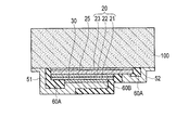
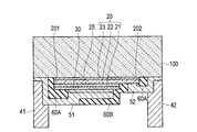
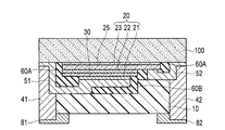
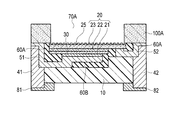
- FIG. 1 is a cross-sectional view schematically showing a structure of a light emitting device according to an embodiment of the present invention. It is a top view which shows typically the structure of the light-emitting device which concerns on embodiment of this invention. It is another top view which shows typically the structure of the light-emitting device which concerns on embodiment of this invention. It is another top view which shows typically the structure of the light-emitting device based on embodiment of this invention.
- FIG. 10 is yet another plan view schematically showing the structure of the light emitting device according to the embodiment of the present invention. It is sectional drawing which shows typically the structure of the light-emitting device which concerns on the 1st modification of embodiment of this invention.
- the light emitting device has a laminated structure in which a light emitting layer 22 and a second semiconductor layer 23 are sequentially disposed above a supporting substrate 10 and a first semiconductor layer 21. And the first light emitting element 20 disposed on the support substrate 10, the buffer layer 25 disposed on the second semiconductor layer 23, and the first semiconductor layer 21.
- a second electrode 42 electrically connected to the electrode 41, the second semiconductor layer 23, and a frame 100A disposed on the periphery of the support substrate 10 so as to cover the periphery of the light emitting element 20; And a light transmitting substrate (phosphor layer) 70 which is applied so as to completely embed the frame interior 70A formed by the frame 100A.
- the first electrode 41 is continuously disposed over the first side surface 101 of the support substrate 10 and the first side surface 201 of the light emitting element 20.
- the second electrode 42 is disposed continuously from the second side surface 102 of the support substrate 10 to the second side surface 202 of the light emitting element 20 so as to be separated from the first electrode 41.
- the first electrode 41 and the second electrode 42 are collectively referred to as “electrode region”.
- an electrode region for supplying a current to the light emitting element 20 is disposed on the side surface of the light emitting element 20.
- the support substrate 10 is disposed below the light emitting element 20 so as to be sandwiched between the first electrode 41 and the second electrode 42. Under the light emitting element 20, the support substrate 10 and the electrode region are provided. There is no boundary.
- the light emitting element 20 has a stacked structure including a first semiconductor layer 21 of a first conductivity type, a light emitting layer 22, and a second semiconductor layer 23 of a second conductivity type.
- the first conductivity type and the second conductivity type are opposite to each other. That is, if the first conductivity type is P-type, the second conductivity type is N-type, and if the first conductivity type is N-type, the second conductivity type is P-type.
- the case where the first conductivity type is P type and the second conductivity type is N type will be described as an example.
- the light emitting element 20 is an LED element in which the first semiconductor layer 21 is a P-type cladding layer and the second semiconductor layer 23 is an N-type cladding layer.
- a double hetero structure in which the first semiconductor layer 21, the light emitting layer 22, and the second semiconductor layer 23 are stacked is adopted for the light emitting element 20.
- Holes are supplied from the first electrode 41 to the first semiconductor layer 21, and electrons are supplied from the second electrode 42 to the second semiconductor layer 23. Then, holes are injected from the first semiconductor layer 21 into the light emitting layer 22, and electrons are injected from the second semiconductor layer 23. When the injected holes and electrons recombine in the light emitting layer 22, light is generated in the light emitting layer 22.
- the light emitting element 20 has the main surface of the second semiconductor layer 23 as a light extraction surface.
- the light emitted from the light emitting element 20 is transmitted, for example, through the buffer layer 25 and the light transmitting substrate 70 disposed above the second semiconductor layer 23, and is output as the output light L from the light emitting device.
- the buffer layer 25 is provided to improve the crystallinity by reducing the difference between the lattice constants of each other.
- the buffer layer 25 has a structure in which an AlN initial layer of the same second conductivity type as the second semiconductor layer 23 and a buffer layer are sequentially stacked on the semiconductor substrate 100 (not shown).
- the light transmitting substrate 70 is disposed in an area inside the side surfaces 201, 202, 203, 204 of the light emitting element 20. That is, in the light emitting device shown in FIG. 1, the frame 100A is disposed in the peripheral portion on the support substrate 10 so as to cover the peripheral portion of the light emitting element 20 and penetrates so that the outermost surface of the laminated structure is exposed. Equipped with The frame 100A is formed by penetrating a part of the semiconductor substrate 100 so as to expose the buffer layer 25 or the second semiconductor layer 23, and is formed in the frame interior 70A formed by the frame 100A. A light transmitting substrate 70 is embedded in contact with the buffer layer 25 or the second semiconductor layer 23.
- the depth of the frame interior 70A which is the substrate complete removal area (light extraction area), can be, for example, a depth obtained by removing at least a part of the buffer layer 25. Specifically, the frame interior 70 A completely removes the depth reaching the main surface of the buffer layer 25, the depth reaching the middle of the buffer layer 25, and the buffer layer 25, and the main surface of the second semiconductor layer 23 Of the first semiconductor layer 23 or the middle of the second semiconductor layer 23.
- the frame 100A is formed by leaving a part of the semiconductor substrate 100 used for forming the layers 21, 22 and 23 constituting the light emitting element 20 in a ring shape. And exposed to the side of the light emitting device.
- the film thickness of the frame 100A is set to about 1 ⁇ m to 10 ⁇ m, the mechanical strength of the entire package can be enhanced without losing the property of being the extremely small size.
- the frame interior 70A deeper, the contact area in the film thickness direction of the light transmitting substrate 70 can be increased, and it is not only difficult to peel off the light transmitting substrate 70, but also the semiconductor substrate for forming the frame 100A.
- the frame body 100A By using 100, it is possible to make the frame body 100A more resistant to peeling than in the case of bonding. In addition, even in the case of directly applying the resin in the frame interior 70A formed by the frame 100A in the formation of the light transmitting substrate 70, the frame 100A can prevent the resin from flowing out, etc. Colors are possible for each substrate (tip to tone adjustment).
- the electrode region is disposed so as to be exposed to the side surfaces 201 and 202 of the light emitting element 20, and the side surface of the frame 100A is also exposed. That is, the outer side surface of the first electrode 41 and the second electrode 42 and the outer side surface of the frame 100A are at the same plane level.
- the side surfaces of the light transmitting substrate 70 are inside the side surfaces 201, 202, 203 and 204 of the light emitting element 20, respectively.
- the frame 100A includes the side surfaces 201, 202, 203, 204 of the light emitting element 20 such that the frame interior 70A is on the inner side of the side surfaces 201, 202, 203, 204 of the light emitting element 20. It has a width that covers the Therefore, it is possible to suppress the entry of moisture or the like to the side surfaces 201, 202, 203, 204 of the light emitting element 20.
- the main surface of the light transmitting substrate 70 and the main surface of the frame 100A are at the same plane level.
- the light transmitting substrate 70 can be omitted depending on the material constituting the light emitting element 20. That is, even when applied to a light emitting device having a structure in which the light transmitting substrate is not disposed, peeling off of the light emitting element 20 or intrusion of moisture or the like to the side surfaces 201, 202, 203, 204 can be obtained by providing the frame 100A. It can be suppressed.
- a first lead-out electrode 51 connecting the first semiconductor layer 21 of the light emitting element 20 and the first electrode 41 is electrically connected to the lower surface of the first semiconductor layer 21.
- a reflective metal layer 30 is disposed on the lower surface of the first semiconductor layer 21, and the first lead electrode 51 is electrically connected to the first semiconductor layer 21 via the reflective metal layer 30. doing.
- the first lead-out electrode 51 extends in a direction perpendicular to the film thickness direction and is connected to the first electrode 41.
- the light emitted from the light emitting element 20 in the direction of the first semiconductor layer 21 is reflected on the surface of the reflective metal layer 30. That is, by the reflective metal layer 30, the emitted light of the light emitting element 20 traveling in the direction opposite to the light extraction surface can be reflected toward the light extraction surface. Therefore, the luminance of the output light L can be improved.
- the reflective metal layer 30 is made of a conductive material which has a high reflectance to the light emitted from the light emitting element 20 and which can make ohmic contact with the first semiconductor layer 21.
- a white-based metal film such as a silver-based alloy such as a silver-palladium alloy is preferably used as the material of the reflective metal layer 30.
- a second lead-out electrode 52 connecting the second semiconductor layer 23 of the light emitting element 20 and the second electrode 42 is electrically connected to the lower surface of the second semiconductor layer 23.
- the second semiconductor layer 23 extends in the horizontal direction to a region where the first semiconductor layer 21 and the light emitting layer 22 are not disposed in plan view (hereinafter referred to as “stretched region”. ).
- the second extraction electrode 52 is connected to the lower surface of the extension region of the second semiconductor layer 23.
- the second extraction electrode 52 extends in a direction perpendicular to the film thickness direction and is connected to the second electrode 42.
- the light emitting element 20, the electrode region, the first lead electrode 51, and the second lead electrode 52 are insulated and separated by the protective film 60 (60A, 60B) disposed so as to cover the side surface and the lower surface of the light emitting element 20.
- the protective film 60 for example, a SiO 2 film, a SiNx film, or a PIF (polyimide film) can be employed.
- the protective film 60 contributes to the suppression of the entry of moisture from the outside into the light emitting element 20 and the improvement of the mechanical strength of the light emitting device.
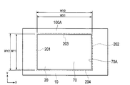
- FIG. 2 shows a plan view of the light emitting device shown in FIG. 1 along the II direction.
- the light transmitting substrate 70 has, for example, a rectangular shape, and the width in the X direction is WX1 and the width in the Y direction is WY1.
- the light emitting element 20 is rectangular, and the first side face 201 and the second side face 202 face each other, and the third side face 203 and the fourth side face 204 face each other.
- the light emitting element 20 has a width in the X direction of WX2 (WX2> WX1) and a width in the Y direction of WY2 (WY2> WY1). That is, the light transmitting substrate 70 is disposed inside the frame interior 70A formed by the frame 100A inside the side surfaces 201, 202, 203 and 204 of the light emitting element 20.
- FIG. 3 shows a plan view of the light emitting device shown in FIG. 1 along the II-II direction.
- the light emitting element 20 and the electrode region are insulated and separated by a protective film 60A.
- the support substrate 10 is formed on the third and fourth side surfaces 203 and 204 of the light emitting element 20. That is, the light emitting element 20 is disposed in the recess formed by the upper portion of the support substrate 10 and the upper portion of the electrode region.
- FIG. 4 is a plan view along the III-III direction of the light emitting device shown in FIG.
- the first extraction electrode 51 and the second extraction electrode 52 are separated by the support substrate 10 and the protective film 60B.
- FIG. 5 shows a plan view of the light emitting device shown in FIG. 1 along the IV-IV direction.
- the lower part of the light emitting device has a structure in which the first side face 101 and the second side face 102 opposite to each other of the rectangular support substrate 10 are covered by the electrode region.
- the support substrate 10 it is possible to use an epoxy resin or silicone resin containing a filler.
- a white support substrate 10 can be realized by adding a white pigment to these resins. According to the white support substrate 10, the reflectance of the support substrate 10 can be improved. As a result, the luminance of the light emitting device is improved.
- a material having a mechanical strength higher than that of a resin may be used for the support substrate 10.
- a ceramic substrate is used as the support substrate 10.
- the light transmitting substrate 70 functions as a sealing material of the light emitting element 20 and a lens of the light emitting device.
- a thermoplastic resin or a thermosetting resin can be used for the light transmitting substrate 70.
- the output light L having the same color as the light emitted from the light emitting element 20 can be output from the light emitting device.
- a phosphor resin containing a phosphor that is excited by the light emitted from the light emitting element 20 to emit excitation light may be employed as the light transmitting substrate 70.
- the output light L of a desired color can be output from the light emitting device.
- YAG yttrium aluminum garnet
- part of the blue light emitted from the light emitting element 20 is wavelength-converted to yellow light by exciting the phosphor.
- a white output light L is output from the light emitting device. Even when the output light L of the light emitting device is other than white light, various combinations of the emitted light of the light emitting element 20 and the phosphor can be adopted.
- the transparent resin used for the light transmitting substrate 70 an epoxy resin, a modified epoxy resin, a silicone resin, a modified silicone resin or the like can be adopted.
- silicone resins having high heat resistance are used.
- the phosphor resin a mixture of the above-mentioned transparent resin and the phosphor can be used.
- the CSP has a structure in which light is extracted from the direction in which the electrode region connected to the light emitting element 20 is not disposed. For this reason, since there is nothing to shield (shield) the light from the light emitting element 20 in the direction of the light extraction surface, the light emission efficiency of the light emitting device is improved. In addition, since wire bonding is not used for the electrical wiring of the electrodes, it is possible to suppress defects such as wire breakage and short circuit via the wire. Therefore, the reliability of the light emitting device is improved.
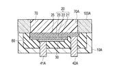
- FIG. 6 is a schematic view of a light emitting device according to a first modification of the embodiment of the present invention to which a CSP is applied.
- the supporting substrate 10A is provided so as to cover the peripheral portion of the light emitting element 20 and the light emitting element 20 disposed in the concave portion of the supporting substrate 10A provided with the concave portion in the upper portion. It comprises a frame 100A disposed in the upper peripheral portion, and a light transmitting substrate 70 disposed in the frame interior 70A of the frame 100A. That is, the lower surface and the side surface of the light emitting element 20 are surrounded by the support substrate 10A.
- the first electrode 41A penetrates the lower portion of the support substrate 10A, and is connected to the first semiconductor layer 21 via the reflective metal layer 30 in the recess of the support substrate 10A.
- the second electrode 42A penetrates the lower portion of the support substrate 10A at a position separated from the position where the first electrode 41A penetrates the support substrate 10A, and the second semiconductor layer 23 is formed in the recess of the support substrate 10A.
- Connected with the stretching area of A buffer layer 25 is provided on the light extraction surface side of the light emitting element 20 in contact with the second semiconductor layer 23.
- the light transmitting substrate 70 can be omitted depending on the material constituting the light emitting element 20.
- a protective film 60 is disposed in the remaining area inside the recess of the support substrate 10A.
- the light emitting element 20 is supported from below by the support substrate 10A, the first electrode 41A and the second electrode 42A. Therefore, due to the difference in linear expansion coefficient between the support substrate 10A and the first electrode 41A and the second electrode 42A, warpage or distortion occurs to the light emitting element 20 compared to the light emitting device shown in FIG. Cheap. That is, as the light emitting device shown in FIG. 6 has a boundary between the support substrate 10A and the electrode region below the light emitting element 20, warpage or distortion is likely to occur in the light emitting element 20.
- the frame 100A can increase the mechanical strength of the entire package, it is possible to suppress warpage and peeling of the light emitting element 20 even in the case of the light emitting device having the configuration according to the first modification.
- the effect of suppressing warpage and separation applied to the light emitting element 20 is more remarkable in the light emitting device according to the first modification.
- the peripheral portion on the support substrates 10 and 10A is provided with the frame 100A disposed so as to cover the peripheral portion of the light emitting element 20.
- the frame body 100A is a ring-shaped portion of the semiconductor substrate 100 used to form the layers 21, 22 and 23 constituting the light emitting element 20, and the mechanical strength of the entire package is enhanced. Is possible. For this reason, it is possible to suppress application of stress due to warpage or peeling to the light emitting element 20. Therefore, when the light emitting device is incorporated into, for example, a mounting substrate (product substrate), it is possible to prevent damage to the light emitting device such as breakage of the light emitting element 20 due to warpage or peeling.
- the decrease in the performance of the light emitting device and the decrease in the product life can be suppressed.
- the light emitting device according to the present invention it is possible to provide a light emitting device that can apply CSP and can suppress warpage or peeling of the light emitting element 20.
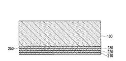
- each layer constituting the light emitting element 20 is formed on the semiconductor substrate 100 having a thickness of about 700 ⁇ m by an epitaxial growth method or the like with the buffer layer 25 interposed therebetween.
- an N-type buffer layer 250 is formed on a semiconductor substrate 100 in a wafer state
- an N-type semiconductor film 230, a light emitting region film 220, and a P-type semiconductor film 210 are sequentially stacked thereon.
- a Si substrate is used for the semiconductor substrate 100
- a nitride-based compound semiconductor layer such as gallium nitride (GaN) is used for the N-type semiconductor film 230, the light emitting region film 220, and the P-type semiconductor film 210.
- GaN gallium nitride
- the N-type buffer layer 250, the N-type semiconductor film 230, the light emitting region film 220 and the P-type semiconductor film 210 are patterned by dry etching to form the buffer layer 25, the second semiconductor layer 23, the light emitting layer 22 and the The first semiconductor layer 21 is formed.
- part of the first semiconductor layer 21 and the light emitting layer 22 is removed by dry etching or the like to expose part of the second semiconductor layer 23.
- the exposed portion is an extension area to which the second lead electrode 52 is connected.
- a protective film 60A is formed so as to cover the exposed extension regions of the first semiconductor layer 21 and the second semiconductor layer 23.
- an opening of the protective film 60A is formed on the first semiconductor layer 21, and a reflective metal layer 30 is formed to be connected to the first semiconductor layer 21 at this opening. .
- the first lead electrode 51 is formed so as to be connected to the reflective metal layer 30.
- the opening of the protective film 60A is formed on the extension region of the second semiconductor layer 23, and the second extraction electrode 52 is formed to be connected to the second semiconductor layer 23 at this opening.
- membrane etc. are used for the 1st extraction electrode 51 and the 2nd extraction electrode 52, it is preferable to use the material which reflects the emitted light from the light emitting element 20.
- an aluminum (Al) film or a silver (Ag) film is also used.
- the first electrode 41 is formed to be electrically connected to the lead-out electrode 51 of FIG.
- the second electrode 42 is formed on the second side 202 side of the light emitting element 20 so as to be electrically connected to the second lead electrode 52.
- the first electrode 41 and the second electrode 42 are formed by, for example, copper (Cu) plating.
- the material of the electrode region is selected in consideration of the overall strength of the light emitting device and the like. Besides Cu plating, an Al material or the like may be used for the electrode region.
- the protective film 60, the first extraction electrode 51, and the second extraction electrode 52 are covered so as to bury the first electrode 41 and the second electrode 42, and A support substrate 10 which does not transmit light is formed.
- a transfer mold (TRM) method or the like can be employed to form the support substrate 10.
- the surface of the support substrate 10 is etched in the film thickness direction by a back grinding process until the thickness of the support substrate 10 reaches a predetermined value.
- the lower surfaces of the first electrode 41 and the second electrode 42 are exposed below the lower surface of the support substrate 10.
- connection electrode 81 is formed to cover the lower surface of the first electrode 41
- second connection electrode 82 is formed to cover the lower surface of the second electrode 42.
- the first connection electrode 81 and the second connection electrode 82 (hereinafter collectively referred to as “connection electrodes”) are disposed on the mounting substrate when the light emitting device is attached to the mounting substrate such as a printed substrate, for example. It is used to connect the formed wiring pattern and the electrode area of the light emitting device. Solder electrodes or the like are suitably used as the connection electrodes 81 and 82.
- the support substrate may be formed to cover the lower surfaces of the support substrate 10 and the connection electrodes 81 and 82 in order to temporarily reinforce the strength of the base.
- a Si substrate or ceramic substrate having a thickness of about 1 mm is adhered to a base as a support substrate.
- the main surface side of the semiconductor substrate 100 is partially removed.
- planarization is performed by a CMP (chemical mechanical polishing) method or the like so that the film thickness in the vertical direction of the semiconductor substrate 100 becomes about 1 ⁇ m to 10 ⁇ m.
- the semiconductor substrate 100 on the main surface of the light emitting element 20 is selectively removed by dry etching using, for example, a fluorine-based gas, and the buffer layer 25 or the second semiconductor layer 23 is removed.
- the through-hole which becomes the inside 70A of a frame is formed in the depth of the extent which exposes. That is, the semiconductor substrate 100 remains in a ring shape only in the peripheral portion on the support substrate 10 by forming the frame interior 70A which is penetrated so that the outermost layer of the lower layer laminated structure is exposed in the semiconductor substrate 100. Forming a frame 100A. For example, in FIG.
- the frame 100A has a width from the side of the base of about 10 .mu.m to 100 .mu.m in consideration of the cut width at the time of dicing described later.
- the inner side is formed to cover the peripheral portion of the light emitting element 20.
- the depth of the frame interior 70A for example, as shown in FIG. 12, it is sufficient if the depth at least the buffer layer 25 on the second semiconductor layer 23 is exposed.
- the buffer layer 25 is not required or as shown in FIG. 13, when the buffer layer 25 is completely removed and the second semiconductor layer 23 is exposed, as shown in FIG. Since the buffer layer 25 is not present, the light extraction efficiency can be further improved. Further, since the contact area in the film thickness direction of the light transmitting substrate 70 becomes larger as the inside of the frame body 70B becomes deeper, it is effective for preventing the light transmitting substrate 70 from peeling off.
- the mesa angle of the bottom surface of the frame interiors 70A and 70B after etching can be set to about 70 ° to about 90 °.
- a mesa angle of about 54 ° is generated on the bottom of the frame interior 70A, 70B, the area for shielding the light increases and the light to be extracted decreases.
- the exit light extraction surface bottom of the frame interior 70A, 70B in the exposed surface of the light emitting element 20
- the area of the can be as large as possible.
- a mesa angle of about 54 ° may be generated at the bottom of the frame interior 70A, 70B.
- the wall surfaces of the frame interiors 70A and 70B are tapered, the formability of the light transmitting substrate 70 into the frame interiors 70A and 70B is improved.
- an uneven structure may be formed on the main surface of the buffer layer 25 or the second semiconductor layer 23 exposed by removing the semiconductor substrate 100.
- the uneven structure is formed by, for example, dry etching using a pattern formed by a photomask or nanoimprint.
- the light transmitting substrate 70 is formed in the frame interior 70A on the second semiconductor layer 23.
- the light transmissive substrate 70 may be omitted depending on the light emitting element 20 or the light emitting device.
- a singulation process is performed to individually separate the light emitting devices along the dicing lines DL.
- a support substrate not shown
- it is removed here.
- the light emitting device shown in FIG. 1 is completed.
- the frame 100A is formed on the peripheral portion of the support substrate 10 (10A) so as to cover the peripheral portion of the light emitting element 20. Be done.
- the frame body 100A is a ring-shaped portion of the semiconductor substrate 100 used to form the layers 21, 22 and 23 constituting the light emitting element 20, and the mechanical strength of the entire package can be enhanced. . Therefore, application of stress due to warpage or distortion to the light emitting element 20 can be suppressed. Therefore, when the light emitting device is incorporated into, for example, a mounting substrate, it is possible to prevent damage to the light emitting device such as peeling of the light emitting element 20 and destruction of the light emitting element 20.
- the supporting substrate 10 is formed by applying a resin or the like to the wafer (semiconductor substrate) on which the light emitting element 20 is formed.
- the wafer semiconductor substrate
- the light emitting device can be manufactured at low cost.
- it is also generally called a wafer level package (WLP). That is, the support substrate 10 is formed to be in direct contact with the light emitting element 20 or in direct contact with the protective film 60 and the electrode region formed on the light emitting element 20. This is the structure of the WLP. Feature. Since the package is in contact with the light emitting element 20, the mechanical strength of the light emitting element 20 can be reinforced to realize a highly reliable light emitting device.
- the frame 100A to be a reinforcing member is formed by utilizing a part of the semiconductor substrate 100. For this reason, there is no need for bonding of the reinforcing members, and the reinforcing members are not easily peeled off.
- the support substrate 10 is a resin
- a ceramic substrate for the support substrate 10 is effective in enhancing the mechanical strength of the light emitting device.
- the liquid ceramic material is formed into a predetermined shape and then sintered at a high temperature.
- the mechanical strength of the light emitting device is improved. Furthermore, since the ceramic substrate is arranged to support substantially the entire lower surface of the light emitting element 20, breakage of the light emitting element 20 due to warpage or distortion at the time of manufacturing the frame 100A can be suppressed. . In addition, it is possible to prevent the light emitting element 20 from being damaged by an impact applied to the light emitting device at the time of product assembly or handling. As described above, by using the support substrate 10 as a ceramic substrate, damage to the light emitting device and a decrease in reliability can be suppressed. In addition, damage due to thermal distortion generated by solder heat treatment or the like at the time of product assembly can be suppressed.
- the support substrate 10 is formed such that the lower surface of the first electrode 41 and the lower surface of the second electrode 42 are located below the lower surface of the support substrate 10.
- the step between the lower surface of the support substrate 10 and the lower surface of the electrode region is set to about 10 ⁇ m. This eliminates the need for polishing the ceramic substrate after forming the ceramic substrate as the support substrate 10. Therefore, damage to the supporting substrate 10 and the light emitting element 20 by the polishing process can be reduced. As a result, it is possible to suppress the decrease in the yield of the light emitting device and the decrease in the reliability.
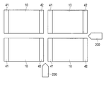
- the electrode area is formed on the side surface of the light emitting element 20, the area to be cut by the dicing blade 200 as shown in FIG. 16 and FIG. In this case, the electrode area is mainly cut more than the support substrate 10. For this reason, when the support substrate 10 is a material harder than the electrode region, such as when using a ceramic substrate, the processing time for dicing is reduced. In addition, since the life of the dicing blade is extended, the manufacturing cost can be reduced.
- the stress applied to the light emitting element 20 largely affects the characteristics of the light emitting device.
- the light emitting device to which CSP is applied has a structure in which the light emitting element 20 is in close contact with the package material, stress is easily applied to the light emitting element 20 due to the difference in linear expansion coefficient with the package material
- the first ceramic layer 11 and the second ceramic layer 12 having a higher linear expansion coefficient and a higher density than the first ceramic layer 11 are laminated on the supporting substrate 10.
- a ceramic substrate having a structure may be used.
- the light emitting element 20 is disposed on the first ceramic layer 11 having a small linear expansion coefficient.
- the second ceramic layer 12 having a large linear expansion coefficient on the side far from the light emitting element 20 of the support substrate 10, the warpage of the support substrate 10 is suppressed and the strength of the package as a whole is prevented from decreasing. it can. Therefore, by using the support substrate 10 having the structure shown in FIG. 18, a highly reliable light emitting device with high efficiency can be realized.
- there is a method of increasing the porosity In order to lower the linear expansion coefficient and the elastic coefficient of the first ceramic layer 11, for example, there is a method of increasing the porosity.
- the glass substrate when a glass substrate is used as the light transmitting substrate 70, the glass substrate has a high elastic coefficient and a large linear expansion coefficient, so that a large stress is generated in the light emitting element 20.
- the linear expansion coefficient of the first ceramic layer 11 by making the linear expansion coefficient of the first ceramic layer 11 smaller than the linear expansion coefficient of the second ceramic layer 12, the linear expansion coefficient of the first ceramic layer 11 can be made closer to glass. The stress applied to the light emitting element 20 can be reduced.
- the mechanical strength of the entire package can be increased by arranging the frame 100A on the peripheral portion of the support substrate 10 so as to cover the peripheral portion of the light emitting element 20.
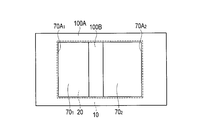
- FIG. 19 is a view schematically showing a cross-sectional structure of a light emitting device according to a third modification of the embodiment of the present invention, and FIG. 20 schematically shows a plan configuration of the light emitting device shown in FIG.
- a light-emitting device provided with a frame 100A may be configured to have a plurality of frame inside 70A 1, 70A 2. That is, in addition to the frame 100A, a partitioning frame 100B in which a part of the semiconductor substrate 100 is left is formed such that the frame interiors 70A 1 and 70A 2 are formed on the main surface of the light emitting element 20. Do. The formation of the frame 100B further improves the mechanical strength of the entire package.
- the semiconductor substrate 100 made of Si is used to form the frame body 100B, that portion becomes a shielding region. Therefore, by adjusting the size (width) of the frame body 100B and the position to be formed, the luminous intensity and color of the light emitting device can be adjusted without mixing the light transmitting substrate and adjusting the transmittance and the like. The degree can be easily suppressed.
- the frame 100 B makes it possible to form different types of light transmissive substrates 70 1 , 70 2 in the frame interior 70 A 1 , 70 A 2 . Therefore, it is possible to easily adjust the light intensity, the color tone, and the like of the light emitting element 20 while preventing the different types of light transmitting substrates 70 1 and 70 2 from being mixed by the frame 100 B.
- the partitioning frame 100B is not limited to the case where it is formed in parallel with the short direction of the base, but may be formed in parallel with the longitudinal direction of the base, for example. It may be formed in the direction. Further, the present invention is not limited to the case of providing one partitioning frame 100B, but it is also possible to dispose a plurality of frames 100B, and more interiors of the frames may be disposed. Furthermore, the inside of the frame is not limited to the rectangular shape, and for example, the planar shape may be a circle, an ellipse, or a polygon other than a rectangle.
- each of the inner angles is a polygon of 90 ° or more
- the formability of the light transmitting substrate for each corner portion can be made favorable, and the light transmitting substrate is formed inside the frame. It is possible to improve the problem of not being applied.
- the outer edge portion (peripheral portion) of the lower surface of the light emitting element 20 may partially overlap the electrode region. That is, the outer edge portion of the light emitting element 20 may overlap with the electrode region in plan view in a range in which the light emitting element 20 is not stressed so as to cause breakage or deterioration of performance.
- the semiconductor substrate 100 is a Si substrate
- a transparent substrate such as a sapphire substrate or a SiC substrate
- the frame 100A shields light, but when the semiconductor substrate 100 is a transparent substrate, a shielding layer that does not transmit light is required to the main surface of the frame 100A or the like.
- a laser lift off method or the like is used to form the frame interiors 70A and 70B.
- the formation of the buffer layer 25 can be omitted.
- the light emitting device according to the embodiment of the present invention can be used for applications of various light emitting devices to which CSP is applied.
Landscapes
- Led Device Packages (AREA)
- Led Devices (AREA)
Abstract
La présente invention comprend : un substrat de support 10 ; un élément électroluminescent 20 qui est disposé sur le substrat de support 10 et qui comprend une structure stratifiée contenant une seconde couche semi-conductrice 23 au-dessus d'une première couche semi-conductrice 21 avec une couche électroluminescente 22 entre celles-ci ; et un cadre 100A qui est disposé au niveau d'une zone périphérique au-dessus du substrat de support 10 de façon à recouvrir la périphérie de l'élément électroluminescent 20, et qui est pénétré de manière que la surface la plus haute de la structure stratifiée est exposée.
Priority Applications (2)
| Application Number | Priority Date | Filing Date | Title |
|---|---|---|---|
| PCT/JP2017/023043 WO2018235231A1 (fr) | 2017-06-22 | 2017-06-22 | Dispositif électroluminescent |
| JP2017559892A JP6536859B2 (ja) | 2017-06-22 | 2017-06-22 | 発光装置 |
Applications Claiming Priority (1)
| Application Number | Priority Date | Filing Date | Title |
|---|---|---|---|
| PCT/JP2017/023043 WO2018235231A1 (fr) | 2017-06-22 | 2017-06-22 | Dispositif électroluminescent |
Publications (1)
| Publication Number | Publication Date |
|---|---|
| WO2018235231A1 true WO2018235231A1 (fr) | 2018-12-27 |
Family
ID=64736939
Family Applications (1)
| Application Number | Title | Priority Date | Filing Date |
|---|---|---|---|
| PCT/JP2017/023043 Ceased WO2018235231A1 (fr) | 2017-06-22 | 2017-06-22 | Dispositif électroluminescent |
Country Status (2)
| Country | Link |
|---|---|
| JP (1) | JP6536859B2 (fr) |
| WO (1) | WO2018235231A1 (fr) |
Cited By (4)
| Publication number | Priority date | Publication date | Assignee | Title |
|---|---|---|---|---|
| WO2020153191A1 (fr) * | 2019-01-25 | 2020-07-30 | ソニー株式会社 | Dispositif électroluminescent et dispositif d'affichage d'image |
| JP2021072334A (ja) * | 2019-10-30 | 2021-05-06 | 日亜化学工業株式会社 | 発光装置の製造方法及び発光装置 |
| JPWO2021166785A1 (fr) * | 2020-02-19 | 2021-08-26 | ||
| US11777051B2 (en) | 2020-06-30 | 2023-10-03 | Nichia Corporation | Method of manufacturing light-emitting element |
Citations (12)
| Publication number | Priority date | Publication date | Assignee | Title |
|---|---|---|---|---|
| JP2002353507A (ja) * | 2001-05-23 | 2002-12-06 | Citizen Electronics Co Ltd | 発光ダイオードおよびその製造方法 |
| JP2003332618A (ja) * | 2002-05-10 | 2003-11-21 | Mitsubishi Cable Ind Ltd | 半導体発光素子 |
| JP2004096113A (ja) * | 2002-09-02 | 2004-03-25 | Samsung Electro Mech Co Ltd | 発光ダイオード及びその製造方法 |
| WO2006001297A1 (fr) * | 2004-06-23 | 2006-01-05 | Rohm Co., Ltd. | Dispositif émetteur de lumière blanche et sa méthode de production |
| JP2007235122A (ja) * | 2006-02-02 | 2007-09-13 | Matsushita Electric Ind Co Ltd | 半導体発光装置及びその製造方法 |
| JP2010087292A (ja) * | 2008-09-30 | 2010-04-15 | Toyoda Gosei Co Ltd | 発光素子 |
| JP2011258665A (ja) * | 2010-06-07 | 2011-12-22 | Toshiba Corp | 半導体発光装置および半導体発光装置の製造方法 |
| JP2012243849A (ja) * | 2011-05-17 | 2012-12-10 | Toshiba Corp | 半導体発光装置 |
| JP2013197309A (ja) * | 2012-03-19 | 2013-09-30 | Toshiba Corp | 発光装置 |
| JP2015111636A (ja) * | 2013-12-06 | 2015-06-18 | 日亜化学工業株式会社 | 発光装置及び発光装置の製造方法 |
| JP2016001750A (ja) * | 2015-08-19 | 2016-01-07 | 株式会社東芝 | 半導体発光装置 |
| US20160372642A1 (en) * | 2015-06-19 | 2016-12-22 | Samsung Electronics Co., Ltd. | Light emitting diode package and method of manufacturing the same |
-
2017
- 2017-06-22 WO PCT/JP2017/023043 patent/WO2018235231A1/fr not_active Ceased
- 2017-06-22 JP JP2017559892A patent/JP6536859B2/ja active Active
Patent Citations (12)
| Publication number | Priority date | Publication date | Assignee | Title |
|---|---|---|---|---|
| JP2002353507A (ja) * | 2001-05-23 | 2002-12-06 | Citizen Electronics Co Ltd | 発光ダイオードおよびその製造方法 |
| JP2003332618A (ja) * | 2002-05-10 | 2003-11-21 | Mitsubishi Cable Ind Ltd | 半導体発光素子 |
| JP2004096113A (ja) * | 2002-09-02 | 2004-03-25 | Samsung Electro Mech Co Ltd | 発光ダイオード及びその製造方法 |
| WO2006001297A1 (fr) * | 2004-06-23 | 2006-01-05 | Rohm Co., Ltd. | Dispositif émetteur de lumière blanche et sa méthode de production |
| JP2007235122A (ja) * | 2006-02-02 | 2007-09-13 | Matsushita Electric Ind Co Ltd | 半導体発光装置及びその製造方法 |
| JP2010087292A (ja) * | 2008-09-30 | 2010-04-15 | Toyoda Gosei Co Ltd | 発光素子 |
| JP2011258665A (ja) * | 2010-06-07 | 2011-12-22 | Toshiba Corp | 半導体発光装置および半導体発光装置の製造方法 |
| JP2012243849A (ja) * | 2011-05-17 | 2012-12-10 | Toshiba Corp | 半導体発光装置 |
| JP2013197309A (ja) * | 2012-03-19 | 2013-09-30 | Toshiba Corp | 発光装置 |
| JP2015111636A (ja) * | 2013-12-06 | 2015-06-18 | 日亜化学工業株式会社 | 発光装置及び発光装置の製造方法 |
| US20160372642A1 (en) * | 2015-06-19 | 2016-12-22 | Samsung Electronics Co., Ltd. | Light emitting diode package and method of manufacturing the same |
| JP2016001750A (ja) * | 2015-08-19 | 2016-01-07 | 株式会社東芝 | 半導体発光装置 |
Cited By (11)
| Publication number | Priority date | Publication date | Assignee | Title |
|---|---|---|---|---|
| WO2020153191A1 (fr) * | 2019-01-25 | 2020-07-30 | ソニー株式会社 | Dispositif électroluminescent et dispositif d'affichage d'image |
| JPWO2020153191A1 (ja) * | 2019-01-25 | 2021-12-02 | ソニーグループ株式会社 | 発光デバイスおよび画像表示装置 |
| JP7484727B2 (ja) | 2019-01-25 | 2024-05-16 | ソニーグループ株式会社 | 発光デバイスおよび画像表示装置 |
| US12068441B2 (en) | 2019-01-25 | 2024-08-20 | Sony Group Corporation | Light-emitting device and image display apparatus |
| JP2021072334A (ja) * | 2019-10-30 | 2021-05-06 | 日亜化学工業株式会社 | 発光装置の製造方法及び発光装置 |
| JP7462144B2 (ja) | 2019-10-30 | 2024-04-05 | 日亜化学工業株式会社 | 発光装置の製造方法及び発光装置 |
| US12125939B2 (en) | 2019-10-30 | 2024-10-22 | Nichia Corporation | Method of manufacturing light-emitting device and light-emitting device |
| JPWO2021166785A1 (fr) * | 2020-02-19 | 2021-08-26 | ||
| WO2021166785A1 (fr) * | 2020-02-19 | 2021-08-26 | ソニーグループ株式会社 | Élément électroluminescent, réseau d'éléments électroluminescents et dispositif d'affichage |
| JP7622730B2 (ja) | 2020-02-19 | 2025-01-28 | ソニーグループ株式会社 | 発光素子、発光素子アレイ及び表示装置 |
| US11777051B2 (en) | 2020-06-30 | 2023-10-03 | Nichia Corporation | Method of manufacturing light-emitting element |
Also Published As
| Publication number | Publication date |
|---|---|
| JP6536859B2 (ja) | 2019-07-03 |
| JPWO2018235231A1 (ja) | 2019-06-27 |
Similar Documents
| Publication | Publication Date | Title |
|---|---|---|
| TWI595686B (zh) | Semiconductor light-emitting device | |
| US10043955B2 (en) | Light emitting diode chip having wavelength converting layer and method of fabricating the same, and package having the light emitting diode chip and method of fabricating the same | |
| KR101304090B1 (ko) | 반도체 발광 장치 및 그 제조 방법 | |
| JP6106120B2 (ja) | 半導体発光装置 | |
| KR101530142B1 (ko) | 반도체 발광 장치 및 그 제조 방법 | |
| KR101158242B1 (ko) | 반도체 발광 장치 및 그 제조 방법 | |
| TWI543399B (zh) | 半導體發光裝置 | |
| JP2015195332A (ja) | 半導体発光装置及びその製造方法 | |
| CN104022216A (zh) | 发光装置 | |
| JP2015032621A (ja) | 半導体発光装置及びその製造方法 | |
| JP5837456B2 (ja) | 半導体発光装置及び発光モジュール | |
| JP6185415B2 (ja) | 半導体発光装置 | |
| JP2014150196A (ja) | 半導体発光装置およびその製造方法 | |
| JP6536859B2 (ja) | 発光装置 | |
| JP2016001750A (ja) | 半導体発光装置 | |
| JP5278175B2 (ja) | 発光装置 | |
| JP2015188039A (ja) | 半導体発光装置およびその製造方法 | |
| JP7348520B2 (ja) | 発光装置及び表示装置 | |
| JP6269901B1 (ja) | 発光装置 | |
| JP6414334B1 (ja) | 発光装置 | |
| JP6265306B1 (ja) | 発光装置 |
Legal Events
| Date | Code | Title | Description |
|---|---|---|---|
| ENP | Entry into the national phase |
Ref document number: 2017559892 Country of ref document: JP Kind code of ref document: A |
|
| 121 | Ep: the epo has been informed by wipo that ep was designated in this application |
Ref document number: 17914777 Country of ref document: EP Kind code of ref document: A1 |
|
| NENP | Non-entry into the national phase |
Ref country code: DE |
|
| 122 | Ep: pct application non-entry in european phase |
Ref document number: 17914777 Country of ref document: EP Kind code of ref document: A1 |