WO2019012663A1 - Élément d'absorption de surtension et composant électronique - Google Patents
Élément d'absorption de surtension et composant électronique Download PDFInfo
- Publication number
- WO2019012663A1 WO2019012663A1 PCT/JP2017/025597 JP2017025597W WO2019012663A1 WO 2019012663 A1 WO2019012663 A1 WO 2019012663A1 JP 2017025597 W JP2017025597 W JP 2017025597W WO 2019012663 A1 WO2019012663 A1 WO 2019012663A1
- Authority
- WO
- WIPO (PCT)
- Prior art keywords
- thermal expansion
- varistor
- exterior member
- expansion body
- electrodes
- Prior art date
- Legal status (The legal status is an assumption and is not a legal conclusion. Google has not performed a legal analysis and makes no representation as to the accuracy of the status listed.)
- Ceased
Links
Images


Classifications
-
- H—ELECTRICITY
- H01—ELECTRIC ELEMENTS
- H01C—RESISTORS
- H01C7/00—Non-adjustable resistors formed as one or more layers or coatings; Non-adjustable resistors made from powdered conducting material or powdered semi-conducting material with or without insulating material
- H01C7/10—Non-adjustable resistors formed as one or more layers or coatings; Non-adjustable resistors made from powdered conducting material or powdered semi-conducting material with or without insulating material voltage responsive, i.e. varistors
Definitions
- the present invention relates to a surge absorbing element and electronic component having a thermal expansion body for making it open.
- the surge absorbing element has a function of supplying a surge current when a high voltage, which is a voltage having a voltage value equal to or higher than a predetermined value, is applied, and protecting a circuit in the subsequent stage.
- a surge absorbing element in general, a pair of electrodes is attached to both ends of a varistor base containing a metal oxide such as ZnO (zinc oxide), an external lead is drawn from each electrode, and all of the varistor base and all of the electrodes. And a part of the external lead is covered with the exterior member.
- the varistor substrate lowers its start-up voltage each time current flows. That is, the varistor base body has a function of absorbing a surge each time a current flows, and gradually approaches a short circuit state. For this reason, in the surge absorbing element, when an excessive surge voltage is applied to the varistor base many times and deterioration progresses, it eventually becomes a short circuit failure.
- the surge absorbing element described in Patent Document 1 electrically connects a varistor base, a pair of electrodes electrically connected to both end faces of the varistor base to sandwich the varistor base, and a pair of electrodes.
- a thermal expansion body provided between an external lead, an exterior member covering an electrode, and a pair of electrodes, and irreversibly expanding by heat generated from the varistor base to separate at least one of the pair of electrodes from the varistor base.
- the thermal expansion body irreversibly expands due to the heat generation of the varistor substrate due to the current flowing to the degraded varistor substrate, and The open state is maintained.
- Patent No. 5829779 gazette
- the present invention has been made in view of the above, and it is an object of the present invention to obtain a surge absorbing element and an electronic component in which a user can freely attach and detach a thermal expansion body for bringing it into an open state. .
- a surge absorber comprises a varistor substrate.
- the surge absorbing element includes a pair of electrodes electrically connected to both end surfaces of the varistor base to hold the varistor base.
- the surge absorbing element includes an external lead electrically connected to each of the pair of electrodes.
- the surge absorbing element covers the varistor base and the pair of electrodes, and includes an exterior member having a depression located between the pair of electrodes on the surface.
- the surge absorbing element is disposed in the recess, and includes a thermal expansion body which irreversibly expands due to the heat generated from the varistor base to separate at least one of the pair of electrodes from the varistor base.
- the surge absorbing element according to the present invention has an effect that the user can freely attach and detach the thermal expansion body for making the open (opened) state.
- Sectional view of a surge absorber according to a first embodiment of the present invention Sectional view of a surge absorber according to a first embodiment of the present invention Sectional drawing of the open (opened) state of the surge absorption element concerning Embodiment 1 of the present invention
- the perspective view for demonstrating the electronic component concerning Embodiment 2 of this invention The perspective view for demonstrating the electronic component concerning Embodiment 2 of this invention
- FIG. 1 and 2 are cross-sectional views of a surge absorber according to a first embodiment of the present invention.
- FIG. 3 is a cross-sectional view of an open (opened) state of the surge absorber according to the first embodiment of the present invention.
- the surge absorbing element 10 has a function of flowing a surge current when a high voltage which is a voltage of a voltage value equal to or higher than a predetermined value is applied, ie, a function of absorbing a surge.
- the surge absorber 10 shown in FIG. 1 includes a varistor base 11, a pair of electrodes 12a and 12b, external leads 13a and 13b, and an exterior member 14.
- the surge absorber 10 shown in FIGS. 2 and 3 further includes a thermal expansion body 16.
- the varistor substrate 11 contains, for example, a metal oxide such as ZnO (zinc oxide) or SrTiO 3 (strontium titanate), but the material that can be used for the varistor substrate 11 is limited to the above-mentioned metal oxides. is not.
- the varistor substrate 11 has a pair of end surfaces 11Ta and 11Tb and side portions 11S. The side portion 11S connects the pair of end surfaces 11Ta and 11Tb.
- the pair of electrodes 12a and 12b are electrically connected to both end faces 11Ta and 11Tb of the varistor base body 11, respectively. Specifically, electrode 12 a is electrically connected to end surface 11 Ta of varistor base 11, and electrode 12 b is electrically connected to end surface 11 Tb of varistor base 11. The pair of electrodes 12a and 12b are not electrically connected. With such a structure, the varistor base 11 is sandwiched between the pair of electrodes 12a and 12b.
- the external leads 13a and 13b are electrically connected to the pair of electrodes 12a and 12b, respectively.
- the exterior member 14 covers the varistor base 11 and the pair of electrodes 12a and 12b.
- the exterior member 14 has a recess 15 on the surface and between the pair of electrodes 12a and 12b.
- the recess 15 is formed in the exterior member 14 along the periphery of the varistor base 11.
- an angle formed by the upper surface 14a which is the upper surface of the exterior member 14 and the side surface 14b of the exterior member 14 which is the side surface of the recess 15 formed in the exterior member 14 be 90 °.
- the both sides 14b and 14c of the exterior member 14 used as the both sides of the hollow 15 formed in the exterior member 14 are parallel.
- the recess 15 is located between the pair of electrodes 12a and 12b. That is, the bottom surface 14d of the exterior member 14, which is the bottom surface of the recess 15 formed in the exterior member 14, is located between the pair of electrodes 12a and 12b.
- the varistor substrate 11 and the electrode 12b are bonded by, for example, a conductive adhesive and electrically connected.
- the varistor base 11 and the electrode 12a are, for example, separable and electrically connected by a conductive paste or the like having weaker adhesion than a conductive adhesive.
- at least one of the varistor base 11 and the electrode 12b, and the varistor base 11 and the electrode 12a may be separable and electrically connected. Therefore, both of the varistor base 11 and the electrode 12b and the varistor base 11 and the electrode 12a may be electrically connected by, for example, a conductive paste.
- the thermal expansion body 16 is arrange
- the thermal expansion body 16 may be fitted into the recess 15 of the exterior member 14.
- the thickness of the thermal expansion body 16 be larger than the size between the side surfaces 14b and 14c.
- the thickness of the thermal expansion body 16 refers to the dimension in the direction from the side surface 14 b to 14 c in the thermal expansion body 16 before the thermal expansion body 16 is fitted into the recess 15.
- the thermal expansion body 16 may be attached to the recess 15 of the exterior member 14 using an adhesive or the like.
- the thermal expansion body 16 irreversibly expands due to the heat generated from the varistor base 11 and separates at least one of the pair of electrodes 12 a and 12 b from the varistor base 11.
- the thermal expansion body 16 expands to make the electrode 12a a varistor base. It is pulled away from 11.
- the electrode 12 b may be separated from the varistor substrate 11, or both of the electrodes 12 a and 12 b may be separated from the varistor substrate 11.
- the thermal expansion body 16 is, for example, a resin irreversibly expandable by heat.
- a resin irreversibly expandable by heat for example, a resin of model number AF-3024 manufactured by 3M (registered trademark) Japan Ltd. is used.
- 3M registered trademark
- the thermal expansion body 16 does not decrease in volume even after cooling once a plurality of pores are formed inside.
- the thermal expansion body 16 expands irreversibly. That is, the thermal expansion body 16 maintains the expanded state once expanded.
- the thermal expansion body 16 irreversibly expands to increase the size of the outer shape, the distance between the electrode 12a and the electrode 12b increases. As a result, as shown in FIG. 3, the thermal expansion body 16 separates the electrode 12 a from the varistor base 11 to form an insulating gap 17 between the varistor base 11 and the electrode 12 a.
- the surge absorbing element 10 is in an open state, and therefore no current flows in the varistor substrate 11 even if a voltage is applied to the pair of electrodes 12 a and 12 b.
- the thermal expansion body 16 irreversibly expands due to the heat generation of the varistor base 11 due to the current flowing to the deteriorated varistor base 11. Therefore, once the thermal expansion body 16 expands, the surge absorbing element 10 maintains the state in which the insulating gap 17 is formed between the varistor base 11 and the electrode 12a, as shown in FIG. As a result, the surge absorber 10 is maintained in the open state once the thermal expansion body 16 is expanded. In the surge absorbing element 10, a current does not flow to the varistor base 11 after the thermal expansion body 16 is expanded, so that the power supply line, circuit or the surge absorbing element 10 is attached in a state where the function of absorbing surge is lowered. It is possible to suppress the occurrence of a short circuit failure of devices. Further, the temperature rise of the varistor base 11 and the exterior member 14 is suppressed in the state where the function of absorbing the surge is lowered.
- the temperature at which the thermal expansion body 16 starts irreversible expansion is referred to as an expansion start temperature.
- the thermal expansion body 16 irreversibly expands when reaching the expansion start temperature or more.
- the expansion start temperature is, for example, 180 ° C.
- the expansion start temperature is not limited to 180 ° C. as described above because it varies depending on the specification of the resin irreversibly expandable by heat.
- the expansion start temperature is, for example, preferably equal to or less than the heat resistance temperature of the exterior member 14, and more preferably about 5 ° C. to 10 ° C. lower than the heat resistance temperature of the exterior member 14.
- the thermal expansion body 16 irreversibly expands, and the open (open) state on the safety side is maintained. .
- current does not flow to the surge absorbing element 10 whose function of absorbing the surge is degraded, so that occurrence of a short circuit failure of the circuit or equipment to which the surge absorbing element 10 is attached can be suppressed.
- the surge absorbing element 10 can suppress the current from continuing to flow through the varistor base 11 in the state where the function of absorbing the surge is deteriorated.
- the safety of the surge absorbing element 10 is improved.
- the thermal expansion body 16 irreversibly expands below the heat resistance temperature of the exterior member 14, the exterior member 14 can be used below the heat resistance temperature.
- the recess 15 is formed on the surface of the exterior member 14, and the thermal expansion body 16 for bringing it into the open (opened) state is disposed in the recess 15 formed on the surface of the exterior member 14.
- the user can optionally attach and detach the thermal expansion body 16 for bringing the thermal expansion body 16 into an open state.
- An angle formed by an upper surface 14a which is the upper surface of the exterior member 14 and a side surface 14b of the exterior member 14 which is a side surface of the recess 15 formed in the exterior member 14 is 90 °
- both side surfaces 14 b and 14 c of the exterior member 14 which are both side surfaces 15 are parallel, the user can more easily attach and detach the thermal expansion body 16 to the surge absorbing element 10.
- the thermal expansion body 16 is fitted into the recess 15, the electrode 12 a is easily pulled away from the varistor base 11.
- the recess 15 is formed on the surface of the exterior member 14, and the thermal expansion body 16 for making the open (opened) state is disposed in the recess 15 formed on the surface of the exterior member 14.
- the manufacturing process of the surge absorbing element is simplified, that is, the manufacturing adding the process of forming the recess 15 after the normal manufacturing process of the surge absorbing element.
- the manufacturing cost of the surge absorber 10 can be reduced.
- the user when the user adds the function of bringing the surge absorbing element 10 into the open (open) state, for example, the user places the thermal expansion body 16 in the recess 15 formed on the surface of the exterior member 14. It should be arranged. For this reason, the surge absorber 10 can be easily handled.
- the thermally expandable body 16 is a resin which is irreversibly expanded by heat, but is not limited to the resin as long as it is irreversibly expanded by heat.
- the thermal expansion body 16 may be a shape memory alloy that deforms so as to increase the distance between the pair of electrodes 12a and 12b when the temperature reaches the expansion start temperature or more.
- the thermal expansion body 16 may be a structure such as a vaporized substance or a material having a large thermal expansion coefficient enclosed in a container made of a plastically deformable material.
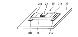
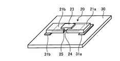
- FIG. 4 and 5 are perspective views for explaining an electronic component according to a second embodiment of the present invention.
- FIG. 6 is a perspective view for explaining the open (opened) state of the electronic component according to the second embodiment of the present invention.
- the resistor 20 which is an electronic component according to the present embodiment shown in FIG. 4 includes exterior members 21 a and 21 b which cover the resistor 25 inside the resistor 20.
- the exterior members 21a and 21b and the resistor 25 are joined using an adhesive or the like.
- the resistor 25 is present inside the exterior member 21a and inside the exterior member 21b.
- the resistor 25 is an example of an element.
- the resistor 20 shown in FIGS. 5 and 6 further includes a thermal expansion body 23.
- the resistor 20 is provided on the lands 31 a and 31 b provided on the substrate 30. 4 to 6, one end of the resistor 25 is electrically connected to the land 31a, and the other end of the resistor 25 is electrically connected to the land 31b.
- the exterior member 21a has a recess 22a on the surface and on the exterior member 21b side.
- the exterior member 21b has a recess 22b on the surface and on the exterior member 21a side.
- the recess 22a and the recess 22b form one recess 22.
- the thermal expansion body 23 is arrange
- the thermal expansion body 23 may be fitted into the recess 22 of the exterior members 21a and 21b.
- the thermal expansion body 23 may be attached to the recess 22 of the exterior members 21a and 21b using an adhesive or the like.
- the thermal expansion body 23 is expanded by the heat generated from the resistor 20 to physically separate the exterior member 21 a and the exterior member 21 b.
- the resistor 25 is separated by the force generated by the expansion of the thermal expansion body 23. When the package member 21a and the package member 21b are physically separated, the resistor 25 inside the resistor 20 is physically separated, and the resistor 25 is in an open (opened) state.
- heat is generated from the resistor 20 when a large current flows in the resistor 20 due to some abnormality.
- the heat generated in this manner is transmitted to the thermal expansion body 23, whereby the thermal expansion body 23 expands (thermal expansion) to physically separate the exterior member 21a and the exterior member 21b and to physically separate the resistor 25. Separate.
- the thermal expansion body 23 is, for example, a thermally expandable resin.
- the thermal expansion body 23 expands to increase the size of the outer shape, the exterior member 21a and the exterior member 21b are physically separated. As a result, as shown in FIG. 6, the thermal expansion body 23 forms an insulation gap 24 between the exterior member 21a and the exterior member 21b.
- the insulation gap 24 physically and electrically separates the resistor 20.
- the resistor 25 is physically separated, and the resistor 20 is in an open (opened) state, so that a voltage is applied to the electrodes of the resistor 20. Also, no current flows in the resistor 25.
- the thermal expansion body 23 expands to physically separate the exterior member 21 a and the exterior member 21 b and to separate the resistor 25. Physically separate. Thereby, the resistor 20 is in an open (open) state. That is, since the resistor 20 can have the function of a fuse, the need for separately providing a fuse can be eliminated.
- the recess 22 is formed in the exterior members 21a and 21b, and the thermal expansion body 23 for causing the open (opened) state is disposed in the recess 22 formed in the exterior members 21a and 21b.
- the user can optionally attach and detach the thermal expansion body 23 for bringing the thermal expansion body 23 into an open (open) state from the resistor 20 which is an electronic component.
- the recess 22 is formed in the exterior members 21a and 21b, and the thermal expansion body 23 for causing the open (opened) state is disposed in the recess 22 formed in the exterior members 21a and 21b.
- the manufacturing process of the resistor 20 is simplified, that is, the manufacturing process adding the process of forming the recess 22 after the normal manufacturing process of the resistor.
- the manufacturing cost of the resistor 20 which is an electronic component can be reduced.
- the resistor 20 when the user adds a function to open (open) the resistor 20, for example, the user arranges the thermal expansion body 23 in the recess 22 formed in the exterior members 21a and 21b. do it. For this reason, the resistor 20 which is an electronic component can be handled easily.
- the electronic component is the resistor 20, but the electronic component is not limited to the resistor 20.
- the present invention is applicable to any electronic component that generates heat due to the flow of a large current and needs to have a fuse function.
- the configuration shown in the above embodiment shows an example of the contents of the present invention, and can be combined with another known technique, and one of the configurations is possible within the scope of the present invention. It is also possible to omit and change parts.
Landscapes
- Engineering & Computer Science (AREA)
- Microelectronics & Electronic Packaging (AREA)
- Physics & Mathematics (AREA)
- Electromagnetism (AREA)
- Thermistors And Varistors (AREA)
Abstract
Cet élément d'absorption de surtension (10) comprend : un corps de base de varistance (11); une paire d'électrodes (12a, 12b) connectées électriquement à deux faces d'extrémité du corps de base de varistance (11) et prenant en sandwich le corps de base de varistance (11); des conducteurs externes (13a, 13b) connectés électriquement à la paire d'électrodes (12a, 12b); un élément de boîtier (14) recouvrant le corps de base de varistance (11) et la paire d'électrodes (12a, 12b) et présentant sur sa surface des évidements positionnés entre la paire d'électrodes (12a, 12b); et un corps à dilatation thermique (16) qui est disposé dans les évidements et se dilate de manière irréversible en réaction à la chaleur générée par le corps de base de varistance (11) de manière à séparer au moins une électrode de la paire d'électrodes (12a, 12b) du corps de base de varistance (11).
Priority Applications (3)
| Application Number | Priority Date | Filing Date | Title |
|---|---|---|---|
| CN201790000796.8U CN210467451U (zh) | 2017-07-13 | 2017-07-13 | 浪涌吸收元件及电子部件 |
| PCT/JP2017/025597 WO2019012663A1 (fr) | 2017-07-13 | 2017-07-13 | Élément d'absorption de surtension et composant électronique |
| JP2018510138A JP6333501B1 (ja) | 2017-07-13 | 2017-07-13 | サージ吸収素子および電子部品 |
Applications Claiming Priority (1)
| Application Number | Priority Date | Filing Date | Title |
|---|---|---|---|
| PCT/JP2017/025597 WO2019012663A1 (fr) | 2017-07-13 | 2017-07-13 | Élément d'absorption de surtension et composant électronique |
Publications (1)
| Publication Number | Publication Date |
|---|---|
| WO2019012663A1 true WO2019012663A1 (fr) | 2019-01-17 |
Family
ID=62238882
Family Applications (1)
| Application Number | Title | Priority Date | Filing Date |
|---|---|---|---|
| PCT/JP2017/025597 Ceased WO2019012663A1 (fr) | 2017-07-13 | 2017-07-13 | Élément d'absorption de surtension et composant électronique |
Country Status (3)
| Country | Link |
|---|---|
| JP (1) | JP6333501B1 (fr) |
| CN (1) | CN210467451U (fr) |
| WO (1) | WO2019012663A1 (fr) |
Citations (7)
| Publication number | Priority date | Publication date | Assignee | Title |
|---|---|---|---|---|
| US4047143A (en) * | 1976-07-09 | 1977-09-06 | Western Electric Company, Inc. | Fused resistive electrical protection device |
| JPS636701U (fr) * | 1986-07-01 | 1988-01-18 | ||
| JP2004095609A (ja) * | 2002-08-29 | 2004-03-25 | Matsushita Electric Ind Co Ltd | 外装被覆形バリスタ |
| JP2011077234A (ja) * | 2009-09-30 | 2011-04-14 | Nec Personal Products Co Ltd | 電子部品およびプリント基板 |
| WO2011054523A1 (fr) * | 2009-11-05 | 2011-05-12 | Phoenix Contact Gmbh & Co. Kg | Appareil électrique |
| US20120229246A1 (en) * | 2009-11-05 | 2012-09-13 | Phoenix Contact Gmbh & Co. Kg | Overvoltage protection element |
| JP5829779B1 (ja) * | 2014-05-23 | 2015-12-09 | 三菱電機株式会社 | サージ吸収素子 |
-
2017
- 2017-07-13 WO PCT/JP2017/025597 patent/WO2019012663A1/fr not_active Ceased
- 2017-07-13 CN CN201790000796.8U patent/CN210467451U/zh not_active Expired - Fee Related
- 2017-07-13 JP JP2018510138A patent/JP6333501B1/ja not_active Expired - Fee Related
Patent Citations (7)
| Publication number | Priority date | Publication date | Assignee | Title |
|---|---|---|---|---|
| US4047143A (en) * | 1976-07-09 | 1977-09-06 | Western Electric Company, Inc. | Fused resistive electrical protection device |
| JPS636701U (fr) * | 1986-07-01 | 1988-01-18 | ||
| JP2004095609A (ja) * | 2002-08-29 | 2004-03-25 | Matsushita Electric Ind Co Ltd | 外装被覆形バリスタ |
| JP2011077234A (ja) * | 2009-09-30 | 2011-04-14 | Nec Personal Products Co Ltd | 電子部品およびプリント基板 |
| WO2011054523A1 (fr) * | 2009-11-05 | 2011-05-12 | Phoenix Contact Gmbh & Co. Kg | Appareil électrique |
| US20120229246A1 (en) * | 2009-11-05 | 2012-09-13 | Phoenix Contact Gmbh & Co. Kg | Overvoltage protection element |
| JP5829779B1 (ja) * | 2014-05-23 | 2015-12-09 | 三菱電機株式会社 | サージ吸収素子 |
Also Published As
| Publication number | Publication date |
|---|---|
| JP6333501B1 (ja) | 2018-05-30 |
| CN210467451U (zh) | 2020-05-05 |
| JPWO2019012663A1 (ja) | 2019-07-11 |
Similar Documents
| Publication | Publication Date | Title |
|---|---|---|
| JP6360273B1 (ja) | 温度センサ、センサ素子及び温度センサの製造方法 | |
| JP6213698B2 (ja) | コイル内蔵多層基板およびその製造方法 | |
| CN104716627B (zh) | 整合式电涌吸收装置 | |
| CN101630674B (zh) | 包括电阻和熔线元件的电路保护装置 | |
| CN105849827A (zh) | 片形电阻器 | |
| US9916929B2 (en) | Electronic component | |
| TWI564915B (zh) | 電路保護裝置 | |
| US20180082784A1 (en) | Ceramic electronic component and mounting structure of the same | |
| CN111132390A (zh) | Ptc加热模块和制造所述ptc加热模块的方法 | |
| JP6333501B1 (ja) | サージ吸収素子および電子部品 | |
| JP5829779B1 (ja) | サージ吸収素子 | |
| JP2014241190A (ja) | Ptcヒータ | |
| JP6383013B2 (ja) | 電子デバイス | |
| JP6262462B2 (ja) | フィルムコンデンサ | |
| JP4403760B2 (ja) | 積層型圧電体素子及びその製造方法 | |
| JPH11176695A (ja) | 過電流・過熱保護機能付積層セラミックコンデンサ | |
| JP2011049418A (ja) | コモンモードノイズフィルタ | |
| JP7396042B2 (ja) | 電子部品装置 | |
| JP2014175129A (ja) | ヒューズ | |
| CN207082561U (zh) | 动力电池盖板及其动力电池 | |
| JP2011077234A (ja) | 電子部品およびプリント基板 | |
| JP3132751U (ja) | 突入電流制限用サーミスタ | |
| TWI612541B (zh) | 超級電容器的封裝結構 | |
| JP2014175146A (ja) | ヒューズ | |
| JP3137482U (ja) | 防爆型抵抗器 |
Legal Events
| Date | Code | Title | Description |
|---|---|---|---|
| ENP | Entry into the national phase |
Ref document number: 2018510138 Country of ref document: JP Kind code of ref document: A |
|
| 121 | Ep: the epo has been informed by wipo that ep was designated in this application |
Ref document number: 17917664 Country of ref document: EP Kind code of ref document: A1 |
|
| NENP | Non-entry into the national phase |
Ref country code: DE |
|
| 122 | Ep: pct application non-entry in european phase |
Ref document number: 17917664 Country of ref document: EP Kind code of ref document: A1 |