WO2019013084A1 - コイン形電池およびその製造方法 - Google Patents
コイン形電池およびその製造方法 Download PDFInfo
- Publication number
- WO2019013084A1 WO2019013084A1 PCT/JP2018/025486 JP2018025486W WO2019013084A1 WO 2019013084 A1 WO2019013084 A1 WO 2019013084A1 JP 2018025486 W JP2018025486 W JP 2018025486W WO 2019013084 A1 WO2019013084 A1 WO 2019013084A1
- Authority
- WO
- WIPO (PCT)
- Prior art keywords
- positive electrode
- electrode layer
- layer
- coin
- negative electrode
- Prior art date
- Legal status (The legal status is an assumption and is not a legal conclusion. Google has not performed a legal analysis and makes no representation as to the accuracy of the status listed.)
- Ceased
Links
Images


Classifications
-
- H—ELECTRICITY
- H01—ELECTRIC ELEMENTS
- H01M—PROCESSES OR MEANS, e.g. BATTERIES, FOR THE DIRECT CONVERSION OF CHEMICAL ENERGY INTO ELECTRICAL ENERGY
- H01M10/00—Secondary cells; Manufacture thereof
- H01M10/05—Accumulators with non-aqueous electrolyte
- H01M10/056—Accumulators with non-aqueous electrolyte characterised by the materials used as electrolytes, e.g. mixed inorganic/organic electrolytes
- H01M10/0561—Accumulators with non-aqueous electrolyte characterised by the materials used as electrolytes, e.g. mixed inorganic/organic electrolytes the electrolyte being constituted of inorganic materials only
- H01M10/0562—Solid materials
-
- B—PERFORMING OPERATIONS; TRANSPORTING
- B05—SPRAYING OR ATOMISING IN GENERAL; APPLYING FLUENT MATERIALS TO SURFACES, IN GENERAL
- B05D—PROCESSES FOR APPLYING FLUENT MATERIALS TO SURFACES, IN GENERAL
- B05D1/00—Processes for applying liquids or other fluent materials
- B05D1/02—Processes for applying liquids or other fluent materials performed by spraying
- B05D1/04—Processes for applying liquids or other fluent materials performed by spraying involving the use of an electrostatic field
- B05D1/06—Applying particulate materials
-
- H—ELECTRICITY
- H01—ELECTRIC ELEMENTS
- H01M—PROCESSES OR MEANS, e.g. BATTERIES, FOR THE DIRECT CONVERSION OF CHEMICAL ENERGY INTO ELECTRICAL ENERGY
- H01M10/00—Secondary cells; Manufacture thereof
- H01M10/04—Construction or manufacture in general
- H01M10/0468—Compression means for stacks of electrodes and separators
-
- H—ELECTRICITY
- H01—ELECTRIC ELEMENTS
- H01M—PROCESSES OR MEANS, e.g. BATTERIES, FOR THE DIRECT CONVERSION OF CHEMICAL ENERGY INTO ELECTRICAL ENERGY
- H01M10/00—Secondary cells; Manufacture thereof
- H01M10/05—Accumulators with non-aqueous electrolyte
- H01M10/058—Construction or manufacture
- H01M10/0585—Construction or manufacture of accumulators having only flat construction elements, i.e. flat positive electrodes, flat negative electrodes and flat separators
-
- H—ELECTRICITY
- H01—ELECTRIC ELEMENTS
- H01M—PROCESSES OR MEANS, e.g. BATTERIES, FOR THE DIRECT CONVERSION OF CHEMICAL ENERGY INTO ELECTRICAL ENERGY
- H01M50/00—Constructional details or processes of manufacture of the non-active parts of electrochemical cells other than fuel cells, e.g. hybrid cells
- H01M50/10—Primary casings; Jackets or wrappings
- H01M50/102—Primary casings; Jackets or wrappings characterised by their shape or physical structure
- H01M50/109—Primary casings; Jackets or wrappings characterised by their shape or physical structure of button or coin shape
-
- H—ELECTRICITY
- H01—ELECTRIC ELEMENTS
- H01M—PROCESSES OR MEANS, e.g. BATTERIES, FOR THE DIRECT CONVERSION OF CHEMICAL ENERGY INTO ELECTRICAL ENERGY
- H01M2300/00—Electrolytes
- H01M2300/0017—Non-aqueous electrolytes
- H01M2300/0065—Solid electrolytes
- H01M2300/0068—Solid electrolytes inorganic
-
- Y—GENERAL TAGGING OF NEW TECHNOLOGICAL DEVELOPMENTS; GENERAL TAGGING OF CROSS-SECTIONAL TECHNOLOGIES SPANNING OVER SEVERAL SECTIONS OF THE IPC; TECHNICAL SUBJECTS COVERED BY FORMER USPC CROSS-REFERENCE ART COLLECTIONS [XRACs] AND DIGESTS
- Y02—TECHNOLOGIES OR APPLICATIONS FOR MITIGATION OR ADAPTATION AGAINST CLIMATE CHANGE
- Y02E—REDUCTION OF GREENHOUSE GAS [GHG] EMISSIONS, RELATED TO ENERGY GENERATION, TRANSMISSION OR DISTRIBUTION
- Y02E60/00—Enabling technologies; Technologies with a potential or indirect contribution to GHG emissions mitigation
- Y02E60/10—Energy storage using batteries
-
- Y—GENERAL TAGGING OF NEW TECHNOLOGICAL DEVELOPMENTS; GENERAL TAGGING OF CROSS-SECTIONAL TECHNOLOGIES SPANNING OVER SEVERAL SECTIONS OF THE IPC; TECHNICAL SUBJECTS COVERED BY FORMER USPC CROSS-REFERENCE ART COLLECTIONS [XRACs] AND DIGESTS
- Y02—TECHNOLOGIES OR APPLICATIONS FOR MITIGATION OR ADAPTATION AGAINST CLIMATE CHANGE
- Y02P—CLIMATE CHANGE MITIGATION TECHNOLOGIES IN THE PRODUCTION OR PROCESSING OF GOODS
- Y02P70/00—Climate change mitigation technologies in the production process for final industrial or consumer products
- Y02P70/50—Manufacturing or production processes characterised by the final manufactured product
Definitions
- the present invention relates to a coin cell having a solid electrolyte layer.
- the all solid battery generally has a small output and has a problem that a necessary current can not be obtained because the capacity is small.
- Patent Document 3 discloses a coin-shaped battery provided with an elastic body that applies pressure to a battery element provided inside a metal case as a coin-shaped all solid battery that solves such a problem.
- the output can be increased by suppressing the decrease in current density due to the contact failure by increasing the contact surface pressure between the electrode constituting the battery element and the solid electrolyte with an elastic body.
- Japanese Patent Publication No. 2011-159413 Japanese patent publication "patent 5317195 (issued on October 16, 2013)”
- Japanese Patent Publication Japanese Unexamined Patent Publication No. 2010-56067 (released on March 11, 2010)"
- An object of the present invention is to realize weight reduction and miniaturization of a coin battery.
- a coin battery includes a first electrode layer, a second electrode layer having a polarity opposite to the polarity of the first electrode layer, and the first electrode. And at least one laminated body in which a solid electrolyte layer interposed between the layer and the second electrode layer is laminated, and an outer package enclosing the laminated body, the laminated body is compressed by pressure and
- the average thickness of the solid electrolyte layer in each laminate is 5 ⁇ m or more and 100 ⁇ m or less.
- the manufacturing method of the coin type battery concerning one mode of the present invention has the 1st electrode layer, the 2nd electrode layer which has the opposite polarity to the polarity of the 1st electrode layer, and the above-mentioned
- a method of manufacturing a coin-shaped battery comprising: manufacturing a coin-shaped battery having at least one laminate in which a first electrode layer and a solid electrolyte layer interposed between the second electrode layers are stacked, the method comprising the steps of: Forming the layer, forming the solid electrolyte layer on the first electrode layer, and forming the second electrode layer on the solid electrolyte layer to produce the laminate, and pressing the laminate.
- the solid electrolyte layer is formed by a powder film forming method using electrostatic force, including each step.
- Embodiment 1 The following description will explain Embodiment 1 of the present invention with reference to FIG. 1 and FIG.
- an all solid secondary battery using a lithium ion conductive solid electrolyte that is, an all solid lithium ion secondary battery will be described as an example of a coin battery.
- the coin-type battery according to the present invention is not limited to the all solid lithium ion secondary battery.
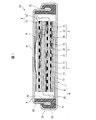
- FIG. 1 is a cross-sectional view showing the structure of the coin battery 101 according to the first embodiment.
- the coin battery 101 includes laminates 1 to 3, a positive electrode current collector group 4, a negative electrode current collector group 5, a pressure member 6, a metal case 7, and a metal.
- a sealing plate 8 and a gasket 9 are provided.
- the lower side is the positive electrode side of the coin battery 101
- the upper side is the negative electrode side of the coin battery 101.
- the laminates 1 to 3, the positive electrode current collector group 4, the negative electrode current collector group 5 and the pressing member 6 are drawn at a distance from each other for convenience, they are adjacent to each other. Contact with The later-described FIGS. 3 and 5 to 9 are also drawn similarly to FIG.
- the metal case 7 is formed of metal, and has a circular flat plate portion 71 and a side wall portion 72.
- the side wall portion 72 is formed to be bent from the outer peripheral portion of the flat plate portion 71.
- the end edge portion of the side wall portion 72 is curved toward the inside of the coin battery 101 to form a circular opening portion 73.
- the metal sealing plate 8 is formed of metal and has a circular flat plate portion 81 and a side wall portion 82.
- the flat plate portion 81 is formed smaller than the opening 73 of the metal case 7.
- the side wall portion 82 is formed to be bent from the outer peripheral portion of the flat plate portion 81.
- the edge of the side wall 82 is folded to the outer peripheral surface of the side wall 82.
- the end edges of the side wall portion 82 may not be folded.
- the sizes of the metal case 7 and the metal sealing plate 8 be appropriately selected in accordance with the use of the coin battery 101. Moreover, it is preferable that the material and the like of the metal case 7 and the metal sealing plate 8 be appropriately selected according to the temperature range in which the coin battery 101 is used.
- the gasket 9 is annularly formed of a resin having elasticity and insulating properties, and has an inner circumferential portion 91 and an outer circumferential portion 92.
- the inner circumferential portion 91 is along the inner circumferential surface of the side wall portion 82 of the metal sealing plate 8 between the inner surface of the flat plate portion 71 of the metal case 7 and the inner surface of the flat portion 81 of the metal sealing plate 8.
- the outer peripheral portion 92 is disposed so as to extend from the inner surface of the flat plate portion 71 of the metal case 7 to the outer peripheral surface of the flat plate portion 81 of the metal sealing plate 8 from the inner peripheral surface of the side wall portion 72 of the metal case 7 It is done.
- the outer peripheral portion 92 is not limited to such a structure.
- the end edge of the side wall portion 72 is curved so as to face the inside of the coin battery 101 as described above, so as to sandwich the side wall portion 82 of the metal sealing plate 8 and the outer peripheral portion 92 of the gasket 9.
- the side wall portion 82 is crimped.
- the metal case 7 (positive electrode) and the metal sealing plate 8 (negative electrode) are insulated, the metal case 7 and the metal sealing plate 8 are combined, and the metal case 7 and the metal seal are formed.
- the space between the plate 8 is sealed.
- a space sealed between the flat plate portion 71 of the metal case 7, the flat plate portion 81 of the metal sealing plate 8, and the inner circumferential portion 91 of the gasket 9 is formed.
- the laminates 1 to 3, the positive electrode current collector group 4, the negative electrode current collector group 5, and the pressure member 6 are disposed in this space.
- the pressing member 6 is a member for pressing the laminates 1 to 3, the positive electrode current collector group 4 and the negative electrode current collector group 5 which are stacked as described later.
- the pressure member 6 is constituted by a spring element such as a leaf spring, a shim or the like, and is formed of a conductive or insulating material. The pressure member 6 presses the laminates 1 to 3, the positive electrode current collector group 4 and the negative electrode current collector group 5 by their elastic force and brings them into close contact.
- the pressure member 6 is not provided for the purpose of applying a large pressure to the laminates 1 to 3, but the positive electrode current collector group 4, the negative electrode current collector group 5 and the metal case 7 or metal It is provided for the purpose of obtaining contact with the sealing plate 8 and for making constant the pressure applied to the laminates 1 to 3. Therefore, the shape of the pressure member 6 is not limited to a flat plate.
- the pressing member 6 may be a disc having a convex central portion or a hollow like a washer depending on the thickness of the laminates 1 to 3 or the deformed state of the metal case 7 after caulking or the like. It is necessary to select and use a member or even a corrugated washer.
- the laminates 1 to 3 are arranged in the order of the laminate 1, the laminate 2 and the laminate 3 from the positive electrode side.
- a positive electrode layer 11 (first electrode layer), a solid electrolyte layer 12, and a negative electrode layer 13 (second electrode layer) having a polarity opposite to that of the positive electrode layer 11 are stacked in this order.
- the positive electrode layer 11 is disposed closer to the flat plate portion 71 of the metal case 7.
- the negative electrode layer 13 is disposed closer to the flat plate portion 81 of the metal sealing plate 8.
- the solid electrolyte layer 12 is interposed between the positive electrode layer 11 and the negative electrode layer 13.
- a positive electrode layer 21 (first electrode layer), a solid electrolyte layer 22, and a negative electrode layer 23 (second electrode layer) having a polarity opposite to the polarity of the positive electrode layer 11 are stacked in this order.
- the positive electrode layer 21 is disposed on the side closer to the flat plate portion 81 of the metal sealing plate 8.
- the negative electrode layer 23 is disposed on the side closer to the flat plate portion 71 of the metal case 7.
- the solid electrolyte layer 22 is interposed between the positive electrode layer 21 and the negative electrode layer 23.
- a positive electrode layer 31 (first electrode layer), a solid electrolyte layer 32, and a negative electrode layer 33 (second electrode layer) having a polarity opposite to that of the positive electrode layer 11 are stacked in this order.
- the positive electrode layer 31 is disposed closer to the flat plate portion 71 of the metal case 7.
- the negative electrode layer 33 is disposed closer to the flat plate portion 81 of the metal sealing plate 8.
- the solid electrolyte layer 32 is interposed between the positive electrode layer 31 and the negative electrode layer 33.
- the laminates 1 and 2 are disposed such that the negative electrode layer 13 of the laminate 1 and the negative electrode layer 23 of the laminate 2 face each other.
- the laminates 2 and 3 are arranged such that the positive electrode layer 21 of the laminate 2 and the positive electrode layer 31 of the laminate 3 face each other.
- the positive electrode layer 11 of the laminate 1 and the positive electrode layer 31 of the laminate 3 are disposed on the same positive electrode side
- the negative electrode layer 13 of the laminate 1 and the negative electrode layer 33 of the laminate 3 are disposed on the same negative electrode side It is done.
- the positive electrode layer 21 of the laminate 2 and the positive electrode layers 11 and 31 of the laminates 1 and 3 are disposed on different sides, and the negative electrode layer 23 of the laminate 2 and the negative electrodes 13 and 33 of the laminates 1 and 3 are Located on different sides.
- the planar shape of the laminates 1 to 3 is ideally circular, but is not limited to circular as long as it can be stored in the above-mentioned sealed space.
- the planar shape of the laminates 1 to 3 may be a polygon, or a shape including straight lines and curves.
- the laminates 1 to 3 are all formed to have the same planar shape and the same size (area).
- the positive electrode layers 11, 21 and 31 are formed only of a mixture (mixture) of a positive electrode active material and a solid electrolyte, or a positive electrode active material.
- the weight ratio of the positive electrode active material to the solid electrolyte in the above mixture is, for example, 7: 3.
- materials generally used for the positive electrode active material in the all solid battery field can be used.
- a positive electrode active material used in the all solid state battery for example, lithium-containing oxide containing cobalt, nickel, and / or manganese (eg, lithium cobaltate (LiCoO 2 ), lithium nickelate (LiNiO 2 ), manganese, etc.
- Lithium such as spinel lithium manganate (such as LiMn 2 O 4 )), lithium nickel cobalt manganate (such as LiNi 1/3 Co 1/3 Mn 1/3 O 2 ), Li-rich complex oxide (Li 2)
- oxides such as MnO 3 -LiMO 2
- compounds other than oxides can also be mentioned.
- the compound other than an oxide e.g., olivine compounds (LiMPO 4), sulfur-containing compounds (Li 2 S, etc.) and the like.
- M represents a transition metal.
- the positive electrode active materials can be used singly or in combination of two or more.
- a lithium-containing oxide containing at least one selected from the group consisting of Co, Ni and Mn is preferable.
- the lithium-containing oxide may further contain a typical metal element such as Al.
- a lithium containing oxide containing Al aluminum containing nickel lithium cobaltate etc. are mentioned, for example.
- the negative electrode layers 13, 23, 33 are formed only of a mixture (mixture) of a negative electrode active material and a solid electrolyte, or only the negative electrode active material.
- the weight ratio of the negative electrode active material to the solid electrolyte in the above mixture is, for example, 6: 4.
- the negative electrode active material is not particularly limited as long as ions serving as charge carriers can be inserted and released depending on the type of the all solid battery, and a known negative electrode active material used in the all solid battery is used it can.
- a negative electrode active material for example, a carbonaceous material capable of inserting and desorbing lithium ions, and a single metal or semimetal capable of alloying and dealloying lithium ions , Alloys, or compounds.
- the carbonaceous material include graphite (natural graphite, artificial graphite and the like), hard carbon, amorphous carbon and the like.
- metals and semimetals alone and as alloys include lithium metals, alloys, and Si alone.
- the compound include oxides, sulfides, nitrides, hydrides, and silicides (such as lithium silicide).
- the oxide include titanium oxide, lithium titanium oxide, silicon oxide and the like.
- the negative electrode active material one type may be used alone, or two or more types may be used in combination. For example, silicon oxide and carbonaceous material may be used in combination.
- the solid electrolytes used for the positive electrode layers 11, 21, 31, the solid electrolyte layers 12, 22, 32 and the negative electrode layers 13, 23, 33 include an ion conductive inorganic solid electrolyte.
- the solid electrolyte particles can be plastically deformed to cause the solid electrolyte particles to be in close contact with each other.
- the adhesion between the solid electrolyte layer and the positive electrode layer and / or the negative electrode layer can be enhanced by plastic deformation of the solid electrolyte particles present in the vicinity of the surface of the solid electrolyte layer.
- the above-mentioned inorganic solid electrolyte is preferably a sulfide (a sulfide-based solid electrolyte) or a hydride (a hydride-based solid electrolyte).
- the hydride also generally includes a solid electrolyte called a complex hydride.
- the crystalline state of the solid electrolyte is not particularly limited, and may be either crystalline or amorphous.
- the sulfide containing Li and P is more preferable, for example.
- Specific examples of sulfides include Li 2 S-SiS 2 , Li 2 S-P 2 S 5 , Li 2 S-GeS 2 , Li 2 S-B 2 S 3 , and Li 2 S-Ga 2 S 3.
- Li 2 S-Al 2 S 3 Li 2 S-GeS 2 -P 2 S 5 , Li 2 S-Al 2 S 3 -P 2 S 5 , Li 2 S-P 2 S 3 , Li 2 S-P 2 S 3 -P 2 S 5, LiX-Li 2 S-P 2 S 5, LiX-Li 2 S-SiS 2, LiX-Li 2 S-B 2 S 3 (X: I, Br, Cl or I) Etc.
- the complex hydride of lithium borohydride etc. are mentioned, for example.
- the complex hydride include LiBH 4 -LiI complex hydride and LiBH 4 -LiNH 2 complex hydride, LiBH 4 -P 2 S 5 , LiBH 4 -P 2 I 4 and the like.
- the solid electrolyte may be used alone or in combination of two or more as needed.
- the solid electrolytes contained in the positive electrode and the negative electrode may be of the same type or may be different.
- the inorganic solid electrolyte may be used alone or in combination of two or more as needed.
- the solid electrolytes contained in the positive electrode layer and the negative electrode layer may be of the same type or may be different.
- the positive electrode current collector group 4 is configured of positive electrode current collectors 41 and 42 connected to each other.
- the positive electrode current collector 41 is disposed between the flat plate portion 71 of the metal case 7 and the positive electrode layer 11 of the laminate 1 so as to be in contact with both.
- the positive electrode current collector 42 is disposed between the positive electrode layer 21 of the laminate 2 and the positive electrode layer 31 of the laminate 3 so as to be in contact with both.
- the positive electrode current collector group 4 is electrically connected to the metal case 7.
- the negative electrode current collector group 5 is composed of negative electrode current collectors 51 and 52 connected to each other.
- the negative electrode current collector 51 is disposed between the pressing member 6 and the negative electrode layer 33 of the laminate 3.
- the negative electrode current collector 51 is in contact with the negative electrode layer 33 almost entirely, and is in contact with the metal sealing plate 8 at one end.
- the negative electrode current collector 52 is disposed between the negative electrode layer 13 of the laminate 1 and the negative electrode layer 23 of the laminate 2 so as to be in contact with both. Further, one end portion of the negative electrode current collector 52 is in contact with the metal sealing plate 8.
- the positive electrode current collector group 4 and the negative electrode current collector group 5 are made of copper, magnesium, stainless steel, titanium, iron, cobalt, nickel, zinc, aluminum, germanium, indium, lithium, tin, or an alloy of any of these. It is formed as a material.
- the form of the positive electrode current collector group 4 and the negative electrode current collector group 5 is a plate, a foil, a film, or the like.
- each of the positive electrode current collector group 4 and the negative electrode current collector group 5 a current collection point is provided in each of the positive electrode current collectors 41 and 42 and the negative electrode current collectors 51 and 52. It is also good. Further, the current collection points in the positive electrode current collector group 4 and the negative electrode current collector group 5 do not have to be provided 180 ° apart around the center of the coin battery 101.
- a binder for example, a conductive additive, other additives, and the like may be added to each electrode.
- the structure in which the positive electrode current collector group 4 is electrically connected to the metal case 7 and the structure in which the negative electrode current collector group 5 is electrically connected to the metal sealing plate 8 The case 7 is a positive electrode, and the metal sealing plate 8 is a negative electrode.
- the positive electrode layers 11, 21 and 31 are mutually connected by the positive electrode current collector group 4
- the negative electrode layers 13, 23 and 33 are mutually connected by the negative electrode current collector group 5.
- coin-type battery 101 is an all solid lithium ion secondary battery
- sufficient voltage can be secured without connecting stacks 1 to 3 in series.
- the stacks 1 to 3 may be connected in series.
- series and parallel may be combined internally. For example, the number of stacks may be increased to adopt a connection configuration such as 2-series 2-parallel or 2-series 3-parallel.
- coin-type battery 101 of the present embodiment includes the laminates 1 to 3, the number of laminates is not limited to three. Further, coin-type battery 101 has a structure of an odd numbered layer in which three layers of laminates 1 to 3 are stacked. On the other hand, coin battery 101 may have a structure having a stack of even layers. In this structure, the positive electrode layer is the one that faces the flat plate portion 81 of the metal sealing plate 8 in the stack of the uppermost layer. Therefore, it is necessary to provide an insulator (not shown) between the positive electrode layer and the metal sealing plate 8. The insulator may be disposed on either the metal sealing plate 8 side of the pressure member 6 or the positive electrode layer side. Alternatively, the pressure member may play the role of an insulator.
- FIG. 2 is a view showing a film forming method of the laminates 1 to 3 of the coin battery 101 according to the first embodiment.
- the powder film-forming method for example, electrostatic coating and electrostatic screen film-forming method (printing method)
- the laminated body of the coin-type battery which concerns on other embodiment mentioned later is also formed by the following film-forming methods.
- laminates 1 to 3 are produced by an electrostatic screen film formation method.
- FIG. 2 an apparatus shown in FIG. 2 is used.
- This apparatus comprises a porous screen 201 and a substrate B which is a pedestal on which a substrate to be film-formed is placed.
- the negative electrode of the DC power source DC is connected to the screen 201, and the substrate B is a positive electrode of the DC power source DC. Is connected.
- the positive electrode of the DC power supply DC may be connected to the screen 201, and the negative electrode of the DC power supply DC may be connected to the pedestal B.
- it since it suffices to generate a potential difference between the screen 201 and the printed material, it is not necessary to connect one to the positive electrode and not to connect the other to the negative electrode, and one may be the ground (earth) potential. .
- a commercially available mesh for screen printing can be used.
- the powder can be formed into an arbitrary shape by appropriately changing the opening shape of the mesh.
- a mesh having a mesh number of 300 / inch, a wire diameter of 30 ⁇ m, and an opening of 55 ⁇ m was employed.
- the material of the mesh is not limited as long as it has conductivity.
- the above mesh employed in the present embodiment is a general SUS mesh.
- the mesh used as the screen 201 it is preferable to appropriately select the number of meshes, the wire diameter, the opening, the material, and the like according to the powder and the environment.
- the distance between the screen 201 and the substrate B was 10 mm, and the applied voltage was 8 kV.
- the powder 202 is brought into contact with the screen 201 by imprinting the powder 202 onto the screen 201 by the imprinting body 203. Thereby, the powder 202 is charged. When the charged powder 202 falls through the screen 201, it is electrostatically induced to adhere to the substrate. In this manner, the positive electrode layers 11, 21, 31, the solid electrolyte layers 12, 22, 32 and the negative electrode layers 13, 23, 33 of the laminates 1 to 3 are formed.
- the positive electrode layers 11, 21, and 31 are formed of a positive electrode mixture layer, and the negative electrode layers 13, 23, and 33 are formed of a negative electrode mixture layer. Therefore, mixing of the positive electrode active material, which is a forming material of the positive electrode mixture layer, and the solid electrolyte, and mixing of the negative electrode active material, which is a forming material of the negative electrode mixture layer, and the solid electrolyte are performed.
- the production of the laminates 1 to 3 is not limited to the order of film formation described above, and film formation may be started from any layer.
- the positive electrode mixture layer, the solid electrolyte layer, and the negative electrode mixture layer after film formation may be respectively pressurized and flattened.
- pressure treatment is performed on each of the laminates 1 to 3 manufactured as described above.
- temporary pressure is applied to the stacks 1 to 3 under a reduced pressure environment.
- a pressure of 4 MPa (1 to 5 MPa) is applied to the laminates 1 to 3 for 3 seconds.
- This temporary pressurization may not necessarily be performed, but is preferably performed to eliminate gas and voids inside the laminates 1 to 3 formed as powder layers.
- the positive electrode layers 11, 21, 31, the solid electrolyte layers 12, 22, 32, and the negative electrode layers 13, 23, 33 are firmly integrated in the laminates 1 to 3 compressed by the above pressure.
- the thickness of each layer of the solid electrolyte layers 12, 22 and 32 is about several ⁇ m to 100 ⁇ m.
- the weight of each layer, the thickness of each layer, or the ratio of weight between each layer in laminates 1 to 3 is not limited to a specific range.
- the solid electrolyte layers 12, 22, and 32 be formed as thin as possible.
- the average thickness of the solid electrolyte layers 12, 22 and 32 is 5 ⁇ m or more and 100 ⁇ m or less, preferably 5 ⁇ m or more and 70 ⁇ m or less, and more preferably 5 ⁇ m or more and 30 ⁇ m or less.
- ratio of the thickness of negative electrode layer 13,23,33 with respect to the thickness of positive electrode layer 11,21,31 is 1.0 or more.
- the laminates 1 to 3 manufactured as described above, and the positive electrode current collector group 4 and the negative electrode current collector group 5 are stacked as shown in FIG. 1 (stacking step).
- the positive electrode current collectors 41 of the positive electrode current collector group 4 are stacked, and the laminate 1 is stacked on the positive electrode current collector 41 so that the positive electrode layer 11 faces the positive electrode current collector 41.
- the negative electrode current collector 52 of the negative electrode current collector group 5 is stacked on the negative electrode layer 13 of the laminate 1.
- the laminate 2 is superimposed on the negative electrode current collector 52 so that the negative electrode layer 23 faces the negative electrode current collector 52.
- the positive electrode current collector 42 of the positive electrode current collector group 4 is superimposed on the positive electrode layer 21 of the laminate 2.
- the laminate 3 is superimposed on the positive electrode current collector 42 so that the positive electrode layer 31 faces the positive electrode current collector 42.
- the negative electrode current collector 51 of the negative electrode current collector group 5 is superimposed on the negative electrode layer 33 of the laminate 3.
- a composite laminate in which the laminates 1 to 3 and the positive electrode current collector group 4 and the negative electrode current collector group 5 are laminated is produced.
- the stacking order described above may be reversed.
- Aluminum foil was used for the positive electrode current collectors 41 and 42, and copper foil was used for the negative electrode current collectors 51 and 52. In any case, it is preferable to select a material having a certain degree of toughness and rigidity.
- the positive electrode current collectors 41 and 42 and the negative electrode current collectors 51 and 52 are formed of individual metal foils, for example, they may be formed continuously by folding back the metal foil.
- the positive electrode current collector group 4 is connected to the flat plate portion 71 and the negative electrode current collector group 5 is formed into the flat plate portion 81 prior to the above-described laminate being sealed in the metal case 7 and the metal sealing plate 8.
- Connect to These connections are performed by welding such as ultrasonic welding and laser welding, but may be performed by methods other than welding.
- the conductive adhesive may be used for connection.
- a commercially available carbon-based conductive adhesive or conductive ink can be used as the conductive adhesive.
- the conductive adhesive and the conductive paint those containing gold or silver as conductive particles can be used.
- the pressure member 6 is disposed on the inner surface of the flat plate portion 81 of the metal sealing plate 8, and the composite laminate is disposed on the pressure member 6.
- the metal case 7 is superimposed on the metal sealing plate 8 with the gasket 9 interposed therebetween, and the end edge portion of the side wall portion 72 of the metal case 7 is crimped by pressure (encapsulation step).
- the metal case 7 and the metal sealing plate 8 are combined, and the space in which the composite laminate and the pressure member 6 are stored is sealed.
- the lamination of the laminates 1 to 3 with the positive electrode current collector group 4 and the negative electrode current collector group 5 is performed outside the metal sealing plate 8 as described above, but on the metal sealing plate 8. You may go.
- the stacked laminates 1 to 3 and the positive electrode current collector group 4 and the negative electrode current collector group 5 are sealed in the inside of the metal case 7 and the metal sealing plate 8. The same applies to the coin-type battery 102 (see FIG. 3) of the second embodiment described later.
- the pressure member 6 is basically disposed between the flat plate portion 81 of the metal sealing plate 8 and the negative electrode current collector 51.
- the metal case 7 and the metal sealing plate 8 can be made as long as the pressure member 6 can apply pressure to the laminate including the laminates 1 to 3, the positive electrode current collector group 4 and the negative electrode current collector group 5. It may be disposed at any position within the enclosed space formed by
- the pressure member 6 may be disposed between the flat plate portion 71 of the metal case 7 and the positive electrode current collector 41, or may be disposed at an arbitrary position in the above-described laminate. The same applies to the coin-type battery 102 (see FIG. 3) of the second embodiment described later.
- the laminates 1 to 3 in the coin battery 101 are densified by pressure molding, and the solid electrolyte layers 12, 22 and 32 are thinned. Thereby, the internal resistance of the laminates 1 to 3 is reduced. Therefore, the coin-type battery 101 can obtain a sufficiently large output without always applying a large pressure to the stacks 1 to 3 connected to each other.
- the laminates 1 to 3 are thinly formed by compression under pressure, the coin-type battery 101 is thinned, and more layers can be stacked inside the coin can with limited capacity to achieve higher capacity. Can be
- the pressing member 6 incorporated in the coin-type battery 101 is to obtain contact between the positive electrode current collector group 4 and the negative electrode current collector group 5 and the metal case 7 or the metal sealing plate 8.
- the pressure applied to the laminates 1 to 3 can be made constant.
- the pressing member 6 does not require a large pressing force for pressing the battery element like the elastic body (spring) of the coin battery disclosed in Patent Document 3. Therefore, the metal case 7 and the metal sealing plate 8 are not required to have high rigidity, and the metal case 7 and the metal sealing plate 8 do not have to be thick. Therefore, it is possible to reduce the weight and the size of the coin battery 101.
- the pressing member 6 may not be used if it is unnecessary. For example, when the inside of the coin can consisting of the metal case 7 and the metal sealing plate 8 is filled only with the electrode layer and the current collector, the contact between the coin can and the current collector can be sufficiently obtained without the pressing member. The pressing member 6 becomes unnecessary.
- FIG. 3 is a cross-sectional view showing the structure of the coin battery 102 according to the second embodiment.
- the coin battery 102 is the same as the coin battery 101 of the first embodiment, including three laminates 1 to 3, a pressure member 6, a metal case 7, and a metal sealing plate 8. And a gasket 9. Further, the coin battery 102 includes the positive electrode current collector group 4A, the negative electrode current collector group 5A, and the separators 10 and 20 (insulators). Further, in the coin battery 102, the laminates 1 to 3 are arranged such that the positive electrode layers 11, 21 and 31 are on the side wall 72 side of the metal case 7.
- a positive electrode current collector 43 is further added to the positive electrode current collector group 4 in the coin battery 101.
- a negative electrode current collector 53 is further added to the negative electrode current collector group 5 of the coin battery 101.
- the positive electrode current collector 42 is disposed between the laminates 1 and 2 so as to be in contact with the positive electrode layer 21 of the laminate 2.
- the positive electrode current collector 43 is disposed between the laminates 2 and 3 so as to be in contact with the positive electrode layer 31 of the laminate 3.
- the negative electrode current collector 52 is disposed between the stacked bodies 2 and 3 so as to be in contact with the negative electrode layer 23 of the stacked body 2.
- the negative electrode current collector 53 is disposed between the laminates 1 and 2 so as to be in contact with the negative electrode layer 13 of the laminate 1.
- the separator 10 is formed of an insulating material, and is disposed between the positive electrode current collector 42 and the negative electrode current collector 53. Thereby, the separator 10 electrically insulates the positive electrode current collector 42 and the negative electrode current collector 53.
- the separator 20 is formed of an insulating material, and is disposed between the positive electrode current collector 43 and the negative electrode current collector 52. Thereby, the separator 10 electrically insulates the positive electrode current collector 43 and the negative electrode current collector 52.
- the coin-type battery 102 of the present embodiment also includes the laminates 1 to 3 as in the above-described coin-type battery 101, but the number of laminates is not limited to three.
- the coin-type battery 102 also has an odd-numbered layer structure in which three-layered laminates 1 to 3 are stacked.
- coin-type battery 102 may have a structure having a stack of even layers.
- the negative electrode layer is the one facing the flat plate portion 81 of the metal sealing plate 8 in the stack of the uppermost layer. For this reason, in the coin battery 102, unlike the coin battery 101, it is not necessary to provide an insulator between the negative electrode layer and the metal sealing plate 8.
- the production of the laminates 1 to 3 is performed in the same manner as the coin-type battery 101 of the first embodiment, and thus the description thereof is omitted here.
- the manufactured laminates 1 to 3 and the positive electrode current collector group 4A and the negative electrode current collector group 5A are stacked as shown in FIG.
- the positive electrode current collector 41 of the positive electrode current collector group 4A is stacked, and the laminate 1 is stacked on the positive electrode current collector 41 so that the positive electrode layer 11 faces the positive electrode current collector 41.
- the negative electrode layer 13 of the laminate 1 the negative electrode current collector 53 of the negative electrode current collector group 5A, the separator 10, and the positive electrode current collector 42 of the positive electrode current collector group 4A are stacked in this order.
- the laminate 2 is superimposed on the positive electrode current collector 42 so that the positive electrode layer 21 faces the positive electrode current collector 42.
- the negative electrode current collector 52 of the negative electrode current collector group 5A, the separator 20, and the positive electrode current collector 43 of the positive electrode current collector group 4A are stacked in this order on the negative electrode layer 23 of the laminate 2.
- the laminate 3 is superimposed on the positive electrode current collector 43 so that the positive electrode layer 31 faces the positive electrode current collector 43.
- the negative electrode current collector 51 of the negative electrode current collector group 5A is superimposed on the negative electrode layer 33 of the laminate 3.
- the pressure member 6 is disposed on the inner surface of the flat plate portion 81 of the metal sealing plate 8, and the above-described composite laminate is disposed on the pressure member 6.
- the metal case 7 is superposed on the metal sealing plate 8 with the gasket 9 interposed therebetween, and the end edge portion of the side wall portion 72 in the metal case 7 is caulked by pressure.
- the metal case 7 and the metal sealing plate 8 are combined, and the space in which the composite laminate and the pressure member 6 are stored is sealed.
- the internal resistances of the stacks 1 to 3 are reduced by being pressurized.
- the coin-type battery 103 can ensure a sufficiently large output.
- FIG. 4 is a perspective view showing the internal structure of the coin battery 103 according to the third embodiment.
- FIG. 5 is a cross-sectional view showing the internal structure of the coin battery 103 according to the third embodiment.
- FIG. 6 is a cross-sectional view showing another internal structure of the coin battery 103 according to the third embodiment.
- the coin-type battery 103 shown in FIG. 4 has a structure in which the electrode layer stack 70 is covered by the insulating cover 60. Although not shown, this structure is contained (encapsulated) in an outer package formed by the metal case 7 and the metal sealing plate 8 provided in the coin battery 101 (see FIG. 1) of the first embodiment described above. There is.
- the electrode layer laminate 70 has a structure in which a laminate of four layers and a positive electrode current collector group and a negative electrode current collector group connected to each of the four layer laminate are laminated.
- the insulating covering 60 is a covering formed of a glass-based, resin-based or ceramic-based insulating material, and covers the outer peripheral side surface of the electrode layer laminate 70.
- the insulating covering 60 may be formed by applying an insulating material to the side surface of the electrode layer stack 70 and drying it, or it is designed in a case shape that can cover the electrode layer stack 70. And may be produced.
- the insulating covering 60 shown in FIG. 4 is formed in the shape of a case, and has a planar shape consisting of two parallel straight lines and two curves located on both sides of the straight lines. Such an insulation covering 60 is formed in accordance with the shape of the electrode layer laminate 70.
- the current collection opening 60a for collecting current by the positive electrode current collector group is disposed at the arrangement position (current collecting point) of each positive electrode current collector of the positive electrode current collector group. It is provided at the corresponding position.
- the positive electrode current collector portion 40 electrically connected to the positive electrode current collector group is provided on the side surface.
- current collection opening 60a for current collection by the negative electrode current collector group is the arrangement position of each negative electrode current collector of the negative electrode current collector group (current collection It is provided in the position according to the part).
- a negative electrode current collector 50 electrically connected to the negative electrode current collector group is provided on the side surface.
- the insulating covering 60 covers each laminate around the current collecting portion, and connects the positive electrode current collector and the positive electrode current collector 40 and the negative electrode current collector and the negative electrode current collector 50. It has a current collection opening 60a for connection. Thereby, the connection portion between the positive electrode current collector and the positive electrode current collector portion 40 is short-circuited with the negative electrode layer of the laminate, and the connection portion between the negative electrode current collector and the negative electrode current collector portion 50 is the positive electrode layer It is possible to prevent short circuit.
- the insulating covering 60 when the coin-shaped battery 103 is subjected to strong vibration, it is possible to prevent the laminates from being broken.
- the electrode layer laminate 70 may have a structure provided with a three-layer laminate. The structure will be described below.
- the electrode layer laminate 70 shown in FIG. 5 is applied to a coin battery 101, and has a structure in which laminates 1 to 3, a positive electrode current collector group 4 and a negative electrode current collector group 5 are stacked.
- the positive electrode current collecting portion 40 is connected to the positive electrode current collectors 41 and 42 of the positive electrode current collector group 4 by inserting a part thereof into the current collection opening 60 a of the insulating covering 60.
- the negative electrode current collector portion 50 is connected to the negative electrode current collectors 51 and 52 of the negative electrode current collector group 5 by inserting a part thereof into the current collection opening 60 a of the insulating covering 60.
- the electrode layer laminate 70A shown in FIG. 6 is applied to a coin battery 102, and has a structure in which laminates 1 to 3, a positive electrode current collector group 4A, and a negative electrode current collector group 5A are stacked.
- the positive electrode current collecting portion 40A is connected to the positive electrode current collectors 41 to 43 of the positive electrode current collector group 4A by inserting a part thereof into the current collection opening 60a of the insulating covering 60.
- the negative electrode current collector portion 50A is connected to the negative electrode current collectors 51 to 53 of the negative electrode current collector group 5A by inserting a part thereof into the current collection opening 60a of the insulating covering 60.
- Coin batteries 101 to 103 are charged to a charge termination voltage of 4.7 V at a current of 0.05 mA / cm 2 in a thermostatic chamber maintained at 25 ° C., and then discharged at a current of 0.05 mA / cm 2. It discharged to the end voltage 2.8V.
- the charge capacity and the discharge capacity (first charge and discharge capacity) of each of the coin batteries 101 to 103 at this time are shown in Table 1.
- any of the coin batteries 101 to 103 having different current collection structures operate as batteries that can withstand practical use.
- Embodiment 4 The fourth embodiment of the present invention is described below with reference to FIG. In the present embodiment, components having the same functions as the components in the first embodiment will be denoted by the same reference numerals, and the description thereof will be omitted.
- FIG. 7 is a cross-sectional view showing the structure of the coin battery 104 according to the fourth embodiment.
- the coin-type battery 104 is the same as the coin-type battery 101 of Embodiment 1 in the positive electrode current collector group 4, the negative electrode current collector group 5, the pressure member 6, and the metal case 7. And a metal sealing plate 8 and a gasket 9. Further, the coin-type battery 104 is provided with stacks 1B to 3B.
- the positive electrode layer 111 (first electrode layer), the solid electrolyte layer 12, and the negative electrode layer 13 (second electrode layer) having a polarity opposite to the polarity of the positive electrode layer 111 are stacked in this order. Is made up of The positive electrode layer 111 is disposed closer to the flat plate portion 71 of the metal case 7. The positive electrode layer 111 is formed such that the area of the layer surface (the surface in contact with the solid electrolyte layer 12) is smaller than the area of the layer surface of the solid electrolyte layer 12 (the surface in contact with the positive electrode layer 111).
- the positive electrode layer 111 is formed on the solid electrolyte layer 12 so that the outer peripheral side surface portion (portion of the outer peripheral side surface) is positioned inside the outer peripheral side surface portion of the solid electrolyte layer 12.
- the area of the negative electrode layer 13 is equal to the area of the solid electrolyte layer 12.
- the positive electrode layer 211 (first electrode layer), the solid electrolyte layer 22, and the negative electrode layer 23 (second electrode layer) having a polarity opposite to the polarity of the positive electrode layer 111 are stacked in this order.
- Is made up of The positive electrode layer 211 is disposed on the side closer to the flat plate portion 81 of the metal sealing plate 8.
- the positive electrode layer 211 is formed such that the area of the layer surface (the surface in contact with the solid electrolyte layer 22) is smaller than the area of the layer surface of the solid electrolyte layer 22 (the surface in contact with the positive electrode layer 211).
- the positive electrode layer 211 is formed on the solid electrolyte layer 22 such that the outer peripheral side surface portion thereof is positioned inside the outer peripheral side surface portion of the solid electrolyte layer 22.
- the area of the negative electrode layer 23 is equal to the area of the solid electrolyte layer 22.
- the positive electrode layer 311 (first electrode layer), the solid electrolyte layer 32, and the negative electrode layer 33 (second electrode layer) having a polarity opposite to the polarity of the positive electrode layer 111 are stacked in this order. Is made up of The positive electrode layer 311 is disposed closer to the flat plate portion 71 of the metal case 7. The positive electrode layer 311 is formed such that the area of the layer surface (the surface in contact with the solid electrolyte layer 32) is smaller than the area of the layer surface of the solid electrolyte layer 32 (the surface in contact with the positive electrode layer 311).
- the positive electrode layer 311 is formed on the solid electrolyte layer 32 so that the outer peripheral side surface portion thereof is positioned inside the outer peripheral side surface portion of the solid electrolyte layer 32.
- the area of the negative electrode layer 33 is equal to the area of the solid electrolyte layer 32.
- the laminates 1B and 2B are arranged such that the negative electrode layer 13 of the laminate 1 and the negative electrode layer 23 of the laminate 2 face each other.
- the laminates 2B and 3B are arranged such that the positive electrode layer 211 of the laminate 2B and the positive electrode layer 311 of the laminate 3B face each other.
- the positive electrode layer 111 of the laminate 1B and the positive electrode layer 311 of the laminate 3B are disposed on the same side
- the negative electrode layer 13 of the laminate 1B and the anode layer 33 of the laminate 3B are disposed on the same side.
- the positive electrode layer 211 of the laminate 2B and the positive electrodes 111 and 311 of the laminates 1B and 3B are disposed on different sides, and the negative electrode layer 23 of the laminate 2B and the negative electrodes 13 and 33 of the laminates 1B and 3B are Located on different sides.
- the positive electrode layers 11, 21 and 31 of the laminates 1 to 3 in the coin-shaped battery 101 of Embodiment 1 are replaced with the positive electrode layers 111, 211 and 311, respectively. is there. Therefore, the coin battery 104 is configured the same as the coin battery 101 except for the above.
- the positive electrode layers 111, 211, and 311 are formed of the same material as the positive electrode layers 11, 21, and 31 in the coin battery 101 of the first embodiment.
- the coin battery 104 configured as described above is manufactured by the same manufacturing method as the coin battery 101 of the first embodiment.
- positive electrode layers 111, 211, and 311 are formed such that the area of the surface is smaller than the area of the surface of solid electrolyte layer 12, and the outer peripheral side surface is solid. It is formed so as to be located inside the outer peripheral side portions of the electrolyte layers 12, 22, 32.
- the outer peripheral side surface portions of the positive electrode layers 111, 211, 311 and the negative electrode layers 13, 23, 33 may be broken due to vibration, excessive load, etc. to which the coin-type battery 104 is subjected at the time of manufacture and use.
- the coin-type battery 104 is small, it is susceptible to vibration because it is often mounted and used in a portable device.
- the positive electrode layers 111, 211, 311 as described above, the positive electrode layers 111, 211, 311 and the negative electrode layers 13, 23, 33 are respectively inserted via the broken powder material. Shorting can be suppressed. Therefore, the product yield and product reliability of coin-type battery 104 can be greatly improved.
- the areas of the surface portions of the positive electrode layers 111, 211, and 311 are equal to the area of the surface portions of the negative electrode layers 13, 23, 33, respectively.
- the area may be larger than the area of the surface portions of the positive electrode layers 111, 211, 311 and the negative electrode layers 13, 23, 33. Even with this configuration, it is possible to suppress the short circuit between the positive electrode layers 111, 211, 311 and the negative electrode layers 13, 23, 33, respectively.
- the configuration of the present embodiment is applicable to the coin battery 101 of Embodiment 1 as shown in FIG. 7, it is also applicable to the coin batteries 102 and 103 of Embodiments 2 and 3 respectively. It is.
- the positive electrode layers 111, 211, and 311 (positive electrode mixture layer) are formed, and the solid electrolyte layers 12, 22 are formed thereon, respectively.
- 32 are formed, and the negative electrode layers 13, 23, 33 (negative electrode mixture layer) are formed thereon.
- the coin-type battery 104 of the present modification first, the negative electrode layers 13, 23 and 33 are formed, and the solid electrolyte layers 12, 22 and 32 are formed thereon. And the positive electrode layers 111, 211 and 311 are formed thereon.
- FIG. 8 is a cross-sectional view showing the structure of the coin battery 105 according to the fifth embodiment.
- the coin battery 105 is the same as the coin battery 104 of the fourth embodiment, and includes a positive electrode current collector group 4, a negative electrode current collector group 5, a pressure member 6, and a metal case 7. And a metal sealing plate 8 and a gasket 9. Further, the coin battery 105 is provided with the laminates 1C to 3C.
- the laminate 1C is configured by stacking the positive electrode layer 111, the solid electrolyte layer 121, and the negative electrode layer 13 in this order.
- the solid electrolyte layer 121 is formed to cover the outer peripheral side surface portion of the positive electrode layer 111.
- the laminate 2C is configured by stacking the positive electrode layer 211, the solid electrolyte layer 221, and the negative electrode layer 23 in this order.
- the solid electrolyte layer 221 is formed to cover the outer peripheral side surface portion of the positive electrode layer 211.
- the laminate 3C is configured by laminating the positive electrode layer 311, the solid electrolyte layer 321, and the negative electrode layer 33 in this order.
- the solid electrolyte layer 321 is formed to cover the outer peripheral side surface portion of the positive electrode layer 311.
- the coin battery 105 configured as described above is manufactured by the same manufacturing method as the coin battery 101 of the first embodiment.
- the laminates 1C to 3C are obtained by replacing the solid electrolyte layers 12, 22 and 32 of the laminates 1B to 3B in the coin battery 104 of Embodiment 4 with solid electrolyte layers 121, 221 and 321, respectively. . Therefore, the coin battery 105 is configured the same as the coin battery 104 except for the above.
- the solid electrolyte layers 121, 221 and 321 are formed of the same material as the solid electrolyte layers 12, 22 and 32 in the coin battery 101 of the first embodiment.
- solid electrolyte layers 121, 221, and 321 are formed to cover outer peripheral side portions of positive electrode layers 111, 211, and 311, respectively. Thereby, the outer peripheral side surface portions of the positive electrode layers 111, 211, 311 can be prevented from being broken. Also, there is a possibility that the positive electrode layers 111, 211, 311 and the negative electrode layers 13, 23, 33 may be short-circuited through the powder material generated by the outer peripheral side portions of the negative electrode layers 13, 23, 33 being broken. The number can be further reduced as compared with the coin-type battery 104 of the fourth aspect. Therefore, the product yield and product reliability of coin-type battery 104 can be further improved.
- the configuration of the present embodiment can be applied to the coin-type battery 101 of the first embodiment similarly to the coin-type battery 104 of the fourth embodiment, but the coin-type batteries 102 and 103 of the second and third embodiments are also applicable. Each is applicable.
- a comparative example is prepared, and the yield is compared with the coin batteries 104 and 105.
- the coin-type battery of the comparative example has the same configuration as the coin-type battery 105 except that the areas and shapes of the positive electrode layer, the solid electrolyte layer, and the negative electrode layer are the same.
- the positive electrode layer, the solid electrolyte layer, and the negative electrode layer that constitute the laminate are formed by stacking the layers in the same area.
- coin-type batteries 104 and 105 are charged to a charge termination voltage of 4.7 V with a current of 0.05 mA / cm 2 in a thermostatic chamber maintained at 25 ° C., and then a current of 0.0 mA / cm 2 Discharge to a discharge end voltage of 2.8V.
- a current of 0.0 mA / cm 2 Discharge to a discharge end voltage of 2.8V.
- an initial charge capacity of 420 mAh / g was obtained, and an initial discharge capacity of 310 mAh / g was obtained.
- either coin cell 104, 105 operates as a practical battery.
- FIG. 9 is a cross-sectional view showing the structure of the coin battery 106 according to the sixth embodiment.
- a coin battery 106 is the same as the coin battery 104 of the fourth embodiment, and includes a positive electrode current collector group 4, a negative electrode current collector group 5, a pressure member 6, and a metal case 7. And a metal sealing plate 8 and a gasket 9. Further, the coin battery 106 is provided with stacked bodies 1D to 3D.
- the negative electrode layer 132 (first electrode layer), the solid electrolyte layer 122, and the positive electrode layer 112 (second electrode layer) having a polarity opposite to the polarity of the negative electrode layer 132 are stacked in this order.
- Is made up of The solid electrolyte layer 122 is formed between the positive electrode layer 112 and the negative electrode layer 132 so as to cover the outer peripheral side surface of the negative electrode layer 132.
- the positive electrode layer 112 is formed such that the area of the layer surface (the surface in contact with the solid electrolyte layer 122) is smaller than the area of the layer surface of the solid electrolyte layer 122 (the surface in contact with the positive electrode layer 112).
- the positive electrode layer 112 is formed such that the area of the layer surface is smaller than the area of the layer surface of the negative electrode layer 132 (the surface in contact with the solid electrolyte layer 122).
- the positive electrode layer 112 is formed on the solid electrolyte layer 122 so that the outer peripheral side surface portion thereof is positioned inside the outer peripheral side surface portion of the solid electrolyte layer 122.
- the negative electrode layer 232 (first electrode layer), the solid electrolyte layer 222, and the positive electrode layer 212 (second electrode layer) having a polarity opposite to the polarity of the negative electrode layer 232 are stacked in this order Is made up of
- the solid electrolyte layer 222 is formed between the positive electrode layer 212 and the negative electrode layer 232 so as to cover the outer peripheral side surface of the negative electrode layer 232.
- the positive electrode layer 212 is formed such that the area of the layer surface (the surface in contact with the solid electrolyte layer 222) is smaller than the area of the layer surface of the solid electrolyte layer 222 (the surface in contact with the positive electrode layer 212).
- the positive electrode layer 212 is formed such that the area of the layer surface is smaller than the area of the layer surface of the negative electrode layer 232 (the surface in contact with the solid electrolyte layer 222).
- the positive electrode layer 212 is formed on the solid electrolyte layer 222 such that the outer peripheral side surface portion thereof is positioned inside the outer peripheral side surface portion of the solid electrolyte layer 222.
- the negative electrode layer 332 (first electrode layer), the solid electrolyte layer 322, and the positive electrode layer 312 (second electrode layer) having a polarity opposite to the polarity of the negative electrode layer 332 are stacked in this order.
- Is made up of The solid electrolyte layer 322 is formed between the positive electrode layer 312 and the negative electrode layer 332 so as to cover the outer peripheral side surface of the negative electrode layer 332.
- the positive electrode layer 312 is formed such that the area of the layer surface (the surface in contact with the solid electrolyte layer 322) is smaller than the area of the layer surface of the solid electrolyte layer 322 (the surface in contact with the positive electrode layer 312).
- the positive electrode layer 312 is formed such that the area of the layer surface is smaller than the area of the layer surface of the negative electrode layer 332 (the surface in contact with the solid electrolyte layer 322).
- the positive electrode layer 312 is formed on the solid electrolyte layer 322 so that the outer peripheral side surface portion thereof is positioned inside the outer peripheral side surface portion of the solid electrolyte layer 322.
- the coin-type battery 106 configured as described above is manufactured by the same manufacturing method as the coin-type battery 101 of the first embodiment. However, in the laminates 1D to 3D, the negative electrode layers 132, 232 and 332 are formed respectively, and the solid electrolyte layers 122, 222 and 322 are formed on the negative electrode layers 132, 232 and 332, and the solid electrolyte layer 122, The positive electrode layers 1112, 212 and 312 are formed on the layers 222 and 322, respectively.
- the solid electrolyte layers 122, 222, 322 are formed of the same material as the solid electrolyte layers 12, 22, 32 in the coin battery 101 of Embodiment 1. Further, the positive electrode layers 112, 212, and 312 are formed of the same material as the positive electrode layers 11, 21, and 31 in the coin battery 101. The negative electrode layers 132, 232, 332 are formed of the same material as the negative electrode layers 13, 23, 33 in the coin battery 101.
- solid electrolyte layers 122, 222, and 322 are formed to cover the outer peripheral side portions of negative electrode layers 132, 232, and 332, respectively. Thereby, the outer peripheral side surface portions of the negative electrode layers 132, 232, 332 can be prevented from being broken. In addition, the possibility of short circuit between the positive electrode layers 112, 212 and 312 and the negative electrode layers 132, 232 and 332, respectively, is reduced through the powder material produced by the outer peripheral side surface portions of the positive electrode layers 112, 212 and 312 being broken. be able to. Therefore, the product yield and product reliability of coin battery 106 can be improved.
Landscapes
- Chemical & Material Sciences (AREA)
- Chemical Kinetics & Catalysis (AREA)
- Electrochemistry (AREA)
- General Chemical & Material Sciences (AREA)
- Engineering & Computer Science (AREA)
- Manufacturing & Machinery (AREA)
- Physics & Mathematics (AREA)
- Condensed Matter Physics & Semiconductors (AREA)
- General Physics & Mathematics (AREA)
- Inorganic Chemistry (AREA)
- Secondary Cells (AREA)
- Battery Electrode And Active Subsutance (AREA)
Abstract
コイン形電池(101)は、正極層(11,21,31)、固体電解質層(12,22,32)および負極層(13,23,33)が積層された少なくとも1つの積層体(1~3)と、複数の積層体(1~3)を封入する金属製ケース(7)および金属製封口板(8)から成る外装体と、を備えている。積層体(1~3)は、加圧によって圧縮されており、各積層体(1~3)における固体電解質層(12,22,32)の平均厚みは5μm以上100μm以下である。
Description
本発明は、固体電解質層を有するコイン形電池に関する。
従来、特許文献1および2に開示されているように、一般に普及しているコイン形電池は電解質として液体電解質(電解液)を有している。このため、コイン形電池には、液漏れ、燃焼などが生じる可能性があった。また、電解液の揮発、凍結などによって使用温度域に制限があった。
これらの問題を解決するために、電解質に固体電解質を用いた全固体電池で構成されるコイン形電池の開発が進められている。全固体電池は、一般に容量が小さいために出力が小さく、必要な電流が得られないという問題があった。
特許文献3には、このような問題を解決するコイン形の全固体電池として、金属製ケースの内部に設けられた電池素子に圧力を加える弾性体を備えたコイン形電池が開示されている。このコイン形電池では、電池素子を構成する電極と固体電解質との接触面圧を弾性体によって高めることにより、接触不良による電流密度の低下を抑制することで、出力を増大させることができる。
しかしながら、特許文献3に記載のコイン形電池では、固体電解質層が厚く、電池の内部抵抗が高いことから、電池素子を加圧するために、弾性体としてばね係数の大きいばねを用いる必要がある。このため、金属製ケースや封口板に高い剛性が求められることから、金属製ケースや封口板を肉厚に形成しなければならない。したがって、上記のコイン形電池では、軽量化および小型化を図ることが困難であった。
本発明の一態様は、コイン形電池の軽量化および小型化を実現することを目的とする。
上記の課題を解決するために、本発明の一態様に係るコイン形電池は、第1電極層と、前記第1電極層の極性と反対の極性を有する第2電極層と、前記第1電極層および前記第2電極層の間に介在する固体電解質層とが積層された少なくとも1つの積層体と、前記積層体を封入する外装体と、を備え、前記積層体は加圧によって圧縮されており、各積層体における前記固体電解質層の平均厚みは5μm以上100μm以下である。
上記の課題を解決するために、本発明の一態様に係るコイン形電池の製造方法は、第1電極層と、前記第1電極層の極性と反対の極性を有する第2電極層と、前記第1電極層および前記第2電極層の間に介在する固体電解質層とが積層された少なくとも1つの積層体を有するコイン形電池を製造するコイン形電池の製造方法であって、前記第1電極層を形成し、前記第1電極層上に前記固体電解質層を形成し、前記固体電解質層上に前記第2電極層を形成することで前記積層体を作製し、前記積層体を加圧する、各工程を含み、静電力を用いた粉体成膜方法により前記固体電解質層を形成する。
本発明の一態様によれば、コイン形電池の軽量化および小型化を実現することができるという効果を奏する。
〔実施形態1〕
本発明の実施形態1について図1および図2に基づいて説明すると、以下の通りである。
本発明の実施形態1について図1および図2に基づいて説明すると、以下の通りである。
本実施形態を含む各実施形態では、コイン形電池の一例として、リチウムイオン伝導性の固体電解質を用いた全固体二次電池、すなわち全固体リチウムイオン二次電池について説明する。ただし、本発明に係るコイン形電池は、全固体リチウムイオン二次電池に限定されるのもではないことは勿論である。
図1は、実施形態1に係るコイン形電池101の構造を示す断面図である。
図1に示すように、コイン形電池101は、積層体1~3と、正極集電体群4と、負極集電体群5と、加圧部材6と、金属製ケース7と、金属製封口板8と、ガスケット9とを備えている。なお、図1において、下側をコイン形電池101の正極側とし、上側をコイン形電池101の負極側とする。また、図1において、積層体1~3、正極集電体群4、負極集電体群5および加圧部材6は、便宜上、互いに間隔をおいて描かれているが、それぞれ隣り合うもの同士で接触している。後述する図3、図5~図9についても、図1と同様に描いている。
金属製ケース7は、金属によって形成されており、円形を成す平板部71と、側壁部72とを有している。側壁部72は、平板部71の外周部分から折れ曲がるようにして形成されている。側壁部72の端縁部は、コイン形電池101の内部側に向くように湾曲しており、円形を成す開口部73を形成している。
金属製封口板8は、金属によって形成されており、円形を成す平板部81と、側壁部82とを有している。平板部81は、金属製ケース7の開口部73よりも小さく形成されている。側壁部82は、平板部81の外周部分から折れ曲がるようにして形成されている。側壁部82の端縁部は、側壁部82の外周面に折り合わされている。なお、側壁部82の端縁部は、折り合わされてなくてもよい。
金属製ケース7および金属製封口板8のサイズはコイン形電池101の用途に応じて適宜選定されることが好ましい。また、金属製ケース7および金属製封口板8の材質などは、コイン形電池101が使用される温度域などに応じて適宜選定されることが好ましい。
ガスケット9は、弾性および絶縁性を有する樹脂で環状に形成されており、内周部91と、外周部92とを有している。内周部91は、金属製ケース7の平板部71の内面と、金属製封口板8の平板部81の内面との間に、金属製封口板8の側壁部82の内周面に沿うように配置されている。外周部92は、金属製ケース7の平板部71の内面から、金属製ケース7の側壁部72の内周面と金属製封口板8の平板部81の外周面との間に伸びるように配置されている。ただし、外周部92は、このような構造に限定されない。
側壁部72の端縁部は、上記のようにコイン形電池101の内部側に向くように湾曲することにより、金属製封口板8の側壁部82とガスケット9の外周部92を挟み込むようにして側壁部82にカシメられている。これにより、金属製ケース7(正極)と金属製封口板8(負極)とを絶縁しながら、金属製ケース7と金属製封口板8とが結合されるとともに、金属製ケース7と金属製封口板8との間が封止される。また、金属製ケース7の平板部71と、金属製封口板8の平板部81と、ガスケット9内周部91との間で密閉された空間が形成される。この空間には、積層体1~3、正極集電体群4、負極集電体群5および加圧部材6が配置される。
加圧部材6は、後述するように積層された、積層体1~3、正極集電体群4および負極集電体群5を加圧する部材である。加圧部材6は、板ばねなどのばね要素、シムなどによって構成されており、導電性または絶縁性の材料によって形成されている。加圧部材6は、その弾性力によって、積層体1~3、正極集電体群4および負極集電体群5を押圧して密着させる。この加圧部材6は、積層体1~3に大きな圧力を加えることが目的で設けられているのではなく、正極集電体群4および負極集電体群5と金属製ケース7あるいは金属製封口板8との接触を得ることや、積層体1~3に作用する加圧力を一定にすることなどを目的として設けられている。したがって、加圧部材6の形状はフラットな板とは限らない。具体的には、加圧部材6としては、積層体1~3の厚みやカシメ後の金属製ケース7などの変形状態によって、中央部が凸形状を成す円板や、ワッシャのように中空の部材、さらには波打ったワッシャのようなものを選定して用いる必要がある。
積層体1~3は、正極側から積層体1、積層体2および積層体3の順に配置されている。
積層体1は、正極層11(第1電極層)と、固体電解質層12と、正極層11の極性と反対の極性を有する負極層13(第2電極層)とが、この順に積層されることで構成されている。正極層11は、金属製ケース7の平板部71に近い側に配置されている。負極層13は、金属製封口板8の平板部81に近い側に配置されている。固体電解質層12は、正極層11と負極層13との間に介在している。
積層体2は、正極層21(第1電極層)と、固体電解質層22と、正極層11の極性と反対の極性を有する負極層23(第2電極層)とが、この順に積層されることで構成されている。正極層21は、金属製封口板8の平板部81に近い側に配置されている。負極層23は、金属製ケース7の平板部71に近い側に配置されている。固体電解質層22は、正極層21と負極層23との間に介在している。
積層体3は、正極層31(第1電極層)と、固体電解質層32と、正極層11の極性と反対の極性を有する負極層33(第2電極層)とが、この順に積層されることで構成されている。正極層31は、金属製ケース7の平板部71に近い側に配置されている。負極層33は、金属製封口板8の平板部81に近い側に配置されている。固体電解質層32は、正極層31と負極層33との間に介在している。
このように、積層体1,2は、積層体1の負極層13と積層体2の負極層23とが対向するように配置されている。また、積層体2,3は、積層体2の正極層21と積層体3の正極層31とが対向するように配置されている。換言すれば、積層体1の正極層11と積層体3の正極層31とは同じ正極側に配置され、積層体1の負極層13と積層体3の負極層33とは同じ負極側に配置されている。また、積層体2の正極層21と積層体1,3の正極層11,31とは異なる側に配置され、積層体2の負極層23と積層体1,3の負極層13,33とは異なる側に配置されている。
積層体1~3の平面形状は、円形が理想であるが、上述の密閉された空間に収納可能な形状であれば円形に限定されない。例えば、積層体1~3の平面形状は、多角形、直線と曲線とからなる形状などであってもよい。また、積層体1~3は、すべて同じ平面形状および同じ大きさ(面積)となるように形成されている。
正極層11,21,31は、正極活物質と固体電解質との合材(混合物)、または正極活物質のみによって形成されている。上記の合材における正極活物質と固体電解質との重量比は、例えば7:3である。正極活物質には、全固体電池分野において正極活物質に通常用いられている材料を用いることができる。全固体電池で使用される正極活物質としては、例えば、コバルト、ニッケル、および/またはマンガンなどを含むリチウム含有酸化物(例えば、コバルト酸リチウム(LiCoO2)、ニッケル酸リチウム(LiNiO2)、マンガン酸リチウム(スピネル型マンガン酸リチウム(LiMn2O4など))、ニッケルコバルトマンガン酸リチウム(LiNi1/3Co1/3Mn1/3O2など))、Li過剰の複合酸化物(Li2MnO3-LiMO2)などの酸化物の他、酸化物以外の化合物も挙げられる。酸化物以外の化合物としては、例えば、オリビン系化合物(LiMPO4)、イオウ含有化合物(Li2Sなど)などが挙げられる。なお、上記式中、Mは遷移金属を示す。正極活物質は、一種を単独でまたは二種以上を組み合わせて使用できる。高容量が得られ易い観点からは、Co、NiおよびMnからなる群より選択される少なくとも一種を含むリチウム含有酸化物が好ましい。リチウム含有酸化物は、さらにAlなどの典型金属元素を含んでもよい。Alを含むリチウム含有酸化物としては、例えば、アルミニウム含有ニッケルコバルト酸リチウムなどが挙げられる。
負極層13,23,33は、負極活物質と固体電解質との合材(混合物)、または負極活物質のみによって形成されている。上記の合材における負極活物質と固体電解質との重量比は、例えば6:4である。負極活物質には、全固体電池の種類に応じて電荷のキャリアとなるイオンを挿入および脱離することができる限り、特に制限されず、全固体電池で使用される公知の負極活物質が利用できる。全固体電池を例に挙げると、負極活物質としては、例えば、リチウムイオンを挿入および脱離可能な炭素質材料の他、リチウムイオンを合金化、脱合金化が可能な金属や半金属の単体、合金、または化合物などが挙げられる。炭素質材料としては、黒鉛(天然黒鉛、人造黒鉛など)、ハードカーボン、非晶質炭素などが例示できる。金属や半金属の単体、合金としては、リチウム金属や合金、Si単体などが挙げられる。化合物としては、例えば、酸化物、硫化物、窒化物、水素化物、シリサイド(リチウムシリサイドなど)などが挙げられる。酸化物としては、チタン酸化物、リチウムチタン酸化物、ケイ素酸化物などが挙げられる。負極活物質については、一種を単独で用いてもよく、二種以上を組み合わせて用いてもよい。例えば、ケイ素酸化物と炭素質材料とを併用してもよい。
正極層11,21,31、固体電解質層12、22、32および負極層13、23、33に用いられる固体電解質は、イオン伝導性の無機固体電解質を含む。電池を加圧する際に、固体電解質粒子が塑性変形して、固体電解質粒子同士を密着させることができる。また、固体電解質層の表面近傍に存在する固体電解質粒子が塑性変形することで、固体電解質層と正極層および/または負極層との密着性を高めることもできる。
上記の無機固体電解質としては、塑性変形し易い観点から、硫化物(硫化物系固体電解質)、水素化物(水素化物系固体電解質)が好ましい。水素化物には、一般に、錯体水素化物と呼ばれる固体電解質も含まれる。固体電解質の結晶状態は、特に制限されず、結晶性および非晶質のいずれであってもよい。
上記の硫化物としては、例えば、LiおよびPを含む硫化物がより好ましい。硫化物としては、具体的には、Li2S-SiS2、Li2S-P2S5、Li2S-GeS2、Li2S-B2S3、Li2S-Ga2S3、Li2S-Al2S3、Li2S-GeS2-P2S5、Li2S-Al2S3-P2S5、Li2S-P2S3、Li2S-P2S3-P2S5、LiX-Li2S-P2S5、LiX-Li2S-SiS2、LiX-Li2S-B2S3(X:I、Br、ClまたはI)などが挙げられる。
上記の水素化物としては、例えば、水素化ホウ素リチウムの錯体水素化物などが挙げられる。錯体水素化物としては、例えば、LiBH4-LiI系錯体水素化物およびLiBH4-LiNH2系錯体水素化物、LiBH4-P2S5、LiBH4-P2I4などが挙げられる。固体電解質は、一種を単独で用いてもよく、必要に応じて、二種以上を併用してもよい。正極および負極に含まれる固体電解質は、同じ種類であってもよく、異なっていてもよい。
無機固体電解質は、一種を単独で用いてもよく、必要に応じて、二種以上を併用してもよい。正極層および負極層に含まれる固体電解質は、同じ種類であってもよく、異なっていてもよい。
正極集電体群4は、相互に接続された正極集電体41,42によって構成されている。正極集電体41は、金属製ケース7の平板部71と、積層体1の正極層11との間に両者に接触するように配置されている。正極集電体42は、積層体2の正極層21と、積層体3の正極層31との間に両者に接触するように配置されている。これにより、正極集電体群4は、金属製ケース7に電気的に接続されている。
負極集電体群5は、相互に接続された負極集電体51,52によって構成されている。負極集電体51は、加圧部材6と、積層体3の負極層33との間に配置されている。また、負極集電体51は、ほぼ全体で負極層33に接触するとともに、一端部で金属製封口板8に接触している。負極集電体52は、積層体1の負極層13と、積層体2の負極層23との間に両者に接触するように配置されている。また、負極集電体52の一端部は、金属製封口板8に接触している。
正極集電体群4および負極集電体群5は、銅、マグネシウム、ステンレス鋼、チタン、鉄、コバルト、ニッケル、亜鉛、アルミニウム、ゲルマニウム、インジウム、リチウム、錫、またはこれらのいずれかの合金を材料として形成される。また、正極集電体群4および負極集電体群5の形態は、板状体、箔状体、成膜体などである。
正極集電体群4および負極集電体群5におけるそれぞれの集電箇所は1箇所であるが、正極集電体41,42および負極集電体51,52のそれぞれに集電箇所を設けてもよい。また、正極集電体群4および負極集電体群5におけるそれぞれの集電箇所は、コイン形電池101の中心回りに180°離れて設けられる必要はない。
各電極には、必要に応じて、全固体電池で電極に使用される公知の成分、例えば、バインダ、導電助剤、その他の添加剤などを添加してもよい。
上記のように、正極集電体群4が金属製ケース7に電気的に接続される構造、および負極集電体群5が金属製封口板8に電気的に接続される構造により、金属製ケース7が正極となり、金属製封口板8が負極となる。また、積層体1~3は、正極層11,21,31が正極集電体群4によって相互に接続されるとともに、負極層13,23,33が負極集電体群5によって相互に接続されることにより、並列に接続されている。
コイン形電池101が全固体リチウムイオン二次電池である場合、積層体1~3を直列に接続しなくても十分な電圧を確保することができる。十分な電流を確保する場合には、積層体1~3を並列に接続することが好ましい。また、十分な電流が必要なければ、積層体1~3を直列に接続しても差し支えない。さらに、必要に応じて、内部で直列と並列とを組合せても構わない。例えば、積層体の数を増加させて、2直列2並列、2直列3並列といった接続構成を採用してもよい。
なお、本実施形態のコイン形電池101は積層体1~3を備えるが、積層体の数は3層に限定されない。また、コイン形電池101は、3層の積層体1~3が積層される奇数層の構造である。これに対し、コイン形電池101は、偶数層の積層体を有する構造であってもよい。この構造の場合、最上層の積層体において金属製封口板8の平板部81と向き合うのが正極層となる。このため、当該正極層と金属製封口板8との間に絶縁体(図示せず)を設ける必要となる。この絶縁体は、加圧部材6の金属製封口板8側または上記正極層側のいずれに配置されてもよい。または、加圧部材が絶縁体の役割をはたしてもよい。
続いて、上記のように構成されるコイン形電池101の製造について説明する。
図2は、実施形態1に係るコイン形電池101の積層体1~3の成膜方法を示す図である。積層体1~3の成膜方法については、必要に応じて、公知の静電力を用いた粉体成膜方法(例えば静電塗装や静電スクリーン成膜法(印刷法))を使用してもよい。以下の説明では、積層体1~3を静電スクリーン成膜法によって形成する方法について述べる。なお、後述する他の実施形態に係るコイン形電池の積層体も以下の成膜方法によって形成される。
まず、積層体1~3を静電スクリーン成膜法によって作製する。
本実施形態において採用した静電スクリーン成膜法では、図2に示す装置を用いる。この装置は、多孔性のスクリーン201と、成膜する被印刷物を載置する台座部となる基板Bとを備え、スクリーン201に直流電源DCの負極が接続され、基板Bに直流電源DCの正極が接続されている。なお、スクリーン201に直流電源DCの正極が接続され、台座部Bに直流電源DCの負極が接続されていてもよい。また、スクリーン201と被印刷物との間に電位差が生じればよいことから、必ずしも一方を正極に接続し他方を負極に接続しなくてもよく、いずれか一方をグランド(アース)電位としてもよい。
スクリーン201には、例えば、市販のスクリーン印刷用のメッシュを用いることができる。メッシュの開口形状を適宜変更することにより、粉体を任意の形状に成形することができる。本実施形態では、300/inchのメッシュ数、30μmの線径、および55μmのオープニングを有するメッシュを採用した。このメッシュは、導電性を有しておれば、材質は問わない。本実施形態で採用した上記のメッシュは、一般的なSUSメッシュである。
なお、スクリーン201として用いるメッシュについては、粉体や環境に応じて、メッシュ数、線径、オープニング、材質などを適宜選定することが好ましい。
また、スクリーン201と基板Bとの間の距離を10mmとし、印加電圧を8kVとした。
このような装置において、刷込体203によって粉体202をスクリーン201に刷り込ませることで、粉体202をスクリーン201に接触させる。これにより、粉体202が帯電する。帯電した粉体202は、スクリーン201を介して落下すると、被印刷物に静電誘導されて付着する。このようにして、積層体1~3のそれぞれの正極層11,21,31、固体電解質層12,22,32および負極層13,23,33が成膜される。
正極層11,21,31を正極合材層で形成し、負極層13,23,33を負極合材層で形成する。このため、正極合材層の形成材料となる正極活物質と固体電解質との混合、および負極合材層の形成材料となる負極活物質と固体電解質との混合を行う。
積層体1~3の作製(積層工程)を、それぞれ、まず、正極層11,21,31(正極合材層)を成膜し、その上に固体電解質層12,22,32を成膜し、さらにその上に負極層13,23,33(負極合材層)を成膜して行う。ただし、積層体1~3の作製は上記の成膜順序に限らず、いずれの層から成膜を開始してもよい。また、必要に応じて、成膜後の正極合材層、固体電解質層および負極合材層をそれぞれ加圧して平坦化させておいてもよい。
そして、上記のようにして作製された積層体1~3のそれぞれに対して加圧処理を行う。この加圧処理に際して、まず、減圧環境下で積層体1~3に対して仮加圧を行う。仮加圧においては、積層体1~3に対して4MPa(1~5MPa)の圧力を3秒間加える。この仮加圧は必ずしも行わなくてもよいが、粉体層として形成された積層体1~3の内部における気体や空隙をなくすために行うことが好ましい。
次に、積層体1~3に対して本加圧を行う。本加圧においては、積層体1~3に対して1000MPa(400~1200MPa)の圧力を30秒間加える。本加圧における圧力および加圧時間は粉体202の材利用応じて適宜変更することが可能である。
上記の加圧によって圧縮された積層体1~3は、それぞれ、正極層11,21,31、固体電解質層12,22,32および負極層13,23,33が強固に一体化される。また、固体電解質層12,22,32の各層の厚みは、数μm~百μm程度となる。しかしながら、積層体1~3における各層の重量、各層の厚みまたは各層間の重量の比などは特定の範囲に限定されない。
ただし、固体電解質層12,22,32は、電池抵抗を低減させるために、できるだけ薄く形成されることが好ましい。固体電解質層12,22,32の平均厚みは、5μm以上100μm以下であり、好ましくは5μm以上70μm以下であり、より好ましくは5μm以上30μm以下である。これに対し、静電力を用いた粉体成膜方法以外の方法で固体電解質層12,22,32を形成する場合、固体電解質層12,22,32を上記のように薄く形成することは難しい。また、正極層11,21,31の厚みに対する負極層13,23,33の厚みの比は、1.0以上であることが好ましい。
上記のようにして作製された積層体1~3と、正極集電体群4および負極集電体群5とを図1に示すように積層する(積層工程)。
まず、正極集電体群4の正極集電体41を重ね、正極集電体41上に、正極層11が正極集電体41と向き合うように積層体1を重ねる。次に、積層体1の負極層13上に負極集電体群5の負極集電体52を重ねる。また、負極集電体52上に、負極層23が負極集電体52と向き合うように積層体2を重ねる。また、積層体2の正極層21上に正極集電体群4の正極集電体42を重ねる。さらに、正極集電体42上に、正極層31が正極集電体42と向き合うように積層体3を重ねる。最後に、積層体3の負極層33上に負極集電体群5の負極集電体51を重ねる。このようにして、積層体1~3と、正極集電体群4および負極集電体群5とを積層した複合積層体を作製する。上記の積層順は逆であってもよい。
正極集電体41,42にはアルミ箔を用い、負極集電体51,52には銅箔を用いた。いずれも、ある程度の靱性や剛性を有する材料を選定することが好ましい。また、正極集電体41,42および負極集電体51,52は、それぞれ個別の金属箔によって形成されるが、例えば、金属箔を折り返すなどして、連続して形成されていてもよい。
上記の積層体を、金属製ケース7および金属製封口板8内に封入するのに先立って、正極集電体群4を平板部71へ接続するとともに、負極集電体群5を平板部81へ接続しておく。これらの接続については、超音波溶接、レーザ溶接などの溶接によって行うが、溶接以外の方法で行ってもよい。例えば、接触抵抗を十分低減できるのであれば、導電性接着剤を用いて接続してもよい。導電性接着剤には、市販品のカーボン系導電性接着剤や導電性インクを用いることができる。導電性接着剤や導電性塗料には、他に金や銀を導電粒子として含有するものを用いることができる。また、接触抵抗を十分低減できるのであれば、正極集電体群4および平板部71を接続せず、負極集電体群5および平板部81を接続せずに、それらを単に物理的に接触させるのみでも構わない。
最後に、金属製封口板8の平板部81の内面に加圧部材6を配置し、加圧部材6の上に複合積層体を配置する。そして、金属製封口板8に、金属製ケース7をガスケット9を介して重ね合わせて、金属製ケース7における側壁部72の端縁部を加圧によってかしめる(封入工程)。これにより、金属製ケース7と金属製封口板8とが結合され、複合積層体と加圧部材6とが格納された空間が密封される。
なお、積層体1~3と、正極集電体群4および負極集電体群5との積層を、上記のように金属製封口板8の外部で行う以外に、金属製封口板8上で行ってもよい。この場合、積層した積層体1~3と正極集電体群4および負極集電体群5とを、金属製ケース7および金属製封口板8の内部に封入する。これは、後述する実施形態2のコイン形電池102(図3参照)でも同様である。
また、加圧部材6は、基本的には、金属製封口板8の平板部81と、負極集電体51との間に配置される。ただし、加圧部材6は、積層体1~3、正極集電体群4および負極集電体群5からなる積層体に圧力を作用させることができれば、金属製ケース7および金属製封口板8によって形成される密閉空間内のいずれの位置に配置されていてもよい。例えば、加圧部材6は、金属製ケース7の平板部71と、正極集電体41との間に配置されてもよいし、上記の積層体における任意の位置に配置されてもよい。これは、後述する実施形態2のコイン形電池102(図3参照)でも同様である。
以上のように、コイン形電池101における積層体1~3は、それぞれ加圧成形されることによって緻密化され、かつ固体電解質層12,22,32が薄層化されている。これにより、積層体1~3の内部の抵抗が低減される。それゆえ、コイン形電池101は、互いに接続された積層体1~3に大きな圧力を常に与えることなく、十分に大きい出力を得ることができる。また、積層体1~3が加圧による圧縮で薄く形成されているので、コイン形電池101は薄型化されており、限られた容量のコイン缶内部でより多くの積層を行い、より高容量化することができる。
コイン形電池101に内蔵される加圧部材6は、前述のように、正極集電体群4および負極集電体群5と金属製ケース7あるいは金属製封口板8との接触を得ることや、積層体1~3に作用する加圧力を一定にすることができればよい。このため、加圧部材6は、特許文献3に開示されているコイン形電池の弾性体(ばね)のように電池素子を加圧するための大きな加圧力を必要としない。したがって、金属製ケース7および金属製封口板8に高い剛性が求められることはなく、金属製ケース7および金属製封口板8を肉厚に形成する必要がない。よって、コイン形電池101の軽量化および小型化を図ることが可能となる。なお、加圧部材6は、不要であれば用いなくともよい。例えば、電極層や集電体だけで、金属製ケース7および金属製封口板8からなるコイン缶内部が満たされる場合、加圧部材がなくとも、コイン缶と集電体の接触が充分取れる場合は、加圧部材6は不要となる。
〔実施形態2〕
本発明の実施形態2について図3に基づいて説明すると、以下の通りである。なお、本実施形態において、実施形態1における構成要素と同一の機能を有する構成要素については、同一の符号を付記して、その説明を省略する。
本発明の実施形態2について図3に基づいて説明すると、以下の通りである。なお、本実施形態において、実施形態1における構成要素と同一の機能を有する構成要素については、同一の符号を付記して、その説明を省略する。
図3は、実施形態2に係るコイン形電池102の構造を示す断面図である。
図3に示すように、コイン形電池102は、実施形態1のコイン形電池101と同じく、3つの積層体1~3と、加圧部材6と、金属製ケース7と、金属製封口板8と、ガスケット9とを備えている。また、コイン形電池102は、正極集電体群4Aと、負極集電体群5Aと、セパレータ10,20(絶縁体)とを備えている。また、コイン形電池102において、積層体1~3は、それぞれの正極層11,21,31が金属製ケース7の側壁部72側にあるように配置されている。
正極集電体群4Aは、コイン形電池101における正極集電体群4に、さらに正極集電体43が追加されている。負極集電体群5Aは、コイン形電池101における負極集電体群5に、さらに負極集電体53が追加されている。
正極集電体42は、コイン形電池101における正極集電体42と異なり、積層体1,2の間に、積層体2の正極層21に接触するように配置されている。正極集電体43は、積層体2,3の間に、積層体3の正極層31に接触するように配置されている。
負極集電体52は、コイン形電池101における負極集電体52と異なり、積層体2,3の間に、積層体2の負極層23に接触するように配置されている。負極集電体53は、積層体1,2の間に、積層体1の負極層13に接触するように配置されている。
セパレータ10は、絶縁性の材料によって形成されており、正極集電体42と負極集電体53との間に配置されている。これにより、セパレータ10は、正極集電体42と負極集電体53とを電気的に絶縁している。
セパレータ20は、絶縁性の材料によって形成されており、正極集電体43と負極集電体52との間に配置されている。これにより、セパレータ10は、正極集電体43と負極集電体52とを電気的に絶縁している。
なお、本実施形態のコイン形電池102も、上述のコイン形電池101と同じく積層体1~3を備えるが、積層体の数は3層に限定されない。また、コイン形電池102も、3層の積層体1~3が積層される奇数層の構造である。これに対し、コイン形電池102は、偶数層の積層体を有する構造であってもよい。この構造の場合、最上層の積層体において金属製封口板8の平板部81と向き合うのが負極層となる。このため、コイン形電池102では、コイン形電池101と異なり、当該負極層と金属製封口板8との間に絶縁体を設ける必要がない。
続いて、上記のように構成されるコイン形電池102の製造について説明する。
積層体1~3の作製は、実施形態1のコイン形電池101と同様に行われるので、ここではその説明を省略する。
作製された積層体1~3と、正極集電体群4Aおよび負極集電体群5Aとを図3に示すように積層する。
まず、正極集電体群4Aの正極集電体41を重ね、正極集電体41上に、正極層11が正極集電体41と向き合うように積層体1を重ねる。次に、積層体1の負極層13上に、負極集電体群5Aの負極集電体53と、セパレータ10と、正極集電体群4Aの正極集電体42とをこの順に重ねる。また、正極集電体42上に、正極層21が正極集電体42と向き合うように積層体2を重ねる。また、積層体2の負極層23上に、負極集電体群5Aの負極集電体52と、セパレータ20と、正極集電体群4Aの正極集電体43とをこの順に重ねる。さらに、正極集電体43上に、正極層31が正極集電体43と向き合うように積層体3を重ねる。最後に、積層体3の負極層33上に負極集電体群5Aの負極集電体51を重ねる。このようにして、積層体1~3と、正極集電体群4および負極集電体群5とを積層した複合積層体を作製する。上記の積層順は逆であってもよい。
最後に、金属製封口板8の平板部81の内面に加圧部材6を配置し、加圧部材6の上に上記の複合積層体を配置する。そして、金属製封口板8に、金属製ケース7をガスケット9を介して重ね合わせて、金属製ケース7における側壁部72の端縁部を加圧によってかしめる。これにより、金属製ケース7と金属製封口板8とが結合され、複合積層体と加圧部材6とが格納された空間が密封される。
以上のようなコイン形電池102においても、積層体1~3は、それぞれ加圧されることによって、内部の抵抗が低減される。これにより、コイン形電池103は十分大きい出力を確保することができる。
〔実施形態3〕
本発明の実施形態3について図4~図6に基づいて説明すると、以下の通りである。なお、本実施形態において、実施形態1および2における構成要素と同一の機能を有する構成要素については、同一の符号を付記して、その説明を省略する。
本発明の実施形態3について図4~図6に基づいて説明すると、以下の通りである。なお、本実施形態において、実施形態1および2における構成要素と同一の機能を有する構成要素については、同一の符号を付記して、その説明を省略する。
図4は、実施形態3に係るコイン形電池103の内部構造を示す斜視図である。図5は、実施形態3に係るコイン形電池103の内部構造を示す断面図である。図6は、実施形態3に係るコイン形電池103の他の内部構造を示す断面図である。
図4に示すコイン形電池103は、電極層積層体70が絶縁被覆体60によって覆われた構造体を備えている。この構造体は、図示はしないが、上述した実施形態1のコイン形電池101(図1参照)が備える金属製ケース7および金属製封口板8によって形成された外装体に内蔵(封入)されている。電極層積層体70は、4層の積層体と、4層の積層体のそれぞれに接続される正極集電体群および負極集電体群とが積層された構造である。
絶縁被覆体60は、ガラス系、樹脂系またはセラミック系の絶縁材料によって形成された被覆体であり、電極層積層体70の外周側面を覆っている。絶縁被覆体60は、電極層積層体70の側面に絶縁材料を塗布して乾燥させることで形成されたものであってもよいし、電極層積層体70を覆うことができるケース状に設計され、かつ作製されたものであってもよい。図4に示す絶縁被覆体60は、ケース状に形成されており、平行な2つの直線と、当該直線の両側に位置する2つの曲線とからなる平面形状を有している。このような絶縁被覆体60は、電極層積層体70の形状に合わせて形成されている。
絶縁被覆体60は、平坦な一方の側面に、正極集電体群による集電のための集電開口部60aが正極集電体群の各正極集電体の配置位置(集電箇所)に応じた位置に設けられている。当該側面には、正極集電体群に電気的に接続された正極集電部40が設けられている。また、絶縁被覆体60は、平坦な他方の側面にも、負極集電体群による集電のための集電開口部60aが負極集電体群の各負極集電体の配置位置(集電箇所)に応じた位置に設けられている。当該側面には、負極集電体群に電気的に接続された負極集電部50が設けられている。
上記のように、絶縁被覆体60は、各積層体を集電箇所の周囲で覆うとともに、正極集電体と正極集電部40との接続および負極集電体と負極集電部50との接続のための集電開口部60aを有している。これにより、正極集電体と正極集電部40との接続部分が積層体の負極層と短絡すること、および負極集電体と負極集電部50との接続部分が積層体の正極層と短絡することを防止できる。また、各積層体が絶縁被覆体60に覆われることにより、コイン形電池103に強い振動が加わったときに、各積層体が崩れることを防止できる。
また、電極層積層体70は、3層の積層体を備えた構造であってもよい。以下に、当該構造について説明する。
図5に示す電極層積層体70は、コイン形電池101に適用され、積層体1~3、正極集電体群4、負極集電体群5が積層された構造である。正極集電部40は、絶縁被覆体60の集電開口部60a内に一部が挿入されることにより、正極集電体群4の正極集電体41,42と接続されている。負極集電部50は、絶縁被覆体60の集電開口部60a内に一部が挿入されることにより、負極集電体群5の負極集電体51,52と接続されている。
図6に示す電極層積層体70Aは、コイン形電池102に適用され、積層体1~3、正極集電体群4A、負極集電体群5Aが積層された構造である。正極集電部40Aは、絶縁被覆体60の集電開口部60a内に一部が挿入されることにより、正極集電体群4Aの正極集電体41~43と接続されている。負極集電部50Aは、絶縁被覆体60の集電開口部60a内に一部が挿入されることにより、負極集電体群5Aの負極集電体51~53と接続されている。
〔動作確認結果〕
実施形態1~3に係るコイン形電池101~103の動作を確認した結果を以下に説明する。
実施形態1~3に係るコイン形電池101~103の動作を確認した結果を以下に説明する。
コイン形電池101~103を、25℃に維持された恒温槽内において、0.05mA/cm2の電流で充電終了電圧4.7Vまで充電し、次いで、0.05mA/cm2の電流で放電終了電圧2.8Vまで放電した。このときのコイン形電池101~103のそれぞれの充電容量および放電容量(初回充放電容量)を表1に示す。

〔実施形態4〕
本発明の実施形態4について図7に基づいて説明すると、以下の通りである。なお、本実施形態において、実施形態1における構成要素と同一の機能を有する構成要素については、同一の符号を付記して、その説明を省略する。
本発明の実施形態4について図7に基づいて説明すると、以下の通りである。なお、本実施形態において、実施形態1における構成要素と同一の機能を有する構成要素については、同一の符号を付記して、その説明を省略する。
図7は、実施形態4に係るコイン形電池104の構造を示す断面図である。
図7に示すように、コイン形電池104は、実施形態1のコイン形電池101と同じく、正極集電体群4と、負極集電体群5と、加圧部材6と、金属製ケース7と、金属製封口板8と、ガスケット9とを備えている。また、コイン形電池104は、積層体1B~3Bを備えている。
積層体1Bは、正極層111(第1電極層)と、固体電解質層12と、正極層111の極性と反対の極性を有する負極層13(第2電極層)とが、この順に積層されることで構成されている。正極層111は、金属製ケース7の平板部71に近い側に配置されている。また、正極層111は、その層面(固体電解質層12と接触する面)の面積が固体電解質層12の層面(正極層111と接触する面)の面積より小さくなるように形成されている。また、正極層111は、固体電解質層12上に、その外周側面部(外周の側面の部分)が固体電解質層12の外周側面部よりも内側に位置するように形成されている。負極層13の面積は、固体電解質層12の面積と等しい。
積層体2Bは、正極層211(第1電極層)と、固体電解質層22と、正極層111の極性と反対の極性を有する負極層23(第2電極層)とが、この順に積層されることで構成されている。正極層211は、金属製封口板8の平板部81に近い側に配置されている。また、正極層211は、その層面(固体電解質層22と接触する面)の面積が固体電解質層22の層面(正極層211と接触する面)の面積より小さくなるように形成されている。また、正極層211は、固体電解質層22上に、その外周側面部が固体電解質層22の外周側面部よりも内側に位置するように形成されている。負極層23の面積は、固体電解質層22の面積と等しい。
積層体3Bは、正極層311(第1電極層)と、固体電解質層32と、正極層111の極性と反対の極性を有する負極層33(第2電極層)とが、この順に積層されることで構成されている。正極層311は、金属製ケース7の平板部71に近い側に配置されている。また、正極層311は、その層面(固体電解質層32と接触する面)の面積が固体電解質層32の層面(正極層311と接触する面)の面積より小さくなるように形成されている。また、正極層311は、固体電解質層32上に、その外周側面部が固体電解質層32の外周側面部よりも内側に位置するように形成されている。負極層33の面積は、固体電解質層32の面積と等しい。
このように、積層体1B,2Bは、積層体1の負極層13と積層体2の負極層23とが対向するように配置されている。また、積層体2B,3Bは、積層体2Bの正極層211と積層体3Bの正極層311とが対向するように配置されている。換言すれば、積層体1Bの正極層111と積層体3Bの正極層311とは同じ側に配置され、積層体1Bの負極層13と積層体3Bの負極層33とは同じ側に配置されている。また、積層体2Bの正極層211と積層体1B,3Bの正極層111,311とは異なる側に配置され、積層体2Bの負極層23と積層体1B,3Bの負極層13,33とは異なる側に配置されている。
上記のように、積層体1B~3Bは、実施形態1のコイン形電池101における積層体1~3の正極層11,21,31を、それぞれ正極層111,211,311に置き替えたものである。したがって、コイン形電池104は、それ以外はコイン形電池101と同様に構成されている。また、正極層111,211,311は、実施形態1のコイン形電池101における正極層11,21,31と同じ材料によって形成されている。
上記のように構成されるコイン形電池104は、実施形態1のコイン形電池101と同じ製造方法によって製造される。また、コイン形電池104において、正極層111,211,311は、それぞれ、その面部分の面積が固体電解質層12の面部分の面積より小さくなるように形成されるとともに、その外周側面部が固体電解質層12,22,32の外周側面部よりも内側に位置するように形成されている。
製造時および使用時にコイン形電池104が受ける振動、過大な荷重などによって、正極層111,211,311および負極層13,23,33の外周側面部が崩れることがある。特に、コイン形電池104が小型である場合、携帯機器に実装されて利用されることが多いために振動の影響を受けやすい。これに対し、正極層111,211,311が上記のように形成されることにより、その崩れた粉体材料を介して、正極層111,211,311と負極層13,23,33とがそれぞれ短絡することを抑制することができる。したがって、コイン形電池104の製品歩留りおよび製品信頼性を大きく向上させることができる。
なお、本実施形態では、正極層111,211,311の面部分の面積を負極層13,23,33の面部分の面積とそれぞれ等しくして、固体電解質層12,22,32の面部分の面積を正極層111,211,311および負極層13,23,33の面部分の面積よりも大きくしてもよい。この構成でも、正極層111,211,311と負極層13,23,33とがそれぞれ短絡することを抑制することができる。
また、本実施形態の構成は、図7に示すように、実施形態1のコイン形電池101に適用が可能であるが、実施形態2,3のコイン形電池102,103にもそれぞれ適用が可能である。
〈変形例〉
本実施形態の変形例について説明する。
本実施形態の変形例について説明する。
本実施形態のコイン形電池104では、積層体1B~3Bの作製を、それぞれ、まず、正極層111,211,311(正極合材層)を成膜し、その上に固体電解質層12,22,32を成膜し、さらにその上に負極層13,23,33(負極合材層)を成膜して行う。
これに対し、本変形例のコイン形電池104では、積層体1B~3Bの作製を、それぞれ、まず、負極層13,23,33を成膜し、その上に固体電解質層12,22,32を成膜し、さらにその上に正極層111,211,311を成膜して行う。
〔実施形態5〕
本発明の実施形態5について図8に基づいて説明すると、以下の通りである。なお、本実施形態において、実施形態1および4における構成要素と同一の機能を有する構成要素については、同一の符号を付記して、その説明を省略する。
本発明の実施形態5について図8に基づいて説明すると、以下の通りである。なお、本実施形態において、実施形態1および4における構成要素と同一の機能を有する構成要素については、同一の符号を付記して、その説明を省略する。
図8は、実施形態5に係るコイン形電池105の構造を示す断面図である。
図8に示すように、コイン形電池105は、実施形態4のコイン形電池104と同じく、正極集電体群4と、負極集電体群5と、加圧部材6と、金属製ケース7と、金属製封口板8と、ガスケット9とを備えている。また、コイン形電池105は、積層体1C~3Cを備えている。
積層体1Cは、正極層111と、固体電解質層121と、負極層13とが、この順に積層されることで構成されている。固体電解質層121は、正極層111の外周側面部を覆うように形成されている。
積層体2Cは、正極層211と、固体電解質層221と、負極層23とが、この順に積層されることで構成されている。固体電解質層221は、正極層211の外周側面部を覆うように形成されている。
積層体3Cは、正極層311と、固体電解質層321と、負極層33とが、この順に積層されることで構成されている。固体電解質層321は、正極層311の外周側面部を覆うように形成されている。
上記のように構成されるコイン形電池105は、実施形態1のコイン形電池101と同じ製造方法によって製造される。また、積層体1C~3Cは、実施形態4のコイン形電池104における積層体1B~3Bの固体電解質層12,22,32を、それぞれ固体電解質層121,221,321に置き替えたものである。したがって、コイン形電池105は、それ以外はコイン形電池104と同様に構成されている。また、固体電解質層121,221,321は、実施形態1のコイン形電池101における固体電解質層12,22,32と同じ材料によって形成されている。
上記のように構成されるコイン形電池105において、固体電解質層121,221,321は、それぞれ正極層111,211,311の外周側面部を覆うように形成されている。これにより、正極層111,211,311の外周側面部が崩れることを防止することができる。また、負極層13,23,33の外周側面部が崩れて生じた粉体材料を介して、正極層111,211,311と負極層13,23,33とがそれぞれ短絡する可能性を、実施形態4のコイン形電池104と比べて、より一層低減することができる。したがって、コイン形電池104の製品歩留りおよび製品信頼性をより一層向上させることができる。
なお、本実施形態の構成は、実施形態4のコイン形電池104と同じく、実施形態1のコイン形電池101に適用が可能であるが、実施形態2,3のコイン形電池102,103にもそれぞれ適用が可能である。
〔歩留り比較結果〕
実施形態4および5に係るコイン形電池104,105の歩留りを比較した結果を以下に説明する。
実施形態4および5に係るコイン形電池104,105の歩留りを比較した結果を以下に説明する。
ここでは、比較例を用意して、コイン形電池104,105と併せて歩留りを比較した。
比較例のコイン形電池は、正極層、固体電解質層および負極層の面積および形状が同じであることを除いて、それ以外はコイン形電池105と同じ構成である。積層体を構成する、正極層、固体電解質層および負極層は、同一面積で各層が積み上げられることで形成される。
比較例のコイン形電池およびコイン形電池104,105をそれぞれ100個ずつ製造し、歩留りを調べた。その結果、比較例のコイン形電池の歩留りは60%であった。これに対し、コイン形電池104の歩留りは80%であり、コイン形電池105の歩留りは86%であり、いずれも高い歩留りが得られた。この高い歩留りは、外装体内でも正極層111,211,311と負極層13,23,33とのそれぞれの短絡が防止されたことによるものと考えられる。
また、コイン形電池104,105を、25℃に維持された恒温槽内において、0.05mA/cm2の電流で充電終了電圧4.7Vまで充電し、次いで、0.0mA/cm2の電流で放電終了電圧2.8Vまで放電した。このときのコイン形電池104,105のそれぞれについて、420mAh/gの初回充電容量が得られ、310mAh/gの初回放電容量が得られた。このように、いずれのコイン形電池104,105も、実用に耐える電池として動作することが分かる。
〔実施形態6〕
本発明の実施形態6について図9に基づいて説明すると、以下の通りである。なお、本実施形態において、実施形態1および5における構成要素と同一の機能を有する構成要素については、同一の符号を付記して、その説明を省略する。
本発明の実施形態6について図9に基づいて説明すると、以下の通りである。なお、本実施形態において、実施形態1および5における構成要素と同一の機能を有する構成要素については、同一の符号を付記して、その説明を省略する。
図9は、実施形態6に係るコイン形電池106の構造を示す断面図である。
図9に示すように、コイン形電池106は、実施形態4のコイン形電池104と同じく、正極集電体群4と、負極集電体群5と、加圧部材6と、金属製ケース7と、金属製封口板8と、ガスケット9とを備えている。また、コイン形電池106は、積層体1D~3Dを備えている。
積層体1Dは、負極層132(第1電極層)と、固体電解質層122と、負極層132の極性と反対の極性を有する正極層112(第2電極層)とが、この順に積層されることで構成されている。固体電解質層122は、正極層112と負極層132との間に介在して、負極層132の外周側面部を覆うように形成されている。
正極層112は、その層面(固体電解質層122と接触する面)の面積が固体電解質層122の層面(正極層112と接触する面)の面積より小さくなるように形成されている。また、正極層112は、その層面の面積が負極層132の層面(固体電解質層122と接触する面)の面積より小さくなるように形成されている。また、正極層112は、固体電解質層122上に、その外周側面部が固体電解質層122の外周側面部よりも内側に位置するように形成されている。
積層体2Dは、負極層232(第1電極層)と、固体電解質層222と、負極層232の極性と反対の極性を有する正極層212(第2電極層)とが、この順に積層されることで構成されている。固体電解質層222は、正極層212と負極層232との間に介在して、負極層232の外周側面部を覆うように形成されている。
正極層212は、その層面(固体電解質層222と接触する面)の面積が固体電解質層222の層面(正極層212と接触する面)の面積より小さくなるように形成されている。また、正極層212は、その層面の面積が負極層232の層面(固体電解質層222と接触する面)の面積より小さくなるように形成されている。また、正極層212は、固体電解質層222上に、その外周側面部が固体電解質層222の外周側面部よりも内側に位置するように形成されている。
積層体3Dは、負極層332(第1電極層)と、固体電解質層322と、負極層332の極性と反対の極性を有する正極層312(第2電極層)とが、この順に積層されることで構成されている。固体電解質層322は、正極層312と負極層332との間に介在して、負極層332の外周側面部を覆うように形成されている。
正極層312は、その層面(固体電解質層322と接触する面)の面積が固体電解質層322の層面(正極層312と接触する面)の面積より小さくなるように形成されている。また、正極層312は、その層面の面積が負極層332の層面(固体電解質層322と接触する面)の面積より小さくなるように形成されている。また、正極層312は、固体電解質層322上に、その外周側面部が固体電解質層322の外周側面部よりも内側に位置するように形成されている。
上記のように構成されるコイン形電池106は、実施形態1のコイン形電池101と同じ製造方法によって製造される。ただし、積層体1D~3Dにおいて、それぞれ、負極層132,232,332を成膜し、負極層132,232,332上に固体電解質層122,222,322を形成し、さらに固体電解質層122,222,322上に正極層1112,212,312を成膜する。
固体電解質層122,222,322は、実施形態1のコイン形電池101における固体電解質層12,22,32と同じ材料によって形成されている。また、正極層112,212,312は、コイン形電池101における正極層11,21,31と同じ材料によって形成されている。また、負極層132,232,332は、コイン形電池101における負極層13,23,33と同じ材料によって形成されている。
上記のように構成されるコイン形電池106において、固体電解質層122,222,322は、それぞれ負極層132,232,332の外周側面部を覆うように形成されている。これにより、負極層132,232,332の外周側面部が崩れることを防止することができる。また、正極層112,212,312の外周側面部が崩れて生じた粉体材料を介して、正極層112,212,312と負極層132,232,332とがそれぞれ短絡する可能性を低減することができる。したがって、コイン形電池106の製品歩留りおよび製品信頼性を向上させることができる。
1~3,1B~3B 積層体
7 金属製ケース(外装体)
8 金属製封口板(外装体)
11,21,31,111,211,311 正極層(第1電極層)
12,22,32,121,132,221,222,321,322 固体電解質層
13,23,33, 負極層(第2電極層)
112,212,312 正極層(第2電極層)
132,232,332 負極層(第1電極層)
60 絶縁被覆体
70 電極層積層体
101~105 コイン形電池
7 金属製ケース(外装体)
8 金属製封口板(外装体)
11,21,31,111,211,311 正極層(第1電極層)
12,22,32,121,132,221,222,321,322 固体電解質層
13,23,33, 負極層(第2電極層)
112,212,312 正極層(第2電極層)
132,232,332 負極層(第1電極層)
60 絶縁被覆体
70 電極層積層体
101~105 コイン形電池
Claims (4)
- 第1電極層と、前記第1電極層の極性と反対の極性を有する第2電極層と、前記第1電極層および前記第2電極層の間に介在する固体電解質層とが積層された少なくとも1つの積層体と、
前記積層体を封入する外装体と、を備え、
前記積層体は加圧によって圧縮されており、
各積層体における前記固体電解質層の平均厚みは5μm以上100μm以下であることを特徴とするコイン形電池。 - 前記第1電極層または前記第2電極層は、層面の面積が前記固体電解質層の層面の面積より小さくなるように形成されるとともに、その外周側面部が前記固体電解質層の外周側面部よりも内側に位置するように形成されていることを特徴とする請求項1に記載のコイン形電池。
- 前記第1電極層または前記第2電極層の外周側面部が前記固体電解質によって覆われていることを特徴とする請求項1または2に記載のコイン形電池。
- 第1電極層と、前記第1電極層の極性と反対の極性を有する第2電極層と、前記第1電極層および前記第2電極層の間に介在する固体電解質層とが積層された少なくとも1つの積層体を有するコイン形電池を製造するコイン形電池の製造方法であって、
前記第1電極層を形成し、
前記第1電極層上に前記固体電解質層を形成し、
前記固体電解質層上に前記第2電極層を形成することで前記積層体を作製し、
前記積層体を加圧する、
各工程を含み、
静電力を用いた粉体成膜方法により前記固体電解質層を形成することを特徴とするコイン形電池の製造方法。
Priority Applications (4)
| Application Number | Priority Date | Filing Date | Title |
|---|---|---|---|
| EP18832038.6A EP3654438B1 (en) | 2017-07-12 | 2018-07-05 | Coin-shaped battery and method for producing same |
| KR1020207003958A KR102599733B1 (ko) | 2017-07-12 | 2018-07-05 | 코인형 전지 및 그 제조방법 |
| US16/628,452 US20210135276A1 (en) | 2017-07-12 | 2018-07-05 | Coin-shaped battery and method for producing same |
| CN201880045883.4A CN110870128A (zh) | 2017-07-12 | 2018-07-05 | 硬币形电池及其制造方法 |
Applications Claiming Priority (2)
| Application Number | Priority Date | Filing Date | Title |
|---|---|---|---|
| JP2017136561A JP6943656B2 (ja) | 2017-07-12 | 2017-07-12 | コイン形電池およびその製造方法 |
| JP2017-136561 | 2017-07-12 |
Publications (1)
| Publication Number | Publication Date |
|---|---|
| WO2019013084A1 true WO2019013084A1 (ja) | 2019-01-17 |
Family
ID=65002545
Family Applications (1)
| Application Number | Title | Priority Date | Filing Date |
|---|---|---|---|
| PCT/JP2018/025486 Ceased WO2019013084A1 (ja) | 2017-07-12 | 2018-07-05 | コイン形電池およびその製造方法 |
Country Status (6)
| Country | Link |
|---|---|
| US (1) | US20210135276A1 (ja) |
| EP (1) | EP3654438B1 (ja) |
| JP (1) | JP6943656B2 (ja) |
| KR (1) | KR102599733B1 (ja) |
| CN (1) | CN110870128A (ja) |
| WO (1) | WO2019013084A1 (ja) |
Cited By (1)
| Publication number | Priority date | Publication date | Assignee | Title |
|---|---|---|---|---|
| JP2021002495A (ja) * | 2019-06-24 | 2021-01-07 | トヨタ自動車株式会社 | 全固体電池および全固体電池システム |
Families Citing this family (13)
| Publication number | Priority date | Publication date | Assignee | Title |
|---|---|---|---|---|
| US9318107B1 (en) | 2014-10-09 | 2016-04-19 | Google Inc. | Hotword detection on multiple devices |
| US9812128B2 (en) | 2014-10-09 | 2017-11-07 | Google Inc. | Device leadership negotiation among voice interface devices |
| JP7168361B2 (ja) * | 2018-07-04 | 2022-11-09 | 株式会社Soken | 全固体電池 |
| JP7360820B2 (ja) * | 2019-05-30 | 2023-10-13 | 日立造船株式会社 | 二次電池およびその製造方法 |
| CN112753121B (zh) | 2019-08-29 | 2023-12-19 | 麦克赛尔株式会社 | 全固体电池 |
| EP4113730A4 (en) * | 2020-02-27 | 2025-01-08 | NGK Insulators, Ltd. | COIN-SHAPED SECONDARY CELL |
| JP2021136214A (ja) * | 2020-02-28 | 2021-09-13 | マクセルホールディングス株式会社 | 積層電極体、積層電極体を備えた全固体電池及び積層電極体の製造方法 |
| JP7548300B2 (ja) * | 2020-04-07 | 2024-09-10 | 株式会社村田製作所 | 固体電池 |
| KR102918561B1 (ko) | 2020-07-17 | 2026-01-27 | 주식회사 엘지에너지솔루션 | 버튼형 이차전지 및 그의 제조방법 |
| FR3146029A1 (fr) * | 2023-02-17 | 2024-08-23 | Psa Automobiles Sa | Systeme de maintien de pression mecanique pour electrode helicoidale |
| CN116845265A (zh) * | 2023-08-14 | 2023-10-03 | 常州宇峰电池有限公司 | 一种叠片式锂锰一次扣式电池及其制备方法 |
| KR20260036670A (ko) * | 2024-09-09 | 2026-03-17 | 삼성전기주식회사 | 전고체 전지 |
| CN119852294B (zh) * | 2025-01-07 | 2025-12-05 | 武汉理工大学 | 一种负极对称放置的扣式电池及其组装方法 |
Citations (7)
| Publication number | Priority date | Publication date | Assignee | Title |
|---|---|---|---|---|
| JPS5317195B2 (ja) | 1974-01-24 | 1978-06-06 | ||
| JP2010056067A (ja) | 2008-07-31 | 2010-03-11 | Idemitsu Kosan Co Ltd | コイン型リチウム二次電池 |
| JP2010282803A (ja) * | 2009-06-04 | 2010-12-16 | Idemitsu Kosan Co Ltd | 全固体リチウムイオン二次電池の製造方法 |
| WO2011064842A1 (ja) * | 2009-11-25 | 2011-06-03 | トヨタ自動車株式会社 | 電極積層体の製造方法および電極積層体 |
| JP2011159413A (ja) | 2010-01-29 | 2011-08-18 | Panasonic Corp | コイン形電池 |
| US20170162901A1 (en) * | 2015-12-04 | 2017-06-08 | Quantumscape Corporation | Lithium, phosphorus, sulfur, and iodine including electrolyte and catholyte compositions, electrolyte membranes for electrochemical devices, and annealing methods of making these electrolytes and catholytes |
| WO2017104405A1 (ja) * | 2015-12-16 | 2017-06-22 | 富士フイルム株式会社 | 電極用材料、全固体二次電池用電極シートおよび全固体二次電池ならびに全固体二次電池用電極シートおよび全固体二次電池の製造方法 |
Family Cites Families (10)
| Publication number | Priority date | Publication date | Assignee | Title |
|---|---|---|---|---|
| JP4355970B2 (ja) * | 1997-10-29 | 2009-11-04 | ソニー株式会社 | 固体電解質電池及びその製造方法 |
| DE69837744T2 (de) * | 1997-10-29 | 2008-01-10 | Sony Corp. | Sekundärbatterie mit nichtwässrigem Elektrolyten und Verfahren zu ihrer Herstellung |
| US20070134551A1 (en) * | 2005-12-14 | 2007-06-14 | Avestor Limited Partnership | Electrochemical battery and method for making same |
| KR20100056067A (ko) | 2008-11-19 | 2010-05-27 | 주식회사 큐리프 | 세곡수단 제어방법 |
| KR20100098543A (ko) * | 2008-12-01 | 2010-09-07 | 도요타지도샤가부시키가이샤 | 고체 전해질 전지, 차량, 전지 탑재 기기 및 고체 전해질 전지의 제조 방법 |
| WO2013153693A1 (ja) * | 2012-04-13 | 2013-10-17 | 株式会社村田製作所 | 硫化物固体電池用の固体電解質、電極、それらを用いた硫化物固体電池、およびそれらの製造方法 |
| CN105103332B (zh) * | 2013-03-18 | 2017-06-13 | 富士通株式会社 | 电子器件及其制造方法、以及网络系统 |
| JP6048396B2 (ja) * | 2013-12-26 | 2016-12-21 | トヨタ自動車株式会社 | 全固体電池の製造方法 |
| JP2016012495A (ja) * | 2014-06-30 | 2016-01-21 | トヨタ自動車株式会社 | リチウム固体二次電池およびその製造方法 |
| US10686213B2 (en) * | 2017-05-18 | 2020-06-16 | Panasonic Intellectual Property Management Co., Ltd. | Battery |
-
2017
- 2017-07-12 JP JP2017136561A patent/JP6943656B2/ja active Active
-
2018
- 2018-07-05 US US16/628,452 patent/US20210135276A1/en not_active Abandoned
- 2018-07-05 KR KR1020207003958A patent/KR102599733B1/ko active Active
- 2018-07-05 CN CN201880045883.4A patent/CN110870128A/zh active Pending
- 2018-07-05 EP EP18832038.6A patent/EP3654438B1/en active Active
- 2018-07-05 WO PCT/JP2018/025486 patent/WO2019013084A1/ja not_active Ceased
Patent Citations (7)
| Publication number | Priority date | Publication date | Assignee | Title |
|---|---|---|---|---|
| JPS5317195B2 (ja) | 1974-01-24 | 1978-06-06 | ||
| JP2010056067A (ja) | 2008-07-31 | 2010-03-11 | Idemitsu Kosan Co Ltd | コイン型リチウム二次電池 |
| JP2010282803A (ja) * | 2009-06-04 | 2010-12-16 | Idemitsu Kosan Co Ltd | 全固体リチウムイオン二次電池の製造方法 |
| WO2011064842A1 (ja) * | 2009-11-25 | 2011-06-03 | トヨタ自動車株式会社 | 電極積層体の製造方法および電極積層体 |
| JP2011159413A (ja) | 2010-01-29 | 2011-08-18 | Panasonic Corp | コイン形電池 |
| US20170162901A1 (en) * | 2015-12-04 | 2017-06-08 | Quantumscape Corporation | Lithium, phosphorus, sulfur, and iodine including electrolyte and catholyte compositions, electrolyte membranes for electrochemical devices, and annealing methods of making these electrolytes and catholytes |
| WO2017104405A1 (ja) * | 2015-12-16 | 2017-06-22 | 富士フイルム株式会社 | 電極用材料、全固体二次電池用電極シートおよび全固体二次電池ならびに全固体二次電池用電極シートおよび全固体二次電池の製造方法 |
Non-Patent Citations (1)
| Title |
|---|
| See also references of EP3654438A4 |
Cited By (2)
| Publication number | Priority date | Publication date | Assignee | Title |
|---|---|---|---|---|
| JP2021002495A (ja) * | 2019-06-24 | 2021-01-07 | トヨタ自動車株式会社 | 全固体電池および全固体電池システム |
| JP7196783B2 (ja) | 2019-06-24 | 2022-12-27 | トヨタ自動車株式会社 | 全固体電池および全固体電池システム |
Also Published As
| Publication number | Publication date |
|---|---|
| EP3654438A1 (en) | 2020-05-20 |
| EP3654438A4 (en) | 2020-07-29 |
| KR20200027999A (ko) | 2020-03-13 |
| CN110870128A (zh) | 2020-03-06 |
| EP3654438C0 (en) | 2024-03-27 |
| US20210135276A1 (en) | 2021-05-06 |
| JP6943656B2 (ja) | 2021-10-06 |
| EP3654438B1 (en) | 2024-03-27 |
| JP2019021428A (ja) | 2019-02-07 |
| KR102599733B1 (ko) | 2023-11-07 |
Similar Documents
| Publication | Publication Date | Title |
|---|---|---|
| JP6943656B2 (ja) | コイン形電池およびその製造方法 | |
| JP7129144B2 (ja) | 全固体電池およびその製造方法 | |
| JP6704295B2 (ja) | 全固体リチウム二次電池及びその製造方法 | |
| JPWO2020017467A1 (ja) | 固体電池用正極、固体電池用正極の製造方法、および固体電池 | |
| JP7160753B2 (ja) | 固体電池の製造方法及び固体電池 | |
| JP2020181668A (ja) | 全固体電池および全固体電池の製造方法 | |
| JPWO2018062081A1 (ja) | 全固体リチウムイオン二次電池 | |
| JPWO2018062080A1 (ja) | 全固体リチウムイオン二次電池 | |
| JPWO2018062079A1 (ja) | 活物質及び全固体リチウムイオン二次電池 | |
| KR20230009460A (ko) | 전지 및 그 제조방법 | |
| CN113454826A (zh) | 层叠型全固体二次电池及其制造方法 | |
| JP7424307B2 (ja) | 全固体電池 | |
| CN114824503A (zh) | 圆筒形固体电池及其制造方法 | |
| JP7270162B2 (ja) | 電池 | |
| US20240047735A1 (en) | Lithium sulfur battery | |
| WO2022080404A1 (ja) | 固体電池 | |
| KR102799576B1 (ko) | 전고체 전지 및 그 제조방법 | |
| JP2013206821A (ja) | 電極構造およびそれを用いた蓄電デバイス | |
| JP2025133573A (ja) | 固体二次電池及びその製造方法 | |
| JP2025124556A (ja) | 固体二次電池の製造方法 | |
| JP2024134923A (ja) | 電池およびその製造方法 | |
| WO2024253083A1 (ja) | 固体電池用電極および固体電池 | |
| WO2024018982A1 (ja) | 全固体電池 | |
| JP2024146626A (ja) | 全固体電池 | |
| WO2025013412A1 (ja) | 固体電池ユニット、固体電池スタック、固体電池パック、固体電池ユニットの製造方法、および、固体電池スタックの製造方法 |
Legal Events
| Date | Code | Title | Description |
|---|---|---|---|
| 121 | Ep: the epo has been informed by wipo that ep was designated in this application |
Ref document number: 18832038 Country of ref document: EP Kind code of ref document: A1 |
|
| NENP | Non-entry into the national phase |
Ref country code: DE |
|
| ENP | Entry into the national phase |
Ref document number: 20207003958 Country of ref document: KR Kind code of ref document: A |
|
| ENP | Entry into the national phase |
Ref document number: 2018832038 Country of ref document: EP Effective date: 20200212 |