WO2019013084A1 - Batterie en forme de pièce et son procédé de production - Google Patents
Batterie en forme de pièce et son procédé de production Download PDFInfo
- Publication number
- WO2019013084A1 WO2019013084A1 PCT/JP2018/025486 JP2018025486W WO2019013084A1 WO 2019013084 A1 WO2019013084 A1 WO 2019013084A1 JP 2018025486 W JP2018025486 W JP 2018025486W WO 2019013084 A1 WO2019013084 A1 WO 2019013084A1
- Authority
- WO
- WIPO (PCT)
- Prior art keywords
- positive electrode
- electrode layer
- layer
- coin
- negative electrode
- Prior art date
- Legal status (The legal status is an assumption and is not a legal conclusion. Google has not performed a legal analysis and makes no representation as to the accuracy of the status listed.)
- Ceased
Links
Images


Classifications
-
- H—ELECTRICITY
- H01—ELECTRIC ELEMENTS
- H01M—PROCESSES OR MEANS, e.g. BATTERIES, FOR THE DIRECT CONVERSION OF CHEMICAL ENERGY INTO ELECTRICAL ENERGY
- H01M10/00—Secondary cells; Manufacture thereof
- H01M10/05—Accumulators with non-aqueous electrolyte
- H01M10/056—Accumulators with non-aqueous electrolyte characterised by the materials used as electrolytes, e.g. mixed inorganic/organic electrolytes
- H01M10/0561—Accumulators with non-aqueous electrolyte characterised by the materials used as electrolytes, e.g. mixed inorganic/organic electrolytes the electrolyte being constituted of inorganic materials only
- H01M10/0562—Solid materials
-
- B—PERFORMING OPERATIONS; TRANSPORTING
- B05—SPRAYING OR ATOMISING IN GENERAL; APPLYING FLUENT MATERIALS TO SURFACES, IN GENERAL
- B05D—PROCESSES FOR APPLYING FLUENT MATERIALS TO SURFACES, IN GENERAL
- B05D1/00—Processes for applying liquids or other fluent materials
- B05D1/02—Processes for applying liquids or other fluent materials performed by spraying
- B05D1/04—Processes for applying liquids or other fluent materials performed by spraying involving the use of an electrostatic field
- B05D1/06—Applying particulate materials
-
- H—ELECTRICITY
- H01—ELECTRIC ELEMENTS
- H01M—PROCESSES OR MEANS, e.g. BATTERIES, FOR THE DIRECT CONVERSION OF CHEMICAL ENERGY INTO ELECTRICAL ENERGY
- H01M10/00—Secondary cells; Manufacture thereof
- H01M10/04—Construction or manufacture in general
- H01M10/0468—Compression means for stacks of electrodes and separators
-
- H—ELECTRICITY
- H01—ELECTRIC ELEMENTS
- H01M—PROCESSES OR MEANS, e.g. BATTERIES, FOR THE DIRECT CONVERSION OF CHEMICAL ENERGY INTO ELECTRICAL ENERGY
- H01M10/00—Secondary cells; Manufacture thereof
- H01M10/05—Accumulators with non-aqueous electrolyte
- H01M10/058—Construction or manufacture
- H01M10/0585—Construction or manufacture of accumulators having only flat construction elements, i.e. flat positive electrodes, flat negative electrodes and flat separators
-
- H—ELECTRICITY
- H01—ELECTRIC ELEMENTS
- H01M—PROCESSES OR MEANS, e.g. BATTERIES, FOR THE DIRECT CONVERSION OF CHEMICAL ENERGY INTO ELECTRICAL ENERGY
- H01M50/00—Constructional details or processes of manufacture of the non-active parts of electrochemical cells other than fuel cells, e.g. hybrid cells
- H01M50/10—Primary casings; Jackets or wrappings
- H01M50/102—Primary casings; Jackets or wrappings characterised by their shape or physical structure
- H01M50/109—Primary casings; Jackets or wrappings characterised by their shape or physical structure of button or coin shape
-
- H—ELECTRICITY
- H01—ELECTRIC ELEMENTS
- H01M—PROCESSES OR MEANS, e.g. BATTERIES, FOR THE DIRECT CONVERSION OF CHEMICAL ENERGY INTO ELECTRICAL ENERGY
- H01M2300/00—Electrolytes
- H01M2300/0017—Non-aqueous electrolytes
- H01M2300/0065—Solid electrolytes
- H01M2300/0068—Solid electrolytes inorganic
-
- Y—GENERAL TAGGING OF NEW TECHNOLOGICAL DEVELOPMENTS; GENERAL TAGGING OF CROSS-SECTIONAL TECHNOLOGIES SPANNING OVER SEVERAL SECTIONS OF THE IPC; TECHNICAL SUBJECTS COVERED BY FORMER USPC CROSS-REFERENCE ART COLLECTIONS [XRACs] AND DIGESTS
- Y02—TECHNOLOGIES OR APPLICATIONS FOR MITIGATION OR ADAPTATION AGAINST CLIMATE CHANGE
- Y02E—REDUCTION OF GREENHOUSE GAS [GHG] EMISSIONS, RELATED TO ENERGY GENERATION, TRANSMISSION OR DISTRIBUTION
- Y02E60/00—Enabling technologies; Technologies with a potential or indirect contribution to GHG emissions mitigation
- Y02E60/10—Energy storage using batteries
-
- Y—GENERAL TAGGING OF NEW TECHNOLOGICAL DEVELOPMENTS; GENERAL TAGGING OF CROSS-SECTIONAL TECHNOLOGIES SPANNING OVER SEVERAL SECTIONS OF THE IPC; TECHNICAL SUBJECTS COVERED BY FORMER USPC CROSS-REFERENCE ART COLLECTIONS [XRACs] AND DIGESTS
- Y02—TECHNOLOGIES OR APPLICATIONS FOR MITIGATION OR ADAPTATION AGAINST CLIMATE CHANGE
- Y02P—CLIMATE CHANGE MITIGATION TECHNOLOGIES IN THE PRODUCTION OR PROCESSING OF GOODS
- Y02P70/00—Climate change mitigation technologies in the production process for final industrial or consumer products
- Y02P70/50—Manufacturing or production processes characterised by the final manufactured product
Definitions
- the present invention relates to a coin cell having a solid electrolyte layer.
- the all solid battery generally has a small output and has a problem that a necessary current can not be obtained because the capacity is small.
- Patent Document 3 discloses a coin-shaped battery provided with an elastic body that applies pressure to a battery element provided inside a metal case as a coin-shaped all solid battery that solves such a problem.
- the output can be increased by suppressing the decrease in current density due to the contact failure by increasing the contact surface pressure between the electrode constituting the battery element and the solid electrolyte with an elastic body.
- Japanese Patent Publication No. 2011-159413 Japanese patent publication "patent 5317195 (issued on October 16, 2013)”
- Japanese Patent Publication Japanese Unexamined Patent Publication No. 2010-56067 (released on March 11, 2010)"
- An object of the present invention is to realize weight reduction and miniaturization of a coin battery.
- a coin battery includes a first electrode layer, a second electrode layer having a polarity opposite to the polarity of the first electrode layer, and the first electrode. And at least one laminated body in which a solid electrolyte layer interposed between the layer and the second electrode layer is laminated, and an outer package enclosing the laminated body, the laminated body is compressed by pressure and
- the average thickness of the solid electrolyte layer in each laminate is 5 ⁇ m or more and 100 ⁇ m or less.
- the manufacturing method of the coin type battery concerning one mode of the present invention has the 1st electrode layer, the 2nd electrode layer which has the opposite polarity to the polarity of the 1st electrode layer, and the above-mentioned
- a method of manufacturing a coin-shaped battery comprising: manufacturing a coin-shaped battery having at least one laminate in which a first electrode layer and a solid electrolyte layer interposed between the second electrode layers are stacked, the method comprising the steps of: Forming the layer, forming the solid electrolyte layer on the first electrode layer, and forming the second electrode layer on the solid electrolyte layer to produce the laminate, and pressing the laminate.
- the solid electrolyte layer is formed by a powder film forming method using electrostatic force, including each step.
- Embodiment 1 The following description will explain Embodiment 1 of the present invention with reference to FIG. 1 and FIG.
- an all solid secondary battery using a lithium ion conductive solid electrolyte that is, an all solid lithium ion secondary battery will be described as an example of a coin battery.
- the coin-type battery according to the present invention is not limited to the all solid lithium ion secondary battery.
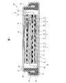
- FIG. 1 is a cross-sectional view showing the structure of the coin battery 101 according to the first embodiment.
- the coin battery 101 includes laminates 1 to 3, a positive electrode current collector group 4, a negative electrode current collector group 5, a pressure member 6, a metal case 7, and a metal.
- a sealing plate 8 and a gasket 9 are provided.
- the lower side is the positive electrode side of the coin battery 101
- the upper side is the negative electrode side of the coin battery 101.
- the laminates 1 to 3, the positive electrode current collector group 4, the negative electrode current collector group 5 and the pressing member 6 are drawn at a distance from each other for convenience, they are adjacent to each other. Contact with The later-described FIGS. 3 and 5 to 9 are also drawn similarly to FIG.
- the metal case 7 is formed of metal, and has a circular flat plate portion 71 and a side wall portion 72.
- the side wall portion 72 is formed to be bent from the outer peripheral portion of the flat plate portion 71.
- the end edge portion of the side wall portion 72 is curved toward the inside of the coin battery 101 to form a circular opening portion 73.
- the metal sealing plate 8 is formed of metal and has a circular flat plate portion 81 and a side wall portion 82.
- the flat plate portion 81 is formed smaller than the opening 73 of the metal case 7.
- the side wall portion 82 is formed to be bent from the outer peripheral portion of the flat plate portion 81.
- the edge of the side wall 82 is folded to the outer peripheral surface of the side wall 82.
- the end edges of the side wall portion 82 may not be folded.
- the sizes of the metal case 7 and the metal sealing plate 8 be appropriately selected in accordance with the use of the coin battery 101. Moreover, it is preferable that the material and the like of the metal case 7 and the metal sealing plate 8 be appropriately selected according to the temperature range in which the coin battery 101 is used.
- the gasket 9 is annularly formed of a resin having elasticity and insulating properties, and has an inner circumferential portion 91 and an outer circumferential portion 92.
- the inner circumferential portion 91 is along the inner circumferential surface of the side wall portion 82 of the metal sealing plate 8 between the inner surface of the flat plate portion 71 of the metal case 7 and the inner surface of the flat portion 81 of the metal sealing plate 8.
- the outer peripheral portion 92 is disposed so as to extend from the inner surface of the flat plate portion 71 of the metal case 7 to the outer peripheral surface of the flat plate portion 81 of the metal sealing plate 8 from the inner peripheral surface of the side wall portion 72 of the metal case 7 It is done.
- the outer peripheral portion 92 is not limited to such a structure.
- the end edge of the side wall portion 72 is curved so as to face the inside of the coin battery 101 as described above, so as to sandwich the side wall portion 82 of the metal sealing plate 8 and the outer peripheral portion 92 of the gasket 9.
- the side wall portion 82 is crimped.
- the metal case 7 (positive electrode) and the metal sealing plate 8 (negative electrode) are insulated, the metal case 7 and the metal sealing plate 8 are combined, and the metal case 7 and the metal seal are formed.
- the space between the plate 8 is sealed.
- a space sealed between the flat plate portion 71 of the metal case 7, the flat plate portion 81 of the metal sealing plate 8, and the inner circumferential portion 91 of the gasket 9 is formed.
- the laminates 1 to 3, the positive electrode current collector group 4, the negative electrode current collector group 5, and the pressure member 6 are disposed in this space.
- the pressing member 6 is a member for pressing the laminates 1 to 3, the positive electrode current collector group 4 and the negative electrode current collector group 5 which are stacked as described later.
- the pressure member 6 is constituted by a spring element such as a leaf spring, a shim or the like, and is formed of a conductive or insulating material. The pressure member 6 presses the laminates 1 to 3, the positive electrode current collector group 4 and the negative electrode current collector group 5 by their elastic force and brings them into close contact.
- the pressure member 6 is not provided for the purpose of applying a large pressure to the laminates 1 to 3, but the positive electrode current collector group 4, the negative electrode current collector group 5 and the metal case 7 or metal It is provided for the purpose of obtaining contact with the sealing plate 8 and for making constant the pressure applied to the laminates 1 to 3. Therefore, the shape of the pressure member 6 is not limited to a flat plate.
- the pressing member 6 may be a disc having a convex central portion or a hollow like a washer depending on the thickness of the laminates 1 to 3 or the deformed state of the metal case 7 after caulking or the like. It is necessary to select and use a member or even a corrugated washer.
- the laminates 1 to 3 are arranged in the order of the laminate 1, the laminate 2 and the laminate 3 from the positive electrode side.
- a positive electrode layer 11 (first electrode layer), a solid electrolyte layer 12, and a negative electrode layer 13 (second electrode layer) having a polarity opposite to that of the positive electrode layer 11 are stacked in this order.
- the positive electrode layer 11 is disposed closer to the flat plate portion 71 of the metal case 7.
- the negative electrode layer 13 is disposed closer to the flat plate portion 81 of the metal sealing plate 8.
- the solid electrolyte layer 12 is interposed between the positive electrode layer 11 and the negative electrode layer 13.
- a positive electrode layer 21 (first electrode layer), a solid electrolyte layer 22, and a negative electrode layer 23 (second electrode layer) having a polarity opposite to the polarity of the positive electrode layer 11 are stacked in this order.
- the positive electrode layer 21 is disposed on the side closer to the flat plate portion 81 of the metal sealing plate 8.
- the negative electrode layer 23 is disposed on the side closer to the flat plate portion 71 of the metal case 7.
- the solid electrolyte layer 22 is interposed between the positive electrode layer 21 and the negative electrode layer 23.
- a positive electrode layer 31 (first electrode layer), a solid electrolyte layer 32, and a negative electrode layer 33 (second electrode layer) having a polarity opposite to that of the positive electrode layer 11 are stacked in this order.
- the positive electrode layer 31 is disposed closer to the flat plate portion 71 of the metal case 7.
- the negative electrode layer 33 is disposed closer to the flat plate portion 81 of the metal sealing plate 8.
- the solid electrolyte layer 32 is interposed between the positive electrode layer 31 and the negative electrode layer 33.
- the laminates 1 and 2 are disposed such that the negative electrode layer 13 of the laminate 1 and the negative electrode layer 23 of the laminate 2 face each other.
- the laminates 2 and 3 are arranged such that the positive electrode layer 21 of the laminate 2 and the positive electrode layer 31 of the laminate 3 face each other.
- the positive electrode layer 11 of the laminate 1 and the positive electrode layer 31 of the laminate 3 are disposed on the same positive electrode side
- the negative electrode layer 13 of the laminate 1 and the negative electrode layer 33 of the laminate 3 are disposed on the same negative electrode side It is done.
- the positive electrode layer 21 of the laminate 2 and the positive electrode layers 11 and 31 of the laminates 1 and 3 are disposed on different sides, and the negative electrode layer 23 of the laminate 2 and the negative electrodes 13 and 33 of the laminates 1 and 3 are Located on different sides.
- the planar shape of the laminates 1 to 3 is ideally circular, but is not limited to circular as long as it can be stored in the above-mentioned sealed space.
- the planar shape of the laminates 1 to 3 may be a polygon, or a shape including straight lines and curves.
- the laminates 1 to 3 are all formed to have the same planar shape and the same size (area).
- the positive electrode layers 11, 21 and 31 are formed only of a mixture (mixture) of a positive electrode active material and a solid electrolyte, or a positive electrode active material.
- the weight ratio of the positive electrode active material to the solid electrolyte in the above mixture is, for example, 7: 3.
- materials generally used for the positive electrode active material in the all solid battery field can be used.
- a positive electrode active material used in the all solid state battery for example, lithium-containing oxide containing cobalt, nickel, and / or manganese (eg, lithium cobaltate (LiCoO 2 ), lithium nickelate (LiNiO 2 ), manganese, etc.
- Lithium such as spinel lithium manganate (such as LiMn 2 O 4 )), lithium nickel cobalt manganate (such as LiNi 1/3 Co 1/3 Mn 1/3 O 2 ), Li-rich complex oxide (Li 2)
- oxides such as MnO 3 -LiMO 2
- compounds other than oxides can also be mentioned.
- the compound other than an oxide e.g., olivine compounds (LiMPO 4), sulfur-containing compounds (Li 2 S, etc.) and the like.
- M represents a transition metal.
- the positive electrode active materials can be used singly or in combination of two or more.
- a lithium-containing oxide containing at least one selected from the group consisting of Co, Ni and Mn is preferable.
- the lithium-containing oxide may further contain a typical metal element such as Al.
- a lithium containing oxide containing Al aluminum containing nickel lithium cobaltate etc. are mentioned, for example.
- the negative electrode layers 13, 23, 33 are formed only of a mixture (mixture) of a negative electrode active material and a solid electrolyte, or only the negative electrode active material.
- the weight ratio of the negative electrode active material to the solid electrolyte in the above mixture is, for example, 6: 4.
- the negative electrode active material is not particularly limited as long as ions serving as charge carriers can be inserted and released depending on the type of the all solid battery, and a known negative electrode active material used in the all solid battery is used it can.
- a negative electrode active material for example, a carbonaceous material capable of inserting and desorbing lithium ions, and a single metal or semimetal capable of alloying and dealloying lithium ions , Alloys, or compounds.
- the carbonaceous material include graphite (natural graphite, artificial graphite and the like), hard carbon, amorphous carbon and the like.
- metals and semimetals alone and as alloys include lithium metals, alloys, and Si alone.
- the compound include oxides, sulfides, nitrides, hydrides, and silicides (such as lithium silicide).
- the oxide include titanium oxide, lithium titanium oxide, silicon oxide and the like.
- the negative electrode active material one type may be used alone, or two or more types may be used in combination. For example, silicon oxide and carbonaceous material may be used in combination.
- the solid electrolytes used for the positive electrode layers 11, 21, 31, the solid electrolyte layers 12, 22, 32 and the negative electrode layers 13, 23, 33 include an ion conductive inorganic solid electrolyte.
- the solid electrolyte particles can be plastically deformed to cause the solid electrolyte particles to be in close contact with each other.
- the adhesion between the solid electrolyte layer and the positive electrode layer and / or the negative electrode layer can be enhanced by plastic deformation of the solid electrolyte particles present in the vicinity of the surface of the solid electrolyte layer.
- the above-mentioned inorganic solid electrolyte is preferably a sulfide (a sulfide-based solid electrolyte) or a hydride (a hydride-based solid electrolyte).
- the hydride also generally includes a solid electrolyte called a complex hydride.
- the crystalline state of the solid electrolyte is not particularly limited, and may be either crystalline or amorphous.
- the sulfide containing Li and P is more preferable, for example.
- Specific examples of sulfides include Li 2 S-SiS 2 , Li 2 S-P 2 S 5 , Li 2 S-GeS 2 , Li 2 S-B 2 S 3 , and Li 2 S-Ga 2 S 3.
- Li 2 S-Al 2 S 3 Li 2 S-GeS 2 -P 2 S 5 , Li 2 S-Al 2 S 3 -P 2 S 5 , Li 2 S-P 2 S 3 , Li 2 S-P 2 S 3 -P 2 S 5, LiX-Li 2 S-P 2 S 5, LiX-Li 2 S-SiS 2, LiX-Li 2 S-B 2 S 3 (X: I, Br, Cl or I) Etc.
- the complex hydride of lithium borohydride etc. are mentioned, for example.
- the complex hydride include LiBH 4 -LiI complex hydride and LiBH 4 -LiNH 2 complex hydride, LiBH 4 -P 2 S 5 , LiBH 4 -P 2 I 4 and the like.
- the solid electrolyte may be used alone or in combination of two or more as needed.
- the solid electrolytes contained in the positive electrode and the negative electrode may be of the same type or may be different.
- the inorganic solid electrolyte may be used alone or in combination of two or more as needed.
- the solid electrolytes contained in the positive electrode layer and the negative electrode layer may be of the same type or may be different.
- the positive electrode current collector group 4 is configured of positive electrode current collectors 41 and 42 connected to each other.
- the positive electrode current collector 41 is disposed between the flat plate portion 71 of the metal case 7 and the positive electrode layer 11 of the laminate 1 so as to be in contact with both.
- the positive electrode current collector 42 is disposed between the positive electrode layer 21 of the laminate 2 and the positive electrode layer 31 of the laminate 3 so as to be in contact with both.
- the positive electrode current collector group 4 is electrically connected to the metal case 7.
- the negative electrode current collector group 5 is composed of negative electrode current collectors 51 and 52 connected to each other.
- the negative electrode current collector 51 is disposed between the pressing member 6 and the negative electrode layer 33 of the laminate 3.
- the negative electrode current collector 51 is in contact with the negative electrode layer 33 almost entirely, and is in contact with the metal sealing plate 8 at one end.
- the negative electrode current collector 52 is disposed between the negative electrode layer 13 of the laminate 1 and the negative electrode layer 23 of the laminate 2 so as to be in contact with both. Further, one end portion of the negative electrode current collector 52 is in contact with the metal sealing plate 8.
- the positive electrode current collector group 4 and the negative electrode current collector group 5 are made of copper, magnesium, stainless steel, titanium, iron, cobalt, nickel, zinc, aluminum, germanium, indium, lithium, tin, or an alloy of any of these. It is formed as a material.
- the form of the positive electrode current collector group 4 and the negative electrode current collector group 5 is a plate, a foil, a film, or the like.
- each of the positive electrode current collector group 4 and the negative electrode current collector group 5 a current collection point is provided in each of the positive electrode current collectors 41 and 42 and the negative electrode current collectors 51 and 52. It is also good. Further, the current collection points in the positive electrode current collector group 4 and the negative electrode current collector group 5 do not have to be provided 180 ° apart around the center of the coin battery 101.
- a binder for example, a conductive additive, other additives, and the like may be added to each electrode.
- the structure in which the positive electrode current collector group 4 is electrically connected to the metal case 7 and the structure in which the negative electrode current collector group 5 is electrically connected to the metal sealing plate 8 The case 7 is a positive electrode, and the metal sealing plate 8 is a negative electrode.
- the positive electrode layers 11, 21 and 31 are mutually connected by the positive electrode current collector group 4
- the negative electrode layers 13, 23 and 33 are mutually connected by the negative electrode current collector group 5.
- coin-type battery 101 is an all solid lithium ion secondary battery
- sufficient voltage can be secured without connecting stacks 1 to 3 in series.
- the stacks 1 to 3 may be connected in series.
- series and parallel may be combined internally. For example, the number of stacks may be increased to adopt a connection configuration such as 2-series 2-parallel or 2-series 3-parallel.
- coin-type battery 101 of the present embodiment includes the laminates 1 to 3, the number of laminates is not limited to three. Further, coin-type battery 101 has a structure of an odd numbered layer in which three layers of laminates 1 to 3 are stacked. On the other hand, coin battery 101 may have a structure having a stack of even layers. In this structure, the positive electrode layer is the one that faces the flat plate portion 81 of the metal sealing plate 8 in the stack of the uppermost layer. Therefore, it is necessary to provide an insulator (not shown) between the positive electrode layer and the metal sealing plate 8. The insulator may be disposed on either the metal sealing plate 8 side of the pressure member 6 or the positive electrode layer side. Alternatively, the pressure member may play the role of an insulator.
- FIG. 2 is a view showing a film forming method of the laminates 1 to 3 of the coin battery 101 according to the first embodiment.
- the powder film-forming method for example, electrostatic coating and electrostatic screen film-forming method (printing method)
- the laminated body of the coin-type battery which concerns on other embodiment mentioned later is also formed by the following film-forming methods.
- laminates 1 to 3 are produced by an electrostatic screen film formation method.
- FIG. 2 an apparatus shown in FIG. 2 is used.
- This apparatus comprises a porous screen 201 and a substrate B which is a pedestal on which a substrate to be film-formed is placed.
- the negative electrode of the DC power source DC is connected to the screen 201, and the substrate B is a positive electrode of the DC power source DC. Is connected.
- the positive electrode of the DC power supply DC may be connected to the screen 201, and the negative electrode of the DC power supply DC may be connected to the pedestal B.
- it since it suffices to generate a potential difference between the screen 201 and the printed material, it is not necessary to connect one to the positive electrode and not to connect the other to the negative electrode, and one may be the ground (earth) potential. .
- a commercially available mesh for screen printing can be used.
- the powder can be formed into an arbitrary shape by appropriately changing the opening shape of the mesh.
- a mesh having a mesh number of 300 / inch, a wire diameter of 30 ⁇ m, and an opening of 55 ⁇ m was employed.
- the material of the mesh is not limited as long as it has conductivity.
- the above mesh employed in the present embodiment is a general SUS mesh.
- the mesh used as the screen 201 it is preferable to appropriately select the number of meshes, the wire diameter, the opening, the material, and the like according to the powder and the environment.
- the distance between the screen 201 and the substrate B was 10 mm, and the applied voltage was 8 kV.
- the powder 202 is brought into contact with the screen 201 by imprinting the powder 202 onto the screen 201 by the imprinting body 203. Thereby, the powder 202 is charged. When the charged powder 202 falls through the screen 201, it is electrostatically induced to adhere to the substrate. In this manner, the positive electrode layers 11, 21, 31, the solid electrolyte layers 12, 22, 32 and the negative electrode layers 13, 23, 33 of the laminates 1 to 3 are formed.
- the positive electrode layers 11, 21, and 31 are formed of a positive electrode mixture layer, and the negative electrode layers 13, 23, and 33 are formed of a negative electrode mixture layer. Therefore, mixing of the positive electrode active material, which is a forming material of the positive electrode mixture layer, and the solid electrolyte, and mixing of the negative electrode active material, which is a forming material of the negative electrode mixture layer, and the solid electrolyte are performed.
- the production of the laminates 1 to 3 is not limited to the order of film formation described above, and film formation may be started from any layer.
- the positive electrode mixture layer, the solid electrolyte layer, and the negative electrode mixture layer after film formation may be respectively pressurized and flattened.
- pressure treatment is performed on each of the laminates 1 to 3 manufactured as described above.
- temporary pressure is applied to the stacks 1 to 3 under a reduced pressure environment.
- a pressure of 4 MPa (1 to 5 MPa) is applied to the laminates 1 to 3 for 3 seconds.
- This temporary pressurization may not necessarily be performed, but is preferably performed to eliminate gas and voids inside the laminates 1 to 3 formed as powder layers.
- the positive electrode layers 11, 21, 31, the solid electrolyte layers 12, 22, 32, and the negative electrode layers 13, 23, 33 are firmly integrated in the laminates 1 to 3 compressed by the above pressure.
- the thickness of each layer of the solid electrolyte layers 12, 22 and 32 is about several ⁇ m to 100 ⁇ m.
- the weight of each layer, the thickness of each layer, or the ratio of weight between each layer in laminates 1 to 3 is not limited to a specific range.
- the solid electrolyte layers 12, 22, and 32 be formed as thin as possible.
- the average thickness of the solid electrolyte layers 12, 22 and 32 is 5 ⁇ m or more and 100 ⁇ m or less, preferably 5 ⁇ m or more and 70 ⁇ m or less, and more preferably 5 ⁇ m or more and 30 ⁇ m or less.
- ratio of the thickness of negative electrode layer 13,23,33 with respect to the thickness of positive electrode layer 11,21,31 is 1.0 or more.
- the laminates 1 to 3 manufactured as described above, and the positive electrode current collector group 4 and the negative electrode current collector group 5 are stacked as shown in FIG. 1 (stacking step).
- the positive electrode current collectors 41 of the positive electrode current collector group 4 are stacked, and the laminate 1 is stacked on the positive electrode current collector 41 so that the positive electrode layer 11 faces the positive electrode current collector 41.
- the negative electrode current collector 52 of the negative electrode current collector group 5 is stacked on the negative electrode layer 13 of the laminate 1.
- the laminate 2 is superimposed on the negative electrode current collector 52 so that the negative electrode layer 23 faces the negative electrode current collector 52.
- the positive electrode current collector 42 of the positive electrode current collector group 4 is superimposed on the positive electrode layer 21 of the laminate 2.
- the laminate 3 is superimposed on the positive electrode current collector 42 so that the positive electrode layer 31 faces the positive electrode current collector 42.
- the negative electrode current collector 51 of the negative electrode current collector group 5 is superimposed on the negative electrode layer 33 of the laminate 3.
- a composite laminate in which the laminates 1 to 3 and the positive electrode current collector group 4 and the negative electrode current collector group 5 are laminated is produced.
- the stacking order described above may be reversed.
- Aluminum foil was used for the positive electrode current collectors 41 and 42, and copper foil was used for the negative electrode current collectors 51 and 52. In any case, it is preferable to select a material having a certain degree of toughness and rigidity.
- the positive electrode current collectors 41 and 42 and the negative electrode current collectors 51 and 52 are formed of individual metal foils, for example, they may be formed continuously by folding back the metal foil.
- the positive electrode current collector group 4 is connected to the flat plate portion 71 and the negative electrode current collector group 5 is formed into the flat plate portion 81 prior to the above-described laminate being sealed in the metal case 7 and the metal sealing plate 8.
- Connect to These connections are performed by welding such as ultrasonic welding and laser welding, but may be performed by methods other than welding.
- the conductive adhesive may be used for connection.
- a commercially available carbon-based conductive adhesive or conductive ink can be used as the conductive adhesive.
- the conductive adhesive and the conductive paint those containing gold or silver as conductive particles can be used.
- the pressure member 6 is disposed on the inner surface of the flat plate portion 81 of the metal sealing plate 8, and the composite laminate is disposed on the pressure member 6.
- the metal case 7 is superimposed on the metal sealing plate 8 with the gasket 9 interposed therebetween, and the end edge portion of the side wall portion 72 of the metal case 7 is crimped by pressure (encapsulation step).
- the metal case 7 and the metal sealing plate 8 are combined, and the space in which the composite laminate and the pressure member 6 are stored is sealed.
- the lamination of the laminates 1 to 3 with the positive electrode current collector group 4 and the negative electrode current collector group 5 is performed outside the metal sealing plate 8 as described above, but on the metal sealing plate 8. You may go.
- the stacked laminates 1 to 3 and the positive electrode current collector group 4 and the negative electrode current collector group 5 are sealed in the inside of the metal case 7 and the metal sealing plate 8. The same applies to the coin-type battery 102 (see FIG. 3) of the second embodiment described later.
- the pressure member 6 is basically disposed between the flat plate portion 81 of the metal sealing plate 8 and the negative electrode current collector 51.
- the metal case 7 and the metal sealing plate 8 can be made as long as the pressure member 6 can apply pressure to the laminate including the laminates 1 to 3, the positive electrode current collector group 4 and the negative electrode current collector group 5. It may be disposed at any position within the enclosed space formed by
- the pressure member 6 may be disposed between the flat plate portion 71 of the metal case 7 and the positive electrode current collector 41, or may be disposed at an arbitrary position in the above-described laminate. The same applies to the coin-type battery 102 (see FIG. 3) of the second embodiment described later.
- the laminates 1 to 3 in the coin battery 101 are densified by pressure molding, and the solid electrolyte layers 12, 22 and 32 are thinned. Thereby, the internal resistance of the laminates 1 to 3 is reduced. Therefore, the coin-type battery 101 can obtain a sufficiently large output without always applying a large pressure to the stacks 1 to 3 connected to each other.
- the laminates 1 to 3 are thinly formed by compression under pressure, the coin-type battery 101 is thinned, and more layers can be stacked inside the coin can with limited capacity to achieve higher capacity. Can be
- the pressing member 6 incorporated in the coin-type battery 101 is to obtain contact between the positive electrode current collector group 4 and the negative electrode current collector group 5 and the metal case 7 or the metal sealing plate 8.
- the pressure applied to the laminates 1 to 3 can be made constant.
- the pressing member 6 does not require a large pressing force for pressing the battery element like the elastic body (spring) of the coin battery disclosed in Patent Document 3. Therefore, the metal case 7 and the metal sealing plate 8 are not required to have high rigidity, and the metal case 7 and the metal sealing plate 8 do not have to be thick. Therefore, it is possible to reduce the weight and the size of the coin battery 101.
- the pressing member 6 may not be used if it is unnecessary. For example, when the inside of the coin can consisting of the metal case 7 and the metal sealing plate 8 is filled only with the electrode layer and the current collector, the contact between the coin can and the current collector can be sufficiently obtained without the pressing member. The pressing member 6 becomes unnecessary.
- FIG. 3 is a cross-sectional view showing the structure of the coin battery 102 according to the second embodiment.
- the coin battery 102 is the same as the coin battery 101 of the first embodiment, including three laminates 1 to 3, a pressure member 6, a metal case 7, and a metal sealing plate 8. And a gasket 9. Further, the coin battery 102 includes the positive electrode current collector group 4A, the negative electrode current collector group 5A, and the separators 10 and 20 (insulators). Further, in the coin battery 102, the laminates 1 to 3 are arranged such that the positive electrode layers 11, 21 and 31 are on the side wall 72 side of the metal case 7.
- a positive electrode current collector 43 is further added to the positive electrode current collector group 4 in the coin battery 101.
- a negative electrode current collector 53 is further added to the negative electrode current collector group 5 of the coin battery 101.
- the positive electrode current collector 42 is disposed between the laminates 1 and 2 so as to be in contact with the positive electrode layer 21 of the laminate 2.
- the positive electrode current collector 43 is disposed between the laminates 2 and 3 so as to be in contact with the positive electrode layer 31 of the laminate 3.
- the negative electrode current collector 52 is disposed between the stacked bodies 2 and 3 so as to be in contact with the negative electrode layer 23 of the stacked body 2.
- the negative electrode current collector 53 is disposed between the laminates 1 and 2 so as to be in contact with the negative electrode layer 13 of the laminate 1.
- the separator 10 is formed of an insulating material, and is disposed between the positive electrode current collector 42 and the negative electrode current collector 53. Thereby, the separator 10 electrically insulates the positive electrode current collector 42 and the negative electrode current collector 53.
- the separator 20 is formed of an insulating material, and is disposed between the positive electrode current collector 43 and the negative electrode current collector 52. Thereby, the separator 10 electrically insulates the positive electrode current collector 43 and the negative electrode current collector 52.
- the coin-type battery 102 of the present embodiment also includes the laminates 1 to 3 as in the above-described coin-type battery 101, but the number of laminates is not limited to three.
- the coin-type battery 102 also has an odd-numbered layer structure in which three-layered laminates 1 to 3 are stacked.
- coin-type battery 102 may have a structure having a stack of even layers.
- the negative electrode layer is the one facing the flat plate portion 81 of the metal sealing plate 8 in the stack of the uppermost layer. For this reason, in the coin battery 102, unlike the coin battery 101, it is not necessary to provide an insulator between the negative electrode layer and the metal sealing plate 8.
- the production of the laminates 1 to 3 is performed in the same manner as the coin-type battery 101 of the first embodiment, and thus the description thereof is omitted here.
- the manufactured laminates 1 to 3 and the positive electrode current collector group 4A and the negative electrode current collector group 5A are stacked as shown in FIG.
- the positive electrode current collector 41 of the positive electrode current collector group 4A is stacked, and the laminate 1 is stacked on the positive electrode current collector 41 so that the positive electrode layer 11 faces the positive electrode current collector 41.
- the negative electrode layer 13 of the laminate 1 the negative electrode current collector 53 of the negative electrode current collector group 5A, the separator 10, and the positive electrode current collector 42 of the positive electrode current collector group 4A are stacked in this order.
- the laminate 2 is superimposed on the positive electrode current collector 42 so that the positive electrode layer 21 faces the positive electrode current collector 42.
- the negative electrode current collector 52 of the negative electrode current collector group 5A, the separator 20, and the positive electrode current collector 43 of the positive electrode current collector group 4A are stacked in this order on the negative electrode layer 23 of the laminate 2.
- the laminate 3 is superimposed on the positive electrode current collector 43 so that the positive electrode layer 31 faces the positive electrode current collector 43.
- the negative electrode current collector 51 of the negative electrode current collector group 5A is superimposed on the negative electrode layer 33 of the laminate 3.
- the pressure member 6 is disposed on the inner surface of the flat plate portion 81 of the metal sealing plate 8, and the above-described composite laminate is disposed on the pressure member 6.
- the metal case 7 is superposed on the metal sealing plate 8 with the gasket 9 interposed therebetween, and the end edge portion of the side wall portion 72 in the metal case 7 is caulked by pressure.
- the metal case 7 and the metal sealing plate 8 are combined, and the space in which the composite laminate and the pressure member 6 are stored is sealed.
- the internal resistances of the stacks 1 to 3 are reduced by being pressurized.
- the coin-type battery 103 can ensure a sufficiently large output.
- FIG. 4 is a perspective view showing the internal structure of the coin battery 103 according to the third embodiment.
- FIG. 5 is a cross-sectional view showing the internal structure of the coin battery 103 according to the third embodiment.
- FIG. 6 is a cross-sectional view showing another internal structure of the coin battery 103 according to the third embodiment.
- the coin-type battery 103 shown in FIG. 4 has a structure in which the electrode layer stack 70 is covered by the insulating cover 60. Although not shown, this structure is contained (encapsulated) in an outer package formed by the metal case 7 and the metal sealing plate 8 provided in the coin battery 101 (see FIG. 1) of the first embodiment described above. There is.
- the electrode layer laminate 70 has a structure in which a laminate of four layers and a positive electrode current collector group and a negative electrode current collector group connected to each of the four layer laminate are laminated.
- the insulating covering 60 is a covering formed of a glass-based, resin-based or ceramic-based insulating material, and covers the outer peripheral side surface of the electrode layer laminate 70.
- the insulating covering 60 may be formed by applying an insulating material to the side surface of the electrode layer stack 70 and drying it, or it is designed in a case shape that can cover the electrode layer stack 70. And may be produced.
- the insulating covering 60 shown in FIG. 4 is formed in the shape of a case, and has a planar shape consisting of two parallel straight lines and two curves located on both sides of the straight lines. Such an insulation covering 60 is formed in accordance with the shape of the electrode layer laminate 70.
- the current collection opening 60a for collecting current by the positive electrode current collector group is disposed at the arrangement position (current collecting point) of each positive electrode current collector of the positive electrode current collector group. It is provided at the corresponding position.
- the positive electrode current collector portion 40 electrically connected to the positive electrode current collector group is provided on the side surface.
- current collection opening 60a for current collection by the negative electrode current collector group is the arrangement position of each negative electrode current collector of the negative electrode current collector group (current collection It is provided in the position according to the part).
- a negative electrode current collector 50 electrically connected to the negative electrode current collector group is provided on the side surface.
- the insulating covering 60 covers each laminate around the current collecting portion, and connects the positive electrode current collector and the positive electrode current collector 40 and the negative electrode current collector and the negative electrode current collector 50. It has a current collection opening 60a for connection. Thereby, the connection portion between the positive electrode current collector and the positive electrode current collector portion 40 is short-circuited with the negative electrode layer of the laminate, and the connection portion between the negative electrode current collector and the negative electrode current collector portion 50 is the positive electrode layer It is possible to prevent short circuit.
- the insulating covering 60 when the coin-shaped battery 103 is subjected to strong vibration, it is possible to prevent the laminates from being broken.
- the electrode layer laminate 70 may have a structure provided with a three-layer laminate. The structure will be described below.
- the electrode layer laminate 70 shown in FIG. 5 is applied to a coin battery 101, and has a structure in which laminates 1 to 3, a positive electrode current collector group 4 and a negative electrode current collector group 5 are stacked.
- the positive electrode current collecting portion 40 is connected to the positive electrode current collectors 41 and 42 of the positive electrode current collector group 4 by inserting a part thereof into the current collection opening 60 a of the insulating covering 60.
- the negative electrode current collector portion 50 is connected to the negative electrode current collectors 51 and 52 of the negative electrode current collector group 5 by inserting a part thereof into the current collection opening 60 a of the insulating covering 60.
- the electrode layer laminate 70A shown in FIG. 6 is applied to a coin battery 102, and has a structure in which laminates 1 to 3, a positive electrode current collector group 4A, and a negative electrode current collector group 5A are stacked.
- the positive electrode current collecting portion 40A is connected to the positive electrode current collectors 41 to 43 of the positive electrode current collector group 4A by inserting a part thereof into the current collection opening 60a of the insulating covering 60.
- the negative electrode current collector portion 50A is connected to the negative electrode current collectors 51 to 53 of the negative electrode current collector group 5A by inserting a part thereof into the current collection opening 60a of the insulating covering 60.
- Coin batteries 101 to 103 are charged to a charge termination voltage of 4.7 V at a current of 0.05 mA / cm 2 in a thermostatic chamber maintained at 25 ° C., and then discharged at a current of 0.05 mA / cm 2. It discharged to the end voltage 2.8V.
- the charge capacity and the discharge capacity (first charge and discharge capacity) of each of the coin batteries 101 to 103 at this time are shown in Table 1.
- any of the coin batteries 101 to 103 having different current collection structures operate as batteries that can withstand practical use.
- Embodiment 4 The fourth embodiment of the present invention is described below with reference to FIG. In the present embodiment, components having the same functions as the components in the first embodiment will be denoted by the same reference numerals, and the description thereof will be omitted.
- FIG. 7 is a cross-sectional view showing the structure of the coin battery 104 according to the fourth embodiment.
- the coin-type battery 104 is the same as the coin-type battery 101 of Embodiment 1 in the positive electrode current collector group 4, the negative electrode current collector group 5, the pressure member 6, and the metal case 7. And a metal sealing plate 8 and a gasket 9. Further, the coin-type battery 104 is provided with stacks 1B to 3B.
- the positive electrode layer 111 (first electrode layer), the solid electrolyte layer 12, and the negative electrode layer 13 (second electrode layer) having a polarity opposite to the polarity of the positive electrode layer 111 are stacked in this order. Is made up of The positive electrode layer 111 is disposed closer to the flat plate portion 71 of the metal case 7. The positive electrode layer 111 is formed such that the area of the layer surface (the surface in contact with the solid electrolyte layer 12) is smaller than the area of the layer surface of the solid electrolyte layer 12 (the surface in contact with the positive electrode layer 111).
- the positive electrode layer 111 is formed on the solid electrolyte layer 12 so that the outer peripheral side surface portion (portion of the outer peripheral side surface) is positioned inside the outer peripheral side surface portion of the solid electrolyte layer 12.
- the area of the negative electrode layer 13 is equal to the area of the solid electrolyte layer 12.
- the positive electrode layer 211 (first electrode layer), the solid electrolyte layer 22, and the negative electrode layer 23 (second electrode layer) having a polarity opposite to the polarity of the positive electrode layer 111 are stacked in this order.
- Is made up of The positive electrode layer 211 is disposed on the side closer to the flat plate portion 81 of the metal sealing plate 8.
- the positive electrode layer 211 is formed such that the area of the layer surface (the surface in contact with the solid electrolyte layer 22) is smaller than the area of the layer surface of the solid electrolyte layer 22 (the surface in contact with the positive electrode layer 211).
- the positive electrode layer 211 is formed on the solid electrolyte layer 22 such that the outer peripheral side surface portion thereof is positioned inside the outer peripheral side surface portion of the solid electrolyte layer 22.
- the area of the negative electrode layer 23 is equal to the area of the solid electrolyte layer 22.
- the positive electrode layer 311 (first electrode layer), the solid electrolyte layer 32, and the negative electrode layer 33 (second electrode layer) having a polarity opposite to the polarity of the positive electrode layer 111 are stacked in this order. Is made up of The positive electrode layer 311 is disposed closer to the flat plate portion 71 of the metal case 7. The positive electrode layer 311 is formed such that the area of the layer surface (the surface in contact with the solid electrolyte layer 32) is smaller than the area of the layer surface of the solid electrolyte layer 32 (the surface in contact with the positive electrode layer 311).
- the positive electrode layer 311 is formed on the solid electrolyte layer 32 so that the outer peripheral side surface portion thereof is positioned inside the outer peripheral side surface portion of the solid electrolyte layer 32.
- the area of the negative electrode layer 33 is equal to the area of the solid electrolyte layer 32.
- the laminates 1B and 2B are arranged such that the negative electrode layer 13 of the laminate 1 and the negative electrode layer 23 of the laminate 2 face each other.
- the laminates 2B and 3B are arranged such that the positive electrode layer 211 of the laminate 2B and the positive electrode layer 311 of the laminate 3B face each other.
- the positive electrode layer 111 of the laminate 1B and the positive electrode layer 311 of the laminate 3B are disposed on the same side
- the negative electrode layer 13 of the laminate 1B and the anode layer 33 of the laminate 3B are disposed on the same side.
- the positive electrode layer 211 of the laminate 2B and the positive electrodes 111 and 311 of the laminates 1B and 3B are disposed on different sides, and the negative electrode layer 23 of the laminate 2B and the negative electrodes 13 and 33 of the laminates 1B and 3B are Located on different sides.
- the positive electrode layers 11, 21 and 31 of the laminates 1 to 3 in the coin-shaped battery 101 of Embodiment 1 are replaced with the positive electrode layers 111, 211 and 311, respectively. is there. Therefore, the coin battery 104 is configured the same as the coin battery 101 except for the above.
- the positive electrode layers 111, 211, and 311 are formed of the same material as the positive electrode layers 11, 21, and 31 in the coin battery 101 of the first embodiment.
- the coin battery 104 configured as described above is manufactured by the same manufacturing method as the coin battery 101 of the first embodiment.
- positive electrode layers 111, 211, and 311 are formed such that the area of the surface is smaller than the area of the surface of solid electrolyte layer 12, and the outer peripheral side surface is solid. It is formed so as to be located inside the outer peripheral side portions of the electrolyte layers 12, 22, 32.
- the outer peripheral side surface portions of the positive electrode layers 111, 211, 311 and the negative electrode layers 13, 23, 33 may be broken due to vibration, excessive load, etc. to which the coin-type battery 104 is subjected at the time of manufacture and use.
- the coin-type battery 104 is small, it is susceptible to vibration because it is often mounted and used in a portable device.
- the positive electrode layers 111, 211, 311 as described above, the positive electrode layers 111, 211, 311 and the negative electrode layers 13, 23, 33 are respectively inserted via the broken powder material. Shorting can be suppressed. Therefore, the product yield and product reliability of coin-type battery 104 can be greatly improved.
- the areas of the surface portions of the positive electrode layers 111, 211, and 311 are equal to the area of the surface portions of the negative electrode layers 13, 23, 33, respectively.
- the area may be larger than the area of the surface portions of the positive electrode layers 111, 211, 311 and the negative electrode layers 13, 23, 33. Even with this configuration, it is possible to suppress the short circuit between the positive electrode layers 111, 211, 311 and the negative electrode layers 13, 23, 33, respectively.
- the configuration of the present embodiment is applicable to the coin battery 101 of Embodiment 1 as shown in FIG. 7, it is also applicable to the coin batteries 102 and 103 of Embodiments 2 and 3 respectively. It is.
- the positive electrode layers 111, 211, and 311 (positive electrode mixture layer) are formed, and the solid electrolyte layers 12, 22 are formed thereon, respectively.
- 32 are formed, and the negative electrode layers 13, 23, 33 (negative electrode mixture layer) are formed thereon.
- the coin-type battery 104 of the present modification first, the negative electrode layers 13, 23 and 33 are formed, and the solid electrolyte layers 12, 22 and 32 are formed thereon. And the positive electrode layers 111, 211 and 311 are formed thereon.
- FIG. 8 is a cross-sectional view showing the structure of the coin battery 105 according to the fifth embodiment.
- the coin battery 105 is the same as the coin battery 104 of the fourth embodiment, and includes a positive electrode current collector group 4, a negative electrode current collector group 5, a pressure member 6, and a metal case 7. And a metal sealing plate 8 and a gasket 9. Further, the coin battery 105 is provided with the laminates 1C to 3C.
- the laminate 1C is configured by stacking the positive electrode layer 111, the solid electrolyte layer 121, and the negative electrode layer 13 in this order.
- the solid electrolyte layer 121 is formed to cover the outer peripheral side surface portion of the positive electrode layer 111.
- the laminate 2C is configured by stacking the positive electrode layer 211, the solid electrolyte layer 221, and the negative electrode layer 23 in this order.
- the solid electrolyte layer 221 is formed to cover the outer peripheral side surface portion of the positive electrode layer 211.
- the laminate 3C is configured by laminating the positive electrode layer 311, the solid electrolyte layer 321, and the negative electrode layer 33 in this order.
- the solid electrolyte layer 321 is formed to cover the outer peripheral side surface portion of the positive electrode layer 311.
- the coin battery 105 configured as described above is manufactured by the same manufacturing method as the coin battery 101 of the first embodiment.
- the laminates 1C to 3C are obtained by replacing the solid electrolyte layers 12, 22 and 32 of the laminates 1B to 3B in the coin battery 104 of Embodiment 4 with solid electrolyte layers 121, 221 and 321, respectively. . Therefore, the coin battery 105 is configured the same as the coin battery 104 except for the above.
- the solid electrolyte layers 121, 221 and 321 are formed of the same material as the solid electrolyte layers 12, 22 and 32 in the coin battery 101 of the first embodiment.
- solid electrolyte layers 121, 221, and 321 are formed to cover outer peripheral side portions of positive electrode layers 111, 211, and 311, respectively. Thereby, the outer peripheral side surface portions of the positive electrode layers 111, 211, 311 can be prevented from being broken. Also, there is a possibility that the positive electrode layers 111, 211, 311 and the negative electrode layers 13, 23, 33 may be short-circuited through the powder material generated by the outer peripheral side portions of the negative electrode layers 13, 23, 33 being broken. The number can be further reduced as compared with the coin-type battery 104 of the fourth aspect. Therefore, the product yield and product reliability of coin-type battery 104 can be further improved.
- the configuration of the present embodiment can be applied to the coin-type battery 101 of the first embodiment similarly to the coin-type battery 104 of the fourth embodiment, but the coin-type batteries 102 and 103 of the second and third embodiments are also applicable. Each is applicable.
- a comparative example is prepared, and the yield is compared with the coin batteries 104 and 105.
- the coin-type battery of the comparative example has the same configuration as the coin-type battery 105 except that the areas and shapes of the positive electrode layer, the solid electrolyte layer, and the negative electrode layer are the same.
- the positive electrode layer, the solid electrolyte layer, and the negative electrode layer that constitute the laminate are formed by stacking the layers in the same area.
- coin-type batteries 104 and 105 are charged to a charge termination voltage of 4.7 V with a current of 0.05 mA / cm 2 in a thermostatic chamber maintained at 25 ° C., and then a current of 0.0 mA / cm 2 Discharge to a discharge end voltage of 2.8V.
- a current of 0.0 mA / cm 2 Discharge to a discharge end voltage of 2.8V.
- an initial charge capacity of 420 mAh / g was obtained, and an initial discharge capacity of 310 mAh / g was obtained.
- either coin cell 104, 105 operates as a practical battery.
- FIG. 9 is a cross-sectional view showing the structure of the coin battery 106 according to the sixth embodiment.
- a coin battery 106 is the same as the coin battery 104 of the fourth embodiment, and includes a positive electrode current collector group 4, a negative electrode current collector group 5, a pressure member 6, and a metal case 7. And a metal sealing plate 8 and a gasket 9. Further, the coin battery 106 is provided with stacked bodies 1D to 3D.
- the negative electrode layer 132 (first electrode layer), the solid electrolyte layer 122, and the positive electrode layer 112 (second electrode layer) having a polarity opposite to the polarity of the negative electrode layer 132 are stacked in this order.
- Is made up of The solid electrolyte layer 122 is formed between the positive electrode layer 112 and the negative electrode layer 132 so as to cover the outer peripheral side surface of the negative electrode layer 132.
- the positive electrode layer 112 is formed such that the area of the layer surface (the surface in contact with the solid electrolyte layer 122) is smaller than the area of the layer surface of the solid electrolyte layer 122 (the surface in contact with the positive electrode layer 112).
- the positive electrode layer 112 is formed such that the area of the layer surface is smaller than the area of the layer surface of the negative electrode layer 132 (the surface in contact with the solid electrolyte layer 122).
- the positive electrode layer 112 is formed on the solid electrolyte layer 122 so that the outer peripheral side surface portion thereof is positioned inside the outer peripheral side surface portion of the solid electrolyte layer 122.
- the negative electrode layer 232 (first electrode layer), the solid electrolyte layer 222, and the positive electrode layer 212 (second electrode layer) having a polarity opposite to the polarity of the negative electrode layer 232 are stacked in this order Is made up of
- the solid electrolyte layer 222 is formed between the positive electrode layer 212 and the negative electrode layer 232 so as to cover the outer peripheral side surface of the negative electrode layer 232.
- the positive electrode layer 212 is formed such that the area of the layer surface (the surface in contact with the solid electrolyte layer 222) is smaller than the area of the layer surface of the solid electrolyte layer 222 (the surface in contact with the positive electrode layer 212).
- the positive electrode layer 212 is formed such that the area of the layer surface is smaller than the area of the layer surface of the negative electrode layer 232 (the surface in contact with the solid electrolyte layer 222).
- the positive electrode layer 212 is formed on the solid electrolyte layer 222 such that the outer peripheral side surface portion thereof is positioned inside the outer peripheral side surface portion of the solid electrolyte layer 222.
- the negative electrode layer 332 (first electrode layer), the solid electrolyte layer 322, and the positive electrode layer 312 (second electrode layer) having a polarity opposite to the polarity of the negative electrode layer 332 are stacked in this order.
- Is made up of The solid electrolyte layer 322 is formed between the positive electrode layer 312 and the negative electrode layer 332 so as to cover the outer peripheral side surface of the negative electrode layer 332.
- the positive electrode layer 312 is formed such that the area of the layer surface (the surface in contact with the solid electrolyte layer 322) is smaller than the area of the layer surface of the solid electrolyte layer 322 (the surface in contact with the positive electrode layer 312).
- the positive electrode layer 312 is formed such that the area of the layer surface is smaller than the area of the layer surface of the negative electrode layer 332 (the surface in contact with the solid electrolyte layer 322).
- the positive electrode layer 312 is formed on the solid electrolyte layer 322 so that the outer peripheral side surface portion thereof is positioned inside the outer peripheral side surface portion of the solid electrolyte layer 322.
- the coin-type battery 106 configured as described above is manufactured by the same manufacturing method as the coin-type battery 101 of the first embodiment. However, in the laminates 1D to 3D, the negative electrode layers 132, 232 and 332 are formed respectively, and the solid electrolyte layers 122, 222 and 322 are formed on the negative electrode layers 132, 232 and 332, and the solid electrolyte layer 122, The positive electrode layers 1112, 212 and 312 are formed on the layers 222 and 322, respectively.
- the solid electrolyte layers 122, 222, 322 are formed of the same material as the solid electrolyte layers 12, 22, 32 in the coin battery 101 of Embodiment 1. Further, the positive electrode layers 112, 212, and 312 are formed of the same material as the positive electrode layers 11, 21, and 31 in the coin battery 101. The negative electrode layers 132, 232, 332 are formed of the same material as the negative electrode layers 13, 23, 33 in the coin battery 101.
- solid electrolyte layers 122, 222, and 322 are formed to cover the outer peripheral side portions of negative electrode layers 132, 232, and 332, respectively. Thereby, the outer peripheral side surface portions of the negative electrode layers 132, 232, 332 can be prevented from being broken. In addition, the possibility of short circuit between the positive electrode layers 112, 212 and 312 and the negative electrode layers 132, 232 and 332, respectively, is reduced through the powder material produced by the outer peripheral side surface portions of the positive electrode layers 112, 212 and 312 being broken. be able to. Therefore, the product yield and product reliability of coin battery 106 can be improved.
Landscapes
- Chemical & Material Sciences (AREA)
- Chemical Kinetics & Catalysis (AREA)
- Electrochemistry (AREA)
- General Chemical & Material Sciences (AREA)
- Engineering & Computer Science (AREA)
- Manufacturing & Machinery (AREA)
- Physics & Mathematics (AREA)
- Condensed Matter Physics & Semiconductors (AREA)
- General Physics & Mathematics (AREA)
- Inorganic Chemistry (AREA)
- Secondary Cells (AREA)
- Battery Electrode And Active Subsutance (AREA)
Abstract
L'invention concerne une batterie en forme de pièce (101) comprenant : un ou plusieurs stratifiés (1 à 3) constitués chacun par stratification d'une couche d'électrode positive (11, 21, 31), d'une couche d'électrolyte solide (12, 22, 32), et d'une couche d'électrode négative (13, 23, 33); et un boîtier externe qui est constitué d'un boîtier métallique (7) et d'une plaque d'étanchéité d'ouverture métallique (8) et dans laquelle la pluralité de stratifiés (1 à 3) sont étanchéifiés. Chaque stratifié (1 à 3) est comprimé par mise sous pression. L'épaisseur moyenne de la couche d'électrolyte solide (12, 22, 32) dans les stratifiés (1 à 3) respectifs est de 5 µm à 100 µm.
Priority Applications (4)
| Application Number | Priority Date | Filing Date | Title |
|---|---|---|---|
| EP18832038.6A EP3654438B1 (fr) | 2017-07-12 | 2018-07-05 | Batterie en forme de pièce et son procédé de production |
| KR1020207003958A KR102599733B1 (ko) | 2017-07-12 | 2018-07-05 | 코인형 전지 및 그 제조방법 |
| US16/628,452 US20210135276A1 (en) | 2017-07-12 | 2018-07-05 | Coin-shaped battery and method for producing same |
| CN201880045883.4A CN110870128A (zh) | 2017-07-12 | 2018-07-05 | 硬币形电池及其制造方法 |
Applications Claiming Priority (2)
| Application Number | Priority Date | Filing Date | Title |
|---|---|---|---|
| JP2017136561A JP6943656B2 (ja) | 2017-07-12 | 2017-07-12 | コイン形電池およびその製造方法 |
| JP2017-136561 | 2017-07-12 |
Publications (1)
| Publication Number | Publication Date |
|---|---|
| WO2019013084A1 true WO2019013084A1 (fr) | 2019-01-17 |
Family
ID=65002545
Family Applications (1)
| Application Number | Title | Priority Date | Filing Date |
|---|---|---|---|
| PCT/JP2018/025486 Ceased WO2019013084A1 (fr) | 2017-07-12 | 2018-07-05 | Batterie en forme de pièce et son procédé de production |
Country Status (6)
| Country | Link |
|---|---|
| US (1) | US20210135276A1 (fr) |
| EP (1) | EP3654438B1 (fr) |
| JP (1) | JP6943656B2 (fr) |
| KR (1) | KR102599733B1 (fr) |
| CN (1) | CN110870128A (fr) |
| WO (1) | WO2019013084A1 (fr) |
Cited By (1)
| Publication number | Priority date | Publication date | Assignee | Title |
|---|---|---|---|---|
| JP2021002495A (ja) * | 2019-06-24 | 2021-01-07 | トヨタ自動車株式会社 | 全固体電池および全固体電池システム |
Families Citing this family (13)
| Publication number | Priority date | Publication date | Assignee | Title |
|---|---|---|---|---|
| US9318107B1 (en) | 2014-10-09 | 2016-04-19 | Google Inc. | Hotword detection on multiple devices |
| US9812128B2 (en) | 2014-10-09 | 2017-11-07 | Google Inc. | Device leadership negotiation among voice interface devices |
| JP7168361B2 (ja) * | 2018-07-04 | 2022-11-09 | 株式会社Soken | 全固体電池 |
| JP7360820B2 (ja) * | 2019-05-30 | 2023-10-13 | 日立造船株式会社 | 二次電池およびその製造方法 |
| CN112753121B (zh) | 2019-08-29 | 2023-12-19 | 麦克赛尔株式会社 | 全固体电池 |
| EP4113730A4 (fr) * | 2020-02-27 | 2025-01-08 | NGK Insulators, Ltd. | Cellule secondaire en forme de pièce |
| JP2021136214A (ja) * | 2020-02-28 | 2021-09-13 | マクセルホールディングス株式会社 | 積層電極体、積層電極体を備えた全固体電池及び積層電極体の製造方法 |
| JP7548300B2 (ja) * | 2020-04-07 | 2024-09-10 | 株式会社村田製作所 | 固体電池 |
| KR102918561B1 (ko) | 2020-07-17 | 2026-01-27 | 주식회사 엘지에너지솔루션 | 버튼형 이차전지 및 그의 제조방법 |
| FR3146029A1 (fr) * | 2023-02-17 | 2024-08-23 | Psa Automobiles Sa | Systeme de maintien de pression mecanique pour electrode helicoidale |
| CN116845265A (zh) * | 2023-08-14 | 2023-10-03 | 常州宇峰电池有限公司 | 一种叠片式锂锰一次扣式电池及其制备方法 |
| KR20260036670A (ko) * | 2024-09-09 | 2026-03-17 | 삼성전기주식회사 | 전고체 전지 |
| CN119852294B (zh) * | 2025-01-07 | 2025-12-05 | 武汉理工大学 | 一种负极对称放置的扣式电池及其组装方法 |
Citations (7)
| Publication number | Priority date | Publication date | Assignee | Title |
|---|---|---|---|---|
| JPS5317195B2 (fr) | 1974-01-24 | 1978-06-06 | ||
| JP2010056067A (ja) | 2008-07-31 | 2010-03-11 | Idemitsu Kosan Co Ltd | コイン型リチウム二次電池 |
| JP2010282803A (ja) * | 2009-06-04 | 2010-12-16 | Idemitsu Kosan Co Ltd | 全固体リチウムイオン二次電池の製造方法 |
| WO2011064842A1 (fr) * | 2009-11-25 | 2011-06-03 | トヨタ自動車株式会社 | Processus de production de stratifié d'électrode et stratifié d'électrode |
| JP2011159413A (ja) | 2010-01-29 | 2011-08-18 | Panasonic Corp | コイン形電池 |
| US20170162901A1 (en) * | 2015-12-04 | 2017-06-08 | Quantumscape Corporation | Lithium, phosphorus, sulfur, and iodine including electrolyte and catholyte compositions, electrolyte membranes for electrochemical devices, and annealing methods of making these electrolytes and catholytes |
| WO2017104405A1 (fr) * | 2015-12-16 | 2017-06-22 | 富士フイルム株式会社 | Matériau pour électrodes, feuille d'électrode pour des batteries rechargeables tout solide, batterie rechargeable tout solide, procédé permettant de produire une feuille d'électrode pour des batteries rechargeables tout solide et procédé permettant de produire une batterie rechargeable tout solide |
Family Cites Families (10)
| Publication number | Priority date | Publication date | Assignee | Title |
|---|---|---|---|---|
| JP4355970B2 (ja) * | 1997-10-29 | 2009-11-04 | ソニー株式会社 | 固体電解質電池及びその製造方法 |
| DE69837744T2 (de) * | 1997-10-29 | 2008-01-10 | Sony Corp. | Sekundärbatterie mit nichtwässrigem Elektrolyten und Verfahren zu ihrer Herstellung |
| US20070134551A1 (en) * | 2005-12-14 | 2007-06-14 | Avestor Limited Partnership | Electrochemical battery and method for making same |
| KR20100056067A (ko) | 2008-11-19 | 2010-05-27 | 주식회사 큐리프 | 세곡수단 제어방법 |
| KR20100098543A (ko) * | 2008-12-01 | 2010-09-07 | 도요타지도샤가부시키가이샤 | 고체 전해질 전지, 차량, 전지 탑재 기기 및 고체 전해질 전지의 제조 방법 |
| WO2013153693A1 (fr) * | 2012-04-13 | 2013-10-17 | 株式会社村田製作所 | Électrolyte solide pour batterie solide à base de sulfure, électrodes, batterie solide à base de sulfure utilisant ceux-ci, et procédé de production de ladite batterie |
| CN105103332B (zh) * | 2013-03-18 | 2017-06-13 | 富士通株式会社 | 电子器件及其制造方法、以及网络系统 |
| JP6048396B2 (ja) * | 2013-12-26 | 2016-12-21 | トヨタ自動車株式会社 | 全固体電池の製造方法 |
| JP2016012495A (ja) * | 2014-06-30 | 2016-01-21 | トヨタ自動車株式会社 | リチウム固体二次電池およびその製造方法 |
| US10686213B2 (en) * | 2017-05-18 | 2020-06-16 | Panasonic Intellectual Property Management Co., Ltd. | Battery |
-
2017
- 2017-07-12 JP JP2017136561A patent/JP6943656B2/ja active Active
-
2018
- 2018-07-05 US US16/628,452 patent/US20210135276A1/en not_active Abandoned
- 2018-07-05 KR KR1020207003958A patent/KR102599733B1/ko active Active
- 2018-07-05 CN CN201880045883.4A patent/CN110870128A/zh active Pending
- 2018-07-05 EP EP18832038.6A patent/EP3654438B1/fr active Active
- 2018-07-05 WO PCT/JP2018/025486 patent/WO2019013084A1/fr not_active Ceased
Patent Citations (7)
| Publication number | Priority date | Publication date | Assignee | Title |
|---|---|---|---|---|
| JPS5317195B2 (fr) | 1974-01-24 | 1978-06-06 | ||
| JP2010056067A (ja) | 2008-07-31 | 2010-03-11 | Idemitsu Kosan Co Ltd | コイン型リチウム二次電池 |
| JP2010282803A (ja) * | 2009-06-04 | 2010-12-16 | Idemitsu Kosan Co Ltd | 全固体リチウムイオン二次電池の製造方法 |
| WO2011064842A1 (fr) * | 2009-11-25 | 2011-06-03 | トヨタ自動車株式会社 | Processus de production de stratifié d'électrode et stratifié d'électrode |
| JP2011159413A (ja) | 2010-01-29 | 2011-08-18 | Panasonic Corp | コイン形電池 |
| US20170162901A1 (en) * | 2015-12-04 | 2017-06-08 | Quantumscape Corporation | Lithium, phosphorus, sulfur, and iodine including electrolyte and catholyte compositions, electrolyte membranes for electrochemical devices, and annealing methods of making these electrolytes and catholytes |
| WO2017104405A1 (fr) * | 2015-12-16 | 2017-06-22 | 富士フイルム株式会社 | Matériau pour électrodes, feuille d'électrode pour des batteries rechargeables tout solide, batterie rechargeable tout solide, procédé permettant de produire une feuille d'électrode pour des batteries rechargeables tout solide et procédé permettant de produire une batterie rechargeable tout solide |
Non-Patent Citations (1)
| Title |
|---|
| See also references of EP3654438A4 |
Cited By (2)
| Publication number | Priority date | Publication date | Assignee | Title |
|---|---|---|---|---|
| JP2021002495A (ja) * | 2019-06-24 | 2021-01-07 | トヨタ自動車株式会社 | 全固体電池および全固体電池システム |
| JP7196783B2 (ja) | 2019-06-24 | 2022-12-27 | トヨタ自動車株式会社 | 全固体電池および全固体電池システム |
Also Published As
| Publication number | Publication date |
|---|---|
| EP3654438A1 (fr) | 2020-05-20 |
| EP3654438A4 (fr) | 2020-07-29 |
| KR20200027999A (ko) | 2020-03-13 |
| CN110870128A (zh) | 2020-03-06 |
| EP3654438C0 (fr) | 2024-03-27 |
| US20210135276A1 (en) | 2021-05-06 |
| JP6943656B2 (ja) | 2021-10-06 |
| EP3654438B1 (fr) | 2024-03-27 |
| JP2019021428A (ja) | 2019-02-07 |
| KR102599733B1 (ko) | 2023-11-07 |
Similar Documents
| Publication | Publication Date | Title |
|---|---|---|
| JP6943656B2 (ja) | コイン形電池およびその製造方法 | |
| JP7129144B2 (ja) | 全固体電池およびその製造方法 | |
| JP6704295B2 (ja) | 全固体リチウム二次電池及びその製造方法 | |
| JPWO2020017467A1 (ja) | 固体電池用正極、固体電池用正極の製造方法、および固体電池 | |
| JP7160753B2 (ja) | 固体電池の製造方法及び固体電池 | |
| JP2020181668A (ja) | 全固体電池および全固体電池の製造方法 | |
| JPWO2018062081A1 (ja) | 全固体リチウムイオン二次電池 | |
| JPWO2018062080A1 (ja) | 全固体リチウムイオン二次電池 | |
| JPWO2018062079A1 (ja) | 活物質及び全固体リチウムイオン二次電池 | |
| KR20230009460A (ko) | 전지 및 그 제조방법 | |
| CN113454826A (zh) | 层叠型全固体二次电池及其制造方法 | |
| JP7424307B2 (ja) | 全固体電池 | |
| CN114824503A (zh) | 圆筒形固体电池及其制造方法 | |
| JP7270162B2 (ja) | 電池 | |
| US20240047735A1 (en) | Lithium sulfur battery | |
| WO2022080404A1 (fr) | Batterie à semi-conducteur | |
| KR102799576B1 (ko) | 전고체 전지 및 그 제조방법 | |
| JP2013206821A (ja) | 電極構造およびそれを用いた蓄電デバイス | |
| JP2025133573A (ja) | 固体二次電池及びその製造方法 | |
| JP2025124556A (ja) | 固体二次電池の製造方法 | |
| JP2024134923A (ja) | 電池およびその製造方法 | |
| WO2024253083A1 (fr) | Électrode pour des batteries à électrolyte solide, et batterie à électrolyte solide | |
| WO2024018982A1 (fr) | Batterie entièrement solide | |
| JP2024146626A (ja) | 全固体電池 | |
| WO2025013412A1 (fr) | Unité de batterie à électrolyte solide, empilement de batteries à électrolyte solide, bloc-batterie à électrolyte solide, procédé de fabrication d'une unité de batterie à électrolyte solide et procédé de fabrication d'un empilement de batteries à électrolyte solide |
Legal Events
| Date | Code | Title | Description |
|---|---|---|---|
| 121 | Ep: the epo has been informed by wipo that ep was designated in this application |
Ref document number: 18832038 Country of ref document: EP Kind code of ref document: A1 |
|
| NENP | Non-entry into the national phase |
Ref country code: DE |
|
| ENP | Entry into the national phase |
Ref document number: 20207003958 Country of ref document: KR Kind code of ref document: A |
|
| ENP | Entry into the national phase |
Ref document number: 2018832038 Country of ref document: EP Effective date: 20200212 |