WO2019013313A1 - Réceptacle optique et module optique - Google Patents
Réceptacle optique et module optique Download PDFInfo
- Publication number
- WO2019013313A1 WO2019013313A1 PCT/JP2018/026422 JP2018026422W WO2019013313A1 WO 2019013313 A1 WO2019013313 A1 WO 2019013313A1 JP 2018026422 W JP2018026422 W JP 2018026422W WO 2019013313 A1 WO2019013313 A1 WO 2019013313A1
- Authority
- WO
- WIPO (PCT)
- Prior art keywords
- light
- optical
- optical surface
- transmission
- incident
- Prior art date
- Legal status (The legal status is an assumption and is not a legal conclusion. Google has not performed a legal analysis and makes no representation as to the accuracy of the status listed.)
- Ceased
Links
Images





Classifications
-
- G—PHYSICS
- G02—OPTICS
- G02B—OPTICAL ELEMENTS, SYSTEMS OR APPARATUS
- G02B6/00—Light guides; Structural details of arrangements comprising light guides and other optical elements, e.g. couplings
- G02B6/24—Coupling light guides
- G02B6/42—Coupling light guides with opto-electronic elements
- G02B6/4201—Packages, e.g. shape, construction, internal or external details
- G02B6/4246—Bidirectionally operating package structures
-
- G—PHYSICS
- G02—OPTICS
- G02B—OPTICAL ELEMENTS, SYSTEMS OR APPARATUS
- G02B6/00—Light guides; Structural details of arrangements comprising light guides and other optical elements, e.g. couplings
- G02B6/24—Coupling light guides
- G02B6/42—Coupling light guides with opto-electronic elements
- G02B6/4201—Packages, e.g. shape, construction, internal or external details
- G02B6/4204—Packages, e.g. shape, construction, internal or external details the coupling comprising intermediate optical elements, e.g. lenses, holograms
- G02B6/4214—Packages, e.g. shape, construction, internal or external details the coupling comprising intermediate optical elements, e.g. lenses, holograms the intermediate optical element having redirecting reflective means, e.g. mirrors, prisms for deflecting the radiation from horizontal to down- or upward direction toward a device
-
- G—PHYSICS
- G02—OPTICS
- G02B—OPTICAL ELEMENTS, SYSTEMS OR APPARATUS
- G02B6/00—Light guides; Structural details of arrangements comprising light guides and other optical elements, e.g. couplings
- G02B6/24—Coupling light guides
- G02B6/42—Coupling light guides with opto-electronic elements
- G02B6/4201—Packages, e.g. shape, construction, internal or external details
- G02B6/4249—Packages, e.g. shape, construction, internal or external details comprising arrays of active devices and fibres
- G02B6/425—Optical features
-
- G—PHYSICS
- G02—OPTICS
- G02B—OPTICAL ELEMENTS, SYSTEMS OR APPARATUS
- G02B6/00—Light guides; Structural details of arrangements comprising light guides and other optical elements, e.g. couplings
- G02B6/24—Coupling light guides
- G02B6/42—Coupling light guides with opto-electronic elements
- G02B6/4292—Coupling light guides with opto-electronic elements the light guide being disconnectable from the opto-electronic element, e.g. mutually self aligning arrangements
-
- H—ELECTRICITY
- H01—ELECTRIC ELEMENTS
- H01S—DEVICES USING THE PROCESS OF LIGHT AMPLIFICATION BY STIMULATED EMISSION OF RADIATION [LASER] TO AMPLIFY OR GENERATE LIGHT; DEVICES USING STIMULATED EMISSION OF ELECTROMAGNETIC RADIATION IN WAVE RANGES OTHER THAN OPTICAL
- H01S5/00—Semiconductor lasers
- H01S5/02—Structural details or components not essential to laser action
- H01S5/022—Mountings; Housings
- H01S5/0225—Out-coupling of light
- H01S5/02251—Out-coupling of light using optical fibres
-
- H—ELECTRICITY
- H01—ELECTRIC ELEMENTS
- H01S—DEVICES USING THE PROCESS OF LIGHT AMPLIFICATION BY STIMULATED EMISSION OF RADIATION [LASER] TO AMPLIFY OR GENERATE LIGHT; DEVICES USING STIMULATED EMISSION OF ELECTROMAGNETIC RADIATION IN WAVE RANGES OTHER THAN OPTICAL
- H01S5/00—Semiconductor lasers
- H01S5/02—Structural details or components not essential to laser action
- H01S5/022—Mountings; Housings
- H01S5/0225—Out-coupling of light
- H01S5/02255—Out-coupling of light using beam deflecting elements
-
- H—ELECTRICITY
- H01—ELECTRIC ELEMENTS
- H01S—DEVICES USING THE PROCESS OF LIGHT AMPLIFICATION BY STIMULATED EMISSION OF RADIATION [LASER] TO AMPLIFY OR GENERATE LIGHT; DEVICES USING STIMULATED EMISSION OF ELECTROMAGNETIC RADIATION IN WAVE RANGES OTHER THAN OPTICAL
- H01S5/00—Semiconductor lasers
- H01S5/02—Structural details or components not essential to laser action
- H01S5/022—Mountings; Housings
- H01S5/0239—Combinations of electrical or optical elements
-
- H—ELECTRICITY
- H01—ELECTRIC ELEMENTS
- H01S—DEVICES USING THE PROCESS OF LIGHT AMPLIFICATION BY STIMULATED EMISSION OF RADIATION [LASER] TO AMPLIFY OR GENERATE LIGHT; DEVICES USING STIMULATED EMISSION OF ELECTROMAGNETIC RADIATION IN WAVE RANGES OTHER THAN OPTICAL
- H01S5/00—Semiconductor lasers
- H01S5/02—Structural details or components not essential to laser action
- H01S5/022—Mountings; Housings
- H01S5/023—Mount members, e.g. sub-mount members
- H01S5/02325—Mechanically integrated components on mount members or optical micro-benches
-
- H—ELECTRICITY
- H01—ELECTRIC ELEMENTS
- H01S—DEVICES USING THE PROCESS OF LIGHT AMPLIFICATION BY STIMULATED EMISSION OF RADIATION [LASER] TO AMPLIFY OR GENERATE LIGHT; DEVICES USING STIMULATED EMISSION OF ELECTROMAGNETIC RADIATION IN WAVE RANGES OTHER THAN OPTICAL
- H01S5/00—Semiconductor lasers
- H01S5/06—Arrangements for controlling the laser output parameters, e.g. by operating on the active medium
- H01S5/068—Stabilisation of laser output parameters
- H01S5/0683—Stabilisation of laser output parameters by monitoring the optical output parameters
-
- H—ELECTRICITY
- H01—ELECTRIC ELEMENTS
- H01S—DEVICES USING THE PROCESS OF LIGHT AMPLIFICATION BY STIMULATED EMISSION OF RADIATION [LASER] TO AMPLIFY OR GENERATE LIGHT; DEVICES USING STIMULATED EMISSION OF ELECTROMAGNETIC RADIATION IN WAVE RANGES OTHER THAN OPTICAL
- H01S5/00—Semiconductor lasers
- H01S5/10—Construction or shape of the optical resonator, e.g. extended or external cavity, coupled cavities, bent-guide, varying width, thickness or composition of the active region
- H01S5/18—Surface-emitting [SE] lasers, e.g. having both horizontal and vertical cavities
- H01S5/183—Surface-emitting [SE] lasers, e.g. having both horizontal and vertical cavities having only vertical cavities, e.g. vertical cavity surface-emitting lasers [VCSEL]
Definitions
- the present invention relates to an optical receptacle and an optical module.
- an optical module including a light emitting element such as a surface emitting laser (for example, VCSEL: Vertical Cavity Surface Emitting Laser) is used.
- the optical module has an optical receptacle for causing light including communication information emitted from the light emitting element to be incident on the end face of the light transmission body.
- the optical module has a detection element for monitoring the intensity and light quantity of light emitted from the light emitting element for the purpose of stabilizing the output characteristics of the light emitting element against temperature change and adjusting the light output. There is something.
- Patent Document 1 describes an optical module having a photoelectric conversion device including a light emitting element and a detection element, and an optical receptacle for optically connecting the light emitting element and the end face of the light transmission body.
- the optical receptacle includes a first surface on which light emitted from the light emitting element is incident, a first reflection surface for reflecting light incident on the first surface toward an end face of the light transmission body, and A transmitting portion for transmitting a part of the light reflected by the reflecting surface of the light source as signal light toward the end face of the light transmitting body, and a remaining portion of the light reflected by the first reflecting surface as monitoring light for the detecting element
- a third lens surface for emitting light toward the lens.
- the light emitted from the light emitting element is incident on the first surface.
- the light incident on the first surface is reflected on the first reflection surface, and then part of the light is transmitted as a signal light through the transmission part, and the remaining part is reflected on the second reflection surface as monitor light.
- the signal light transmitted through the transmission portion is emitted from the second surface toward the end face of the light transmission body.
- the monitor light reflected by the second reflection surface is emitted from the third lens surface toward the light receiving surface of the detection element.
- the position in the height direction of the second reflecting surface (hereinafter referred to as “reflecting portion”) in the optical receptacle is slightly deviated from the target position If the positional accuracy is low), the spectral ratio of the light transmitted through the transmission part as signal light and the light reflected by the reflection part as the monitor light tends to fluctuate relatively large. In order to reduce such fluctuation of the spectral ratio, it is desirable to make the positional accuracy of the reflecting portion in the optical receptacle as high as possible. However, in order to obtain such an optical receptacle, there has been a problem that the cost of a mold used for manufacturing tends to increase.
- the present invention has been made in view of the above circumstances, and reduces the variation in the spectral ratio between the signal light and the monitor light due to the positional deviation of the reflecting portion in the optical receptacle, and relaxes the required position accuracy of the reflecting portion.
- Another object of the present invention is to provide an optical module having an optical receptacle.
- An optical receptacle comprises a photoelectric conversion device including one or more light emitting elements and one or more detecting elements for monitoring light emitted from the light emitting elements, and one or more light
- An optical receptacle for optically coupling the light emitting element and the end face of the light transmitting body when disposed between the light transmitting element and the light emitting element, the light receptacle being configured to receive light emitted from the light emitting element;
- one or more second optical surfaces for emitting toward the end face of the light transmission body, and one or more third optical devices for emitting toward the detection element the monitor light
- the light separation unit is an inclined surface with respect to the optical axis of the light incident on the first optical surface, and a part of the light incident on the light separation unit is used as the monitor light.
- a reflective portion that reflects toward the third optical surface; and a second transmissive portion that is disposed adjacent to the reflective portion and that transmits, as the signal light, another portion of the light that has entered the light splitting portion.
- the light axis of the light incident on the first optical surface and emitted on the second optical surface as a central axis, and the radius of the larger one of the first optical surface and the second optical surface from the central axis
- the first effective area is an area whose outer edge is a surface separated by the same distance as the first effective area.
- the second transmission section is in the optical effective region.
- An optical module comprises: a substrate; one or more light emitting elements disposed on the substrate; and 1 or for monitoring emitted light emitted from the light emitting element disposed on the substrate
- the photoelectric conversion device having two or more detection elements, and the optical receptacle according to the present invention, the first transmission part and the second transmission part are emitted from the light emitting element, and the first optical surface Within the luminous flux of the light incident at.
- an optical receptacle capable of reducing the fluctuation of the spectral ratio between signal light and monitor light due to the positional deviation of the reflective part in the optical receptacle and relaxing the required position accuracy of the reflective part.
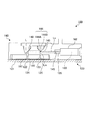
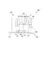
- FIG. 1 is a cross-sectional view of the optical module according to the first embodiment.
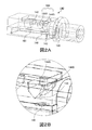
- 2A and 2B are perspective views showing the configuration of the optical receptacle according to the first embodiment.
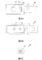
- 3A to 3C are diagrams showing the configuration of the optical receptacle according to the first embodiment.
- FIG. 4 is a partially enlarged cross-sectional view showing the configuration of the optical receptacle according to the first embodiment.
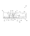
- FIG. 5 is a cross-sectional view of the optical module for comparison.
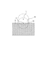
- FIG. 6 is a cross-sectional view showing the positional relationship between the light incident on the first optical surface and the transmission portion in the cross section taken along the line BB in FIG.
- FIG. 7 is a partial enlarged cross-sectional view of the vicinity of the light separation unit of FIG. FIG.
- FIG. 8 is a cross-sectional view showing the positional relationship between the light incident on the first optical surface and the first transmitting portion and the second transmitting portion in the cross section taken along the line BB in FIG.
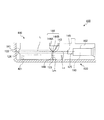
- FIG. 9 is a cross-sectional view of the optical module according to the second embodiment.
- 10A to 10C are diagrams showing the configuration of an optical receptacle according to Embodiment 2.
- FIG. 11 is a partial enlarged cross-sectional view showing the configuration of the optical receptacle according to the second embodiment.
- FIG. 12 is a cross-sectional view of the optical module according to the third embodiment.
- 13A and 13B are perspective views showing the configuration of the optical receptacle according to the third embodiment.
- 14A to 14C are diagrams showing the configuration of the optical receptacle according to the third embodiment.
- FIG. 15 is a cross-sectional view of an optical module according to a modification.
- FIG. 1 is a cross-sectional view of the optical module 100 according to the first embodiment.
- the optical path of the optical module 100 is shown in FIG. In FIG. 1, hatching to a cross section of the optical receptacle 140 is omitted to show an optical path in the optical receptacle 140.
- the optical module 100 includes a substrate-mounted photoelectric conversion device 120 including a light emitting element 122, and an optical receptacle 140.
- the optical module 100 is an optical module for transmission, and the optical transmitter 160 is coupled to the optical receptacle 140 via the ferrule 162 (hereinafter also referred to as connection) and used.
- the type of the light transmitter 160 is not particularly limited, and includes an optical fiber, an optical waveguide, and the like.
- the light transmitting body 160 is an optical fiber.
- the optical fiber may be a single mode system or a multimode system.
- the number of light transmitters 160 is not particularly limited. In the present embodiment, the number of light transmission bodies 160 is one.
- the photoelectric conversion device 120 includes a substrate 121, one light emitting element 122, and one detection element 123.
- the substrate 121 is, for example, a glass composite substrate, a glass epoxy substrate, a flexible sill substrate, or the like.
- the light emitting element 122 and the detection element 123 are disposed on the substrate 121.
- the light emitting element 122 is disposed on the substrate 121, and emits laser light in a direction perpendicular to the installation portion of the substrate 121 on which the light emitting element 122 is disposed.
- the number of light emitting elements 122 is not particularly limited. In the present embodiment, the number of light emitting elements 122 is one. Further, the position of the light emitting element 122 is also not particularly limited.
- the light emitting element 122 is, for example, a vertical cavity surface emitting laser (VCSEL).
- the detection element 123 receives monitor light Lm for monitoring the output (for example, the intensity and the amount of light) of the emitted light L emitted from the light emitting element 122.
- the detection element 123 is, for example, a photodetector.
- the number of detection elements 123 is not particularly limited. In the present embodiment, the number of detection elements 123 is one. Further, from the viewpoint of preventing the reflected light from the detection element 123 from returning into the optical receptacle 140, the optical axis of the monitor light Lm incident on the detection element 123 is inclined with respect to the detection surface 126 of the detection element 123. May be
- the optical receptacle 140 is disposed on the substrate 121 of the photoelectric conversion device 120.
- the optical receptacle 140 optically couples the light emitting surface 124 of the light emitting element 122 and the end face 125 of the light transmitting member 160 in a state where the optical receptacle 140 is disposed between the photoelectric conversion device 120 and the light transmitting member 160 Say)
- the configuration of the optical receptacle 140 will be described in detail.
- FIGS. 2A and 2B, FIGS. 3A to 3C, and FIG. 4 are diagrams showing the configuration of the optical receptacle 140 according to the present embodiment.
- FIG. 2A is a perspective view of the optical receptacle 140
- FIG. 2B is a partially enlarged perspective view of FIG. 2A.
- 3A is a plan view of the optical receptacle 140
- FIG. 3B is a bottom view
- FIG. 3C is a front view.
- FIG. 4 is a partially enlarged cross-sectional view showing the configuration of the optical receptacle according to the present embodiment.
- the optical receptacle 140 has translucency, and uses a part of the outgoing light L emitted from the light emitting surface 124 of the light emitting element 122 as the signal light Ls. It is emitted toward the end face 125 of the light transmission body 160, and the other part is emitted toward the detection element 123 as the monitor light Lm.
- the optical receptacle 140 has a first optical surface 141, a reflective surface 142, a first transmitting portion 143, a light separating portion 144, a second optical surface 145, and a third optical surface 146.
- the light separating unit 144 has a reflecting unit 144A and a second transmitting unit 144B.
- the number of the first optical surface 141, the first transmitting portion 143, the second transmitting portion 144B, the second optical surface 145, and the third optical surface 146 is one.
- the optical receptacle 140 is formed using a material having transparency to light of a wavelength used for optical communication. Examples of such materials include transparent resins such as polyetherimide (PEI) and cyclic olefin resins. Also, for example, the optical receptacle 140 is manufactured by injection molding.
- PEI polyetherimide
- cyclic olefin resins such as polyetherimide (PEI)
- the optical receptacle 140 is manufactured by injection molding.
- the first optical surface 141 is an optical surface that refracts the emitted light L emitted from the light emitting element 122 and makes the light enter the inside of the optical receptacle 140.
- the first optical surface 141 can convert the outgoing light L emitted from the light emitting element 122 into collimated light, convergent light, or diffused light.
- the first optical surface 141 converts the outgoing light L emitted from the light emitting element 122 into collimated light.
- the shape of the first optical surface 141 is a convex lens surface convex toward the light emitting element 122.
- the planar view shape of the 1st optical surface 141 is circular shape.
- the central axis of the first optical surface 141 is preferably perpendicular to the light emitting surface 124 of the light emitting element 121. In addition, it is preferable that the central axis of the first optical surface 141 be coincident with the optical axis of the emitted light L emitted from the light emitting element 122.
- the reflecting surface 142 is an inclined surface formed on the top surface side of the optical receptacle 140, and the optical path between the first optical surface 141 and the first transmitting portion 143 and the first optical surface 141 and the light separating portion 144. Located on the light path between The reflective surface 142 reflects the light incident on the first optical surface 141 (the emitted light L emitted from the light emitting element 122) toward the first transmitting portion 143 and the light separating portion 144. The reflective surface 142 is inclined so as to approach the light transmitting body 160 as it goes from the bottom surface of the optical receptacle 140 to the top surface.
- the inclination angle of the reflective surface 142 is 45 ° with respect to the optical axis of the outgoing light L incident on the first optical surface 141.
- the outgoing light L incident on the first optical surface 141 is internally incident on the reflecting surface 142 at an incident angle larger than the critical angle.
- the reflecting surface 142 totally reflects the incident outgoing light L in the direction along the surface of the substrate 121.
- the first transmission portion 143 is a region that transmits part of the light incident on the first optical surface 141 as the signal light Ls directed to the end surface 125 of the light transmission body 160.
- the first transmitting portion 143 is disposed in contact with the second transmitting portion 144B of the light separating portion 144.
- the light separation unit 144 generates monitor light Lm for directing another portion (preferably, the remaining portion) of the light incident on the first optical surface 141 to the third optical surface 146 (or the detection element 123), and the second optical surface 145. (Or the end face 125 of the light transmitter 160) and the signal light Ls.
- the light separation unit 144 has a reflection unit 144A and a second transmission unit 144B.
- the reflector 144A is disposed on the top surface side of the optical receptacle 140.
- the reflecting portion 144A is an inclined surface with respect to the optical axis of the light incident on the first optical surface 141, and reflects part of the other part of the light incident on the light separating portion 144 toward the third optical surface 146.
- the reflecting portion 144A is an inclined surface which is inclined so as to approach the second optical surface 145 (the light transmitting body 160) as it goes from the top surface to the bottom surface of the optical receptacle 140.
- the inclination angle of the inclined surface is 45 ° with respect to the optical axis of the light incident on the first optical surface 141.
- the second transmission part 144B is disposed adjacent to the reflection part 144A, and transmits a part of the other part of the light incident on the light separation part 144 (light other than the light reflected by the reflection part 144A) Transmit as light Ls.
- the second transmission part 144 ⁇ / b> B is preferably in contact with the first transmission part 143.
- the boundary portion 148 between the first transmission portion 143 and the light separation portion 144 is located in the vicinity of the optical axis of the light incident on the first optical surface 141 (described later) See Figure 8).
- the optical axis of light incident on the first optical surface 141 and emitted on the second optical surface 145 is taken as the central axis C, and the optical surface of the larger one of the first optical surface 141 and the second optical surface 145 from the central axis C
- the optical effective area A is a cylindrical area whose outer edge is a surface separated from the central axis C by the same distance as the radius of the second optical surface 145.
- the emitted light from the light emitting element 122 has a higher intensity as it gets closer to the optical axis. Therefore, if the position in the height direction of the light separation unit 144 is slightly deviated in the vicinity of the optical axis, the spectral ratio of the monitor light Lm and the signal light Ls is likely to fluctuate relatively large.
- the cross section perpendicular to the optical axis of the light L incident on the first optical surface 141 (the light reflected on the reflective surface 142
- the second transmission portion 144B includes at least the vicinity of the optical axis of the light L incident on the first optical surface 141 (so as to surround the vicinity of the optical axis of the light L) Preferably).
- the cross-sectional shape of the second transmission part 144B is not particularly limited, and may be an arc or a polygon (triangle, rectangle Etc.).
- the arcuate shape is a shape in which both ends of an arc or an elliptic arc are connected by a straight line, and examples thereof include a semicircular shape and the like.
- the light source has a semicircular shape centered on the intersection of the optical axis of the light L incident on the first optical surface 141 and the boundary portion 148 (see FIGS. 2B and 8).
- the cross sectional area of the second transmission part 144B is smaller than the cross sectional area of the optically effective area A.
- the cross-sectional area of the second transmission part 144B is preferably 18 to 36%, and more preferably 18 to 29%, of the cross-sectional area of the optical effective area A.
- the height direction is a direction connecting the bottom surface and the top surface of the optical receptacle 140, and is a direction perpendicular to the optical axis of the light transmitted through the first transmission portion 143 or the second transmission portion 144B. .
- the second transmission part 144B is disposed such that the signal light Ls transmitted therethrough is emitted to the outside of the optical receptacle 140 for the first time by the second optical surface 145 (see FIG. 1). That is, the second transmission part 144B transmits the light transmitted through the second transmission part 144B, which is disposed on the optical path between the second transmission part 144B and the second optical surface 145, to the outside of the optical receptacle 140. It does not have a face.
- a part of the light L incident on the first optical surface 141 is transmitted through the first transmission portion 143 and becomes the signal light Ls directed to the end face 125 of the light transmission body 160.
- the other part (preferably the remaining part) of the light incident on the first optical surface 141 is incident on the light separation part 144, and a part thereof is reflected on the reflection part 144A and becomes monitor light Lm directed to the detection element
- a part of the light other than the light reflected by the reflection part 144A passes through the second transmission part 144B and travels to the end face 125 of the light transmission body 160. It becomes signal light Ls.
- the light amount ratio between the signal light Ls and the monitor light Lm is to obtain the monitor light Lm capable of monitoring the intensity and the light amount of the light L emitted from the light emitting element 122 while obtaining the signal light Ls having a desired light amount. If possible, it is not particularly limited.
- the signal light Ls is the sum of the signal light passing through the first transmitting portion 143 and the signal light passing through the second transmitting portion 144B.
- the second optical surface 145 is an optical surface that emits the signal light Ls transmitted through the first transmission portion 143 and the signal light Ls separated by the light separation portion 144 toward the end face 125 of the light transmission body 160. .
- the second optical surface 145 is disposed on the front of the optical receptacle 140 so as to face the end face 125 of the light transmission body 160.
- the shape of the second optical surface 145 is a convex lens surface convex toward the end surface 125 of the light transmission body 160.
- the third optical surface 146 is disposed on the bottom surface side of the optical receptacle 140 so as to face the detection element 123.
- the third optical surface 146 is a convex lens surface that is convex toward the detection element 123.
- the third optical surface 146 converges the monitor light Lm separated by the reflection part 144A of the light separation part 144 and emits it toward the detection element 123.
- the monitor light Lm can be efficiently coupled to the detection element 123.
- the central axis of the third optical surface 146 is preferably perpendicular to the light receiving surface (substrate 121) of the detection element 123.
- FIG. 5 is a cross-sectional view showing the configuration of the optical module 10 for comparison.
- the optical module 10 for comparison is configured in the same manner as the optical module 100 according to the present embodiment except that the optical receptacle 14 does not have the second transmission portion.
- FIG. 6 is a cross-sectional view showing the positional relationship between the light L incident on the first optical surface 41 and the first transmitting portion 43 in the cross section taken along the line BB in FIG.
- FIG. 7 is a partial enlarged cross-sectional view in the vicinity of the light separation unit 144 in FIG.
- FIG. 8 is a cross-sectional view showing the positional relationship between the light L incident on the first optical surface 141 and the first transmitting portion 143 and the second transmitting portion 144B in the cross section taken along the line BB in FIG.
- the outgoing light L emitted from the light emitting element 122 is incident on the optical receptacle 14 at the first optical surface 41.
- the light incident on the first optical surface 41 is reflected on the reflection surface 42, and then a part thereof is transmitted through the first transmission part 43 and becomes signal light Ls directed to the light transmission body 160, and the other part (preferably Is reflected by the reflection section 44A to become monitor light Lm directed to the detection element 123.
- the signal light Ls that passes through the first transmission portion 43 and travels to the light transmission body 160 is emitted from the second optical surface 45 and reaches the end surface 125 of the light transmission body 160.
- the monitor light Lm traveling toward the detection element 123 is emitted from the third optical surface 46 and reaches the detection element 123.
- the position of light incident on the first optical surface 141 is, for example, the first transmitting portion due to the positional deviation of the reflecting portion 44A in the optical receptacle 14.
- the intensity of the signal light Ls decreases significantly.
- Cheap That is, the fluctuation of the spectral ratio of the signal light Ls transmitted through the first transmission portion 43 and the monitor light Lm reflected by the reflection portion 44A is relatively large.
- the outgoing light L emitted from the light emitting element 122 is incident on the optical receptacle 140 at the first optical surface 141.
- Ru The light incident on the first optical surface 141 is reflected on the reflection surface 142, and a part thereof is transmitted through the first transmission part 143 to become signal light Ls directed to the light transmission body 160, and the other part ( Preferably, the remaining portion is incident on the light separation unit 144.
- a part of the light incident on the light separation part 144 is reflected by the reflection part 144A to become monitor light Lm directed to the detection element 123, and a part of light other than the light reflected by the reflection part 144A (preferably the reflection part).
- the light other than the light reflected by 144A is transmitted through the second transmission part 144B and becomes the signal light Ls traveling toward the light transmission body 160.
- the signal light Ls transmitted through the first transmission portion 143 and the signal light Ls transmitted through the second transmission portion 144 B are emitted from the second optical surface 145 and reach the end surface 125 of the light transmission body 160.
- monitor light Lm traveling toward the detection element 123 is emitted from the third optical surface 146 and reaches the detection element 123.
- the position of light incident on the first optical surface 141 due to the positional deviation of the light separation unit 144 in the optical receptacle 140 is Even when shifted upward with respect to the first transmission portion 143 (see the arrow), light in the vicinity of the center of high intensity passes through the second transmission portion 144B and travels to the second optical surface 145, so the intensity of the signal light Ls There is little decrease. That is, the fluctuation of the spectral ratio of the signal light Ls and the monitor light Lm can be reduced.
- the position in the height direction of the light separation unit 144 is shifted every 0.002 mm from the reference position (0 mm) upward to 0.02 mm.
- the ratio (%) of the monitor light Lm to the emitted light L emitted from the light emitting element 122 was simulated using analysis software.
- the reference position is a position where the boundary portion 148 (see FIG. 8) of the first transmission portion 143 and the second transmission portion 144B overlaps the optical axis of the light L incident on the first optical surface 141.
- the optical module 10 (see FIG. 5) using the comparative optical receptacle configured similarly to the optical module 100 according to the present embodiment except that the second transmission part is not provided for comparison is also the same. It was simulated.
- a vertical cavity surface emitting laser having a numerical aperture (NA: numerical aperture) of 0.25 and an emission diameter of ⁇ 8 ⁇ m was used as the light emitting element 122.
- the simulation results are shown in Table 1.
- the position in the height direction of the light separation portion 144 is used in order to set the target (for example, 5 to 14%) of the target monitor light. It is understood that it is preferable that the value is in the range of 0 to 0.018 mm.
- the position of the light separating portion 44 in the height direction is 0 to 0.014 mm in order to achieve the target monitoring light ratio (for example, 5 to 14%) It must be understood that it must be in the range of
- the range of the position in the height direction of the light separation section 144 which is permitted to achieve the target monitor light ratio is wider in the optical module according to the present embodiment, that is, the optical receptacle It can be understood that the positional accuracy of the light separating unit 144 can be relaxed.
- the optical module 100 further includes not only the first transmitting portion 143 but also the second transmitting portion 144B.
- the optical module 100 further includes not only the first transmitting portion 143 but also the second transmitting portion 144B.
- the optical module 200 according to the second embodiment differs from the optical module 100 according to the first embodiment in the configuration of the optical receptacle 240.
- the optical receptacle 240 according to the present embodiment differs from the optical receptacle 140 according to the first embodiment in that the shape of the second transmitting portion 244B is different and the fourth optical surface 147 is further included. Therefore, only the second transmitting portion 244B and the fourth optical surface 147 will be described, and the same configuration as that of the first embodiment will be assigned the same reference numerals and descriptions thereof will be omitted.
- FIG. 9 is a cross-sectional view of the optical module 200 according to the second embodiment.
- the optical path of the optical module 200 is shown in FIG. In FIG. 9, hatching to the cross section of the optical receptacle 240 is omitted to show the optical path in the optical receptacle 240.
- the optical module 200 has a substrate mounting type photoelectric conversion device 120 including the light emitting element 122, and an optical receptacle 240.
- FIG. 10A to 10C and 11 show the configuration of the optical receptacle 240 according to the present embodiment.
- 10A is a plan view of the optical receptacle 240
- FIG. 10B is a bottom view
- FIG. 10C is a front view.
- FIG. 11 is a partially enlarged cross-sectional view showing the configuration of the optical receptacle 240 according to the present embodiment.
- the optical receptacle 240 differs in the shape of the second transmission part 244B of the light separation part 244, and the light separation part 244 (the transmission surface 244C of the light separation part 244)
- the optical receptacle 140 according to the first embodiment shown in FIG. 1 is the same as the optical receptacle 140 according to the first embodiment shown in FIG. 1 except that the fourth optical surface 147 is disposed on the optical path between the two optical surfaces 145.
- the second transmitting unit 244B is disposed on the optical path between the first optical surface 141 and the second optical surface 145, and is a transmitting surface perpendicular to the optical axis of the signal light Ls separated by the light separating unit 244. It has 244C.
- the perpendicular plane herein refers to a plane of ⁇ 5 ° or less, preferably a plane of 0 ° with respect to a line perpendicular to the optical axis of the signal light Ls separated by the light separation unit 244.
- the transmission surface 244 C emits the signal light Ls separated by the light separation unit 244 to the outside of the optical receptacle 240.
- the fourth optical surface 147 is a surface formed on the top surface side of the optical receptacle 240 and perpendicular to the optical axis of the signal light Ls separated by the light separation unit 244.
- the perpendicular plane refers to a plane of ⁇ 5 ° or less, preferably 0 °, with respect to a line perpendicular to the optical axis of the signal light Ls separated by the light separation unit 244.
- the fourth optical surface 147 is disposed on the light path between the transmission surface 244C and the second optical surface 145.
- the fourth optical surface 147 separates the signal light Ls separated to the outside of the optical receptacle 240 by the light separating section 244 and re-enters the inside of the optical receptacle 240. Accordingly, the signal light Ls traveling toward the end face 125 of the light transmission body 160 can be re-entered into the optical receptacle 140 without being refracted.
- a part of the light incident on the light separation part 244 is reflected by the reflection part 144A to become monitor light Lm directed to the detection element 123, and a part of light other than the light reflected by the reflection part 144A (preferably the reflection part).
- the light other than the light reflected by 144A is transmitted through the second transmission portion 244B, and is emitted from the transmission surface 244C to the outside of the optical receptacle 240 as the signal light Ls that travels to the light transmission body 160.
- the signal light Ls emitted from the transmission surface 244 ⁇ / b> C reenters the inside of the optical receptacle 240 at the fourth optical surface 147. Then, the signal light Ls incident again on the fourth optical surface 147 and the signal light Ls transmitted through the first transmission portion 143 are emitted from the second optical surface 145 and reach the end surface 125 of the light transmission body 160.
- the position of light incident on the first optical surface 141 is, for example, due to the positional deviation of the light separation unit 244 in the optical receptacle 240, as in the first embodiment. Even if the light is shifted upward with respect to the first transmitting portion 143, light in the vicinity of the center of high intensity transmits the second transmitting portion 244B and travels to the second optical surface 145, so the decrease in the intensity of the signal light Ls is small. That is, the fluctuation of the spectral ratio of the signal light Ls and the monitor light Lm can be reduced.
- the optical module 300 according to the third embodiment differs from the optical module 100 according to the first embodiment in that the optical receptacle 340 is of a lens array type and is configured to be compatible with multi-channel light transmission.
- the same components as in the first embodiment will be assigned the same reference numerals and descriptions thereof will be omitted.
- FIG. 12 is a cross-sectional view of the optical module 300 according to the third embodiment. As shown in FIG. 12, the optical module 300 has a substrate mounting type photoelectric conversion device 320 including the light emitting element 122, and an optical receptacle 340.
- the optical transmission body 160 is attached to the optical receptacle 340 via a known attachment means in a state of being accommodated in the multi-core collective type connector.
- four light transmitters 160 are arranged in a line at regular intervals.
- the light transmitters 160 may be arranged in two or more rows.
- the photoelectric conversion device 320 includes a substrate 121, a plurality of light emitting elements 122, and a plurality of detecting elements 123.
- the number of light emitting elements 122 and detection elements 123 is not particularly limited as long as it is plural. In the present embodiment, the number of light emitting elements 122 and detecting elements 123 is four.
- the four light emitting elements 123 are arranged in a line on the substrate 121.
- the four light emitting elements 122 are arranged in a line in the direction perpendicular to the paper surface.
- the four light emitting elements 122 are arranged at regular intervals along the arrangement direction of the light transmitters 160.
- the four detection elements 123 are disposed on the substrate 121.
- the four detection elements 123 are arranged in one row at regular intervals corresponding to the four light emitting elements 122.
- FIGS. 14A to 14C are diagrams showing the configuration of the optical receptacle 340 according to the present embodiment.
- FIG. 13A is a perspective view of the optical receptacle 340 as viewed from the front side
- FIG. 13B is a perspective view of the optical receptacle 340 as viewed from the back side.
- 14A is a plan view of the optical receptacle 340
- FIG. 14B is a bottom view
- FIG. 14C is a front view.
- the optical receptacle 340 includes a plurality of first optical surfaces 141, a reflection surface 142, a plurality of first transmission parts 143, and a plurality of reflection parts. 144A, a plurality of second transmitting portions 144B, a plurality of second optical surfaces 145, and a plurality of third optical surfaces 146.
- the number of the first optical surface 141, the second optical surface 145, the first transmitting portion 143, the second transmitting portion 144B, and the third optical surface 146 is four.
- the optical module 300 according to the present embodiment can cope with multichannel optical transmission with monitoring.
- the optical receptacles 140, 240, and 340 each have the reflecting surface 142.
- the present invention is not limited to this.
- FIG. 15 is a cross-sectional view of an optical module 400 according to a modification.
- the optical module 400 has a photoelectric conversion device 420 including the light emitting element 122 and an optical receptacle 440.
- the optical receptacle 440 may be configured the same as the optical receptacle 140 of FIG. 1 except that the first optical surface 141 is disposed on the back surface of the optical receptacle 440 and does not have the reflective surface 142.
- the substrate 421 of the photoelectric conversion device 420 is disposed such that the light emitting element 122 faces the first optical surface 141 of the optical receptacle 440 and the detection element 123 faces the third optical surface 146.
- the reflecting surface 142 and the reflecting portion 144A are not in contact with each other on the top surface side of the optical receptacles 140, 240, and 340.
- the reflective surface 142 and the reflective portion 144A may be disposed in contact with each other.
- the first optical surface 141, the second optical surface 145, and the third optical surface 146 all have convex lens surfaces.
- the present invention is not limited to this, and may be, for example, a plane.
- the planar view shape of the 1st optical surface 141, the 2nd optical surface 145, and the 3rd optical surface 146 showed the example which is circular all, it is not limited to this.
- the optical module 300 is used as an optical module for transmission
- An example is shown, but not limited to this.
- all four first optical surfaces 141 may be used as the first optical surface 141 for reception (the optical module 300 may be used as an optical module for reception), or either the right side or the left side may be used.
- One of the two first optical surfaces 141 may be used as the first optical surface 141 for reception (the optical module 300 may be used as an optical module serving both transmission and reception).
- the present invention is not limited thereto, and the light separating portion 144 It may be a plane perpendicular to the optical axis of the signal light Ls.
- the perpendicular plane is a plane of ⁇ 5 ° or less, preferably 0 °, with respect to a line perpendicular to the optical axis of the signal light Ls separated by the light separation unit 144.
- optical receptacle and the optical module according to the present invention are useful for optical communication using an optical transmitter.
- Optical module 120 100, 200, 300, 400 Optical module 120, 320, 420 Photoelectric conversion device 121, 421 Substrate 122 Light emitting element 123 Detection element 124 Light emitting surface 125 End surface 140, 240, 340, 440 Optical receptacle 141 First optical surface 142 Reflective surface 143 First transmitting portion 144, 244 Light separating portion 144A Reflecting portion 144B, 244B Second transmitting portion 145 Second optical surface 146 Third optical surface 147 Fourth optical surface 148 Boundary portion 160 Light transmission body 162 Ferrule 244C Transmission surface L Emitting light Lm monitor light Ls signal light A optical effective area Rmax radius
Landscapes
- Physics & Mathematics (AREA)
- General Physics & Mathematics (AREA)
- Optics & Photonics (AREA)
- Condensed Matter Physics & Semiconductors (AREA)
- Electromagnetism (AREA)
- Optical Couplings Of Light Guides (AREA)
- Semiconductor Lasers (AREA)
Abstract
Selon la présente invention, un réceptacle optique comprend : une première surface optique recevant une lumière émise par un élément électroluminescent ; une première partie de transmission permettant de transmettre une partie de la lumière reçue par la première surface optique en tant que lumière de signal ; une unité de séparation de lumière permettant de séparer l'autre partie de la lumière reçue par la première surface optique en lumière de surveillance et en lumière de signal ; une deuxième surface optique permettant d'émettre la lumière de signal transmise à travers la première partie de transmission et la lumière de signal séparée par l'unité de séparation de lumière vers la surface d'extrémité d'un corps de transmission optique ; et une troisième surface optique permettant d'émettre la lumière de surveillance vers un élément de détection. L'unité de séparation de lumière comprend une partie réfléchissante et une deuxième partie de transmission. Étant donné que l'axe optique de la lumière qui est incidente sur la première surface optique et qui sort de la deuxième surface optique est défini en tant qu'axe central et qu'une zone, qui possède une surface périphérique externe à la même distance de l'axe central que le rayon de la première surface optique ou de la deuxième surface optique, selon la valeur qui est plus grande, est définie en tant que zone efficace optique, la première partie de transmission et la deuxième partie de transmission sont situées à l'intérieur de la zone efficace optique.
Priority Applications (2)
| Application Number | Priority Date | Filing Date | Title |
|---|---|---|---|
| CN201880046652.5A CN110892303B (zh) | 2017-07-14 | 2018-07-13 | 光插座及光模块 |
| US16/630,862 US10976510B2 (en) | 2017-07-14 | 2018-07-13 | Optical receptacle and optical module |
Applications Claiming Priority (2)
| Application Number | Priority Date | Filing Date | Title |
|---|---|---|---|
| JP2017138328A JP6943660B2 (ja) | 2017-07-14 | 2017-07-14 | 光レセプタクルおよび光モジュール |
| JP2017-138328 | 2017-07-14 |
Publications (1)
| Publication Number | Publication Date |
|---|---|
| WO2019013313A1 true WO2019013313A1 (fr) | 2019-01-17 |
Family
ID=65002448
Family Applications (1)
| Application Number | Title | Priority Date | Filing Date |
|---|---|---|---|
| PCT/JP2018/026422 Ceased WO2019013313A1 (fr) | 2017-07-14 | 2018-07-13 | Réceptacle optique et module optique |
Country Status (5)
| Country | Link |
|---|---|
| US (1) | US10976510B2 (fr) |
| JP (1) | JP6943660B2 (fr) |
| CN (1) | CN110892303B (fr) |
| TW (1) | TW201908791A (fr) |
| WO (1) | WO2019013313A1 (fr) |
Cited By (3)
| Publication number | Priority date | Publication date | Assignee | Title |
|---|---|---|---|---|
| CN110794529A (zh) * | 2020-01-06 | 2020-02-14 | 成都新易盛通信技术股份有限公司 | 一种光组件及其系统 |
| US10976510B2 (en) | 2017-07-14 | 2021-04-13 | Enplas Corporation | Optical receptacle and optical module |
| US11759544B2 (en) | 2018-05-25 | 2023-09-19 | Locus Solutions Ipco, Llc | Therapeutic compositions for enhanced healing of wounds and scars |
Families Citing this family (6)
| Publication number | Priority date | Publication date | Assignee | Title |
|---|---|---|---|---|
| JP7125309B2 (ja) * | 2018-09-03 | 2022-08-24 | 株式会社エンプラス | 光モジュール |
| CN111665599A (zh) * | 2019-03-08 | 2020-09-15 | 苏州旭创科技有限公司 | 光模块 |
| WO2021103958A1 (fr) * | 2019-11-25 | 2021-06-03 | 青岛海信宽带多媒体技术有限公司 | Module optique |
| US11493707B2 (en) * | 2021-03-31 | 2022-11-08 | Enplas Corporation | Optical receptacle and optical module |
| CN114879324B (zh) | 2022-06-24 | 2023-08-08 | 青岛海信宽带多媒体技术有限公司 | 光模块 |
| CN114994839B (zh) * | 2022-06-24 | 2023-08-08 | 青岛海信宽带多媒体技术有限公司 | 光模块 |
Citations (7)
| Publication number | Priority date | Publication date | Assignee | Title |
|---|---|---|---|---|
| JPS62237409A (ja) * | 1986-04-09 | 1987-10-17 | Seiko Instr & Electronics Ltd | 発光モジユ−ル |
| JP2012163903A (ja) * | 2011-02-09 | 2012-08-30 | Furukawa Electric Co Ltd:The | 光通信モジュール及び光結合部材 |
| JP2013024918A (ja) * | 2011-07-15 | 2013-02-04 | Enplas Corp | 光レセプタクルおよびこれを備えた光モジュール |
| JP2013061587A (ja) * | 2011-09-15 | 2013-04-04 | Alps Electric Co Ltd | ビームスプリッタ及びそれを用いた光通信モジュール |
| WO2016104302A1 (fr) * | 2014-12-25 | 2016-06-30 | 株式会社エンプラス | Procédé de mesure et réceptacle optique |
| WO2017057035A1 (fr) * | 2015-10-02 | 2017-04-06 | 株式会社エンプラス | Récipient optique et module optique |
| US20170168250A1 (en) * | 2015-12-15 | 2017-06-15 | Huawei Technologies Co., Ltd. | Integrally formed coupling module |
Family Cites Families (34)
| Publication number | Priority date | Publication date | Assignee | Title |
|---|---|---|---|---|
| WO1998014818A1 (fr) * | 1996-09-30 | 1998-04-09 | Siemens Aktiengesellschaft | Procede pour produire un corps façonne separateur de faisceaux et utilisation de ce dernier dans un module optoelectronique |
| US6219470B1 (en) * | 1999-09-23 | 2001-04-17 | Xiang Zheng Tu | Wavelength division multiplexing transmitter and receiver module |
| DE19947889C2 (de) * | 1999-10-05 | 2003-03-06 | Infineon Technologies Ag | Optoelektronisches, bidirektionales Sende- und Empfangsmodul in Leadframe-Technik |
| US6571033B2 (en) * | 2001-09-28 | 2003-05-27 | Corning Incorporated | Optical signal device |
| US6636540B2 (en) * | 2001-10-30 | 2003-10-21 | Agilent Technologies, Inc. | Optical turn for monitoring light from a laser |
| US6939058B2 (en) * | 2002-02-12 | 2005-09-06 | Microalign Technologies, Inc. | Optical module for high-speed bidirectional transceiver |
| JP2003255195A (ja) * | 2002-02-27 | 2003-09-10 | Sumitomo Electric Ind Ltd | 波長多重コネクタ、光通信装置および光通信システム |
| JP3896905B2 (ja) * | 2002-06-18 | 2007-03-22 | 住友電気工業株式会社 | 光通信装置 |
| US6963683B2 (en) * | 2002-09-30 | 2005-11-08 | Intel Corporation | System and method for a packaging a monitor photodiode with a laser in an optical subassembly |
| US6888988B2 (en) * | 2003-03-14 | 2005-05-03 | Agilent Technologies, Inc. | Small form factor all-polymer optical device with integrated dual beam path based on total internal reflection optical turn |
| US6895147B2 (en) * | 2003-06-26 | 2005-05-17 | Intel Corporation | Laser power monitoring tap |
| JP2005234052A (ja) * | 2004-02-17 | 2005-09-02 | Hamamatsu Photonics Kk | 光送受信モジュール |
| KR100802199B1 (ko) * | 2006-05-25 | 2008-03-17 | 정경희 | 광모듈 및 그 제조방법 |
| JP2008225339A (ja) * | 2007-03-15 | 2008-09-25 | Hitachi Cable Ltd | 光学系接続構造、光学部材及び光伝送モジュール |
| US7991251B2 (en) * | 2008-07-02 | 2011-08-02 | Hitachi, Ltd. | Optical module mounted with WDM filter |
| CN102667565B (zh) * | 2009-12-22 | 2015-05-13 | 恩普乐股份有限公司 | 透镜阵列以及具备该透镜阵列的光学模块 |
| JP5702596B2 (ja) * | 2010-10-28 | 2015-04-15 | 株式会社エンプラス | レンズアレイおよびこれを備えた光モジュール |
| JP5896098B2 (ja) * | 2010-12-09 | 2016-03-30 | 株式会社エンプラス | レンズアレイ |
| US8933391B2 (en) * | 2011-02-01 | 2015-01-13 | SiFotonics Technologies Co, Ltd. | Monolithic optical coupling module based on total internal reflection surfaces |
| WO2012169587A1 (fr) * | 2011-06-09 | 2012-12-13 | 株式会社エンプラス | Réseau de lentilles, et module optique équipé de celui-ci |
| JP6089354B2 (ja) * | 2011-10-25 | 2017-03-08 | 株式会社エンプラス | レンズアレイおよびその製造方法 |
| JP6134934B2 (ja) * | 2011-12-02 | 2017-05-31 | 株式会社エンプラス | 光レセプタクルおよびこれを備えた光モジュール |
| JP5896136B2 (ja) * | 2012-03-05 | 2016-03-30 | 株式会社エンプラス | 光レセプタクルおよびこれを備えた光モジュール |
| JP6011958B2 (ja) * | 2012-03-28 | 2016-10-25 | 株式会社エンプラス | 光レセプタクルおよびこれを備えた光モジュール |
| JP6205194B2 (ja) * | 2013-07-08 | 2017-09-27 | 株式会社エンプラス | 光レセプタクルおよび光モジュール |
| JP6359848B2 (ja) * | 2014-03-18 | 2018-07-18 | 株式会社エンプラス | 光レセプタクルおよびこれを備えた光モジュール |
| JP6461509B2 (ja) * | 2014-08-04 | 2019-01-30 | 株式会社エンプラス | 光レセプタクルおよび光モジュール |
| JP6532236B2 (ja) * | 2015-01-28 | 2019-06-19 | 株式会社エンプラス | 光レセプタクルおよび光モジュール |
| US9692522B2 (en) * | 2015-04-15 | 2017-06-27 | Cisco Technology, Inc. | Multi-channel optical receiver or transmitter with a ball lens |
| CN106291834A (zh) * | 2015-05-22 | 2017-01-04 | 鸿富锦精密工业(深圳)有限公司 | 光学通讯装置 |
| JP6676412B2 (ja) * | 2016-03-03 | 2020-04-08 | 株式会社エンプラス | 光レセプタクル、光モジュールおよび光モジュールの製造方法 |
| JP2017161578A (ja) * | 2016-03-07 | 2017-09-14 | 株式会社エンプラス | 光レセプタクルおよび光モジュール |
| JP6943660B2 (ja) | 2017-07-14 | 2021-10-06 | 株式会社エンプラス | 光レセプタクルおよび光モジュール |
| JP6959807B2 (ja) * | 2017-09-11 | 2021-11-05 | 株式会社エンプラス | 光レセプタクルおよび光モジュール |
-
2017
- 2017-07-14 JP JP2017138328A patent/JP6943660B2/ja active Active
-
2018
- 2018-07-13 CN CN201880046652.5A patent/CN110892303B/zh active Active
- 2018-07-13 WO PCT/JP2018/026422 patent/WO2019013313A1/fr not_active Ceased
- 2018-07-13 US US16/630,862 patent/US10976510B2/en active Active
- 2018-07-13 TW TW107124263A patent/TW201908791A/zh unknown
Patent Citations (7)
| Publication number | Priority date | Publication date | Assignee | Title |
|---|---|---|---|---|
| JPS62237409A (ja) * | 1986-04-09 | 1987-10-17 | Seiko Instr & Electronics Ltd | 発光モジユ−ル |
| JP2012163903A (ja) * | 2011-02-09 | 2012-08-30 | Furukawa Electric Co Ltd:The | 光通信モジュール及び光結合部材 |
| JP2013024918A (ja) * | 2011-07-15 | 2013-02-04 | Enplas Corp | 光レセプタクルおよびこれを備えた光モジュール |
| JP2013061587A (ja) * | 2011-09-15 | 2013-04-04 | Alps Electric Co Ltd | ビームスプリッタ及びそれを用いた光通信モジュール |
| WO2016104302A1 (fr) * | 2014-12-25 | 2016-06-30 | 株式会社エンプラス | Procédé de mesure et réceptacle optique |
| WO2017057035A1 (fr) * | 2015-10-02 | 2017-04-06 | 株式会社エンプラス | Récipient optique et module optique |
| US20170168250A1 (en) * | 2015-12-15 | 2017-06-15 | Huawei Technologies Co., Ltd. | Integrally formed coupling module |
Cited By (3)
| Publication number | Priority date | Publication date | Assignee | Title |
|---|---|---|---|---|
| US10976510B2 (en) | 2017-07-14 | 2021-04-13 | Enplas Corporation | Optical receptacle and optical module |
| US11759544B2 (en) | 2018-05-25 | 2023-09-19 | Locus Solutions Ipco, Llc | Therapeutic compositions for enhanced healing of wounds and scars |
| CN110794529A (zh) * | 2020-01-06 | 2020-02-14 | 成都新易盛通信技术股份有限公司 | 一种光组件及其系统 |
Also Published As
| Publication number | Publication date |
|---|---|
| JP2019020575A (ja) | 2019-02-07 |
| CN110892303B (zh) | 2022-01-07 |
| TW201908791A (zh) | 2019-03-01 |
| US10976510B2 (en) | 2021-04-13 |
| US20200150358A1 (en) | 2020-05-14 |
| JP6943660B2 (ja) | 2021-10-06 |
| CN110892303A (zh) | 2020-03-17 |
Similar Documents
| Publication | Publication Date | Title |
|---|---|---|
| TWI601992B (zh) | 光插座以及光模組 | |
| CN110892303B (zh) | 光插座及光模块 | |
| JP6289830B2 (ja) | 光レセプタクルおよび光モジュール | |
| TWI609205B (zh) | Optical socket and light module with it | |
| US9971106B2 (en) | Optical receptacle and optical module | |
| TWI587013B (zh) | 光插座及光模組 | |
| WO2015141600A1 (fr) | Réceptacle optique et module optique | |
| JP6555681B2 (ja) | 光レセプタクルおよび光モジュール | |
| CN111095062B (zh) | 光插座及光模块 | |
| US10547391B2 (en) | Optical module | |
| TWI608263B (zh) | Optical socket and light module with it | |
| WO2020036140A1 (fr) | Réceptacle optique et module optique |
Legal Events
| Date | Code | Title | Description |
|---|---|---|---|
| 121 | Ep: the epo has been informed by wipo that ep was designated in this application |
Ref document number: 18831431 Country of ref document: EP Kind code of ref document: A1 |
|
| NENP | Non-entry into the national phase |
Ref country code: DE |
|
| 122 | Ep: pct application non-entry in european phase |
Ref document number: 18831431 Country of ref document: EP Kind code of ref document: A1 |