WO2019017730A1 - 신규한 헤테로 고리 화합물 및 이를 이용한 유기 발광 소자 - Google Patents
신규한 헤테로 고리 화합물 및 이를 이용한 유기 발광 소자 Download PDFInfo
- Publication number
- WO2019017730A1 WO2019017730A1 PCT/KR2018/008232 KR2018008232W WO2019017730A1 WO 2019017730 A1 WO2019017730 A1 WO 2019017730A1 KR 2018008232 W KR2018008232 W KR 2018008232W WO 2019017730 A1 WO2019017730 A1 WO 2019017730A1
- Authority
- WO
- WIPO (PCT)
- Prior art keywords
- compound
- group
- layer
- substituted
- unsubstituted
- Prior art date
- Legal status (The legal status is an assumption and is not a legal conclusion. Google has not performed a legal analysis and makes no representation as to the accuracy of the status listed.)
- Ceased
Links
- 0 C1C=CC(C2N=C(c3ccccc3)N=C(C(C3)=CC=CC3*3*ccc4c3c(C=C(CC3)C(CC5)=NC6=CC=CCC6C5C5C=CC=CC5)c3[s]4)N2)=CC1 Chemical compound C1C=CC(C2N=C(c3ccccc3)N=C(C(C3)=CC=CC3*3*ccc4c3c(C=C(CC3)C(CC5)=NC6=CC=CCC6C5C5C=CC=CC5)c3[s]4)N2)=CC1 0.000 description 9
- DMWFQDWNUKWHGO-UHFFFAOYSA-N c(cc1)ccc1-c1nc(-c2ccccc2)nc(-c2cccc3c2c(c(-c2nc(cccc4)c4nc2)ccc2)c2[o]3)n1 Chemical compound c(cc1)ccc1-c1nc(-c2ccccc2)nc(-c2cccc3c2c(c(-c2nc(cccc4)c4nc2)ccc2)c2[o]3)n1 DMWFQDWNUKWHGO-UHFFFAOYSA-N 0.000 description 2
- TXCDZLTWUPMRSB-UHFFFAOYSA-N C1=Cc(ccc2c3nccc2)c3NC1c1c2c(c(-c3nc(-c4ccccc4)cc(-c4ccccc4)n3)ccc3)c3[o]c2ccc1 Chemical compound C1=Cc(ccc2c3nccc2)c3NC1c1c2c(c(-c3nc(-c4ccccc4)cc(-c4ccccc4)n3)ccc3)c3[o]c2ccc1 TXCDZLTWUPMRSB-UHFFFAOYSA-N 0.000 description 1
- ZBQOVKQREAFBAX-UHFFFAOYSA-N C1=Cc2ccc(cccn3)c3c2NC1c(cccc1[o]c2ccc3)c1c2c3-c1nc(-c2ccccc2)nc(-c2ccccc2)n1 Chemical compound C1=Cc2ccc(cccn3)c3c2NC1c(cccc1[o]c2ccc3)c1c2c3-c1nc(-c2ccccc2)nc(-c2ccccc2)n1 ZBQOVKQREAFBAX-UHFFFAOYSA-N 0.000 description 1
- SSNXNXQFHJUMIE-UHFFFAOYSA-N C1C=CC(c2nc3ccccc3[n]2-c2ccccc2)=CC1c(cccc1[o]c2ccc3)c1c2c3-c1cc(-c2ccccc2)nc(-c2ccccc2)n1 Chemical compound C1C=CC(c2nc3ccccc3[n]2-c2ccccc2)=CC1c(cccc1[o]c2ccc3)c1c2c3-c1cc(-c2ccccc2)nc(-c2ccccc2)n1 SSNXNXQFHJUMIE-UHFFFAOYSA-N 0.000 description 1
- BSAHMJIAZZYXBK-LYIKJBLASA-N C=C(/C=C\C(Cc1nc(-c2ccccc2)nc(-c2ccccc2)n1)/C(/c1nc(cc(cc2)-c3cc(-c4nc(-c5c6c(c(-c7nc(cccc8)c8c(-c8ccccc8)n7)ccc7)c7[o]c6ccc5)nc(-c5ccccc5)n4)ccc3)c2c(-c2cc3ccccc3cc2)n1)=C\C=C1)OC1=C Chemical compound C=C(/C=C\C(Cc1nc(-c2ccccc2)nc(-c2ccccc2)n1)/C(/c1nc(cc(cc2)-c3cc(-c4nc(-c5c6c(c(-c7nc(cccc8)c8c(-c8ccccc8)n7)ccc7)c7[o]c6ccc5)nc(-c5ccccc5)n4)ccc3)c2c(-c2cc3ccccc3cc2)n1)=C\C=C1)OC1=C BSAHMJIAZZYXBK-LYIKJBLASA-N 0.000 description 1
- FPMFUHRPDCHZMC-UHFFFAOYSA-N CC(C1C=CC=CC1)/N=C(/c1cccc2c1c1cc(-c3nc(-c4cccc(-c(cccc5)c5-c5nc(C6C=CC=CC6)nc(-c6c(c(cc(cc7)-c8nc9ccccc9c(-c9ccc(c%10ccccc%10[n]%10C%11C=CCCC%11)c%10c9)n8)c7[o]7)c7ccc6)n5)c4)c(CCC=N4)c4n3)ccc1[o]2)\N=C(\C1=CC=CCC1)/N Chemical compound CC(C1C=CC=CC1)/N=C(/c1cccc2c1c1cc(-c3nc(-c4cccc(-c(cccc5)c5-c5nc(C6C=CC=CC6)nc(-c6c(c(cc(cc7)-c8nc9ccccc9c(-c9ccc(c%10ccccc%10[n]%10C%11C=CCCC%11)c%10c9)n8)c7[o]7)c7ccc6)n5)c4)c(CCC=N4)c4n3)ccc1[o]2)\N=C(\C1=CC=CCC1)/N FPMFUHRPDCHZMC-UHFFFAOYSA-N 0.000 description 1
- JELGBBWORULIPC-UHFFFAOYSA-N CCc1nc(-c2ccccc2)nc(-c2cccc([o]c3ccc4)c2c3c4-c2nc3ccccc3c3nc(cccc4)c4[n]23)n1 Chemical compound CCc1nc(-c2ccccc2)nc(-c2cccc([o]c3ccc4)c2c3c4-c2nc3ccccc3c3nc(cccc4)c4[n]23)n1 JELGBBWORULIPC-UHFFFAOYSA-N 0.000 description 1
- XSKKWMPORCCKPX-UHFFFAOYSA-N c(cc1)ccc1-c1cc(-c(cccc2[o]c3ccc4)c2c3c4-c2cccc(-c3nc(-c4ccccc4)nc(-c4ccccc4)n3)c2)nc2ccccc12 Chemical compound c(cc1)ccc1-c1cc(-c(cccc2[o]c3ccc4)c2c3c4-c2cccc(-c3nc(-c4ccccc4)nc(-c4ccccc4)n3)c2)nc2ccccc12 XSKKWMPORCCKPX-UHFFFAOYSA-N 0.000 description 1
- WMIHEQWRESASAN-UHFFFAOYSA-N c(cc1)ccc1-c1cc(-c(cccc2[o]c3ccc4)c2c3c4-c2nc(c(nccc3)c3cc3)c3cc2)nc(-c2ccccc2)n1 Chemical compound c(cc1)ccc1-c1cc(-c(cccc2[o]c3ccc4)c2c3c4-c2nc(c(nccc3)c3cc3)c3cc2)nc(-c2ccccc2)n1 WMIHEQWRESASAN-UHFFFAOYSA-N 0.000 description 1
- SBYACYOLRCROGZ-UHFFFAOYSA-N c(cc1)ccc1-c1cc(-c2nc(-c3cccc4c3c(c(-c3nc(cccc5)c5c(-c5ccccc5)n3)ccc3)c3[o]4)nc(-c3ccccc3)n2)ccc1 Chemical compound c(cc1)ccc1-c1cc(-c2nc(-c3cccc4c3c(c(-c3nc(cccc5)c5c(-c5ccccc5)n3)ccc3)c3[o]4)nc(-c3ccccc3)n2)ccc1 SBYACYOLRCROGZ-UHFFFAOYSA-N 0.000 description 1
- GBMLWCCAGHFJDF-UHFFFAOYSA-N c(cc1)ccc1-c1nc(-c2ccccc2)nc(-c2cccc([o]c3ccc4)c2c3c4-c2nc(cccc3)c3cc2)n1 Chemical compound c(cc1)ccc1-c1nc(-c2ccccc2)nc(-c2cccc([o]c3ccc4)c2c3c4-c2nc(cccc3)c3cc2)n1 GBMLWCCAGHFJDF-UHFFFAOYSA-N 0.000 description 1
Classifications
-
- H—ELECTRICITY
- H10—SEMICONDUCTOR DEVICES; ELECTRIC SOLID-STATE DEVICES NOT OTHERWISE PROVIDED FOR
- H10K—ORGANIC ELECTRIC SOLID-STATE DEVICES
- H10K50/00—Organic light-emitting devices
-
- C—CHEMISTRY; METALLURGY
- C07—ORGANIC CHEMISTRY
- C07D—HETEROCYCLIC COMPOUNDS
- C07D307/00—Heterocyclic compounds containing five-membered rings having one oxygen atom as the only ring hetero atom
- C07D307/77—Heterocyclic compounds containing five-membered rings having one oxygen atom as the only ring hetero atom ortho- or peri-condensed with carbocyclic rings or ring systems
- C07D307/91—Dibenzofurans; Hydrogenated dibenzofurans
-
- C—CHEMISTRY; METALLURGY
- C07—ORGANIC CHEMISTRY
- C07D—HETEROCYCLIC COMPOUNDS
- C07D491/00—Heterocyclic compounds containing in the condensed ring system both one or more rings having oxygen atoms as the only ring hetero atoms and one or more rings having nitrogen atoms as the only ring hetero atoms, not provided for by groups C07D451/00 - C07D459/00, C07D463/00, C07D477/00 or C07D489/00
- C07D491/02—Heterocyclic compounds containing in the condensed ring system both one or more rings having oxygen atoms as the only ring hetero atoms and one or more rings having nitrogen atoms as the only ring hetero atoms, not provided for by groups C07D451/00 - C07D459/00, C07D463/00, C07D477/00 or C07D489/00 in which the condensed system contains two hetero rings
- C07D491/04—Ortho-condensed systems
- C07D491/044—Ortho-condensed systems with only one oxygen atom as ring hetero atom in the oxygen-containing ring
- C07D491/048—Ortho-condensed systems with only one oxygen atom as ring hetero atom in the oxygen-containing ring the oxygen-containing ring being five-membered
-
- C—CHEMISTRY; METALLURGY
- C07—ORGANIC CHEMISTRY
- C07D—HETEROCYCLIC COMPOUNDS
- C07D495/00—Heterocyclic compounds containing in the condensed system at least one hetero ring having sulfur atoms as the only ring hetero atoms
- C07D495/02—Heterocyclic compounds containing in the condensed system at least one hetero ring having sulfur atoms as the only ring hetero atoms in which the condensed system contains two hetero rings
- C07D495/04—Ortho-condensed systems
-
- H—ELECTRICITY
- H10—SEMICONDUCTOR DEVICES; ELECTRIC SOLID-STATE DEVICES NOT OTHERWISE PROVIDED FOR
- H10K—ORGANIC ELECTRIC SOLID-STATE DEVICES
- H10K85/00—Organic materials used in the body or electrodes of devices covered by this subclass
- H10K85/60—Organic compounds having low molecular weight
- H10K85/615—Polycyclic condensed aromatic hydrocarbons, e.g. anthracene
-
- H—ELECTRICITY
- H10—SEMICONDUCTOR DEVICES; ELECTRIC SOLID-STATE DEVICES NOT OTHERWISE PROVIDED FOR
- H10K—ORGANIC ELECTRIC SOLID-STATE DEVICES
- H10K50/00—Organic light-emitting devices
- H10K50/10—OLEDs or polymer light-emitting diodes [PLED]
- H10K50/11—OLEDs or polymer light-emitting diodes [PLED] characterised by the electroluminescent [EL] layers
- H10K50/12—OLEDs or polymer light-emitting diodes [PLED] characterised by the electroluminescent [EL] layers comprising dopants
Definitions
- the present invention relates to a novel heterocyclic compound and an organic light emitting device comprising the same.
- organic light emission phenomenon refers to a phenomenon in which an organic material is used to convert electric energy into light energy.
- the organic light emitting device using the organic light emitting phenomenon has a wide viewing angle, excellent contrast, fast response time, excellent characteristics of luminance, driving voltage and response speed, and much research is proceeding.
- the organic light emitting device generally has a structure including an anode and a cathode, and an organic layer between the anode and the cathode.
- the organic material layer may have a multilayer structure composed of different materials in order to improve the efficiency and stability of the organic light emitting device.
- the organic material layer may include a hole injection layer, a hole transport layer, a light emitting layer, an electron transport layer, and an electron injection layer.
- Patent Document 0001 Korean Patent Publication No. 10-2013-073537
- the present invention relates to a novel heterocyclic compound compound and an organic light emitting device comprising the same.
- the present invention provides a compound represented by the following formula (1).
- 3 > is O or S
- Li and L 2 are each independently a direct bond or a substituted or unsubstituted C 6 - 60 arylene,
- Y 1 , Y 2 and Y 3 are each independently N or CR 2 , provided that at least one of them is N, 3 ⁇ 4 is hydrogen or substituted or unsubstituted alkyl,
- An and Ar 2 are each independently a substituted or unsubstituted C 6 - 60 aryl, or N, 0, and substituted or unsubstituted C 5 ring containing one or more of the S - and 60-heteroaryl, all of which are adjacent Yi, Y 2 And Y < 3 > to form a ring,
- Het is a substituted or unsubstituted C 5 ring containing one or more N - 60, and heteroaryl, and m and n are each independently 1 or 2.
- the present invention also provides a liquid crystal display comprising: a first electrode; A second electrode facing the first electrode; And at least one organic compound layer disposed between the first electrode and the second electrode, wherein at least one of the organic compound layers includes the compound of the present invention.
- the compound represented by the general formula (1) can be used as a material of an organic material layer of an organic light emitting device and can improve the efficiency, the driving voltage and / or the lifetime of the organic light emitting device.
- the compound represented by Formula 1 can be used as a hole injecting, hole transporting, hole injecting and transporting, light emitting, electron transporting, or electron injecting material.
- Fig. 1 shows an example of an organic light-emitting device comprising a substrate 1, an anode 2, a light-emitting layer 3 and a cathode 4.
- FIG. 2 shows an example of an organic light emitting element comprising a substrate 1, an anode 2, a hole injecting layer 5, a hole transporting layer 6, a light emitting layer 7, an electron transporting layer 8 and a cathode 4 It is.
- the present invention provides a compound represented by the following formula (1).
- 3 > is O or S
- And 1 ⁇ 2 is a direct bond or a substituted or unsubstituted C 6 each independently represent - a 60 arylene,
- Y 1 , Y 2 and Y 3 are each independently N or CR 2 , provided that at least one of them is N, R 2 is hydrogen or substituted or unsubstituted d- 60 alkyl,
- An and Ar 2 are each independently a substituted or unsubstituted C 6 - 60 aryl, or N, 0, and C 5 substituted or unsubstituted, including one or more of the S - and 60-heteroaryl, all of which are adjacent ⁇ , Y 2 And Y < 3 > to form a ring,
- Het is a substituted or unsubstituted C 5 ring containing one or more N - 60, and heteroaryl,
- n are each independently 1 or 2;
- ⁇ ⁇ means a bond connected to another substituent.
- substituted or unsubstituted A halogen group; A nitrile group; A nitro group; A hydroxy group; A carbonyl group; An ester group; Imide; An amino group; Phosphine oxide groups; An alkoxy group; An aryloxy group; An alkyloxy group; Arylthioxy group; An alkylsulfoxy group; Arylsulfoxy group; Silyl group; Boron group; An alkyl group; Cycloalkyl groups; An alkenyl group; An aryl group; Aralkyl groups; An aralkenyl group; An alkylaryl group; An alkylamine group; An aralkylamine group; A heteroarylamine group; An arylamine group; Arylphosphine groups; Or a heterocyclic group containing at least one of N, O and S atoms, or a heterocyclic group containing
- the "substituent group to which two or more substituents are connected” may be a biphenyl group. That is, the biphenyl group may be an aryl group, and may be interpreted as a substituent in which two phenyl groups are connected.
- the carbon number of the carbonyl group is not particularly limited, but it is preferably 1 to 40 carbon atoms. Specifically, it may be a compound having the following structure, but is not limited thereto.
- the ester group may be substituted with a straight-chain, branched or cyclic alkyl group having 1 to 25 carbon atoms or an aryl group having 6 to 25 carbon atoms in the ester group.
- it may be a compound of the following structural form, but is not limited thereto.
- the number of carbon atoms of the imide group is not particularly limited, but is preferably 1 to 25 carbon atoms. Specifically, it may be a compound having the following structure, but is not limited thereto.
- the silyl group specifically includes a trimethylsilyl group, a triethylsilyl group, a t-butyldimethylsilyl group, a vinyldimethylsilyl group, a propyldimethylsilyl group, a triphenylsilyl group, a diphenylsilyl group, But are not limited thereto.
- the boron group specifically includes, but is not limited to, a trimethylboron group, a triethylboron group, a t-butyldimethylboron group, a triphenylboron group, and a phenylboron group.
- examples of the halogen group include fluorine, chlorine, bromine or iodine.
- the alkyl group may be linear or branched, and the number of carbon atoms is not particularly limited, but is preferably 1 to 40. According to one embodiment, the alkyl group has 1 to 20 carbon atoms. According to another embodiment, the alkyl group has 1 to 10 carbon atoms. According to another embodiment, the alkyl group has 1 to 6 carbon atoms.
- alkyl group examples include methyl, ethyl, propyl, n-propyl, isopropyl, butyl, n-butyl, isobutyl, tert- But are not limited to, pentyl, isopentyl, neopentyl, tert-pentyl, n-butyl, n-butyl, 1-methylpentyl, n-heptyl, 1-methylpyridyl, cyclopentylmethyl, cyclohexylmethyl, octyl, n-octyl, tert-octyl, Dimethylheptyl, 1-ethyl-propyl, 1,1-dimethyl-propyl isohexyl, 2-methylpentyl, 4-methyl- But are not limited thereto.
- the alkenyl group may be straight-chain or branched, and the number of carbon atoms is not particularly limited, but is preferably 2 to 40. According to one embodiment, the alkenyl group has 2 to 20 carbon atoms. According to another embodiment, the alkenyl group has 2 to 10 carbon atoms. According to another embodiment, the alkenyl group has 2 to 6 carbon atoms.
- the cycloalkyl group is not particularly limited, but preferably has 3 to 60 carbon atoms. According to one embodiment, the cycloalkyl group has 3 to 30 carbon atoms.
- the cycloalkyl group has 3 to 20 carbon atoms. According to another embodiment, the cycloalkyl group has 3 to 6 carbon atoms. Specific examples include cyclopropyl, cyclobutyl, cyclopentyl, 3-methylcyclopentyl, 2,3-dimethyl cyclopentyl, cyclohexyl, 3-methylcyclohexyl, 4-methylcyclohexyl, 2,3- , 4,5-trimethylcyclohexyl, 4-tert-butylcyclohexyl, cycloheptyl, cyclooctyl, and the like, but are not limited thereto.
- the aryl group is not particularly limited, but preferably has 6 to 60 carbon atoms, and may be a monocyclic aryl group or a polycyclic aryl group. According to one embodiment, the aryl group has 6 to 30 carbon atoms. According to one embodiment, the aryl group has 6 to 20 carbon atoms.
- the aryl group may be a phenyl group, a biphenyl group, a terphenyl group or the like as the monocyclic aryl group, but is not limited thereto.
- polycyclic aryl group examples include, but are not limited to, a naphthyl group, an anthracenyl group, a phenanthryl group, a pyrenyl group, a perylenyl group, a klycenyl group and a fluorenyl group.
- the fluorenyl group may be substituted, and two substituents
- the heterocyclic group is a heterocyclic group containing at least one of 0, N, Si and S as a hetero atom, and the number of carbon atoms is not particularly limited, but is preferably 2 to 60 carbon atoms.
- heterocyclic group examples include a thiophene group, a furan group, a pyrrolyl group, a pyrrolyl group, a pyrrolyl group, a triaryl group, a triazole group, a thiophene group, , An acridyl group, a pyridazinyl group, a pyrazinyl group, a quinolinyl group, a quinazolinyl group, a quinoxalinyl group, a phthalazinyl group, a pyridopyrimidinyl group, a pyridopyranyl group, a pyrazinopyranyl group, A phenothiophene group, a benzofuranyl group, a phenanthrol group, a phenanthrol group, a thiophene group, an indole group, a carbazole group, a benzoxazole group, a
- the aryl group in the aralkyl group, the aralkenyl group, the alkylaryl group and the arylamine group is the same as the aforementioned aryl group.
- the alkyl group in the aralkyl group, the alkylaryl group, and the alkylamine group is the same as the alkyl group described above.
- the heteroaryl among the heteroarylamines can be applied to the aforementioned heterocyclic group.
- the alkenyl group in the aralkenyl group is the same as the above-mentioned alkenyl group.
- the description of the aryl group described above can be applied except that arylene is a divalent group.
- the description of the above-mentioned heterocyclic group can be applied except that the heteroarylene is a divalent group.
- the description of the above-mentioned aryl group or cycloalkyl group can be applied except that the hydrocarbon ring is not a monovalent group and two substituents are bonded to each other.
- the description of the above-mentioned heterocyclic group can be applied except that the heterocyclic ring is not a monovalent group and two substituents are bonded to each other.
- the compound represented by the formula (1) may be any one selected from the compounds represented by the following formulas (2) to (6).
- the compound represented by Formula 1 may be a compound represented by Formula 2, 4, or 6.
- the compound of formula (1) may be any one selected from compounds represented by the following formulas (7) to (11).
- Rr in the formula (1) may be hydrogen or alkyl of substituted or unsubstituted Cwo, more preferably hydrogen.
- each of L 1 and L 2 in Formula (1) may be independently bonded to each other or may be a bond.
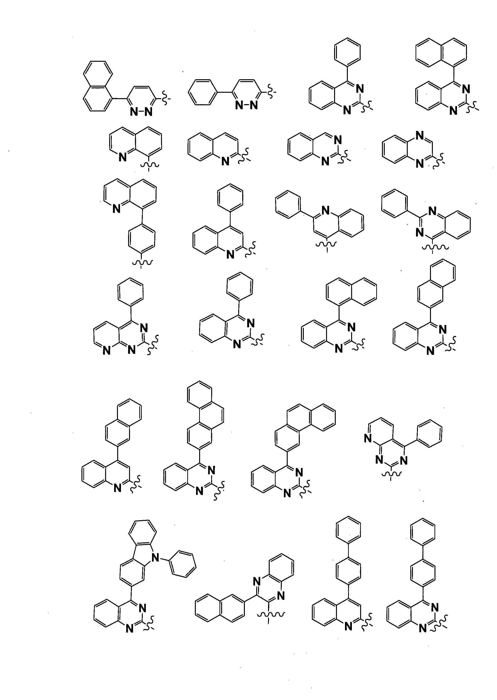
- Het in the formula (1) may be any one selected from the following compounds:
- Z 1, Z 2 , Z 3 and Z 4 are each independently N or CH, provided that at least one of them in each formula is N,
- R 3 is each independently hydrogen, substituted or unsubstituted d- 60 alkyl, substituted Or unsubstituted C 6 -C 60 aryl, or substituted or unsubstituted C 5 -C 60 heteroaryl containing at least one of N, O and S,
- Het in the formula (1) may be any one selected from the group consisting of:
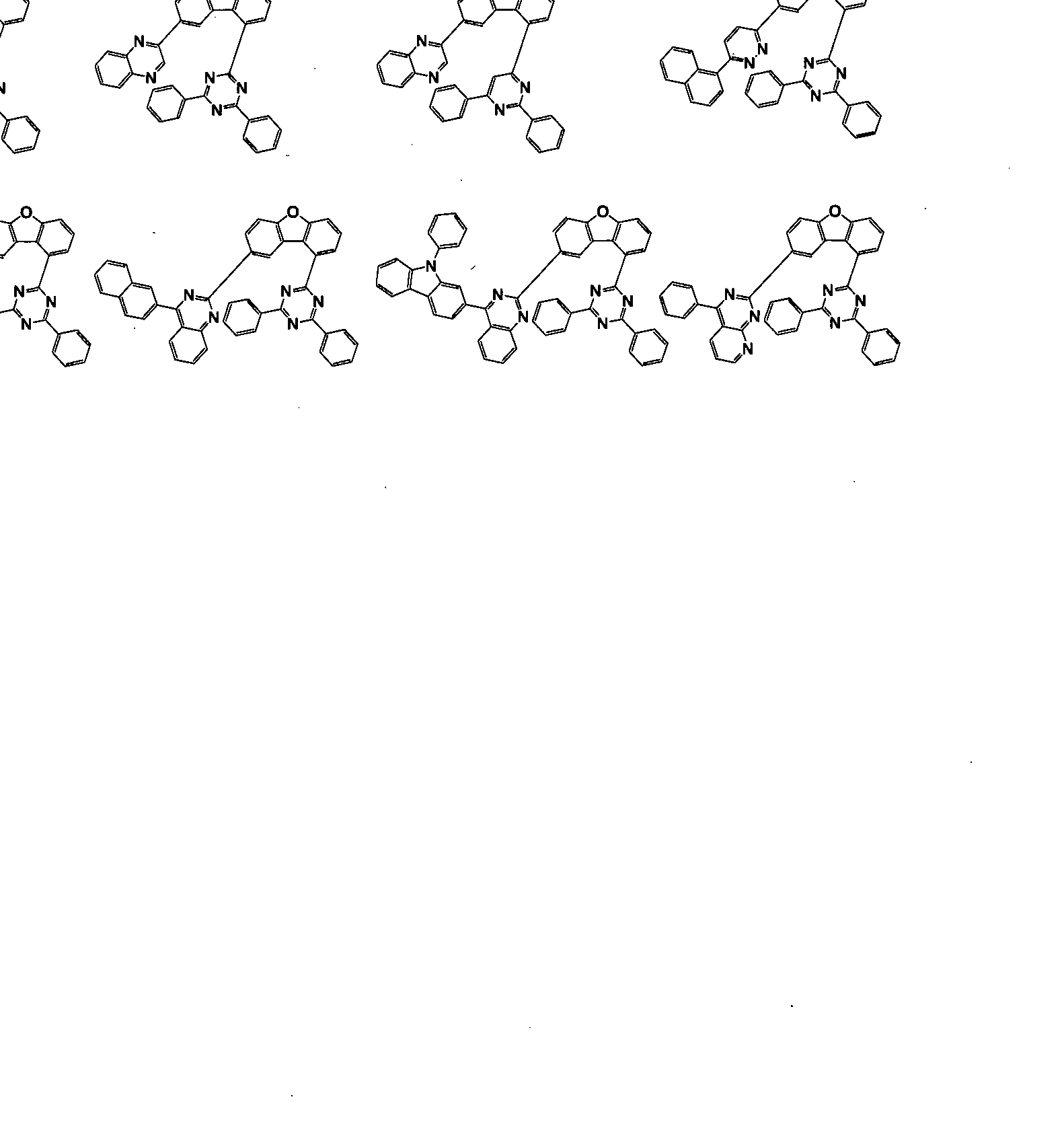
- the compound represented by Formula 1 may be any one selected from the group consisting of:
- the compound represented by the above formula (1) has a structure having a substituent such as triazine (pyridine, pyrimidine) substituted at the 1-position of dibenzofuran (dibenzothiophene) core and the above-described Het substituent simultaneously, Crystallization can be suppressed in addition to excellent heat resistance when the device is driven. Therefore, the organic light emitting device using the organic light emitting device can have a high efficiency, a low driving voltage, a high brightness and a long life.
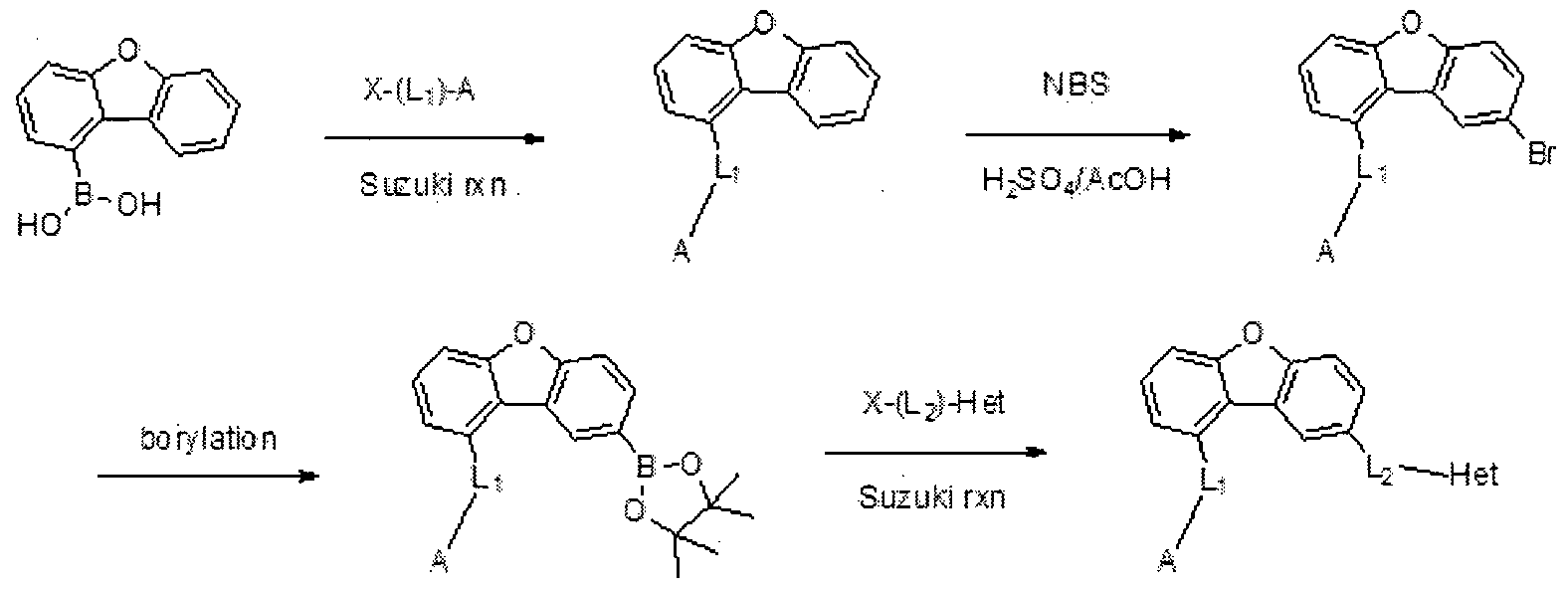
- the compound represented by the formula (1) can be prepared by the same method as in the following reaction formula (1).
- the present invention provides an organic electroluminescent device comprising the compound represented by Formula 1.
- the present invention provides an organic electroluminescent device comprising a first electrode, a second electrode facing the first electrode, And one or more organic layers disposed between the second electrodes, wherein at least one of the organic layers includes a compound represented by Formula 1.
- the organic light emitting device of the present invention may include a hole injection layer, a hole injection layer, a light emitting layer, A hole transport layer, a light emitting layer, an electron transport layer, an electron injection layer, etc.
- the structure of the organic light emitting device is not limited thereto and may include fewer organic layers.
- Layer, a hole transporting layer, or a layer simultaneously injecting and transporting a hole and the hole injecting layer, the hole transporting layer, or the layer simultaneously injecting and transporting a hole transporting compound includes a compound represented by the above formula (1).
- the organic layer may include a light emitting layer, and the light emitting layer includes a compound represented by the general formula (1).
- the organic material layer may include an electron transporting layer or an electron injecting layer, and the electron transporting layer or the electron injecting layer includes the compound represented by the above formula (1).
- the electron transporting layer, the electron injecting layer, or the layer which simultaneously injects electrons and transports electrons includes the compound represented by the above formula (1).
- the compound represented by Formula 1 according to the present invention has excellent thermal stability and has a deep HOMO level of 6.0 eV or more, a high triple energy (ET), and a hole stability.
- the compound represented by the formula (1) is used for an organic material layer capable of electron injection and electron transport at the same time, the n-type dopant used in the art can be commonly used.
- the organic material layer may include a light emitting layer and an electron transporting layer
- the electron transporting layer may include a compound represented by the general formula (1).
- the organic light emitting device according to the present invention may be a normal type organic light emitting device in which an anode, one or more organic layers, and a cathode are sequentially stacked on a substrate.
- the organic light emitting device according to the present invention may be an inverted type organic light emitting device in which a cathode, at least one organic material layer, and an anode are sequentially stacked on a substrate.
- FIGS. Fig. 1 shows an example of an organic light-emitting device comprising a substrate 1, an anode 2, a light-emitting layer 3 and a cathode 4.
- the compound represented by Formula 1 may be included in the light emitting layer.
- 2 is a cross-sectional view of a substrate 1, an anode 2, a hole injecting layer 5, a hole transporting layer 6, a light emitting layer 7, An electron transport layer 8, and a cathode 4.
- the organic light- In such a structure the compound represented by Formula 1 may be included in at least one of the hole injection layer, the hole transport layer, the luminescent compound, and the electron transport layer.
- the organic light emitting device according to the present invention can be manufactured by materials and methods known in the art, except that at least one of the organic material layers includes the compound represented by the above formula (1).
- the organic light emitting diode when the organic light emitting diode includes a plurality of organic layers, the organic layers may be formed of the same material or different materials.
- the organic light emitting device according to the present invention can be manufactured by sequentially laminating a gate electrode, an organic material layer, and a second electrode on a substrate.
- a metal or a metal oxide having conductivity or an alloy thereof is deposited on the substrate by a PVDC photovoltaic deposition method such as a sputtering method or an e-beam evaporation method
- a PVDC photovoltaic deposition method such as a sputtering method or an e-beam evaporation method
- Forming an anode forming an organic material layer including a hole injecting layer, a hole transporting layer, a light emitting layer and an electron transporting layer on the anode, and depositing a material usable as a cathode thereon.
- an organic light emitting device can be formed by sequentially depositing a cathode material, an organic material layer, and a cathode material on a substrate.
- the compound represented by Formula 1 may be formed into an organic layer by a solution coating method as well as a vacuum deposition method in the production of an organic light emitting device.
- the solution coating method refers to spin coating, dip coating, doctor blading, inkjet printing, screen printing, spraying, coating, and the like, but is not limited thereto.
- an organic light emitting device can be manufactured by sequentially depositing an organic material layer and a cathode material from a cathode material on a substrate (WO 2003/012890). However, the manufacturing method is not limited thereto.
- the first electrode may be an anode
- the second electrode may be a cathode
- the first electrode is a cathode
- the second electrode is a cathode.
- the anode material a material having a large work function is preferably used so that hole injection can be smoothly conducted to the organic material layer.
- the positive electrode material include metals such as vanadium, chromium, copper, zinc, and gold, or alloys thereof; Metal oxides such as zinc oxide, indium oxide, indium tin oxide (ITO), and indium zinc oxide (IZO); ⁇ 0: ⁇ 1 SN0 or 2: a combination of a metal and an oxide such as Sb; Poly (3-methylthiophene), poly [3, 4 _ (ethylene -; L, 2--dioxy) thiophene] (PED0T), but a conductive polymer such as a poly blood and, polyaniline, these only limited It is not.
- the negative electrode material is preferably a material having a small work function to facilitate electron injection into the organic material layer.
- the negative electrode material include metals such as magnesium, calcium, sodium, potassium, titanium, indium, yttrium, lithium, gadolinium, aluminum, silver, tin and lead or alloys thereof; Layer structure materials such as LiF / Al or LiO 2 / Al, but the present invention is not limited thereto.
- the hole injecting layer is a layer for injecting holes from an electrode.
- the hole injecting material has a hole injecting effect, and has a hole injecting effect on the light emitting layer or a light emitting material.
- a compound which prevents the migration of excitons to the electron injecting layer or the electron injecting material and is also excellent in the thin film forming ability is preferable.
- the highest occupied molecular orbital (H0M0) of the hole injecting material is preferably between the work function of the anode material and H0M0 of the surrounding organic layer.
- the hole injecting material include organic materials such as porphyrin, oligothiophene, arylamine-based organic materials, quinacridone-based tetraphenylene-based organic materials, quinacridone-based organic materials, perylene ) Organic materials such as anthraquinone, polyaniline, and a polythiophene-based conductive polymer, but the present invention is not limited thereto.
- the hole transport layer receives holes from the hole injection layer
- a material having high mobility to holes is suitable as a material capable of transporting holes from an anode or a hole injection layer to a light emitting layer by using a hole transporting material.
- Specific examples include arylamine-based organic materials, conductive polymers, and block copolymers having a conjugated portion and a non-conjugated portion together, but the present invention is not limited thereto.
- the light emitting material is preferably a material capable of emitting light in the visible light region by transporting and receiving holes and electrons from the hole transporting layer and the electron transporting layer, respectively, and having good quantum efficiency for fluorescence or phosphorescence.
- the light emitting layer may include a host material and a dopant material.
- the host material is a condensed aromatic ring derivative or a heterocyclic compound.
- condensed aromatic ring derivatives include anthracene derivatives, pyrene derivatives, naphthalene derivatives, pentacene derivatives, phenanthrene compounds, and fluoranthene compounds.
- heterocycle-containing compounds include carbazole derivatives, dibenzofuran derivatives, Furan compounds, pyrimidine derivatives, and the like, but are not limited thereto.
- dopant material include aromatic amine derivatives, styrylamine compounds, boron complexes, fluoranthene compounds, and metal complexes.
- aromatic amine derivatives include condensed aromatic ring derivatives having substituted or unsubstituted arylamino groups, and examples thereof include pyrene, anthracene, chrysene, and peripherrhene having an arylamino group.
- styrylamine compound include substituted or unsubstituted Wherein at least one aryl vinyl group is substituted with at least one aryl vinyl group, and at least one substituent selected from the group consisting of an aryl group, a silyl group, an alkyl group, a cycloalkyl group and an arylamino group is substituted or unsubstituted.
- the electron transporting layer is a layer that receives electrons from the electron injecting layer and transports electrons to the light emitting layer.
- the electron transporting material is a material capable of transferring electrons from the cathode well to the light emitting layer. Do. Specific examples include the A1 complex of 8-hydroxyquinoline; Complexes containing Alq 3 ; Organic radical compounds; Hydroxyflavone-metal complexes, and the like, but are not limited thereto.
- the electron transporting layer can be used with any desired cathode material as used according to the prior art.
- a suitable cathode material is a conventional material having a low work function followed by an aluminum layer or a silver layer. Specifically cesium, barium, calcium, ytterbium and samarium, in each case followed by an aluminum layer or a silver layer.
- the electron injection layer is a layer for injecting electrons from the electrode.
- the electron injection layer has an ability to transport electrons, has an electron injection effect from the cathode, and has an excellent electron injection effect with respect to the light emitting layer or the light emitting material. A compound which prevents migration to a layer and is excellent in a thin film forming ability is preferable.
- fluorenone anthraquinodimethane, diphenoquinone, thiopyran dioxide, oxazole, oxadiazole, triazole, imidazole, perylenetetracarboxylic acid, preorenylidene methane, A nitrogen-containing 5-membered ring derivative, and the like, but are not limited thereto.
- Examples of the metal complex compound include 8-hydroxyquinolinato lithium, bis (8-hydroxyquinolinato) zinc, bis (8-hydroxyquinolinato) copper, bis (8- Tris (8-hydroxyquinolinato) aluminum, tris (2-methyl-8-hydroxyquinolinato) aluminum, tris (8- hydroxyquinolinato) gallium, bis (10- Quinolinato) beryllium, bis (10-hydroxybenzo [h] quinolinato) zinc, bis (2-methyl-8- quinolinato) chlorogallium, bis (2-methyl-8-quinolinato) (1-naphthalato) aluminum, bis (2- Quinolinato) (2-naphthalato) gallium, but are not limited thereto.
- the organic light emitting device may be a front emission type, a back emission type, or a both-sided emission type, depending on the material used.
- the compound represented by Formula 1 may be included in an organic solar cell or an organic transistor in addition to an organic light emitting device.
- the preparation of the compound represented by Formula 1 and the organic light emitting device comprising the same will be described in detail in the following examples. However , the following examples are for illustrative purposes only and are not intended to limit the scope of the present invention.
- Example 1 Preparation of Compound 1 9-phenyl-9H-carbazole (7.8 g, 19 mmol) was dissolved in 130 ml of dioxane, and a solution of the compound of formula A-6 (10.0 g, 19 ⁇ ol) (0.09 g, 0.2 mmol) of bis (tri-tert-butylphosphine) paladium (O) was added thereto, followed by heating with stirring for 15 hours. The temperature was lowered to room temperature and filtered. The filtrate was extracted with chloroform and water, and then the organic layer was dried with magnesium sulfate.
- a thin glass substrate coated with ITO (indium tin oxide) at a thickness of 1,300 A was immersed in distilled water containing detergent and washed with ultrasonic waves.
- Fischer Co. product was used as a detergent
- distilled water filtered by a filter of Mi 11 ipore Co. was used as distilled water.
- the ITO was washed for 30 minutes and then washed twice with distilled water and ultrasonically cleaned for 10 minutes. After the distilled water was washed, it was ultrasonically washed with a solvent of isopropyl alcohol, acetone, and methanol, dried, and then transported to a plasma cleaner. Further, the substrate was cleaned using oxygen plasma for 5 minutes, and then the substrate was transported by a vacuum evaporator.
- hexanitrile hexaazatri phenyl ene (HAT) compound was thermally vacuum deposited to a thickness of 50 A on the ⁇ key transparent electrode prepared as described above to form a hole injection layer.
- N-phenylamino] biphenyl (NPB; HT-1) which is a material for transporting holes
- a hole transport layer was formed by thermal vacuum deposition to form a HT-2 compound on the HT-1 vapor deposition layer, and an electron blocking layer was formed by vacuum evaporation of the HT-2 compound to a thickness of 50A.
- Compound 2 the following YGH-1 compound, and phosphorescence YGD-1, which were prepared as a host, were co-deposited on the HT-2 deposited film at a weight ratio of 44: 44: 12 to form a 400 A thick light emitting layer.
- An ET-1 material was vacuum-deposited on the light-emitting layer to a thickness of 250 A, and an ET-2 material was co-deposited with a 2% weight ratio Li to a thickness of 100 A to form an electron transport layer and an electron injection layer.
- Aluminum was deposited on the electron injection layer to a thickness of 1000 A to form a cathode.
- the deposition rate of the organic material was maintained at 0.4 - 0.7 A / sec
- the deposition rate of aluminum was maintained at 2 A / sec
- the vacuum degree during the deposition was maintained at 1 ⁇ 10 7 to 5 ⁇ 10 - 8 torr
- T95 means the time required for the luminance to be reduced to 95% from the initial luminance.
- substrate 2 anode
Landscapes
- Chemical & Material Sciences (AREA)
- Organic Chemistry (AREA)
- Physics & Mathematics (AREA)
- Optics & Photonics (AREA)
- Spectroscopy & Molecular Physics (AREA)
- Engineering & Computer Science (AREA)
- Materials Engineering (AREA)
- Electroluminescent Light Sources (AREA)
Abstract
본 발명은 신규한 헤테로 고리 화합물 및 이를 이용한 유기 발광 소자를 제공한다.
Description
【발명의 명칭】
신규한 헤테로 고리 화합물 및 이를 이용한 유기 발광 소자 【기술분야】
관련 출원 (들)과의 상호 인용
본 출원은 2017년 7월 20일자 한국 특허 출원 제 10-2017-0092174호 및 2018년 7월 19일자 한국 특허 출원 제 10-2018-0084350호에 기초한 우선권의 이익을 주장하며, 해당 한국 특허 출원들의 문헌에 개시된 모든 내용은 본 명세서의 일부로서 포함된다.
본 발명은 신규한 헤테로 고리 화합물 및 이를 포함하는 유기 발광 소자에 관한 것이다.
【발명의 배경이 되는 기술】
일반적으로 유기 발광 현상이란 유기 물질을 이용하여 전기에너지를 빛에너지로 전환시켜주는 현상을 말한다. 유기 발광 현상을 이용하는 유기 발광 소자는 넓은 시야각, 우수한 콘트라스트, 빠른 웅답 시간을 가지며, 휘도, 구동 전압 및 응답 속도 특성이 우수하여 많은 연구가 진행되고 있다. 유기 발광 소자는 일반적으로 양극과 음극 및 상기 양극과 음극 사이에 유기물 층을 포함하는 구조를 가진다. 상기 유기물 층은 유기 발광 소자의 효율과 안정성을 높이기 위하여 각기 다른 물질로 구성된 다층의 구조로 이루어진 경우가 많으며, 예컨대 정공주입층, 정공수송층, 발광층, 전자수송층, 전자주입층 등으로 이루어질 수 있다. 이러한 유기 발광 소자의 구조에서 두 전극 사이에 전압을 걸어주게 되면 양극에서는 정공이, 음극에서는 전자가 유기물층에 주입되게 되고, 주입된 정공과 전자가 만났을 때 엑시톤 (exci ton)이 형성되며, 이 액시톤이 다시 바닥상태로 떨어질 때 빛이 나게 된다. 상기와 같은 유기 발광 소자에 사용되는 유기물에 대하여 새로운 재료의 개발이 지속적으로 요구되고 있다.
【선행기술문헌】
【특허문헌】
(특허문헌 0001) 한국특허 공개번호 제 10-2013-073537호
【발명의 내용】
【해결하고자 하는 과제】
본 발명은 신규한 헤테로고리 화합물 화합물 및 이를 포함하는 유기 발광 소자에 관한 것이다.
【과제의 해결 수단】
본 발명은 하기 화학식 1로 표시되는 화합물을 제공한다.

상기 화학식 1에서,
¾은 0또는 S이고,
^는 수소 또는 치환 또는; 비치환된 d-so의 알킬이고,
Li 및 L2는 각각 독립적으로 직접 결합 또는 치환 또는 비치환된 C6-60 아릴렌이고,
Yi , Y2 및 Υ3는 각각 독립적으로 Ν 또는 CR2이고, 단 이들 중 하나 이상이 N이고, ¾는 수소 또는 치환 또는 비치환된 의 알킬이고,
An 및 Ar2는 각각 독립적으로 치환 또는 비치환된 C6-60 아릴 또는 N, 0 및 S 중 1개 이상을 포함하는 치환 또는 비치환된 C5-60 헤테로아릴이고, 이들은 인접한 Yi , Y2 및 Υ3와 결합하여 고리를 형성할 수 있고,
Het는 하나 이상의 N을 포함하는 치환 또는 비치환된 C5-60 헤테로아릴이고,
m 및 n은 각각 독립적으로 1 또는 2임 또한, 본 발명은 제 1 전극; 상기 제 1 전극과 대향하여 구비된 제 2 전극; 및 상기 제 1 전극과 상기 계 2 전극 사이에 구비된 1층 이상의 유기물층을 포함하는 유기 발광 소자로서, 상기 유기물층 중 1층 이상은 전술한 본 발명의 화합물을 포함하는 유기 발광 소자를 제공한다.
【발명의 효과】
상술한 화학식 1로 표시되는 화합물은 유기 발광 소자의 유기물 층의 재료로서 사용될 수 있으며, 유기 발광 소자에서 효율의 향상, 낮은 구동전압 및 /또는 수명 특성을 향상시킬 수 있다. 특히, 상술한 화학식 1로 표시되는 화합물은 정공주입, 정공수송, 정공주입 및 수송, 발광, 전자수송, 또는 전자주입 재료로 사용될 수 있다. 【도면의 간단한 설명】
도 1은 기판 ( 1), 양극 (2), 발광층 (3), 음극 (4)으로 이루어진 유기 발광 소자의 예를 도시한 것이다.
도 2는 기판 ( 1), 양극 (2) , 정공주입층 (5), 정공수송층 (6), 발광층 (7), 전자수송층 (8) 및 음극 (4)으로 이루어진 유기 발광 소자의 예를 도시한 것이다.
【발명을 실시하기 위한 구체적인 내용】
이하, 본 발명의 이해 ¾ 돕기 위하여 보다 상세히 설명한다. 본 발명은 하기 화학식 1로 표시되는 화합물을 제공한다.
하기 화학식 1로 표시되는 화합물 :
[화학식 1]

상기 화학식 1에서,
¾은 0 또는 S이고,
¾는 수소 또는 치환 또는 비치환된 d-60의 알킬이고,
및 1^2는 각각 독립적으로 직접 결합 또는 치환 또는 비치환된 C6-60 아릴렌이고,
Yi , Y2 및 Υ3는 각각 독립적으로 Ν 또는 CR2이고, 단 이들 중 하나 이상이 N이고, R2는 수소 또는 치환 또는 비치환된 d— 60의 알킬이고,
An 및 Ar2는 각각 독립적으로 치환 또는 비치환된 C6-60 아릴 또는 N , 0 및 S 중 1개 이상을 포함하는 치환 또는 비치환된 C5-60 헤테로아릴이고, 이들은 인접한 ^, Y2 및 Υ3와 결합하여 고리를 형성할 수 있고,
Het는 하나 이상의 N을 포함하는 치환 또는 비치환된 C5-60 헤테로아릴이고,
m 및 n은 각각 독립적으로 1 또는 2이다.
본 명세서에서, ᅥᅳ는 다른 치환기에 연결되는 결합을 의미한다. 본 명세서에서 "치환 또는 비치환된" 이라는 용어는 중수소; 할로겐기; 니트릴기; 니트로기; 히드록시기; 카보닐기; 에스테르기; 이미드기; 아미노기; 포스핀옥사이드기; 알콕시기; 아릴옥시기; 알킬티옥시기; 아릴티옥시기; 알킬술폭시기; 아릴술폭시기; 실릴기; 붕소기; 알킬기; 사이클로알킬기; 알케닐기; 아릴기; 아르알킬기; 아르알케닐기; 알킬아릴기; 알킬아민기; 아랄킬아민기; 헤테로아릴아민기; 아릴아민기; 아릴포스핀기; 또는 N, 0 및 S 원자 중 1개 이상을 포함하는 헤테로고리기로 이루어진 군에서 선택된 1개 이상의 치환기로 치환 또는 비치환되거나, 상기 예시된 치환기 중 2 이상의
치환기가 연결된 치환 또는 비치환된 것을 의미한다. 예컨대, "2 이상의 치환기가 연결된 치환기 "는 비페닐기일 수 있다. 즉, 비페닐기는 아릴기일 수도 있고, 2개의 페닐기가 연결된 치환기로 해석될 수 있다. 본 명세서에서 카보닐기의 탄소수는 특별히 한정되지 않으나, 탄소수 1 내지 40인 것이 바람직하다. 구체적으로 하기와 같은 구조의 화합물이 될 수 있으나, 이에 한정되는 것은 아니다.


경
 등。 될 수 있다. 다만, 이에 한정되 것은 아니다. 본 명세서에 있어서, 헤테로고리기는 이종 원소로 0, N, Si 및 S 중 1개 이상을 포함하는 헤테로고리기로서, 탄소수는 특별히 한정되지 않으나, 탄소수 2 내지 60인 것이 바람직하다. 헤테로고리기의 예로는 티오펜기, 퓨란기, 피를기, 이미다졸기, 티아졸기, 옥사졸기, 옥사디아졸기, 트리아졸기, 피리딜기, 비피리딜기, 피리미딜기, 트리아진기, 트리아졸기, 아크리딜기, 피리다진기, 피라지닐기, 퀴놀리닐기, 퀴나졸린기, 퀴녹살리닐기, 프탈라지닐기, 피리도 피리미디닐기, 피리도 피라지닐기, 피라지노 피라지닐기, 이소퀴놀린기, 인돌기, 카바졸기, 벤조옥사졸기, 벤조이미다졸기, 벤조티아졸기, 벤조카바졸기, 벤조티오펜기, 디벤조티오펜기, 벤조퓨라닐기, 페난쓰를린기 (phenanthrol ine) , 티아졸릴기, 이소옥사졸릴기, 옥사디아졸릴기, 티아디아졸릴기, 벤조티아졸릴기, 페노티아지닐기 및 디벤조퓨라닐기 등이 있으나, 이들에만 한정되는 것은 아니다. 본 명세서에 있어서, 아르알킬기, 아르알케닐기, 알킬아릴기, 아릴아민기 중의 아릴기는 전술한 아릴기의 예시와 같다. 본 명세서에 있어서, 아르알킬기, 알킬아릴기, 알킬아민기 중 알킬기는 전술한 알킬기의 예시와 같다. 본 명세서에 있어서, 헤테로아릴아민 중 헤테로아릴은 전술한 헤테로고리기에 관한 설명이 적용될 수 있다. 본 명세서에 있어서, 아르알케닐기 중 알케닐기는 전술한 알케닐기의 예시와 같다. 본 명세서에 있어서, 아릴렌은 2가기인 것을 제외하고는 전술한 아릴기에 관한 설명이 적용될 수 있다. 본 명세서에 있어서, 헤테로아릴렌은 2가기인 것을 제외하고는 전술한 헤테로고리기에 관한 설명이 적용될 수 있다. 본 명세서에
있어서, 탄화수소 고리는 1가기가 아니고, 2개의 치환기가 결합하여 형성한 것을 제외하고는 전술한 아릴기 또는 사이클로알킬기에 관한 설명아 적용될 수 있다. 본 명세서에 있어서, 헤테로고리는 1가기가 아니고, 2개의 치환기가 결합하여 형성한 것을 제외하고는 전술한 헤테로고리기에 관한 설명이 적용될 수 있다. 바람직하게는, 상기 화학식 1로 표시되는 화합물은 하기 화학식 2 내지 6으로 표시되는 화합물 중에서 선택되는 어느 하나일 수 있다.
등。 될 수 있다. 다만, 이에 한정되 것은 아니다. 본 명세서에 있어서, 헤테로고리기는 이종 원소로 0, N, Si 및 S 중 1개 이상을 포함하는 헤테로고리기로서, 탄소수는 특별히 한정되지 않으나, 탄소수 2 내지 60인 것이 바람직하다. 헤테로고리기의 예로는 티오펜기, 퓨란기, 피를기, 이미다졸기, 티아졸기, 옥사졸기, 옥사디아졸기, 트리아졸기, 피리딜기, 비피리딜기, 피리미딜기, 트리아진기, 트리아졸기, 아크리딜기, 피리다진기, 피라지닐기, 퀴놀리닐기, 퀴나졸린기, 퀴녹살리닐기, 프탈라지닐기, 피리도 피리미디닐기, 피리도 피라지닐기, 피라지노 피라지닐기, 이소퀴놀린기, 인돌기, 카바졸기, 벤조옥사졸기, 벤조이미다졸기, 벤조티아졸기, 벤조카바졸기, 벤조티오펜기, 디벤조티오펜기, 벤조퓨라닐기, 페난쓰를린기 (phenanthrol ine) , 티아졸릴기, 이소옥사졸릴기, 옥사디아졸릴기, 티아디아졸릴기, 벤조티아졸릴기, 페노티아지닐기 및 디벤조퓨라닐기 등이 있으나, 이들에만 한정되는 것은 아니다. 본 명세서에 있어서, 아르알킬기, 아르알케닐기, 알킬아릴기, 아릴아민기 중의 아릴기는 전술한 아릴기의 예시와 같다. 본 명세서에 있어서, 아르알킬기, 알킬아릴기, 알킬아민기 중 알킬기는 전술한 알킬기의 예시와 같다. 본 명세서에 있어서, 헤테로아릴아민 중 헤테로아릴은 전술한 헤테로고리기에 관한 설명이 적용될 수 있다. 본 명세서에 있어서, 아르알케닐기 중 알케닐기는 전술한 알케닐기의 예시와 같다. 본 명세서에 있어서, 아릴렌은 2가기인 것을 제외하고는 전술한 아릴기에 관한 설명이 적용될 수 있다. 본 명세서에 있어서, 헤테로아릴렌은 2가기인 것을 제외하고는 전술한 헤테로고리기에 관한 설명이 적용될 수 있다. 본 명세서에
있어서, 탄화수소 고리는 1가기가 아니고, 2개의 치환기가 결합하여 형성한 것을 제외하고는 전술한 아릴기 또는 사이클로알킬기에 관한 설명아 적용될 수 있다. 본 명세서에 있어서, 헤테로고리는 1가기가 아니고, 2개의 치환기가 결합하여 형성한 것을 제외하고는 전술한 헤테로고리기에 관한 설명이 적용될 수 있다. 바람직하게는, 상기 화학식 1로 표시되는 화합물은 하기 화학식 2 내지 6으로 표시되는 화합물 중에서 선택되는 어느 하나일 수 있다.

[화학식 5]

Y3^Y2
An
상기 화학식 2 내지 6에서,
Xi, , , Het, Yi, Y2) Υ3, Ri, Arlf Ar2 및 n은 청구항 1에서 정의한 바와 같다. 더욱 바람직하게는, 상기 화학식 1로 표시되는 화합물은 상기 화학식 2, 4, 6으로 표시되는 화합물일 수 있다. 또한, 바람직하게는, 상기 화학식 1의 화합물은 하기 화학식 7 내지 11로 표시되는 화합물 중에서 선택되는 어느 하나일 수 있다.

[화학식 8]

상기 화학식 5 내지 11에서,
Xi, Li, L2, Het, Ri, n 및 m은 앞서 정의한 바와 같다.
바람직하게는, 상기 화학식 1에서 Rr 수소 또는 치환 또는 비치환된 Cwo의 알킬일 수 있으며, 더욱 바람직하게는 수소일 수 있다. 바람직하게는, 상기 화학식 1에서 및 L2는 각각 독립적으로 직접 결합 또 일 수 있다. 바람직하게는, 상기 화학식 1에서 Het 는 하기로 표시되는 화합물 중에서 선택되는 어느 하나일 수 있다:

[1-1】 [1-2] [1-3] [1-4] [1-5] [1-6】

B는 0또는 S이고,
Z1 ( Z2, Z3 및 Z4는 각각 독립적으로 N 또는 CH이며, 단, 각 화학식 내에서 이들 중 하나 이상이 N이고,
R3는 각각 독립적으로 수소, 치환 또는 비치환된 d— 60의 알킬, 치환
또는 비치환된 C6-60 아릴, 또는 N , 0 및 S 중 1개 이상을 포함하는 치환 또는 비치환된 C5-60 헤테로아릴이고,
1 은 각각 독립적으로 1 또는 2이다. 바람직하게는, 상기 ¾은 수소 또는 하기로 이루어진 군에서 선택되는 어느 하


Ζ£Ζ800/8Ϊ0ΖΗΜ/Χ3<Ι 0£Ζ.Ζ.ΐΟ/6ΐΟΖ OAV

9L

Z£Z800/8lOZW^/13d ocz.z.io/6ioz OA
Li

ZCZ800/8lOZaM/X3d ocz.z.io/6ioz OAV

Z£Z800/8lOZW^/13d ocz.z.io/6ioz OA
6L

Z£Z800/8lOZW^/13d ocz.z.io/6ioz OA
oz

ZCZ800/8lOZaM/X3d ocz.z.io/6ioz OAV

ZCZ800/8lOZaM/X3d ocz.z.io/6ioz OAV

ZCZ800/8lOZaM/X3d ocz.z.io/6ioz OAV

상기 화학식 1로 표시되는 화합물은, 디벤조푸란 (디벤조싸이오펜) 코어의 1번 위치에 치환된 트리아진 (피리딘, 피리미딘) 등의 치환기와 상술한 Het 치환기를 동시에 갖는 구조를 가짐으로써, 소자 내 구동시 내열성이 우수함과 더불어, 결정화를 억제시킬 수 있다. 따라서, 이를 이용한 유기 발광 소자는 고효율, 저 구동 전압, 고휘도 및 장수명 등을 가질 수 있다. 상기 화학식 1로 표시되는 화합물은 하기 반웅식 1과 같은 제조 방법으로 제조할 수 있다.
[반웅식 1]
A= ΥγΑ
¾†^¾
Ar,
상기 반웅식 1에서, , L2, Yi , Y2 , Y3 , Ar1 ( Ar2 및 Het는 앞서 정의한 바와 같다. 상기 반응식에 사용된 반웅기 및 촉매의 종류는 적절하게 변경 가능하다. 또한, 본 발명은 상기 화학식 1로 표시되는 화합물을 포함하는 유기 발광 소자를 제공한다. 일례로, 본 발명은 제 1 전극; 상기 제 1 전극과 대향하여 구비된 제 2 전극; 및 상기 게 1 전극과 상기 제 2 전극 사이에 구비된 1층 이상의 유기물 층을 포함하는 유기 발광 소자로서, 상기 유기물층 중 1층 이상은 상기 화학식 1로 표시되는 화합물을 포함하는, 유기 발광 소자를 제공한다. 본 발명의 유기 발광 소자의 유기물 층은 단층 구조로 이루어질 수도 있으나, 2층 이상의 유기물층이 적층된 다층 구조로 이루어질 수 있다. 예컨대, 본 발명의 유기 발광 소자는 유기물 충으로서 정공주입층, 정공수송층, 발광층, 전자수송층, 전자주입층 등을 포함하는 구조를 가질 수 있다. 그러나 유기 발광 소자의 구조는 이에 한정되지 않고 더 적은 수의 유기층을 포함할 수 있다. 또한, 상기 유기물 층은 장공주입층, 정공수송층, 또는 정공 주입과 수송을 동시에 하는 층을 포함할 수 있고, 상기 정공주입층, 정공수송층, 또는 정공 주입과 수송을 동시에 하는 층은 상기 화학식 1로 표시되는 화합물을 포함한다.
또한, 상기 유기물 층은 발광층을 포함할 수 있고, 상기 발광층은 상기 화학식 1로 표시되는 화합물을포함한다. 또한, 상기 유기물 층은 전자수송층, 또는 전자주입층을 포함할 수 있고, 상기 전자수송층, 또는 전자주입층은 상기 화학식 1로 표시되는 화합물을 포함한다. 또한, 상기 전자수송층, 전자주입층, 또는 전자 주입 및 전자 수송을 동시에 하는 층은 상기 화학식 1로 표시되는 화합물을 포함한다. 특히, 본 발명에 따른 화학식 1로 표시되는 화합물은 열적 안정성이 우수하고, 6.0 eV 이상의 깊은 HOMO 준위, 높은 삼중함 에너지 (ET) , 및 정공 안정성을 가지고 있다. 또한, 상기 화학식 1로 표시되는 화합물을 전자 주입 및 전자 수송을 동시에 할 수 있는 유기물 층에 사용할 경우, 당업계에서 사용하는 n-형 도펀트를 흔합하여 사용할 수 있다. 또한, 상기 유기물 층은 발광층 및 전자수송층을 포함하고, 상기 전자수송층은 상기 화학식 1로 표시되는 화합물을포함할수 있다. 또한, 본 발명에 따른 유기 발광 소자는, 기판상에 양극, 1층 이상의 유기물 층 및 음극이 순차적으로 적층된 구조 (normal type)의 유기 발광 소자일 수 있다. 또한, 본 발명에 따른 유기 발광 소자는 기판상에 음극, 1층 이상의 유기물 층 및 양극이 순차적으로 적층된 역방향 구조 ( inverted type)의 유기 발광 소자일 수 있다. 예컨대 본 발명의 일실시예에 따른 유기 발광 소자의 구조는 도 1 및 2에 예시되어 있다. 도 1은 기판 ( 1) , 양극 (2), 발광층 (3), 음극 (4)으로 이루어진 유기 발광 소자의 예를 도시한 것이다. 이와 같은 구조에 있어서, 상기 화학식 1로 표시되는 화합물은상기 발광층에 포함될 수 있다. 도 2는 기판 ( 1), 양극 (2), 정공주입층 (5), 정공수송층 (6), 발광층 (7),
전자수송층 (8) 및 음극 (4)로 이루어진 유기 발광 소자의 예를 도시한 것이다. 이와 같은 구조에 있어서, 상기 화학식 1로 표시되는 화합물은 상기 정공주입층, 정공수송층, 발광충 및 전자수송층 중 1층 이상에 포함될 수 있다. 본 발명에 따른 유기 발광 소자는, 상기 유기물 층 중 1층 이상이 상기 화학식 1로 표시되는 화합물을 포함하는 것을 제외하고는 당 기술분야에 알려져 있는 재료와 방법으로 제조될 수 있다. 또한, 상기 유기 발광 소자가 복수개의 유기물층을 포함하는 경우, 상기 유기물층은 동일한 물질 또는 다른 물질로 형성될 수 있다. 예컨대, 본 발명에 따른 유기 발광 소자는 기판 상에 게 1 전극, 유기물층 및 제 2 전극을 순차적으로 적층시켜 제조할 수 있다. 이때, 스퍼터링법 (sputter ing)이나 전자빔 증발법 (e—beam evaporat ion)과 같은 PVDCphysi cal Vapor Depos i t ion)방법을 이용하여, 기판 상에 금속 또는 전도성을 가지는 금속 산화물 또는 이들의 합금을 증착시켜 양극을 형성하고, 그 위에 정공 주입층, 정공 수송층, 발광층 및 전자 수송층을 포함하는 유기물 층을 형성한 후, 그 위에 음극으로 사용할 수 있는 물질을 증착시켜 제조할 수 있다. 이와 같은 방법 외에도, 기판 상에 음극 물질부터 유기물층, 양극 물질을 차례로 증착시켜 유기 발광 소자를 만들 수 있다. 또한, 상기 화학식 1로 표시되는 화합물은 유기 발광 소자의 제조시 진공 증착법 뿐만 아니라 용액 도포법에 의하여 유기물 층으로 형성될 수 있다. 여기서, 용액 도포법이라 함은 스핀 코팅, 딥코팅, 닥터 블레미딩, 잉크젯 프린팅, 스크린 프린팅, 스프레이법, 를 코팅 등을 의미하지만, 이들만으로 한정되는 것은 아니다. 이와 같은 방법 외에도, 기판 상에 음극 물질로부터 유기물층, 양극 물질을 차례로 증착시켜 유기 발광 소자를 제조할 수 있다 (W0 2003/012890) . 다만, 제조 방법이 이에 한정되는 것은 아니다. 일례로, 상기 게 1 전극은 양극이고, 상기 게 2 전극은 음극이거나,
또는 상기 제 1 전극은 음극이고, 상기 제 2 전극은 양극이다. 상기 양극 물질로는 통상 유기물 층으로 정공 주입이 원활할 수 있도록 일함수가 큰 물질이 바람직하다. 상기 양극 물질의 구체적인 예로는 바나듐, 크름, 구리, 아연, 금과 같은 금속 또는 이들의 합금; 아연 산화물, 인듐 산화물, 인듐주석 산화물 ( ITO) , 인듐아연 산화물 ( IZ0)과 같은 금속 산화물; Ζη0:Α1 또는 SN02 : Sb와 같은 금속과 산화물의 조합; 폴리 (3- 메틸티오펜), 폴리 [3,4_ (에틸렌- ;L , 2-디옥시)티오펜] (PED0T) , 폴리피를 및 폴리아닐린과 같은 전도성 고분자 등이 있으나, 이들에만 한정되는 것은 아니다. 상기 음극 물질로는 통상 유기물층으로 전자 주입이 용이하도록 일함수가 작은 물질인 것이 바람직하다. 상기 음극 물질의 구체적인 예로는 마그네슘, 칼슘, 나트륨, 칼륨, 티타늄, 인듐, 이트륨, 리튬, 가돌리늄, 알루미늄, 은, 주석 및 납과 같은 금속 또는 이들의 합금; LiF/Al 또는 Li02/Al과 같은 다층 구조 물질 등이 있으나, 이들에만 한정되는 것은 아니다. 상기 정공주입층은 전극으로부터 정공을 주입하는 층으로, 정공 주입 물질로는 정공을 수송하는 능력을 가져 양극에서의 정공 주입효과, 발광층 또는 발광재료에 대하여 우수한 정공 주입 효과를 갖고, 발광층에서 생성된 여기자의 전자주입층 또는 전자주입재료에의 이동을 방지하며, 또한, 박막 형성 능력이 우수한 화합물이 바람직하다. 정공 주입 물질의 H0M0(highest occupied molecular orbi tal )가 양극 물질의 일함수와 주변 유기물 층의 H0M0 사이인 것이 바람직하다. 정공 주입 물질의 구체적인 예로는 금속 포피린 (porphyr in) , 올리고티오펜, 아릴아민 계열의 유기물, 핵사니트릴핵사아자트리페닐렌 계열의 유기물, 퀴나크리돈 (quinacr idone)계열의 유기물, 페릴렌 (perylene) 계열의 유기물ᅳ 안트라퀴논 및 폴리아닐린과 폴리티오펜 계열의 전도성 고분자 등이 있으나, 이들에만 한정 되는 것은 아니다. 상기 정공수송층은 정공주입층으로부터 정공을 수취하여 발광층까지
정공을 수송하는 층으로, 정공 수송 물질로 양극이나 정공 주입층으로부터 정공을 수송받아 발광층으로 옮겨줄 수 있는 물질로 정공에 대한 이동성이 큰 물질이 적합하다. 구체적인 예로는 아릴아민 계열의 유기물, 전도성 고분자, 및 공액 부분과 비공액 부분이 함께 있는 블록 공중합체 등어 있으나, 이들에만 한정되는 것은 아니다. 상기 발광 물질로는 정공 수송층과 전자 수송층으로부터 정공과 전자를 각각 수송받아 결합시킴으로써 가시광선 영역의 빛을 낼 수 있는 물질로서, 형광이나 인광에 대한 양자 효율이 좋은 물질이 바람직하다. 구체적인 예로 8-히드록시-퀴놀린 알루미늄 착물 (Alq3) ; 카르바졸 계열 화합물; 이량체화 스티릴 (dimer i zed styryl ) 화합물; BAl q ; 10—히드록시벤조 퀴놀린—금속 화합물; 벤족사졸, 벤즈티아졸 및 벤즈이미다졸 계열의 화합물; 폴리 (P-페닐렌비닐렌) (PPV) 계열의 고분자; 스피로 (spi ro) 화합물; 폴리플루오렌, 루브렌 등이 있으나, 이들에만 한정되는 것은 아니다. 상기 발광층은 호스트 재료 및 도펀트 재료를 포함할 수 있다. 호스트 재료는 축합 방향족환 유도체 또는 헤테로환 함유 화합물 등이 있다. 구체적으로 축합 방향족환 유도체로는 안트라센 유도체, 피렌 유도체, 나프탈렌 유도체, 펜타센 유도체, 페난트렌 화합물, 플루오란텐 화합물 등이 있고, 헤테로환 함유 화합물로는 카바졸 유도체, 디벤조퓨란 유도체, 래더형 퓨란 화합물, 피리미딘 유도체 등이 있으나, 이에 한정되지 않는다. 도펀트 재료로는 방향족 아민 유도체, 스트릴아민 화합물, 붕소 착체, 플루오란텐 화합물, 금속 착체 등이 있다. 구체적으로 방향족 아민 유도체로는 치환 또는 비치환된 아릴아미노기를 갖는 축합 방향족환 유도체로서, 아릴아미노기를 갖는 피렌, 안트라센, 크리센, 페리플란텐 등이 있으며, 스티릴아민 화합물로는 치환 또는 비치환된 아릴아민에 적어도 1개의 아릴비닐기가 치환되어 있는 화합물로, 아릴기, 실릴기, 알킬기, 사이클로알킬기 및 아릴아미노기로 이루어진 군에서 1 또는 2 이상 선택되는 치환기가 치환 또는 비치환된다. 구체적으로 스티릴아민, 스티릴디아민, 스티릴트리아민, 스티릴테트라아민 등이 있으나, 이에 한정되지 않는다. 또한,
금속 착체로는 이리듐 착체, 백금 착체 등이 있으나, 이에 한정되지 않는다. 상기 전자수송층은 전자주입층으로부터 전자를 수취하여 발광층까지 전자를 수송하는 층으로 전자 수송 물질로는 음극으로부터 전자를 잘 주입 받아 발광층으로 옮겨줄 수 있는 물질로서, 전자에 대한 이동성이 큰 물질이 적합하다. 구체적인 예로는 8-히드록시퀴놀린의 A1 착물; Alq3를 포함한 착물; 유기 라디칼 화합물; 히드록시플라본 -금속 착물 등이 있으나, 이들에만 한정되는 것은 아니다. 전자 수송층은 종래기술에 따라 사용된 바와 같이 임의의 원하는 캐소드 물질과 함께 사용할 수 있다. 특히, 적절한 캐소드 물질의 예는 낮은 일함수를 가지고 알루미늄층 또는 실버층이 뒤따르는 통상적인 물질이다. 구체적으로 세슘, 바륨, 칼슘, 이테르븀 및 사마륨이고, 각 경우 알루미늄 층 또는 실버층이 뒤따른다. 상기 전자 주입층은 전극으로부터 전자를 주입하는 층으로, 전자를 수송하는 능력을 갖고, 음극으로부터의 전자 주입 효과, 발광층 또는 발광 재료에 대하여 우수한 전자주입 효과를 가지며, 발광층에서 생성된 여기자의 정공주입층에의 이동을 방지하고, 또한, 박막형성능력이 우수한 화합물이 바람직하다. 구체적으로는 플루오레논, 안트라퀴노다이메탄, 다이페노퀴논, 티오피란 다이옥사이드, 옥사졸, 옥사다이아졸, 트리아졸, 이미다졸, 페릴렌테트라카복실산, 프레오레닐리덴 메탄, 안트론 등과 그들의 유도체, 금속 착체 화합물 및 질소 함유 5원환 유도체 등이 있으나, 이에 한정되지 않는다. 상기 금속 착체 화합물로서는 8-하이드록시퀴놀리나토 리튬, 비스 (8- 하이드록시퀴놀리나토)아연, 비스 (8-하이드록시퀴놀리나토)구리, 비스 (8- 하이드록시퀴놀리나토)망간, 트리스 (8-하이드록시퀴놀리나토)알루미늄, 트리스 (2-메틸 -8—하이드록시퀴놀리나토)알루미늄, 트리스 (8- 하이드록시퀴놀리나토)갈륨, 비스 ( 10—하이드록시벤조 [h]퀴놀리나토)베릴륨, 비스 ( 10-하이드록시벤조 [h]퀴놀리나토)아연, 비스 (2-메틸 -8- 퀴놀리나토)클로로갈륨, 비스 (2-메틸 -8-퀴놀리나토) ( 0-크레졸라토)갈륨, 비스 (2-메틸 -8-퀴놀리나토) ( 1-나프를라토)알루미늄, 비스 (2-메틸 -8-
퀴놀리나토) (2-나프를라토)갈륨 등이 있으나, 이에 한정되지 않는다. 본 발명에 따른 유기 발광 소자는 사용되는 재료에 따라 전면 발광형, 후면 발광형 또는 양면 발광형일 수 있다. 또한, 상기 화학식 1로 표시되는 화합물은 유기 발광 소자 외에도 유기 태양 전지 또는 유기 트랜지스터에 포함될 수 있다. 상기 화학식 1로 표시되는 화합물 및 이를 포함하는 유기 발광 소자의 제조는 이하 실시예에서 구체적으로 설명한다. 그러나 '하기 실시예는 본 발명을 예시하기 위한 것이며, 본 발명의 범위가 이들에 의하여 한정되는 것은 아니다. 제조예 1

1) 화합물 A-1의 제조
1-브로모 -3-플루오로 -2-아이오도벤젠 (75 g, 249.3 匪 ol ) , (5-클로로- 2-메록시페닐)보론산 (51. 1 g, 249.3 mmol )을 테트라하이드로퓨란 550 mL에 녹였다. 여기에 탄산나트륨 (Na2C03) 2 M 용액 (350 mL) , 테트라키스 (트리페닐포스핀)팔라듐 (0) (2 · 88 g, 2.49 mmol )을 넣고 11시간 환류시켰다. 반웅이 끝난 후 상온으로 넁각시키고, 물 층을 분리하여 제거하고 무수황산마그네슘으로 건조한 후 감압농축 시킨 흔합물을 클로로포름과
에탄올을 이용하여 재결정화시켜 화합물 A-1 (63.2 g, 수율 80 %; MS:[M+H]+=314)을 얻었다.
2) 화합물 A-2의 제조
화합물 A-1 (63.2 g, 200.3 隱 οθ올 디클로로메탄 750 mL에 녹인 뒤
0°C 로 넁각시켰다. 보론 트리브로마이드 (20.0 mL, 210.3 mmol)를 천천히 적가한 뒤 12시간 동안 교반하였다. 반웅이 종료된 후 물로 3회 세척하고, 황산 마그네슘으로 건조하여 여과한 여액을 감압 증류하고 컬럼크로마토크래피로 정제하여 화합물 A-2 (57.9 g, 수율 96 %; MS:[M+H]+=300)을 얻었다.
3) 화합물 A-3의 제조
화합물 . A— 2 (57.9 g, 192.0 隱 ol)와 탄산칼슘 (79.6 g, 576.0 mol)을 N-methyl-2-pyrrolidone 350 mL에 녹인 후 2 시간 동안 가열 교반하였다. 상온으로 온도를 낮추고 물에 역침전시켜 필터한다. 디클로로멘탄에 완전히 녹인 후 물로 씻어주고 무수황산마그네슴으로 건조한 후 감압농축 시키고 에탄을을 이용하여 재결정화시켜 건조하여 화합물 A-3 (42.1 g, 수율 78 %; MS:[M+H]+=280)을 얻었다. 4) 화합물 A-4의 제조
화합물 A-3 (42.1 g, 149.5 mmol)을 테트라하이드로퓨란 (330 mL)에 녹인 후, _78°C로 온도를 낮추고 2.5 M 터셔리-부틸리튬 (t_BuLi)(60.4 mL, 151.0 mmol)을 천천히 가하였다. 동일 온도에서 1시간 동안 교반한 후 트리아이소프로필보레이트 (51.8 mL, 224.3 mmol)올 가하고, 상온으로 온도를 서서히 을리면서 3시간동안 교반하였다. 반웅 흔합물에 2 N 염산수용액 (300 mL)을 가하고 1.5시간 동안 상온에서 교반하였다. 생성된 침전물을 거르고 물과 에틸에테르 (ethyl ether)로 차례로 씻은 후 진공 건조하여 중간체 A-4 (34.3 g, 수율 93 %; MS:[M+H]+=247)을 제조하였다. 제조예 1-2: 중간체 B-5의 화합물 합성


B-4 B-5
1) 화합물 B-l의 제조
1-브로모 -3-클로로 -2-메록시벤젠 (100.0 g, 451.5 mmol)을 테트라하이드로퓨란 (1000 mL)에 녹인 후, -78°C로 온도를 낮추고 2.5 M 터셔리—부틸리튬 (t-BuLi)(182.4 mL, 456.0 腿 ol)을 천천히 적가하였다. 동일 온도에서 1시간 동안 교반한 후 트리아이소프로필보레이트 (B(0iPr)3)(156.3 mL, 677.3 隱 ol)을 가하고, 상온으로 온도를 서서히 올리면서 3시간 동안 교반하였다. 반응 흔합물에 2 N 염산 수용액 (150 mL)을 가하고 1.5시간 동안 상온에서 교반하였다. 생성된 침전물을 거르고 물과 에틸에테르 (ethyl ether)로 차례로 씻은 후 진공 건조하였다. 건조 후 클로로포름과 에틸아세테이트로 재결정하고 건조하여 화합물 B-1 (84.2 g, 수율 90%; MS:[M+H]+=230)을 제조하였다.
2) 화합물 B-2의 제조
(5-클로로 -2-메록시페닐)보론산 대신 화합물 B-1 (84.2 g, 451.7 匪 ol)을 사용한 것을 제외하고는, 제조예 1의 화합물 A-1 을 제조하는 방법과 동일한 방법으로 화합물 B— 2 (74.6 g, 수율 5 ; MS:[M+H]+=314)을 제조하였다.
3) 화합물 B-3의 제조
화합물 A— 1 대신 화합물 B-2(74.6g, 236.4 mmol) 를 사용한 것을 제외하고 화합물 A-2 를 제조하는 방법과 동일한 방법으로 화합물 B-3 (60.3 g, 수율 85%; MS:[M+H]+=300)을 제조하였다.
4) 화합물 B-4의 제조
화합물 A-2 대신 화합물 B-3(60.3g, 199.9 mmol) 를 사용한 것을 제외하고 화합물 A-3 를 제조하는 방법과 동일한 방법으로 화합물 B-4 (48.1 g, 수율 85%; MS:[M+H]+=280)을 제조하였다.
5) 화합물 B-5의 제조
화합물 A-3 대신 화합물 B-3(48.1g, 170.9 mmol) 를 사용한 것을 제외하고 화합물 A-4를 제조하는 방법과 동일한 방법으로 화합물 B-5 (40.1 g, 수율 95%; MS:[M+H]+=247)을 제조하였다.

1) 화합물 C— 1의 제조
(5-클로로 -2-메록시페닐)보론산 대신 (4-클로로 -2-메록시페닐)보론산 (51.1 g, 249.3 mmol)을 사용한 것을 제외하고는, 제조예 1의 화합물 A-1 을 제조하는 방법과 동일한 방법으로 화합물 C— 1 (60.1 g, 수율 76%; MS:[M+H]+=314)을 제조하였다.
2) 화합물 C-2의 제조
화합물 A-1 대신 화합물 C-U60.1 g, 190.4 mmol) 를 사용한 것을 제외하고 화합물 A-2를 제조하는 방법과 동일한 방법으로 화합물 C— 2 (54.0 g, 수율 94%; MS:[M+H]+=300)을 제조하였다.
3) 화합물 C-3의 제조
화합물 A-2 대신 화합물 C-2(54.0g, 179.1 隱 ol) 를 사용한 것을 제외하고 화합물 A-3 를 제조하는 방법과 동일한 방법으로 화합물 C— 4 (42.2 g,
수율 83%; MS:[M+H]+=280)을 제조하였다. 4) 화합물 C-4의 제조
화합물 A-3 대신 화합물 C-3(42.2g, 170.9 mmol) 를 사용한 것을 제외하고 화합물 A— 4를 제조하는 방법과 동일한 방법으로 화합물 C-4 (34.1 g, 수율 92%; MS:[M+H]+=247)을 제조하였다.

(5-클로로 -2-메톡시페닐)보론산 대신 (2-클로로 -6-메톡시페닐)보론산 (51.1 g, 249.3 mraol)을 사용한 것을 제외하고는, 제조예 1의 화합물 A-1 을 제조하는 방법과 동일한 방법으로 화합물 D-1 (63.5 g, 수율 81%; MS:[M+H]+=314)을 제조하였다.
2) 화합물 D-2의 제조
화합물 A-1 대신 화합물 D-K63.5 g, 201.2 瞧 ol) 를 사용한 것을 제외하고 화합물 A— 2 를 제조하는 방법과 동일한 방법으로 화합물 D-2 (55.1 g, 수율 91%; MS:[M+H]+=300)을 제조하였다.
3) 화합물 C-3의 제조
화합물 A-2 대신 화합물 C-2(55.1g, 182.7 mmol) 를 사용한 것을 제외하고 화합물 A-3 를 제조하는 방법과 동일한 방법으로 화합물 C-3 (42.0 g, 수율 82%; MS:[M+H]+=280)을 제조하였다.
4) 화합물 C-4의 제조
화합물 A-3 대신 화합물 C_3(42.0g, 149.2 mmol) 를 사용한 것을 제외하고 화합물 A-4 를 제조하는 방법과 동일한 방법으로 화합물 C-4 (35.7 g, 수율 85%; MS: [M+H]+=247)을 제조하였다. 제조예 2

1) 화합물 A-5의 제조
질소 분위기에서 500 mL 등근 바닥 플라스크에 화합물 A-4 (20.0 g, 61 匪 ol)과 2-클로로 -4 ,6-디페닐트리아진 (16.3 g, 61 mmol)을 테트라하이드로퓨란 200 mL에 녹인 후 1.5M 탄산칼륨수용액 (100 mL)을 첨가하고, 테트라키스- (트리페닐포스핀)팔라듐 (0.93 g, 1.8 mmol)을 넣은 후 7 시간 동안 가열 교반하였다. 상온으로 온도를 낮추고 물 층을 분리하여 제거하고 무수황산마그네슴으로 건조한 후 감압농축 시키고 테트라하이드로퓨란과 에틸아세테이트 흔합용액을 이용하여 재결정화시켜 건조하여 상기 화합물 A-5를 제조하였다 (20.5 g, 수율 78¾», MS: [M+H]+= 434).
2) 화합물 A-6의 제조
질소 분위기에서 화학식 (20.5g, 47mmo 1 )
비스 (피나콜라토)다이보론 (13.2g, 52mmol) 및 아세트산칼륨 (16.2g, 165mmol)을 섞고, 다이옥세인 250ml에 첨가하고 교반하면서 가열하였다. 환류되는 상태에서 비스 (디벤질리딘아세톤)팔라듬 (0.81g, lmmol)과 트리사이클로핵실포스핀 (0.8 g, 2 mmol)을 넣고 13시간 동안 가열 및 교반하였다. 반웅 종료 후, 상온으로 온도를 낮춘 후 여과하였다. 여과액에 물을 붓고 클로로포름으로 추출하고, 유기층을 무수황산마그네슴으로 건조하였다. 감압 증류 후 에틸아세테이트로 재결정하여 화학식 A-6(20.7 g, 83%)를 제조하였다.

1) 화합물 A-7의 제조
2-클로로 -4 ,6-디페닐트리아진 대신 2-([1,1' -비페닐] -3-일 )-4ᅳ 클로로 -6-페닐 -1,3, 5-트리아진을 사용한 것을 제외하고 화합물 A-5을 제조하는
방법과 동일한 방법으로 상기 화합물 A-7를 .제조하였다 (14.2 g, 수율 68%, MS:[M+H]+= 510).
2) 화합물 A-8의 제조
화합물 A-5 대신 화합물 A-7를 사용한 것을 제외하고 화합물 A-6을 제조하는 방법과 동일한 방법으로 상기 화합물 A-8를 제조하였다 (13.9 g, 수율 82%, MS:[M+H]+= 602).

1) 화합물 B-6의 제조
화합물 A-4 대신 화합물 B-5 를 사용한 것을 제외하고 -화합물 A-5을 제조하는 방법과 동일한 방법으로 상기 화합물 B-6를 제조하였다 (14.2 g, 수율 82%, MS:[M+H]+= 434).
2) 화합물 B-7의 제조
화합물 A-5 대신 화합물 B-6를 사용한 것을 제외하고 화합물 A-6을
제조하는 방법과 동일한 방법으로 상기 화합물 B-7를 제조하였다 (15.0 g, 수율 82%, MS:[M+H]+= 526).

1) 화합물 B-8의 제조
화합물 A-4와 2-클로로 -4, 6-디페닐트리아진 대신 화합물 B-5 와 2- 클로로 -4,6-디페닐피리미딘을 사용한 것을 제외하고 중간체 A-5을 제조하는 방법과 동일한 방법으로 상기 화합물 B-8 를 제조하였다 (13.4 g, 수율 76%, MS:[M+H]+= 433).
2) 화합물 B-9 의 제조
화합물 A-5 대신 화합물 B-8를 사용한 것을 제외하고 화합물 A-6을 제조하는 방법과동일한 방법으로 상기 화합물 B-9를 제조하였다 (10.4 g, 수율 64%, MS:[M+H]+= 525). 제조예 4-1: 중간체 C-6의 화합물 합성


C-6
1) 화합물 C-5의 제조
화합물 A-4 대신 화합물 C-4 를 사용한 것을 제외하고 화합물 A-5을 제조하는 방법과 동일한 방법으로 상기 화합물 C-5를 제조하였다 (13.0 g, 수율 77%, MS:[M+H]+= 434).
2) 화합물 C-6의 제조
화합물 A-5 대신 화합물 C-5를 사용한 것을 제외하고 화합물 A-6을 제조하는 방법과 동일한 방법으로 상기 화합물 C-6를 제조하였다 (12.8 g, 수율 82%, MS:[M+H]+= 526). 제조예 4-2중간체 C-8의 화합물 합성


C-9
1) 화합물 C-9의 제조
화합물 A-4와 2-클로로 -4 ,6-디페닐트리아진 대신 화합물 C-4 와 대신
2—클로로 -4- (디벤조퓨란 -4-일) -6-페닐 -1,3,5-트리아진을 사용한 것을 제외하고 화합물 A-5을 제조하는 방법과 동일한 방법으로 상기 화합물 C-9 를 제조하였다 (12.1 g, 수율 56%, MS:[M+H]+=524).
2) 화합물 C-10 의 제조
화합물 A-5 대신 화합물 C-9를 사용한 것을 제외하고 화합물 A-6을 제조하는 방법과 동일한 방법으로 상기 화합물 C-10를 제조하였다 (12.5 g, 수율 73%, MS:[M+H]+= 616). 제조예 5-1: 중간체 D— 6의 화합물합성

1) 화합물 D-5의 제조
화합물 A-4 대신 화합물 D-4 를 사용한 것을 제외하고 화합물 A-5을 제조하는 방법과 동일한 방법으로 상기 화합물 D-5 를 제조하였다 (13.0 g, 수율 74%, MS: [M+H]+= 434).
2) 화합물 D-6 의 제조
화합물 A-5 대신 화합물 D-5를 사용한 것을 제외하고 화합물 A-6을 제조하는 방법과 동일한 방법으로 상기 화합물 D-6를 제조하였다 (9.5 g, 수율 60%, MS:[M+H]+= 526). 실시예
실시예 1: 화합물 1의 제조
 화학식 A-6 (10.0 g, 19 隱 ol)과 2-(2-클로로퀴나졸린 -4-일) 9-페닐- 9H-카바졸 (7.8 g, 19 mmol)을 을 다이옥센 130 ml에 녹인 후 K3P04 (12.1 g, 57 隱 ol)을 첨가하고, Bis(tri-tert-butylphosphine) pal ladium(O) (0.09 g, 0.2 mmmol)을 넣은후 15 시간동안 가열 교반하였다. 상온으로 온도를 낮추고 여과하였다. 여과물을 클로로포름과 물로 추출한 후 유기층을 황산마그네슘을 이용해 건조하였다. 이후 유기층을 감압증류 후 테트라하이드로퓨란과 에틸아세테이트 흔합용액을 이용해 재결정화시켜 건조하여 화합물 1 를 제조하였다. (9.2 g, 수율 63%, MS:[M+H]+= 769).

A-8
화학식 A-6과 2-(2-클로로퀴나졸린 -4-일) 9-페닐 -9H-카바졸 대 화학식 A-8과 6-클로로벤조 [4,5]이미다조 [1,2-c]퀴나졸린 를 사용한 것 제외하고 실시예 1의 화합물 1의 제조와 동일한 방법으로 화합물 2 제조하였다 (7.7 g, 수율 67%, MS:[M+H]+= 693). 실시예 3: 화합물 3의 제조


B-7
화학식 A-6과 2-(2-클로로퀴나졸린 -4-일) 9-페닐 -9H-카바졸 대신 화학식 B-7과 2-클로로 -9-페닐 -1, 10-페난트를린을 사용한 것을 제의하고 실시예 1의 화합물 1의 제조와 동일한 방법으로 화합물 4를 제조하였다 (6.0 g, 수율 48%, MS:[M+H]+= 634). 실시예 5: 화합물 5의 제조


화학식 A-6과 2-(2-클로로퀴나졸린 -4-일) 9-페닐 -9H-카바졸 대신 화학식 C-6과 9-클로로벤조 [/]벤조 [4,5]이미다조[1,2-/]페난쓰리딘을 사용한 것을 제외하고 실시예 1의 화합물 1의 제조와 동일한 방법으로 화합물 6를 제조하였다 (7.4 g, 수율 54%, MS:[M+H]+= 716).

C-9 7 화학식 A-6과 2-(2-클로로퀴나졸린 -4-일) 9-페닐 -9H-카바졸 대신
화학식 C-9와 2-클로로벤조 [h]퀴놀린을 사용한 것을 제외하고 실시예 1의 화합물 1의 제조와 동일한 방법으로 화합물 7를 제조하였다 (5.1 g, 수율 47%, MS:[M+H]+= 667).

화학식 A-6과 2-(2-클로로퀴나졸린 -4-일) 9-페닐— 9H-카바졸 대신 화학식 D-6과 2-클로로 4-페닐퀴나졸린을 사용한 것을 제외하고 실시예 1의 화합물 1의 제조와 동일한 방법으로 화합물 8를 제조하였다 (6.0 g, 수율 53%, MS:[M+H]+= 680).
[실험예]
실험예 1
IT0( indium tin oxide)가 1,300 A의 두께로 박막 코팅된 유리 기판을 세제를 녹인 증류수에 넣고 초음파로 세척하였다. 이때, 세제로는 피셔사 (Fischer Co.) 제품을 사용하였으며, 증류수로는 밀리포어사 (Mi 11 ipore Co.) 제품의 필터 (Filter)로 2차로 걸러진 증류수를 사용하였다. ITO를 30분간 세척한 후 증류수로 2회 반복하여 초음파 세척을 10분간 진행하였다. 증류수 세척이 끝난 후, 이소프로필알콜, 아세톤, 메탄올의 용제로 초음파 세척을 하고 건조시킨 후 플라즈마 세정기로 수송시켰다. 또한, 산소 플라즈마를 이용하여 상기 기판을 5분간 세정한 후 진공 증착기로 기판을 수송시켰다. 상기와 같이 준비된 ΠΌ 투명 전극 위에 하기의 핵사니트릴 핵사아자트리페닐렌 (hexanitrile hexaazatri페닐 ene; HAT) 화합물을 50A의 두께로 열 진공 증착하여 정공 주입층을 형성하였다. 그 위에 정공을 수송하는 물질인 4-4'-비스 [N-(l-나프틸) -N-페닐아미노]비페닐 (NPB; HT-1)를 250A의
두께로 열 진공 증착하여 정공 수송층을 형성하고, HT-1 증착막 위에 HT-2 화합물을 50A 두께로 진공 증착하여 전자 저지층을 형성하였다. 이어서, 상기 HT-2 증착막 위에 호스트로서 제조한 화합물 2, 하기 YGH-1 화합물, 및 인광도편트 YGD-1을 44 : 44 : 12의 중량비로 공증착하여 400A 두께의 발광층을 형성하였다. 상기 발광층 위에 ET-1 물질을 250A의 두께로 진공 증착하고, 추가로 ET-2 물질을 100 A 두께로 2% 중량비의 Li과 공증착하여 전자 수송층 및 전자 주입층을 형성하였다. 상기 전자 주입층 위에 1000A 두께로 알루미늄을 증착하여 음극을 형성하였다. 상기의 과정에서 유기물의 증착속도는 0.4 - 0.7 A/sec를 유지하였고, 알루미늄은 2 A/sec의 증착 속도를 유지하였으며, 증착시 진공도는 1 X 10"7 ~ 5 X 10— 8 torr를 유지하여, 유기 발광 소자를 제작하였다.


ET-1 실험예 2 내지 실험예 9
상기 실험예 1에서 발광층 형성시 인광 호스트로서 화합물 2 대신 하기 표 1에 기재된 화합물을 사용하는 것을 제외하고는, 상기 실험예 1과 동일한 방법으로 유기 발광 소자를 제조하였다.
비교예 1 내지 3
발광층 형성시 호스트로서 화합물 2 대신 각각 하기 표 1과 같이 하기 C1 내지 C3을 사용하였다는 점을 제외하고는, 상기 실시예 1과 동일한 방법을 이용하여

C1 C2 C3 상기 실험예 1 내지 9 및 비교예 1 내지 4 에서 제작된 유기 발광 소자에 전류를 인가하여, 전압, 효율, 색좌표, 및 수명을 측정하였고, 그 결과를 하기 표 1에 나타내었다. T95는 휘도가 초기 휘도에서 95%로 감소되는데 소요되는 시간올 의미한다.
【표 11

C2 4.0 60 0.46, 0.53 61
2 비교실험예
C3 4.2 60 0.45, 0.53 65 3
상기 표 1에서 나타난 바와 같이, 본 발명의 화합물을 발광층 물질로 사용할 경우, 비교실험예에 비하여 효율 및 수명이 우수한 특성을 나타내는 것을 확인할수 있었다.
【부호의 설명】
1 : 기판 2: 양극
3: 발광층 4: 음극
5 : 정공주입 6: 정공수송층
7 : 발광층 8 : 전자수송층
Claims
【청구항 1】
하기 화학식 1로 표시되는 화합물:

상기 화학식 1에서,
Χι은 0또는 S이고,
¾는 수소 또는 치환 또는 비치환된 d-60의 알킬이고,
Li 및 L2는 각각 독립적으로 직접 결합 또는 치환 또는 비치환된 C6-60 아릴렌이고,
Yi , Y2 및 Υ3는 각각 독립적으로 Ν 또는 CR2이고, 단 이들 중 하나 이상이 N이고, ¾는 수소 또는 치환 또는 비치환된 d-60의 알킬이고,
An 및 Ar2는 각각 독립적으로 치환 또는 비치환된 C6-60 아릴 또는 N , 0 및 S 중 1개 이상을 포함하는 치환 또는 비치환된 C5-60 헤테로아릴이고, 이들은 인접한 Y1 ; Υ2 및 Υ3와 결합하여 고리를 형성할 수 있고,
Het는 하나 이상의 N을 포함하는 치환 또는 비치환된 C5-60 헤테로아릴이고,
m 및 n은 각각 독립적으로 1 또는 2임 .
【청구항 2]
제 1항에 있어서,
상기 Het는 하기로 이루어진 군에서 선택되는 어느 하나인, 화합물:


상기 화학식 [ 1-1] 내지 [ 1-22] 중에서,
B는 0 또는 S이고,
Z1 ; Z2 , Z3 및 Z4는 각각 독립적으로 N 또는 CH이며, 단, 각 화학식 내에서 이들 중 하나 이상이 N이고,
¾는 각각 독립적으로 수소, 치환 또는 비치환된 d-60의 알킬, 치환 또는 비치환된 C6-60 아릴, 또는 N, 0 및 S 중 1개 이상을 포함하는 치환 또는 비치환된 C5-60 헤테로아릴이고,
1 은 각각 독립적으로 1 또는. 2임 .
【청구항 3]
제 1항에 있어서,
상기 Het는 하기로 이루어진 군에서 선택되는 어느 하나인, 화합물:
ZCZ800/8lOZaM/X3d ocz.z.io/6ioz OAV

53
【청구항 4]
제 1항에 있어서,
상기 화학식 1로 표시되는 화합물은 하기 화학식 2 내지 6으로 표시되는 화합물 중에서 선택되는 어느 하나인, 화합물:

[화학식 5]

상기 화학식 2 내지 6에세
Xi, L1; L2> Het, Yi, Y2, Y3) Ri, An, Ar2 및 n은 청구항 1에서 정의한 바와 같음.
【청구항 5】
제 1항에 있어서,
상기 화학식 1로 표시되는 화합물은 하기 화학식 7 내지 11로 표시되는 화합물 중에서 선택되는 어느 하나인, 화합물:

[화학식 8]

상기 화학식 7 내지 11에서,
Xi, Li, L2, Het, R , n 및 m은 청구항 1에서 정의한 바와 같다.
【청구항 6】
제 1항에 있어서,
¾은 수소 또는 치환 또는 비치환된 ( 10의 알킬인, 화합물.
【청구항 7】
제 1항에 있어서,
Li 및 L2는 각각 독립적으로 직접 결합 또는
 , 화합물
, 화합물
【청구항 8】
제 2항에 있어서,

【청구항 9]
제 1항에 있어서,
상기 화학식 1로 표시되는 화합물은, 하기로 구성되는 군으로부터 선택되는 어느 하나인, 화합물:
85

Z£Z800/8lOZW^/13d ocz.z.io/6ioz OA
6S

Z£Z800/8lOZW^/13d ocz.z.io/6ioz OA
09

Ζ£Ζ800/810Ζ^Ά/13ά ocz.z.io/6ioz OA
L9

Z£Z800/8lOZW^/13d ocz.z.io/6ioz OA
Z9

Z£Z800/8lOZW^/13d ocz.z.io/6ioz OA
£9
Z£Z800/8lOZW^/13d ocz.z.io/6ioz OA
179

Z£Z800/8lOZW^/13d ocz.z.io/6ioz OA

ZCZ800/8lOZaM/X3d ocz.z.io/6ioz OAV

【청구항 10】
제 1 전극; 상기 계 1 전극과 대향하여 구비된 제 2 전극; 및 상기 전극과 상기 제 2 전극 사이에 구비된 1층 이상의 유기물층을 포함하는 발광 소자로서, 상기 유기물층 중 1층 이상은 제 1항 내지 제 9항 중 하나의 항에 따른 화합물을 포함하는 것인, 유기 발광 소자.
【청구항 11】
제 10항에 있어서,
상기 화합물을 포함하는 유기물층은 발광층인, 유기 발광 소자.
【청구항 12]
제 11항에 있어서,
상기 화합물은 발광층 내의 호스트 재료인, 유기 발광 소자.
【청구항 13]
제 12항에 있어서,
상기 발광층은 도펀트 재료를 더 포함하는, 유기 발광 소자.
【청구항 14】
제 10항에 있어서,
상기 화합물을 포함하는 유기물층은 전자주입층; 전자수송층; 또는 전자주입과 전자수송을 동시에 하는 층인 것을 특징으로 하는, 유기 발광 소자.
Priority Applications (2)
| Application Number | Priority Date | Filing Date | Title |
|---|---|---|---|
| CN201880035734.XA CN110709403B (zh) | 2017-07-20 | 2018-07-20 | 新的杂环化合物和使用其的有机发光器件 |
| US16/621,210 US11840538B2 (en) | 2017-07-20 | 2018-07-20 | Heterocyclic compounds and organic light emitting device using the same |
Applications Claiming Priority (4)
| Application Number | Priority Date | Filing Date | Title |
|---|---|---|---|
| KR20170092174 | 2017-07-20 | ||
| KR10-2017-0092174 | 2017-07-20 | ||
| KR1020180084350A KR102132350B1 (ko) | 2017-07-20 | 2018-07-19 | 신규한 헤테로 고리 화합물 및 이를 이용한 유기 발광 소자 |
| KR10-2018-0084350 | 2018-07-19 |
Publications (1)
| Publication Number | Publication Date |
|---|---|
| WO2019017730A1 true WO2019017730A1 (ko) | 2019-01-24 |
Family
ID=65015207
Family Applications (1)
| Application Number | Title | Priority Date | Filing Date |
|---|---|---|---|
| PCT/KR2018/008232 Ceased WO2019017730A1 (ko) | 2017-07-20 | 2018-07-20 | 신규한 헤테로 고리 화합물 및 이를 이용한 유기 발광 소자 |
Country Status (1)
| Country | Link |
|---|---|
| WO (1) | WO2019017730A1 (ko) |
Cited By (18)
| Publication number | Priority date | Publication date | Assignee | Title |
|---|---|---|---|---|
| WO2021052921A1 (de) | 2019-09-19 | 2021-03-25 | Merck Patent Gmbh | Mischung von zwei hostmaterialien und organische elektrolumineszierende vorrichtung damit |
| WO2024121133A1 (de) | 2022-12-08 | 2024-06-13 | Merck Patent Gmbh | Organische elektronische vorrichtung und spezielle materialien für organische elektronische vorrichtungen |
| WO2024132993A1 (de) | 2022-12-19 | 2024-06-27 | Merck Patent Gmbh | Materialien für elektronische vorrichtungen |
| WO2024194264A1 (de) | 2023-03-20 | 2024-09-26 | Merck Patent Gmbh | Materialien für organische elektrolumineszenzvorrichtungen |
| WO2025045843A1 (de) | 2023-08-30 | 2025-03-06 | Merck Patent Gmbh | Materialien für organische lichtemittierende vorrichtungen |
| WO2025045851A1 (de) | 2023-08-30 | 2025-03-06 | Merck Patent Gmbh | Materialien für organische lichtemittierende vorrichtungen |
| WO2025045816A1 (en) | 2023-08-29 | 2025-03-06 | Merck Patent Gmbh | Materials for organic electroluminescent devices |
| WO2025045842A1 (de) | 2023-08-30 | 2025-03-06 | Merck Patent Gmbh | Materialien für organische lichtemittierende vorrichtungen |
| WO2025073675A1 (en) | 2023-10-04 | 2025-04-10 | Merck Patent Gmbh | Materials for organic electroluminescent devices |
| WO2025104058A1 (de) | 2023-11-16 | 2025-05-22 | Merck Patent Gmbh | Materialien für organische elektronische vorrichtungen |
| WO2025119821A1 (en) | 2023-12-05 | 2025-06-12 | Merck Patent Gmbh | Material composition for organic electroluminescent devices |
| WO2025168515A1 (de) | 2024-02-06 | 2025-08-14 | Merck Patent Gmbh | Materialien für organische elektronische vorrichtungen |
| WO2025195961A1 (de) | 2024-03-19 | 2025-09-25 | Merck Patent Gmbh | Organische lichtemittierende vorrichtungen |
| WO2025228800A1 (de) | 2024-04-30 | 2025-11-06 | Merck Patent Gmbh | Materialien für organische elektronische vorrichtungen |
| WO2026017608A1 (de) | 2024-07-15 | 2026-01-22 | Merck Patent Gmbh | Materialien für organische lichtemittierende vorrichtungen |
| WO2026017607A1 (en) | 2024-07-15 | 2026-01-22 | Merck Patent Gmbh | Organic light-emitting device |
| WO2026017611A1 (en) | 2024-07-15 | 2026-01-22 | Merck Patent Gmbh | Organic light emitting device |
| WO2026017612A1 (en) | 2024-07-15 | 2026-01-22 | Merck Patent Gmbh | Organic light-emitting device |
Citations (5)
| Publication number | Priority date | Publication date | Assignee | Title |
|---|---|---|---|---|
| KR20160028524A (ko) * | 2014-05-05 | 2016-03-11 | 메르크 파텐트 게엠베하 | 유기 발광 소자용 재료 |
| WO2016129672A1 (ja) * | 2015-02-13 | 2016-08-18 | コニカミノルタ株式会社 | 芳香族複素環誘導体、それを用いた有機エレクトロルミネッセンス素子、照明装置及び表示装置 |
| KR20170039209A (ko) * | 2014-07-29 | 2017-04-10 | 메르크 파텐트 게엠베하 | 유기 전계발광 소자용 재료 |
| KR101857703B1 (ko) * | 2016-12-26 | 2018-05-14 | 주식회사 엘지화학 | 신규한 헤테로 고리 화합물 및 이를 이용한 유기발광 소자 |
| KR20180055698A (ko) * | 2016-11-16 | 2018-05-25 | 주식회사 엘지화학 | 신규한 헤테로 고리 화합물 및 이를 이용한 유기발광 소자 |
-
2018
- 2018-07-20 WO PCT/KR2018/008232 patent/WO2019017730A1/ko not_active Ceased
Patent Citations (5)
| Publication number | Priority date | Publication date | Assignee | Title |
|---|---|---|---|---|
| KR20160028524A (ko) * | 2014-05-05 | 2016-03-11 | 메르크 파텐트 게엠베하 | 유기 발광 소자용 재료 |
| KR20170039209A (ko) * | 2014-07-29 | 2017-04-10 | 메르크 파텐트 게엠베하 | 유기 전계발광 소자용 재료 |
| WO2016129672A1 (ja) * | 2015-02-13 | 2016-08-18 | コニカミノルタ株式会社 | 芳香族複素環誘導体、それを用いた有機エレクトロルミネッセンス素子、照明装置及び表示装置 |
| KR20180055698A (ko) * | 2016-11-16 | 2018-05-25 | 주식회사 엘지화학 | 신규한 헤테로 고리 화합물 및 이를 이용한 유기발광 소자 |
| KR101857703B1 (ko) * | 2016-12-26 | 2018-05-14 | 주식회사 엘지화학 | 신규한 헤테로 고리 화합물 및 이를 이용한 유기발광 소자 |
Cited By (19)
| Publication number | Priority date | Publication date | Assignee | Title |
|---|---|---|---|---|
| EP4697919A2 (de) | 2019-09-19 | 2026-02-18 | Merck Patent GmbH | Organische elektrolumineszierende vorrichtung |
| WO2021052921A1 (de) | 2019-09-19 | 2021-03-25 | Merck Patent Gmbh | Mischung von zwei hostmaterialien und organische elektrolumineszierende vorrichtung damit |
| WO2024121133A1 (de) | 2022-12-08 | 2024-06-13 | Merck Patent Gmbh | Organische elektronische vorrichtung und spezielle materialien für organische elektronische vorrichtungen |
| WO2024132993A1 (de) | 2022-12-19 | 2024-06-27 | Merck Patent Gmbh | Materialien für elektronische vorrichtungen |
| WO2024194264A1 (de) | 2023-03-20 | 2024-09-26 | Merck Patent Gmbh | Materialien für organische elektrolumineszenzvorrichtungen |
| WO2025045816A1 (en) | 2023-08-29 | 2025-03-06 | Merck Patent Gmbh | Materials for organic electroluminescent devices |
| WO2025045843A1 (de) | 2023-08-30 | 2025-03-06 | Merck Patent Gmbh | Materialien für organische lichtemittierende vorrichtungen |
| WO2025045851A1 (de) | 2023-08-30 | 2025-03-06 | Merck Patent Gmbh | Materialien für organische lichtemittierende vorrichtungen |
| WO2025045842A1 (de) | 2023-08-30 | 2025-03-06 | Merck Patent Gmbh | Materialien für organische lichtemittierende vorrichtungen |
| WO2025073675A1 (en) | 2023-10-04 | 2025-04-10 | Merck Patent Gmbh | Materials for organic electroluminescent devices |
| WO2025104058A1 (de) | 2023-11-16 | 2025-05-22 | Merck Patent Gmbh | Materialien für organische elektronische vorrichtungen |
| WO2025119821A1 (en) | 2023-12-05 | 2025-06-12 | Merck Patent Gmbh | Material composition for organic electroluminescent devices |
| WO2025168515A1 (de) | 2024-02-06 | 2025-08-14 | Merck Patent Gmbh | Materialien für organische elektronische vorrichtungen |
| WO2025195961A1 (de) | 2024-03-19 | 2025-09-25 | Merck Patent Gmbh | Organische lichtemittierende vorrichtungen |
| WO2025228800A1 (de) | 2024-04-30 | 2025-11-06 | Merck Patent Gmbh | Materialien für organische elektronische vorrichtungen |
| WO2026017608A1 (de) | 2024-07-15 | 2026-01-22 | Merck Patent Gmbh | Materialien für organische lichtemittierende vorrichtungen |
| WO2026017607A1 (en) | 2024-07-15 | 2026-01-22 | Merck Patent Gmbh | Organic light-emitting device |
| WO2026017611A1 (en) | 2024-07-15 | 2026-01-22 | Merck Patent Gmbh | Organic light emitting device |
| WO2026017612A1 (en) | 2024-07-15 | 2026-01-22 | Merck Patent Gmbh | Organic light-emitting device |
Similar Documents
| Publication | Publication Date | Title |
|---|---|---|
| KR102132350B1 (ko) | 신규한 헤테로 고리 화합물 및 이를 이용한 유기 발광 소자 | |
| WO2019017730A1 (ko) | 신규한 헤테로 고리 화합물 및 이를 이용한 유기 발광 소자 | |
| KR101953175B1 (ko) | 함질소 다환 화합물 및 이를 이용하는 유기 발광 소자 | |
| KR101978453B1 (ko) | 신규한 화합물 및 이를 이용한 유기발광 소자 | |
| KR101953767B1 (ko) | 신규한 유기금속 화합물 및 이를 이용한 유기발광 소자 | |
| WO2019017731A1 (ko) | 신규한 헤테로 고리 화합물 및 이를 이용한 유기 발광 소자 | |
| KR20200085232A (ko) | 신규한 화합물 및 이를 이용한 유기 발광 소자 | |
| WO2019017734A1 (ko) | 신규한 헤테로 고리 화합물 및 이를 이용한 유기 발광 소자 | |
| KR20180045798A (ko) | 신규한 화합물 및 이를 이용한 유기발광 소자 | |
| KR20190079571A (ko) | 유기 발광 소자 | |
| KR20180061076A (ko) | 신규한 화합물 및 이를 이용한 유기발광 소자 | |
| KR101977935B1 (ko) | 신규한 화합물 및 이를 이용한 유기발광 소자 | |
| KR101891263B1 (ko) | 신규한 헤테로고리 화합물 및 이를 포함하는 유기발광 소자 | |
| KR20190006448A (ko) | 신규한 헤테로 고리 화합물 및 이를 이용한 유기발광 소자 | |
| KR101967381B1 (ko) | 신규한 헤테로 고리 화합물 및 이를 이용한 유기발광 소자 | |
| KR20190001357A (ko) | 신규한 헤테로 고리 화합물 및 이를 이용한 유기발광 소자 | |
| KR20190056995A (ko) | 신규한 화합물 및 이를 이용한 유기발광 소자 | |
| JP2020502088A (ja) | 新規なヘテロ環式化合物およびこれを利用した有機発光素子 | |
| WO2019017702A1 (ko) | 신규한 헤테로 고리 화합물 및 이를 이용한 유기발광 소자 | |
| WO2019013487A1 (ko) | 신규한 화합물 및 이를 이용한 유기발광 소자 | |
| KR20200052236A (ko) | 신규한 화합물 및 이를 이용한 유기 발광 소자 | |
| KR101868516B1 (ko) | 신규한 헤테로고리 화합물 및 이를 이용한 유기발광 소자 | |
| WO2019004612A1 (ko) | 신규한 헤테로 고리 화합물 및 이를 이용한 유기 발광 소자 | |
| KR101956789B1 (ko) | 신규한 화합물 및 이를 포함하는 유기 발광 소자 | |
| KR20180096532A (ko) | 신규한 헤테로 고리 화합물 및 이를 이용한 유기발광 소자 |
Legal Events
| Date | Code | Title | Description |
|---|---|---|---|
| 121 | Ep: the epo has been informed by wipo that ep was designated in this application |
Ref document number: 18835187 Country of ref document: EP Kind code of ref document: A1 |
|
| NENP | Non-entry into the national phase |
Ref country code: DE |
|
| 122 | Ep: pct application non-entry in european phase |
Ref document number: 18835187 Country of ref document: EP Kind code of ref document: A1 |