WO2019021425A1 - 高周波ミクサ - Google Patents
高周波ミクサ Download PDFInfo
- Publication number
- WO2019021425A1 WO2019021425A1 PCT/JP2017/027272 JP2017027272W WO2019021425A1 WO 2019021425 A1 WO2019021425 A1 WO 2019021425A1 JP 2017027272 W JP2017027272 W JP 2017027272W WO 2019021425 A1 WO2019021425 A1 WO 2019021425A1
- Authority
- WO
- WIPO (PCT)
- Prior art keywords
- phase
- balanced
- wave
- signal
- mixed wave
- Prior art date
- Legal status (The legal status is an assumption and is not a legal conclusion. Google has not performed a legal analysis and makes no representation as to the accuracy of the status listed.)
- Ceased
Links
Images


Classifications
-
- H—ELECTRICITY
- H03—ELECTRONIC CIRCUITRY
- H03D—DEMODULATION OR TRANSFERENCE OF MODULATION FROM ONE CARRIER TO ANOTHER
- H03D7/00—Transference of modulation from one carrier to another, e.g. frequency-changing
- H03D7/14—Balanced arrangements
-
- H—ELECTRICITY
- H03—ELECTRONIC CIRCUITRY
- H03D—DEMODULATION OR TRANSFERENCE OF MODULATION FROM ONE CARRIER TO ANOTHER
- H03D7/00—Transference of modulation from one carrier to another, e.g. frequency-changing
- H03D7/14—Balanced arrangements
- H03D7/1425—Balanced arrangements with transistors
- H03D7/1458—Double balanced arrangements, i.e. where both input signals are differential
-
- H—ELECTRICITY
- H03—ELECTRONIC CIRCUITRY
- H03D—DEMODULATION OR TRANSFERENCE OF MODULATION FROM ONE CARRIER TO ANOTHER
- H03D7/00—Transference of modulation from one carrier to another, e.g. frequency-changing
- H03D7/14—Balanced arrangements
- H03D7/1425—Balanced arrangements with transistors
- H03D7/1475—Subharmonic mixer arrangements
-
- H—ELECTRICITY
- H03—ELECTRONIC CIRCUITRY
- H03D—DEMODULATION OR TRANSFERENCE OF MODULATION FROM ONE CARRIER TO ANOTHER
- H03D7/00—Transference of modulation from one carrier to another, e.g. frequency-changing
- H03D7/14—Balanced arrangements
- H03D7/1425—Balanced arrangements with transistors
- H03D7/1483—Balanced arrangements with transistors comprising components for selecting a particular frequency component of the output
-
- H—ELECTRICITY
- H03—ELECTRONIC CIRCUITRY
- H03D—DEMODULATION OR TRANSFERENCE OF MODULATION FROM ONE CARRIER TO ANOTHER
- H03D2200/00—Indexing scheme relating to details of demodulation or transference of modulation from one carrier to another covered by H03D
- H03D2200/0001—Circuit elements of demodulators
- H03D2200/0023—Balun circuits
Definitions
- the present invention relates to a high frequency mixer comprising an even harmonic mixer for mixing an intermediate frequency signal and a harmonic having a frequency twice that of the local signal.
- a high frequency mixer as a component used for a frequency converter of a microwave or millimeter wave band radio apparatus.
- an even harmonic mixer may be used which generates a mixed wave of a second harmonic which is a harmonic having a frequency twice the frequency of the LO wave and an IF signal which is an intermediate frequency signal.
- the high frequency mixer uses an even harmonic mixer, the frequency of the LO wave can be halved compared to the high frequency mixer which mixes the LO wave and the IF signal.
- the even harmonic mixer disclosed in Patent Document 1 below is one in which two unit mixers including three transistors shown below are arranged in parallel.
- the first NPN transistor whose collector terminal is connected to the power supply through the output load (2)
- the collector terminal is connected to the collector terminal of the first NPN transistor, and the emitter terminal is the emitter of the first NPN transistor
- a second NPN transistor (3) connected to the terminal, a collector terminal connected to the emitter terminals of the first and second NPN transistors, and a third NPN transistor connected to the ground terminal at the emitter terminal
- differential LO input terminals to which differential LO waves are input are connected to the base terminals of the first and second NPN transistors of each unit mixer, and differential IF signals are input
- the differential IF input terminal connected is connected to the base terminal of the third NPN transistor. Therefore, a mixed wave in which the second harmonic of the LO wave input from the differential LO input terminal and the IF signal input from the differential IF input terminal are mixed is the collector of the first and second NPN transistors. It is output from the terminal. Thus, the mixed wave is output from the output terminal connected to the collector terminals of the first and second NPN transistors.
- the mixed wave of the frequency 2 f LO + f IF from the output terminal connected to the collector terminals of the first and second NPN transistors A mixed wave having a frequency of 2f LO -f IF is output.
- the phase is reversed between the mixed wave whose frequency output from the output terminal of one unit mixer is 2f LO + f IF and the mixed wave whose frequency output from the output terminal of the other unit mixer is 2f LO -f IF ing. Therefore, the mixed wave of frequency 2f LO + f IF and the mixed wave of frequency 2 f LO -f IF are differential signals. Also, from the output terminal of one unit mixer, in addition to the mixed wave of frequency 2f LO + f IF , the double wave of the LO wave is output as a signal of frequency 2 f LO , and from the output terminal of the other unit mixer In addition to the mixed wave of frequency 2f LO -f IF , the second harmonic of LO wave is output. The second harmonic of the LO wave output from the output terminal of one unit mixer and the second harmonic of the LO wave output from the output terminal of the other unit mixer are in-phase signals.
- mixed waves of frequency 2f LO + f IF and mixed waves of frequency 2 f LO -f IF for example, when the mixed wave of frequency 2 f LO + f IF is a desired signal, the frequency is 2 f LO -f IF
- the mixed wave and the second harmonic of the LO wave are unwanted waves.
- a filter may be provided downstream of the even harmonic mixer, but the second harmonic of the LO wave is a desired signal. Since the frequency is close to the mixed wave of 2f LO + f IF at a certain frequency, a filter with a steep characteristic is required to remove the second harmonic of the LO wave.
- the present invention has been made to solve the above-described problems, and it is an object of the present invention to obtain a high frequency mixer capable of outputting a differential signal without incurring a passage loss associated with the removal of unnecessary waves.
- a high frequency mixer is a mixed wave of an intermediate frequency signal and a harmonic by mixing a differential intermediate frequency signal and a harmonic having a frequency twice that of the differential local signal.
- An even harmonic mixer that outputs a first mixed wave and outputs a second mixed wave that is a mixed wave of the first mixed wave and the reverse phase, and a first mixed wave output from the even harmonic mixer
- the first divided signal, which is divided into two, of the two divided signals of the first mixed wave, which is the divided signal in phase with the first mixed wave is output to the first output terminal, and the first mixed
- a first balanced and unbalanced circuit that outputs a second distributed signal that is a distributed signal of waves and reverse phase to the second output terminal, and a second mixed wave output from the even harmonic mixer into two Of the two distribution signals of the second mixing wave, the third distribution signal, which is the distribution signal in phase with the second mixing wave, And output to the output terminal, in which as and a second balun circuit outputting a fourth divided signal of a second mixed wave and the negative-phase
- the first mixed wave output from the even harmonic mixer is divided into two, and of the two divided signals of the first mixed wave, the divided signal in phase with the first mixed wave is used.
- a first balanced and unbalanced circuit that outputs a first distributed signal to a first output terminal and outputs a second distributed signal that is a distributed signal in reverse phase to the first mixed wave to a second output terminal
- the second mixed wave output from the even harmonic mixer is divided into two, and a third one of the two divided signals of the second mixed wave is a distributed signal in phase with the second mixed wave.
- FIG. 6 is an explanatory view showing a plurality of frequency components included in the output signal of the even harmonic mixer 3. It is a block diagram which shows the high frequency mixer by Embodiment 2 of this invention. It is a block diagram which shows the high frequency mixer by Embodiment 3 of this invention. It is a block diagram which shows the high frequency mixer by Embodiment 4 of this invention.
- FIG. 6 is an explanatory view showing an example of a first transformer 41 and a second transformer 44.
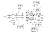
- FIG. 1 is a block diagram showing a high frequency mixer according to Embodiment 1 of the present invention.
- a differential IF terminal 1 is a terminal for inputting an IF signal with a phase of 0 ° and an IF signal with a phase of 180 ° as a differential IF signal (intermediate frequency signal).
- the differential LO terminal 2 is a terminal for inputting an LO wave having a phase of 0 ° and an LO wave having a phase of 180 ° as a differential LO wave (local signal).
- the even harmonic mixer 3 is a harmonic having a frequency that is twice the frequency of the differential IF signal input from the differential IF terminal 1 and the differential LO wave input from the differential LO terminal 2
- the second mixed wave is mixed, and a first mixed wave which is a mixed wave of an IF signal and a second harmonic of an LO wave is output from the positive phase output terminal 4, and the first mixed wave from the negative phase output terminal 5
- the positive phase output terminal 4 is a positive phase RF terminal of the even harmonic mixer 3 that outputs the first mixed wave.
- the negative phase output terminal 5 is a negative phase RF terminal of the even harmonic mixer 3 that outputs the second mixed wave.
- the first unbalanced terminal 6 is a terminal of the first balanced unbalanced circuit 7 connected to the positive phase output terminal 4 of the even harmonic mixer 3.
- the first balanced / unbalanced circuit 7 divides the first mixed wave output from the positive phase output terminal 4 of the even harmonic mixer 3 into two.
- the first balanced and unbalanced circuit 7 outputs, to the first output terminal 14, a first distributed signal that is a distributed signal in phase with the first mixed wave, of the two distributed signals of the first mixed wave.
- This is a circuit that outputs a second distribution signal, which is a distribution signal of the first mixed wave and the phase opposite to that of the first mixing wave, to the second output terminal 15.
- the first balanced positive phase terminal 8 is a terminal of the first balanced unbalanced circuit 7 connected to the first output terminal 14.
- the first balanced opposite phase terminal 9 is a terminal of the first balanced unbalanced circuit 7 connected to the second output terminal 15.
- the second unbalanced terminal 10 is a terminal of the second balanced and unbalanced circuit 11 connected to the negative phase output terminal 5 of the even harmonic mixer 3.
- the second balanced / unbalanced circuit 11 divides the second mixed wave output from the negative phase output terminal 5 of the even harmonic mixer 3 into two.
- the second balanced / unbalanced circuit 11 outputs, to the second output terminal 15, a third distributed signal of the two distributed signals of the second mixed wave, which is the distributed signal in phase with the second mixed wave. It is a circuit which outputs the 4th distribution signal which is a distribution signal of the 2nd mixed wave and reverse phase to the 1st output terminal 14.
- the second balanced positive phase terminal 12 is a terminal of the second balanced unbalanced circuit 11 connected to the second output terminal 15.
- the second balanced opposite phase terminal 13 is a terminal of the second balanced unbalanced circuit 11 connected to the first output terminal 14.
- the first output terminal 14 is connected to each of the first balanced positive phase terminal 8 of the first balanced unbalanced circuit 7 and the second balanced opposite phase terminal 13 of the second balanced unbalanced circuit 11. It is a positive phase output terminal.
- the second output terminal 15 is connected to each of the first balanced opposite phase terminal 9 of the first balanced unbalanced circuit 7 and the second balanced positive phase terminal 12 of the second balanced unbalanced circuit 11. It is a reverse phase output terminal.
- An IF signal with a phase of 0 ° and an IF signal with a phase of 180 ° are input from the differential IF terminal 1 as a differential IF signal, and a phase is 0 as a differential LO wave from the differential LO terminal 2
- An LO wave of °° and an LO wave of 180 ° in phase are input.
- the even harmonic mixer 3 mixes the differential IF signal input from the differential IF terminal 1 with the second harmonic of the differential LO wave input from the differential LO terminal 2.
- the even harmonic mixer 3 outputs a first mixed wave which is a mixed wave of an IF signal and a second harmonic of an LO wave from the positive phase output terminal 4, and outputs a first mixed wave from the negative phase output terminal 5.
- a second mixed wave which is a mixed wave of the opposite phase.
- the mixed wave of the frequency 2 f LO + f IF and the frequency 2 f LO- f IF And a mixed wave of the first and second mixed waves.
- a mixed wave having a frequency of 2f LO + f IF and a mixed wave having a frequency of 2 f LO ⁇ f IF are output from the negative phase output terminal 5 as a second mixed wave.
- the LO wave and the second harmonic of the LO wave leak from the positive phase output terminal 4 and the negative phase output terminal 5 of the even harmonic mixer 3 respectively.
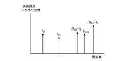
- FIG. 2 is an explanatory view showing a plurality of frequency components included in the output signal of the even harmonic mixer 3.
- the frequency f LO of the LO wave is a frequency separated from the frequency of the RF wave which is a high frequency signal as shown in FIG. 2, it can be easily cut off by a filter or the like.
- the frequency of the RF wave is a frequency such as 2f LO + f IF and 2f LO -f IF .
- the frequency 2f LO of the second harmonic of the LO wave is close to the frequency of the RF wave, it is necessary to use a filter with a steep characteristic when blocking using a filter.
- even a filter with a steep characteristic is used, it is difficult to eliminate, for example, the passing loss of the mixed wave having a frequency of 2f LO + f IF .
- phase relationship of the signals output from the positive phase output terminal 4 and the negative phase output terminal 5 of the even harmonic mixer 3 is as follows. Positive phase output terminal 4 Negative phase output terminal 5 2f LO + f IF 0 ° 180 ° 2f LO -f IF 0 ° 180 ° 2f LO 0 ° 0 °
- the first mixed wave output from the positive phase output terminal 4 of the even harmonic mixer 3 and the second mixed wave output from the negative phase output terminal 5 are in a reverse phase relationship.
- the second harmonic of the LO wave output from the positive phase output terminal 4 of the even harmonic mixer 3 and the second harmonic of the LO wave output from the negative phase output terminal 5 have an in-phase relationship.
- the phase of the first mixed wave is 0 ° and the phase of the second mixed wave is 180 °, but with the phase of the first mixed wave It is sufficient that the phase of the second mixed wave is in the opposite phase. Therefore, for example, an example may be considered in which the phase of the first mixed wave is 30 ° and the phase of the second mixed wave is 210 °.
- the first balanced / unbalanced circuit 7 divides the first mixed wave output from the positive phase output terminal 4 of the even harmonic mixer 3 into two.
- the first balanced and unbalanced circuit 7 is a first split signal that is a split signal in phase with the first mixing wave from the first balanced positive phase terminal 8 among the two split signals of the first mixing wave. Are output to the first output terminal 14. Further, the first balanced / unbalanced circuit 7 outputs, from the first balanced opposite phase terminal 9, a second divided signal which is a divided signal of the first mixed wave and the opposite phase to the second output terminal 15. .
- the second distribution signal is a signal obtained by shifting the phase of the distribution signal of one of the two distribution signals of the first mixing wave that is not the first distribution signal by 180 °, and the first distribution signal It is a distribution signal of reverse phase.
- the phase relationship of the signals output from the first balanced positive phase terminal 8 and the first balanced opposite phase terminal 9 of the first balanced unbalanced circuit 7 is as follows. First balanced positive phase terminal 8 First balanced negative phase terminal 9 2f LO + f IF 0 ° 180 ° 2f LO -f IF 0 ° 180 ° 2f LO 0 ° 180 °
- the second balanced / unbalanced circuit 11 divides the second mixed wave output from the negative phase output terminal 5 of the even harmonic mixer 3 into two.
- the second balanced / unbalanced circuit 11 is a third split signal that is a split signal in phase with the second mixed wave from the second balanced positive phase terminal 12 among the two split signals of the second mixed wave. Are output to the second output terminal 15. Further, the second balanced / unbalanced circuit 11 outputs, from the second balanced opposite phase terminal 13, a fourth divided signal, which is a distributed signal of the second mixed wave and the opposite phase, to the first output terminal 14. .
- the fourth distribution signal is a signal obtained by shifting the phase of the distribution signal other than the third distribution signal among the two distribution signals of the second mixing wave by 180 °, and is the third distribution signal It is a distribution signal of reverse phase.
- the phase relationship of the signals output from the second balanced positive phase terminal 12 and the second balanced negative phase terminal 13 of the second balanced unbalanced circuit 11 is as follows. Second balanced positive phase terminal 12 Second balanced negative phase terminal 13 2f LO + f IF 180 ° 0 ° 2f LO -f IF 180 ° 0 ° 2f LO 0 ° 180 °
- the signal of frequency 2f LO + f IF and the signal of frequency 2f LO -f IF outputted from the balanced reverse phase terminal 13 of the first phase are both in-phase signals of 0 ° in phase. Therefore, a signal of frequency 2f LO + f IF with a phase of 0 ° and a signal of frequency 2f LO -f IF with a phase of 0 ° are output from the first output terminal 14.
- a frequency 2f LO + f IF of the signal and the frequency 2f LO -f IF of the signal output from the first balanced anti-phase terminal 9 of the first balanced-unbalanced circuit 7, the second balun circuit 11 The signal of frequency 2f LO + f IF and the signal of frequency 2 f LO ⁇ f IF outputted from the second balanced positive phase terminal 12 are both in-phase signals of 180 ° in phase. Therefore, a signal of frequency 2f LO + f IF with a phase of 180 ° and a signal of frequency 2 f LO -f IF with a phase of 180 ° are output from the second output terminal 15. Therefore, the first output terminal 14 and the second output terminal 15 output differential signals that are a set of signals that are 180 ° out of phase with each other.
- the second harmonic of the frequency 2f LO is a signal with an opposite phase that is 180 ° out of phase. Therefore, the second harmonic frequency 2f LO output from the first balanced positive phase terminal 8 and the second harmonic frequency 2f LO output from the second balanced anti-phase terminal 13, a first output The terminal 14 is offset. Therefore, the second harmonic of the frequency 2f LO is not output from the first output terminal 14.
- the second harmonic of the frequency 2f LO is a signal with an opposite phase that is 180 ° out of phase. Therefore, the second harmonic of the frequency 2f LO output from the first balanced opposite phase terminal 9 and the second harmonic of the frequency 2f LO output from the second balanced positive phase terminal 12 have the second output.
- the terminal 15 is offset. Therefore, the second harmonic of the frequency 2f LO is not output from the second output terminal 15.
- the first mixed wave output from the even harmonic mixer 3 is divided into two, and of the two divided signals of the first mixed wave,
- a first distribution signal which is a distribution signal in phase with the first mixing wave, is output to the first output terminal 14, and a second distribution signal, which is a distribution signal in reverse phase to the first mixing wave, is output as a second distribution signal.
- the first balanced / unbalanced circuit 7 outputting to the output terminal 15 and the second mixed wave output from the even harmonic mixer 3 are divided into two, and of the two divided signals of the second mixed wave, A third distribution signal, which is a distribution signal in phase with the second mixing wave, is output to the second output terminal 15, and a fourth distribution signal, which is a distribution signal in reverse phase to the second mixing wave, is output as a first distribution signal. And a second balanced / unbalanced circuit 11 that outputs to the output terminal 14. As a result, the differential signal can be output without causing the passage loss associated with the removal of the unnecessary wave.
- the high frequency mixer includes the first balanced unbalance circuit 7 and the second balanced unbalance circuit 11 is shown.
- the first balanced unbalanced circuit 7 is a first merchant balun and the second balanced unbalanced circuit 11 is a second merchant balun.
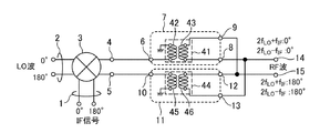
- FIG. 3 is a block diagram showing a high frequency mixer according to a second embodiment of the present invention.
- the first balanced and unbalanced circuit 7 which is a first merchant balun includes transmission lines 21, 22 and 23.
- the first balanced / unbalanced circuit 7, which is the first merchant balun divides the first mixed wave output from the even harmonic mixer 3 into two, and
- the first distribution signal which is the distribution signal in phase with the first mixing wave, of the two distribution signals of the mixing wave is outputted to the first output terminal 14, and the distribution signal of the phase opposite to the first mixing wave is output.
- a second distributed signal is output to the second output terminal 15.
- the transmission line 21 of the first merchant balun has one end connected to the first unbalanced terminal 6 and the other end opened, and the half wave length at the frequency 2f LO of the double wave.
- Is a line having The transmission line 22 of the first merchant balun has one end connected to the first balanced positive phase terminal 8 and the other end grounded, and is adjacently arranged parallel to the transmission line 21.
- the transmission line 22 is a line having a length of a quarter wavelength at a frequency 2f LO of a double wave.
- the transmission line 23 of the first merchant balun has one end connected to the first balanced opposite phase terminal 9 and the other end grounded, and is adjacently arranged in parallel with the transmission line 21. Further, the transmission line 23 is a line having a length of 1 ⁇ 4 wavelength at a frequency 2f LO of a double wave.
- the second balanced / unbalanced circuit 11, which is a second merchant balun, includes transmission lines 24, 25, 26.
- the second balanced / unbalanced circuit 11 which is the second merchant balun includes two second mixed waves output from the negative phase output terminal 5 of the even harmonic mixer 3. And, of the two distribution signals of the second mixing wave, the third distribution signal that is the distribution signal in phase with the second mixing wave is output to the second output terminal 15, and the second mixing wave A fourth distribution signal which is a distribution signal of reverse phase is output to the first output terminal 14.
- the transmission line 24 of the second merchant balun has one end connected to the second unbalanced terminal 10 and the other end opened, and a half wavelength length at a frequency 2f LO of a double wave.
- the transmission line 25 of the second merchant balun has one end connected to the second balanced positive phase terminal 12 and the other end grounded, and is adjacently arranged parallel to the transmission line 24. Further, the transmission line 25 is a line having a length of a quarter wavelength at a frequency 2f LO of a double wave.
- the transmission line 26 of the second merchant balun has one end connected to the second balanced opposite phase terminal 13 and the other end grounded, and is adjacently arranged in parallel with the transmission line 24. Further, the transmission line 26 is a line having a length of a quarter wavelength at a frequency 2f LO of a double wave.
- the first Marchant balun is used as the first balanced unbalance circuit 7, and the second Marchant balun is used as the second balanced unbalance circuit 11.
- the first merchant balun and the second merchant balun are known as broadband balanced-to-unbalanced conversion circuits. Therefore, each of the first merchant balun and the second merchant balun can suppress unnecessary waves other than the second harmonic of the LO wave output from the even harmonic mixer 3. For example, it is also possible to suppress LO waves and third harmonics whose frequency is 3f LO .
- the differential signal can be output without causing the passage loss associated with the removal of the unnecessary wave, and the unnecessary wave other than the double wave can be suppressed. it can.
- FIG. 4 is a block diagram showing a high frequency mixer according to a third embodiment of the present invention.
- the same reference numerals as those in FIG. 1 denote the same or corresponding parts, and the description thereof will be omitted.
- the first balanced and unbalanced circuit 7 includes a first in-phase distributor 31, a first transmission line 32 and a second transmission line 33.
- the first in-phase distributor 31 is connected to the first unbalanced terminal 6 and distributes the first mixed wave output from the positive phase output terminal 4 of the even harmonic mixer 3 in phase.
- the first transmission line 32 has one end connected to the first in-phase distributor 31 and the other end connected to the first balanced positive-phase terminal 8, and is in-phase distributed by the first in-phase distributor 31. It is a line that propagates one first mixed wave.
- the second transmission line 33 has one end connected to the first in-phase distributor 31 and the other end connected to the first balanced opposite phase terminal 9, and is in-phase distributed by the first in-phase distributor 31. It is a line that propagates the other first mixed wave.
- the second transmission line 33 has a line length longer than that of the first transmission line 32 by the half wave length at the frequency 2f LO of the double wave.
- the second balanced / unbalanced circuit 11 includes a second in-phase distributor 34, a third transmission line 35, and a fourth transmission line 36.
- the second in-phase distributor 34 is connected to the second unbalanced terminal 10 and distributes in phase the second mixed wave output from the negative phase output terminal 5 of the even harmonic mixer 3.
- the third transmission line 35 has one end connected to the second in-phase distributor 34 and the other end connected to the second balanced positive phase terminal 12, and is in-phase distributed by the second in-phase distributor 34. It is a line that propagates one second mixed wave.
- the fourth transmission line 36 has one end connected to the second in-phase distributor 34 and the other end connected to the second balanced opposite phase terminal 13, and is in-phase distributed by the second in-phase distributor 34.
- the fourth transmission line 36 has a line length longer than that of the third transmission line 35 by a half wavelength at the frequency 2f LO of the double wave.
- the first transmission line 32 and the third transmission line 35 have the same length.
- the first in-phase splitter 31 of the first balanced / unbalanced circuit 7 splits in phase the first mixed wave output from the positive phase output terminal 4 of the even harmonic mixer 3 and splits the first mixed wave in phase
- the second mixed wave is output to the first transmission line 32, and the other first mixed wave subjected to the in-phase distribution is output to the second transmission line 33.
- the second transmission line 33 of the first balanced and unbalanced circuit 7 has a line length longer than that of the first transmission line 32 by a half wavelength at the frequency 2f LO of the second harmonic. . For this reason, the phase of the signal propagated through the second transmission line 33 and output from the first balanced opposite phase terminal 9 is propagated through the first transmission line 32 to form the first balanced positive phase terminal 8. It is 180 degrees behind the phase of the signal output from.
- the second in-phase splitter 34 of the second balanced / unbalanced circuit 11 splits in phase the second mixed wave output from the negative phase output terminal 5 of the even harmonic mixer 3 and splits the second mixed wave in phase
- the second mixed wave of the in-phase distribution is output to the fourth transmission line 36.
- the fourth transmission line 36 of the second balanced / unbalanced circuit 11 has a line length longer than that of the third transmission line 35 by a half wavelength at the frequency 2f LO of the second harmonic. . Therefore, the phase of the signal transmitted through the fourth transmission line 36 and output from the second balanced opposite phase terminal 13 is propagated through the third transmission line 35, and the second balanced positive phase terminal 12 is transmitted. It is 180 degrees behind the phase of the signal output from.
- the phase difference between the two first mixed waves output from the first in-phase distributor 31 is originally 0 °, but even if the phase difference between the two first mixed waves is deviated from 0 °,
- the phase difference with the signal can be 180 °.
- the phase difference between the two second mixed waves output from the second in-phase distributor 34 is originally 0 °, the phase difference between the two second mixed waves is deviated from 0 °.
- the signal output from the second balanced positive phase terminal 12 and the second balanced negative phase terminal 13 can be obtained.
- the phase difference with the output signal can be made 180 °.
- the differential signal can be output without causing the passage loss accompanying the removal of the unnecessary wave.
- the amount of suppression of the second harmonic of the LO wave depends on the phase accuracy of the first unbalance circuit 7 and the second unbalance circuit 11.
- FIG. 5 is a block diagram showing a high frequency mixer according to a fourth embodiment of the present invention.
- the same reference numerals as those in FIG. 5 are identical reference numerals as those in FIG. 5.
- the first balanced and unbalanced circuit 7 includes the first transformer 41
- the second balanced and unbalanced circuit 11 includes the second transformer 44.
- the first transformer 41 includes a first spiral line 42 and a second spiral line 43.
- the first spiral line 42 is a spiral line whose one end is connected to the first unbalanced terminal 6 and the other end is grounded.
- One end of the second spiral line 43 is connected to the first balanced positive phase terminal 8 and the other end is connected to the first balanced negative phase terminal 9, and the second spiral line 43 is connected to the first spiral line 42. It is a spiral-shaped line that induces electromagnetic induction.
- the second transformer 44 includes a third spiral line 45 and a fourth spiral line 46.
- the third spiral line 45 is a spiral line whose one end is connected to the second unbalanced terminal 10 and the other end is grounded.
- the fourth spiral line 46 has one end connected to the second balanced positive phase terminal 12 and the other end connected to the second balanced negative phase terminal 13, and the fourth spiral line 46 is connected to the third spiral line 45. It is a spiral-shaped line that induces electromagnetic induction.
- the first transformer 41 is formed by arranging the first spiral line 42 and the second spiral line 43, which are spiral-shaped lines, on the dielectric substrate. Be done.
- the second transformer 44 is also formed by arranging the third spiral line 45 and the fourth spiral line 46, which are spiral-shaped lines, on the dielectric substrate as shown in FIG.
- FIG. 6 is an explanatory view showing an example of the first transformer 41 and the second transformer 44. As shown in FIG. Although FIG. 6 shows an example in which the number of turns of each of the first transformer 41 and the second transformer 44 is one, increasing the number of turns strengthens the coupling of the two spiral lines, The size of the first transformer 41 and the second transformer 44 can be reduced.
- the first balanced unbalanced circuit 7 and the second balanced unbalanced circuit 11 include transmission lines, and at least a half wavelength of the second harmonic wave frequency 2f LO .
- the length is necessary. For this reason, it is necessary to secure at least an area for mounting a transmission line having a length of a half wavelength at frequency 2f LO .
- the first spiral line 42 and the second spiral line 43 in the first transformer 41 are spiral-shaped lines, and the third spiral line 45 in the second transformer 44 and the third spiral line 45
- the fourth spiral line 46 is a spiral line. Therefore, the mounting area can be made smaller than in the second and third embodiments. Further, in the fourth embodiment, as in the first embodiment, it is possible to output a differential signal without causing a passage loss accompanying the removal of the unnecessary wave.
- the present invention allows free combination of each embodiment, or modification of any component of each embodiment, or omission of any component in each embodiment. .
- the invention is suitable for high frequency mixers comprising even harmonic mixers that mix an intermediate frequency signal with harmonics having a frequency twice that of the local signal.
Landscapes
- Engineering & Computer Science (AREA)
- Power Engineering (AREA)
- Superheterodyne Receivers (AREA)
Abstract
偶高調波ミクサ(3)から出力された第1の混合波を2つに分配し、第1の混合波の2つの分配信号のうち、第1の混合波と同相の分配信号である第1の分配信号を第1の出力端子(14)に出力し、第1の混合波と逆相の分配信号である第2の分配信号を第2の出力端子(15)に出力する第1の平衡不平衡回路(7)と、偶高調波ミクサ(3)から出力された第2の混合波を2つに分配し、第2の混合波の2つの分配信号のうち、第2の混合波と同相の分配信号である第3の分配信号を第2の出力端子(15)に出力し、第2の混合波と逆相の分配信号である第4の分配信号を第1の出力端子(14)に出力する第2の平衡不平衡回路(11)とを備える。
Description
この発明は、中間周波数信号と、ローカル信号の周波数の2倍の周波数を有する高調波とを混合する偶高調波ミクサを備える高周波ミクサに関するものである。
例えば、マイクロ波又はミリ波帯の無線装置の周波数変換部に用いるコンポーネントとして、高周波ミクサがある。
無線装置の低コスト化及び周波数安定度の改善などを図るには、ローカル信号であるLO波の低周波化が求められる。
このため、LO波の周波数の2倍の周波数を有する高調波である2倍波と、中間周波数信号であるIF信号との混合波を生成する偶高調波ミクサを用いることがある。
高周波ミクサが偶高調波ミクサを用いる場合、LO波とIF信号を混合する高周波ミクサと比べて、LO波の周波数を2分の1にすることができる。
無線装置の低コスト化及び周波数安定度の改善などを図るには、ローカル信号であるLO波の低周波化が求められる。
このため、LO波の周波数の2倍の周波数を有する高調波である2倍波と、中間周波数信号であるIF信号との混合波を生成する偶高調波ミクサを用いることがある。
高周波ミクサが偶高調波ミクサを用いる場合、LO波とIF信号を混合する高周波ミクサと比べて、LO波の周波数を2分の1にすることができる。
以下の特許文献1に開示されている偶高調波ミクサは、以下に示す3つのトランジスタを備える単位ミクサが、2つ並列に配置されているものである。
(1)コレクタ端子が出力負荷を介して電源に接続されている第1のNPNトランジスタ
(2)コレクタ端子が第1のNPNトランジスタのコレクタ端子と接続され、エミッタ端子が第1のNPNトランジスタのエミッタ端子と接続されている第2のNPNトランジスタ
(3)コレクタ端子が第1及び第2のNPNトランジスタのエミッタ端子と接続され、エミッタ端子がグランドと接続されている第3のNPNトランジスタ
(1)コレクタ端子が出力負荷を介して電源に接続されている第1のNPNトランジスタ
(2)コレクタ端子が第1のNPNトランジスタのコレクタ端子と接続され、エミッタ端子が第1のNPNトランジスタのエミッタ端子と接続されている第2のNPNトランジスタ
(3)コレクタ端子が第1及び第2のNPNトランジスタのエミッタ端子と接続され、エミッタ端子がグランドと接続されている第3のNPNトランジスタ
この偶高調波ミクサでは、差動のLO波が入力される差動LO入力端子が、各々の単位ミクサの第1及び第2のNPNトランジスタのベース端子に接続され、差動のIF信号が入力される差動IF入力端子が、第3のNPNトランジスタのベース端子に接続されている。
このため、差動LO入力端子から入力されたLO波の2倍波と、差動IF入力端子から入力されたIF信号とが混合された混合波が、第1及び第2のNPNトランジスタのコレクタ端子から出力される。これにより、第1及び第2のNPNトランジスタのコレクタ端子と接続されている出力端子から、当該混合波が出力される。
LO波の周波数がfLO、IF信号の周波数がfIFであれば、第1及び第2のNPNトランジスタのコレクタ端子と接続されている出力端子から、周波数が2fLO+fIFの混合波と、周波数が2fLO-fIFの混合波とが出力される。
このため、差動LO入力端子から入力されたLO波の2倍波と、差動IF入力端子から入力されたIF信号とが混合された混合波が、第1及び第2のNPNトランジスタのコレクタ端子から出力される。これにより、第1及び第2のNPNトランジスタのコレクタ端子と接続されている出力端子から、当該混合波が出力される。
LO波の周波数がfLO、IF信号の周波数がfIFであれば、第1及び第2のNPNトランジスタのコレクタ端子と接続されている出力端子から、周波数が2fLO+fIFの混合波と、周波数が2fLO-fIFの混合波とが出力される。
一方の単位ミクサの出力端子から出力される周波数が2fLO+fIFの混合波と、他方の単位ミクサの出力端子から出力される周波数が2fLO-fIFの混合波とは、位相が反転している。このため、周波数が2fLO+fIFの混合波と、周波数が2fLO-fIFの混合波とは、差動信号である。
また、一方の単位ミクサの出力端子からは、周波数が2fLO+fIFの混合波のほかに、周波数が2fLOの信号としてLO波の2倍波が出力され、他方の単位ミクサの出力端子からは、周波数が2fLO-fIFの混合波のほかに、LO波の2倍波が出力される。
一方の単位ミクサの出力端子から出力されるLO波の2倍波と、他方の単位ミクサの出力端子から出力されるLO波の2倍波とは、同相信号である。
また、一方の単位ミクサの出力端子からは、周波数が2fLO+fIFの混合波のほかに、周波数が2fLOの信号としてLO波の2倍波が出力され、他方の単位ミクサの出力端子からは、周波数が2fLO-fIFの混合波のほかに、LO波の2倍波が出力される。
一方の単位ミクサの出力端子から出力されるLO波の2倍波と、他方の単位ミクサの出力端子から出力されるLO波の2倍波とは、同相信号である。
周波数が2fLO+fIFの混合波及び周波数が2fLO-fIFの混合波のうち、例えば、周波数が2fLO+fIFの混合波が所望の信号である場合、周波数が2fLO-fIFの混合波及びLO波の2倍波は、不要波である。
周波数が2fLO-fIFの混合波及びLO波の2倍波を除去するには、偶高調波ミクサの後段にフィルタを設ければよいが、LO波の2倍波は、所望の信号である周波数が2fLO+fIFの混合波と周波数が近いため、LO波の2倍波を除去するには、急峻な特性のフィルタが必要である。
周波数が2fLO-fIFの混合波及びLO波の2倍波を除去するには、偶高調波ミクサの後段にフィルタを設ければよいが、LO波の2倍波は、所望の信号である周波数が2fLO+fIFの混合波と周波数が近いため、LO波の2倍波を除去するには、急峻な特性のフィルタが必要である。
従来の偶高調波ミクサは、後段に急峻な特性のフィルタを設ければ、不要波であるLO波の2倍波を除去する際、所望の信号である周波数が2fLO+fIFの混合波の通過損失を抑えることができる。しかし、急峻な特性のフィルタを用いても、所望の信号である周波数が2fLO+fIFの混合波の通過損失を無くすことは困難である。
また、不要波であるLO波の2倍波を除去する際に、周波数が2fLO-fIFの混合波も不要波として除去されてしまう。
このため、周波数が2fLO+fIFの混合波と、周波数が2fLO-fIFの混合波とを差動信号として出力することができないという課題があった。
また、不要波であるLO波の2倍波を除去する際に、周波数が2fLO-fIFの混合波も不要波として除去されてしまう。
このため、周波数が2fLO+fIFの混合波と、周波数が2fLO-fIFの混合波とを差動信号として出力することができないという課題があった。
この発明は上記のような課題を解決するためになされたもので、不要波の除去に伴う通過損失を招くことなく、差動信号を出力することができる高周波ミクサを得ることを目的とする。
この発明に係る高周波ミクサは、差動の中間周波数信号と、差動のローカル信号の周波数の2倍の周波数を有する高調波とを混合して、中間周波数信号と高調波との混合波である第1の混合波を出力し、第1の混合波と逆相の混合波である第2の混合波を出力する偶高調波ミクサと、偶高調波ミクサから出力された第1の混合波を2つに分配し、第1の混合波の2つの分配信号のうち、第1の混合波と同相の分配信号である第1の分配信号を第1の出力端子に出力し、第1の混合波と逆相の分配信号である第2の分配信号を第2の出力端子に出力する第1の平衡不平衡回路と、偶高調波ミクサから出力された第2の混合波を2つに分配し、第2の混合波の2つの分配信号のうち、第2の混合波と同相の分配信号である第3の分配信号を第2の出力端子に出力し、第2の混合波と逆相の分配信号である第4の分配信号を第1の出力端子に出力する第2の平衡不平衡回路とを備えるようにしたものである。
この発明によれば、偶高調波ミクサから出力された第1の混合波を2つに分配し、第1の混合波の2つの分配信号のうち、第1の混合波と同相の分配信号である第1の分配信号を第1の出力端子に出力し、第1の混合波と逆相の分配信号である第2の分配信号を第2の出力端子に出力する第1の平衡不平衡回路と、偶高調波ミクサから出力された第2の混合波を2つに分配し、第2の混合波の2つの分配信号のうち、第2の混合波と同相の分配信号である第3の分配信号を第2の出力端子に出力し、第2の混合波と逆相の分配信号である第4の分配信号を第1の出力端子に出力する第2の平衡不平衡回路とを備えるように構成したので、不要波の除去に伴う通過損失を招くことなく、差動信号を出力することができる効果がある。
以下、この発明をより詳細に説明するために、この発明を実施するための形態について、添付の図面に従って説明する。
実施の形態1.
図1は、この発明の実施の形態1による高周波ミクサを示す構成図である。
図1において、差動IF端子1は、差動のIF信号(中間周波数信号)として、位相が0°のIF信号と、位相が180°のIF信号とを入力する端子である。
差動LO端子2は、差動のLO波(ローカル信号)として、位相が0°のLO波と、位相が180°のLO波とを入力する端子である。
偶高調波ミクサ3は、差動IF端子1から入力された差動のIF信号と、差動LO端子2から入力された差動のLO波の周波数の2倍の周波数を有する高調波である2倍波とを混合し、正相出力端子4から、IF信号とLO波の2倍波との混合波である第1の混合波を出力し、逆相出力端子5から、第1の混合波と逆相の混合波である第2の混合波を出力する。
正相出力端子4は、第1の混合波を出力する偶高調波ミクサ3の正相RF端子である。
逆相出力端子5は、第2の混合波を出力する偶高調波ミクサ3の逆相RF端子である。
第1の不平衡端子6は、偶高調波ミクサ3の正相出力端子4と接続されている第1の平衡不平衡回路7の端子である。
第1の平衡不平衡回路7は、偶高調波ミクサ3の正相出力端子4から出力された第1の混合波を2つに分配する。
第1の平衡不平衡回路7は、第1の混合波の2つの分配信号のうち、第1の混合波と同相の分配信号である第1の分配信号を第1の出力端子14に出力し、第1の混合波と逆相の分配信号である第2の分配信号を第2の出力端子15に出力する回路である。
第1の平衡正相端子8は、第1の出力端子14と接続されている第1の平衡不平衡回路7の端子である。
第1の平衡逆相端子9は、第2の出力端子15と接続されている第1の平衡不平衡回路7の端子である。
第1の平衡不平衡回路7は、偶高調波ミクサ3の正相出力端子4から出力された第1の混合波を2つに分配する。
第1の平衡不平衡回路7は、第1の混合波の2つの分配信号のうち、第1の混合波と同相の分配信号である第1の分配信号を第1の出力端子14に出力し、第1の混合波と逆相の分配信号である第2の分配信号を第2の出力端子15に出力する回路である。
第1の平衡正相端子8は、第1の出力端子14と接続されている第1の平衡不平衡回路7の端子である。
第1の平衡逆相端子9は、第2の出力端子15と接続されている第1の平衡不平衡回路7の端子である。
第2の不平衡端子10は、偶高調波ミクサ3の逆相出力端子5と接続されている第2の平衡不平衡回路11の端子である。
第2の平衡不平衡回路11は、偶高調波ミクサ3の逆相出力端子5から出力された第2の混合波を2つに分配する。
第2の平衡不平衡回路11は、第2の混合波の2つの分配信号のうち、第2の混合波と同相の分配信号である第3の分配信号を第2の出力端子15に出力し、第2の混合波と逆相の分配信号である第4の分配信号を第1の出力端子14に出力する回路である。
第2の平衡正相端子12は、第2の出力端子15と接続されている第2の平衡不平衡回路11の端子である。
第2の平衡逆相端子13は、第1の出力端子14と接続されている第2の平衡不平衡回路11の端子である。
第2の平衡不平衡回路11は、偶高調波ミクサ3の逆相出力端子5から出力された第2の混合波を2つに分配する。
第2の平衡不平衡回路11は、第2の混合波の2つの分配信号のうち、第2の混合波と同相の分配信号である第3の分配信号を第2の出力端子15に出力し、第2の混合波と逆相の分配信号である第4の分配信号を第1の出力端子14に出力する回路である。
第2の平衡正相端子12は、第2の出力端子15と接続されている第2の平衡不平衡回路11の端子である。
第2の平衡逆相端子13は、第1の出力端子14と接続されている第2の平衡不平衡回路11の端子である。
第1の出力端子14は、第1の平衡不平衡回路7の第1の平衡正相端子8及び第2の平衡不平衡回路11の第2の平衡逆相端子13のそれぞれと接続されている正相出力端子である。
第2の出力端子15は、第1の平衡不平衡回路7の第1の平衡逆相端子9及び第2の平衡不平衡回路11の第2の平衡正相端子12のそれぞれと接続されている逆相出力端子である。
第2の出力端子15は、第1の平衡不平衡回路7の第1の平衡逆相端子9及び第2の平衡不平衡回路11の第2の平衡正相端子12のそれぞれと接続されている逆相出力端子である。
次に動作について説明する。
差動IF端子1から差動のIF信号として、位相が0°のIF信号と、位相が180°のIF信号とが入力され、差動LO端子2から差動のLO波として、位相が0°のLO波と、位相が180°のLO波とが入力される。
偶高調波ミクサ3は、差動IF端子1から入力された差動のIF信号と、差動LO端子2から入力された差動のLO波の2倍波とを混合する。
偶高調波ミクサ3は、正相出力端子4から、IF信号とLO波の2倍波との混合波である第1の混合波を出力し、逆相出力端子5から、第1の混合波と逆相の混合波である第2の混合波を出力する。
差動IF端子1から差動のIF信号として、位相が0°のIF信号と、位相が180°のIF信号とが入力され、差動LO端子2から差動のLO波として、位相が0°のLO波と、位相が180°のLO波とが入力される。
偶高調波ミクサ3は、差動IF端子1から入力された差動のIF信号と、差動LO端子2から入力された差動のLO波の2倍波とを混合する。
偶高調波ミクサ3は、正相出力端子4から、IF信号とLO波の2倍波との混合波である第1の混合波を出力し、逆相出力端子5から、第1の混合波と逆相の混合波である第2の混合波を出力する。
LO波の周波数がfLO、IF信号の周波数がfIFであれば、偶高調波ミクサ3の正相出力端子4から、周波数が2fLO+fIFの混合波と、周波数が2fLO-fIFの混合波とが第1の混合波として出力される。
また、逆相出力端子5から、周波数が2fLO+fIFの混合波と、周波数が2fLO-fIFの混合波とが第2の混合波として出力される。
また、偶高調波ミクサ3の正相出力端子4及び逆相出力端子5から、LO波及びLO波の2倍波のそれぞれが漏洩する。
また、逆相出力端子5から、周波数が2fLO+fIFの混合波と、周波数が2fLO-fIFの混合波とが第2の混合波として出力される。
また、偶高調波ミクサ3の正相出力端子4及び逆相出力端子5から、LO波及びLO波の2倍波のそれぞれが漏洩する。
図2は、偶高調波ミクサ3の出力信号に含まれている複数の周波数成分を示す説明図である。
LO波の周波数fLOは、図2に示すように、高周波信号であるRF波の周波数から離れた周波数であるため、フィルタ等で容易に遮断することが可能である。RF波の周波数は、2fLO+fIF,2fLO-fIFなどの周波数である。
しかし、LO波の2倍波の周波数2fLOは、RF波の周波数と近接しているため、フィルタを用いて遮断する場合には、急峻な特性のフィルタを用いる必要がある。ただし、急峻な特性のフィルタを用いても、例えば、周波数が2fLO+fIFの混合波の通過損失を無くすことは困難である。
LO波の周波数fLOは、図2に示すように、高周波信号であるRF波の周波数から離れた周波数であるため、フィルタ等で容易に遮断することが可能である。RF波の周波数は、2fLO+fIF,2fLO-fIFなどの周波数である。
しかし、LO波の2倍波の周波数2fLOは、RF波の周波数と近接しているため、フィルタを用いて遮断する場合には、急峻な特性のフィルタを用いる必要がある。ただし、急峻な特性のフィルタを用いても、例えば、周波数が2fLO+fIFの混合波の通過損失を無くすことは困難である。
偶高調波ミクサ3の正相出力端子4及び逆相出力端子5から出力される信号の位相関係は、以下の通りである。
正相出力端子4 逆相出力端子5
2fLO+fIF 0° 180°
2fLO-fIF 0° 180°
2fLO 0° 0°
正相出力端子4 逆相出力端子5
2fLO+fIF 0° 180°
2fLO-fIF 0° 180°
2fLO 0° 0°
したがって、偶高調波ミクサ3の正相出力端子4から出力される第1の混合波と、逆相出力端子5から出力される第2の混合波とは、逆相の関係にある。
また、偶高調波ミクサ3の正相出力端子4から出力されるLO波の2倍波と、逆相出力端子5から出力されるLO波の2倍波とは、同相の関係にある。
ここでは、説明の簡単化のために、第1の混合波の位相が0°で、第2の混合波の位相が180°である例を示しているが、第1の混合波の位相と第2の混合波の位相とが逆相の関係であればよい。
したがって、例えば、第1の混合波の位相が30°で、第2の混合波の位相が210°である例も考えられる。
また、偶高調波ミクサ3の正相出力端子4から出力されるLO波の2倍波と、逆相出力端子5から出力されるLO波の2倍波とは、同相の関係にある。
ここでは、説明の簡単化のために、第1の混合波の位相が0°で、第2の混合波の位相が180°である例を示しているが、第1の混合波の位相と第2の混合波の位相とが逆相の関係であればよい。
したがって、例えば、第1の混合波の位相が30°で、第2の混合波の位相が210°である例も考えられる。
第1の平衡不平衡回路7は、偶高調波ミクサ3の正相出力端子4から出力された第1の混合波を2つに分配する。
第1の平衡不平衡回路7は、第1の混合波の2つの分配信号のうち、第1の平衡正相端子8から、第1の混合波と同相の分配信号である第1の分配信号を第1の出力端子14に出力する。
また、第1の平衡不平衡回路7は、第1の平衡逆相端子9から、第1の混合波と逆相の分配信号である第2の分配信号を第2の出力端子15に出力する。
第2の分配信号は、第1の混合波の2つの分配信号のうち、第1の分配信号ではない方の分配信号の位相を180°移相した信号であり、第1の分配信号とは逆相の分配信号である。
第1の平衡不平衡回路7の第1の平衡正相端子8及び第1の平衡逆相端子9から出力される信号の位相関係は、以下の通りである。
第1の平衡正相端子8 第1の平衡逆相端子9
2fLO+fIF 0° 180°
2fLO-fIF 0° 180°
2fLO 0° 180°
第2の平衡不平衡回路11は、偶高調波ミクサ3の逆相出力端子5から出力された第2の混合波を2つに分配する。
第2の平衡不平衡回路11は、第2の混合波の2つの分配信号のうち、第2の平衡正相端子12から、第2の混合波と同相の分配信号である第3の分配信号を第2の出力端子15に出力する。
また、第2の平衡不平衡回路11は、第2の平衡逆相端子13から、第2の混合波と逆相の分配信号である第4の分配信号を第1の出力端子14に出力する。
第4の分配信号は、第2の混合波の2つの分配信号のうち、第3の分配信号ではない方の分配信号の位相を180°移相した信号であり、第3の分配信号とは逆相の分配信号である。
第2の平衡不平衡回路11の第2の平衡正相端子12及び第2の平衡逆相端子13から出力される信号の位相関係は、以下の通りである。
第2の平衡正相端子12 第2の平衡逆相端子13
2fLO+fIF 180° 0°
2fLO-fIF 180° 0°
2fLO 0° 180°
第1の平衡不平衡回路7の第1の平衡正相端子8から出力される周波数2fLO+fIFの信号及び周波数2fLO-fIFの信号と、第2の平衡不平衡回路11の第2の平衡逆相端子13から出力される周波数2fLO+fIFの信号及び周波数2fLO-fIFの信号とは、共に位相が0°の同相信号である。
したがって、第1の出力端子14から、位相が0°の周波数2fLO+fIFの信号及び位相が0°の周波数2fLO-fIFの信号が出力される。
したがって、第1の出力端子14から、位相が0°の周波数2fLO+fIFの信号及び位相が0°の周波数2fLO-fIFの信号が出力される。
また、第1の平衡不平衡回路7の第1の平衡逆相端子9から出力される周波数2fLO+fIFの信号及び周波数2fLO-fIFの信号と、第2の平衡不平衡回路11の第2の平衡正相端子12から出力される周波数2fLO+fIFの信号及び周波数2fLO-fIFの信号とは、共に位相が180°の同相信号である。
したがって、第2の出力端子15から、位相が180°の周波数2fLO+fIFの信号及び位相が180°の周波数2fLO-fIFの信号が出力される。
よって、第1の出力端子14及び第2の出力端子15から、互いの位相が180°異なる信号の組である差動信号が出力される。
したがって、第2の出力端子15から、位相が180°の周波数2fLO+fIFの信号及び位相が180°の周波数2fLO-fIFの信号が出力される。
よって、第1の出力端子14及び第2の出力端子15から、互いの位相が180°異なる信号の組である差動信号が出力される。
第1の平衡不平衡回路7の第1の平衡正相端子8から出力される周波数2fLOの2倍波と、第2の平衡不平衡回路11の第2の平衡逆相端子13から出力される周波数2fLOの2倍波とは、位相が180°異なる逆相の信号である。
このため、第1の平衡正相端子8から出力される周波数2fLOの2倍波と、第2の平衡逆相端子13から出力される周波数2fLOの2倍波とは、第1の出力端子14において、相殺される。このため、第1の出力端子14から周波数2fLOの2倍波は出力されない。
このため、第1の平衡正相端子8から出力される周波数2fLOの2倍波と、第2の平衡逆相端子13から出力される周波数2fLOの2倍波とは、第1の出力端子14において、相殺される。このため、第1の出力端子14から周波数2fLOの2倍波は出力されない。
第1の平衡不平衡回路7の第1の平衡逆相端子9から出力される周波数2fLOの2倍波と、第2の平衡不平衡回路11の第2の平衡正相端子12から出力される周波数2fLOの2倍波とは、位相が180°異なる逆相の信号である。
このため、第1の平衡逆相端子9から出力される周波数2fLOの2倍波と、第2の平衡正相端子12から出力される周波数2fLOの2倍波とは、第2の出力端子15において、相殺される。このため、第2の出力端子15から周波数2fLOの2倍波は出力されない。
このため、第1の平衡逆相端子9から出力される周波数2fLOの2倍波と、第2の平衡正相端子12から出力される周波数2fLOの2倍波とは、第2の出力端子15において、相殺される。このため、第2の出力端子15から周波数2fLOの2倍波は出力されない。
以上で明らかなように、この実施の形態1によれば、偶高調波ミクサ3から出力された第1の混合波を2つに分配し、第1の混合波の2つの分配信号のうち、第1の混合波と同相の分配信号である第1の分配信号を第1の出力端子14に出力し、第1の混合波と逆相の分配信号である第2の分配信号を第2の出力端子15に出力する第1の平衡不平衡回路7と、偶高調波ミクサ3から出力された第2の混合波を2つに分配し、第2の混合波の2つの分配信号のうち、第2の混合波と同相の分配信号である第3の分配信号を第2の出力端子15に出力し、第2の混合波と逆相の分配信号である第4の分配信号を第1の出力端子14に出力する第2の平衡不平衡回路11とを備える。
これにより、不要波の除去に伴う通過損失を招くことなく、差動信号を出力することができる効果を奏する。
これにより、不要波の除去に伴う通過損失を招くことなく、差動信号を出力することができる効果を奏する。
実施の形態2.
上記実施の形態1では、高周波ミクサが、第1の平衡不平衡回路7及び第2の平衡不平衡回路11を備えている例を示している。
この実施の形態2では、第1の平衡不平衡回路7が第1のマーチャントバランであり、第2の平衡不平衡回路11が第2のマーチャントバランである例を説明する。
上記実施の形態1では、高周波ミクサが、第1の平衡不平衡回路7及び第2の平衡不平衡回路11を備えている例を示している。
この実施の形態2では、第1の平衡不平衡回路7が第1のマーチャントバランであり、第2の平衡不平衡回路11が第2のマーチャントバランである例を説明する。
図3は、この発明の実施の形態2による高周波ミクサを示す構成図である。図3において、図1と同一符号は同一または相当部分を示すので説明を省略する。
第1のマーチャントバランである第1の平衡不平衡回路7は、伝送線路21,22,23を備えている。
第1のマーチャントバランである第1の平衡不平衡回路7は、上記実施の形態1と同様に、偶高調波ミクサ3から出力された第1の混合波を2つに分配し、第1の混合波の2つの分配信号のうち、第1の混合波と同相の分配信号である第1の分配信号を第1の出力端子14に出力し、第1の混合波と逆相の分配信号である第2の分配信号を第2の出力端子15に出力する。
第1のマーチャントバランである第1の平衡不平衡回路7は、伝送線路21,22,23を備えている。
第1のマーチャントバランである第1の平衡不平衡回路7は、上記実施の形態1と同様に、偶高調波ミクサ3から出力された第1の混合波を2つに分配し、第1の混合波の2つの分配信号のうち、第1の混合波と同相の分配信号である第1の分配信号を第1の出力端子14に出力し、第1の混合波と逆相の分配信号である第2の分配信号を第2の出力端子15に出力する。
第1のマーチャントバランの伝送線路21は、一端が第1の不平衡端子6と接続されて、他端が開放されており、2倍波の周波数2fLOで、2分の1波長の長さを有する線路である。
第1のマーチャントバランの伝送線路22は、一端が第1の平衡正相端子8と接続されて、他端が接地されており、伝送線路21と平行に隣接配置されている。
また、伝送線路22は、2倍波の周波数2fLOで、4分の1波長の長さを有する線路である。
第1のマーチャントバランの伝送線路23は、一端が第1の平衡逆相端子9と接続されて、他端が接地されており、伝送線路21と平行に隣接配置されている。
また、伝送線路23は、2倍波の周波数2fLOで、4分の1波長の長さを有する線路である。
第1のマーチャントバランの伝送線路22は、一端が第1の平衡正相端子8と接続されて、他端が接地されており、伝送線路21と平行に隣接配置されている。
また、伝送線路22は、2倍波の周波数2fLOで、4分の1波長の長さを有する線路である。
第1のマーチャントバランの伝送線路23は、一端が第1の平衡逆相端子9と接続されて、他端が接地されており、伝送線路21と平行に隣接配置されている。
また、伝送線路23は、2倍波の周波数2fLOで、4分の1波長の長さを有する線路である。
第2のマーチャントバランである第2の平衡不平衡回路11は、伝送線路24,25,26を備えている。
第2のマーチャントバランである第2の平衡不平衡回路11は、上記実施の形態1と同様に、偶高調波ミクサ3の逆相出力端子5から出力された第2の混合波を2つに分配し、第2の混合波の2つの分配信号のうち、第2の混合波と同相の分配信号である第3の分配信号を第2の出力端子15に出力し、第2の混合波と逆相の分配信号である第4の分配信号を第1の出力端子14に出力する。
第2のマーチャントバランである第2の平衡不平衡回路11は、上記実施の形態1と同様に、偶高調波ミクサ3の逆相出力端子5から出力された第2の混合波を2つに分配し、第2の混合波の2つの分配信号のうち、第2の混合波と同相の分配信号である第3の分配信号を第2の出力端子15に出力し、第2の混合波と逆相の分配信号である第4の分配信号を第1の出力端子14に出力する。
第2のマーチャントバランの伝送線路24は、一端が第2の不平衡端子10と接続されて、他端が開放されており、2倍波の周波数2fLOで、2分の1波長の長さを有する線路である。
第2のマーチャントバランの伝送線路25は、一端が第2の平衡正相端子12と接続されて、他端が接地されており、伝送線路24と平行に隣接配置されている。
また、伝送線路25は、2倍波の周波数2fLOで、4分の1波長の長さを有する線路である。
第2のマーチャントバランの伝送線路26は、一端が第2の平衡逆相端子13と接続されて、他端が接地されており、伝送線路24と平行に隣接配置されている。
また、伝送線路26は、2倍波の周波数2fLOで、4分の1波長の長さを有する線路である。
第2のマーチャントバランの伝送線路25は、一端が第2の平衡正相端子12と接続されて、他端が接地されており、伝送線路24と平行に隣接配置されている。
また、伝送線路25は、2倍波の周波数2fLOで、4分の1波長の長さを有する線路である。
第2のマーチャントバランの伝送線路26は、一端が第2の平衡逆相端子13と接続されて、他端が接地されており、伝送線路24と平行に隣接配置されている。
また、伝送線路26は、2倍波の周波数2fLOで、4分の1波長の長さを有する線路である。
この実施の形態2では、第1の平衡不平衡回路7として、第1のマーチャントバランを使用し、第2の平衡不平衡回路11として、第2のマーチャントバランを使用している点で、上記実施の形態1と相違している。
第1のマーチャントバラン及び第2のマーチャントバランは、広帯域な平衡不平衡変換回路として知られている。
このため、第1のマーチャントバラン及び第2のマーチャントバランのそれぞれは、偶高調波ミクサ3から出力されるLO波の2倍波以外の不要波も抑制することができる。
例えば、LO波及び周波数が3fLOである3倍波についても抑制することができる。
第1のマーチャントバラン及び第2のマーチャントバランは、広帯域な平衡不平衡変換回路として知られている。
このため、第1のマーチャントバラン及び第2のマーチャントバランのそれぞれは、偶高調波ミクサ3から出力されるLO波の2倍波以外の不要波も抑制することができる。
例えば、LO波及び周波数が3fLOである3倍波についても抑制することができる。
以上で明らかなように、この実施の形態2によれば、第1の平衡不平衡回路7が第1のマーチャントバランであり、第2の平衡不平衡回路11が第2のマーチャントバランであるように構成したので、上記実施の形態1と同様に、不要波の除去に伴う通過損失を招くことなく、差動信号を出力することができるほか、2倍波以外の不要波を抑制することができる。
実施の形態3.
この実施の形態3では、第1の平衡不平衡回路7及び第2の平衡不平衡回路11の具体的な構成を説明する。
図4は、この発明の実施の形態3による高周波ミクサを示す構成図である。図4において、図1と同一符号は同一または相当部分を示すので説明を省略する。
この実施の形態3では、第1の平衡不平衡回路7及び第2の平衡不平衡回路11の具体的な構成を説明する。
図4は、この発明の実施の形態3による高周波ミクサを示す構成図である。図4において、図1と同一符号は同一または相当部分を示すので説明を省略する。
第1の平衡不平衡回路7は、第1の同相分配器31、第1の伝送線路32及び第2の伝送線路33を備えている。
第1の同相分配器31は、第1の不平衡端子6と接続されており、偶高調波ミクサ3の正相出力端子4から出力された第1の混合波を同相分配する。
第1の伝送線路32は、一端が第1の同相分配器31と接続され、他端が第1の平衡正相端子8と接続されており、第1の同相分配器31により同相分配された一方の第1の混合波を伝搬する線路である。
第2の伝送線路33は、一端が第1の同相分配器31と接続され、他端が第1の平衡逆相端子9と接続されており、第1の同相分配器31により同相分配された他方の第1の混合波を伝搬する線路である。
第2の伝送線路33は、2倍波の周波数2fLOで2分の1波長の長さだけ、第1の伝送線路32よりも線路長が長い。
第2の平衡不平衡回路11は、第2の同相分配器34、第3の伝送線路35及び第4の伝送線路36を備えている。
第2の同相分配器34は、第2の不平衡端子10と接続されており、偶高調波ミクサ3の逆相出力端子5から出力された第2の混合波を同相分配する。
第3の伝送線路35は、一端が第2の同相分配器34と接続され、他端が第2の平衡正相端子12と接続されており、第2の同相分配器34により同相分配された一方の第2の混合波を伝搬する線路である。
第4の伝送線路36は、一端が第2の同相分配器34と接続され、他端が第2の平衡逆相端子13と接続されており、第2の同相分配器34により同相分配された他方の第2の混合波を伝搬する線路である。
第4の伝送線路36は、2倍波の周波数2fLOで2分の1波長の長さだけ、第3の伝送線路35よりも線路長が長い。
第1の伝送線路32と第3の伝送線路35は、同じ長さである。
次に動作について説明する。
第1の平衡不平衡回路7の第1の同相分配器31は、偶高調波ミクサ3の正相出力端子4から出力された第1の混合波を同相分配し、同相分配した一方の第1の混合波を第1の伝送線路32に出力し、同相分配した他方の第1の混合波を第2の伝送線路33に出力する。
第1の平衡不平衡回路7の第2の伝送線路33は、2倍波の周波数2fLOで2分の1波長の長さだけ、第1の伝送線路32よりも線路長が長くなっている。
このため、第2の伝送線路33を伝搬されて、第1の平衡逆相端子9から出力される信号の位相は、第1の伝送線路32を伝搬されて、第1の平衡正相端子8から出力される信号の位相よりも180°遅れている。
第1の平衡不平衡回路7の第1の同相分配器31は、偶高調波ミクサ3の正相出力端子4から出力された第1の混合波を同相分配し、同相分配した一方の第1の混合波を第1の伝送線路32に出力し、同相分配した他方の第1の混合波を第2の伝送線路33に出力する。
第1の平衡不平衡回路7の第2の伝送線路33は、2倍波の周波数2fLOで2分の1波長の長さだけ、第1の伝送線路32よりも線路長が長くなっている。
このため、第2の伝送線路33を伝搬されて、第1の平衡逆相端子9から出力される信号の位相は、第1の伝送線路32を伝搬されて、第1の平衡正相端子8から出力される信号の位相よりも180°遅れている。
第2の平衡不平衡回路11の第2の同相分配器34は、偶高調波ミクサ3の逆相出力端子5から出力された第2の混合波を同相分配し、同相分配した一方の第2の混合波を第3の伝送線路35に出力し、同相分配した他方の第2の混合波を第4の伝送線路36に出力する。
第2の平衡不平衡回路11の第4の伝送線路36は、2倍波の周波数2fLOで2分の1波長の長さだけ、第3の伝送線路35よりも線路長が長くなっている。
このため、第4の伝送線路36を伝搬されて、第2の平衡逆相端子13から出力される信号の位相は、第3の伝送線路35を伝搬されて、第2の平衡正相端子12から出力される信号の位相よりも180°遅れている。
第2の平衡不平衡回路11の第4の伝送線路36は、2倍波の周波数2fLOで2分の1波長の長さだけ、第3の伝送線路35よりも線路長が長くなっている。
このため、第4の伝送線路36を伝搬されて、第2の平衡逆相端子13から出力される信号の位相は、第3の伝送線路35を伝搬されて、第2の平衡正相端子12から出力される信号の位相よりも180°遅れている。
第1の同相分配器31から出力される2つの第1の混合波の位相差は、本来、0°であるが、2つの第1の混合波の位相差が0°からずれていても、第1の伝送線路32及び第2の伝送線路33の線路長のそれぞれを調整することで、第1の平衡正相端子8から出力される信号と、第1の平衡逆相端子9から出力される信号との位相差を180°にすることができる。
また、第2の同相分配器34から出力される2つの第2の混合波の位相差は、本来、0°であるが、2つの第2の混合波の位相差が0°からずれていても、第3の伝送線路35及び第4の伝送線路36の線路長のそれぞれを調整することで、第2の平衡正相端子12から出力される信号と、第2の平衡逆相端子13から出力される信号との位相差を180°にすることができる。
また、第2の同相分配器34から出力される2つの第2の混合波の位相差は、本来、0°であるが、2つの第2の混合波の位相差が0°からずれていても、第3の伝送線路35及び第4の伝送線路36の線路長のそれぞれを調整することで、第2の平衡正相端子12から出力される信号と、第2の平衡逆相端子13から出力される信号との位相差を180°にすることができる。
この実施の形態3では、上記実施の形態1と同様に、不要波の除去に伴う通過損失を招くことなく、差動信号を出力することができる。LO波の2倍波の抑制量は、第1の平衡不平衡回路7及び第2の平衡不平衡回路11の位相精度に依存する。
実施の形態4.
この実施の形態4では、第1の平衡不平衡回路7及び第2の平衡不平衡回路11の具体的な構成を説明する。
図5は、この発明の実施の形態4による高周波ミクサを示す構成図である。図5において、図1と同一符号は同一または相当部分を示すので説明を省略する。
この実施の形態4では、第1の平衡不平衡回路7及び第2の平衡不平衡回路11の具体的な構成を説明する。
図5は、この発明の実施の形態4による高周波ミクサを示す構成図である。図5において、図1と同一符号は同一または相当部分を示すので説明を省略する。
この実施の形態4では、第1の平衡不平衡回路7が第1のトランス41を備え、第2の平衡不平衡回路11が第2のトランス44を備えている。
第1のトランス41は、第1のスパイラル線路42と第2のスパイラル線路43とを備えている。
第1のスパイラル線路42は、一端が第1の不平衡端子6と接続されて、他端が接地されているスパイラル形状の線路である。
第2のスパイラル線路43は、一端が第1の平衡正相端子8と接続されて、他端が第1の平衡逆相端子9と接続されており、第1のスパイラル線路42との間で電磁誘導するスパイラル形状の線路である。
第1のトランス41は、第1のスパイラル線路42と第2のスパイラル線路43とを備えている。
第1のスパイラル線路42は、一端が第1の不平衡端子6と接続されて、他端が接地されているスパイラル形状の線路である。
第2のスパイラル線路43は、一端が第1の平衡正相端子8と接続されて、他端が第1の平衡逆相端子9と接続されており、第1のスパイラル線路42との間で電磁誘導するスパイラル形状の線路である。
第2のトランス44は、第3のスパイラル線路45と第4のスパイラル線路46とを備えている。
第3のスパイラル線路45は、一端が第2の不平衡端子10と接続されて、他端が接地されているスパイラル形状の線路である。
第4のスパイラル線路46は、一端が第2の平衡正相端子12と接続されて、他端が第2の平衡逆相端子13と接続されており、第3のスパイラル線路45との間で電磁誘導するスパイラル形状の線路である。
第3のスパイラル線路45は、一端が第2の不平衡端子10と接続されて、他端が接地されているスパイラル形状の線路である。
第4のスパイラル線路46は、一端が第2の平衡正相端子12と接続されて、他端が第2の平衡逆相端子13と接続されており、第3のスパイラル線路45との間で電磁誘導するスパイラル形状の線路である。
高周波帯では、第1のトランス41は、図6に示すように、スパイラル形状の線路である第1のスパイラル線路42及び第2のスパイラル線路43が、誘電体基板上に配置されることで形成される。
第2のトランス44についても、図6に示すように、スパイラル形状の線路である第3のスパイラル線路45及び第4のスパイラル線路46が、誘電体基板上に配置されることで形成される。
図6は、第1のトランス41及び第2のトランス44の一例を示す説明図である。
図6では、第1のトランス41及び第2のトランス44のそれぞれのターン数が1ターンである例を示しているが、ターン数を増やすことで、2つのスパイラル線路の結合を強めて、第1のトランス41及び第2のトランス44のサイズを小さくすることができる。
第2のトランス44についても、図6に示すように、スパイラル形状の線路である第3のスパイラル線路45及び第4のスパイラル線路46が、誘電体基板上に配置されることで形成される。
図6は、第1のトランス41及び第2のトランス44の一例を示す説明図である。
図6では、第1のトランス41及び第2のトランス44のそれぞれのターン数が1ターンである例を示しているが、ターン数を増やすことで、2つのスパイラル線路の結合を強めて、第1のトランス41及び第2のトランス44のサイズを小さくすることができる。
上記実施の形態2,3では、第1の平衡不平衡回路7及び第2の平衡不平衡回路11が伝送線路を備えており、少なくとも、2倍波の周波数2fLOで2分の1波長の長さが必要である。このため、少なくとも、周波数2fLOで2分の1波長の長さがある伝送線路を実装する面積を確保する必要がある。
この実施の形態4では、第1のトランス41における第1のスパイラル線路42及び第2のスパイラル線路43が、スパイラル形状の線路であり、また、第2のトランス44における第3のスパイラル線路45及び第4のスパイラル線路46が、スパイラル形状の線路である。このため、上記実施の形態2,3よりも、実装面積を小さくすることができる。
また、この実施の形態4では、上記実施の形態1と同様に、不要波の除去に伴う通過損失を招くことなく、差動信号を出力することができる。
この実施の形態4では、第1のトランス41における第1のスパイラル線路42及び第2のスパイラル線路43が、スパイラル形状の線路であり、また、第2のトランス44における第3のスパイラル線路45及び第4のスパイラル線路46が、スパイラル形状の線路である。このため、上記実施の形態2,3よりも、実装面積を小さくすることができる。
また、この実施の形態4では、上記実施の形態1と同様に、不要波の除去に伴う通過損失を招くことなく、差動信号を出力することができる。
なお、本願発明はその発明の範囲内において、各実施の形態の自由な組み合わせ、あるいは各実施の形態の任意の構成要素の変形、もしくは各実施の形態において任意の構成要素の省略が可能である。
この発明は、中間周波数信号と、ローカル信号の周波数の2倍の周波数を有する高調波とを混合する偶高調波ミクサを備える高周波ミクサに適している。
1 差動IF端子、2 差動LO端子、3 偶高調波ミクサ、4 正相出力端子、5 逆相出力端子、6 第1の不平衡端子、7 第1の平衡不平衡回路、8 第1の平衡正相端子、9 第1の平衡逆相端子、10 第2の不平衡端子、11 第2の平衡不平衡回路、12 第2の平衡正相端子、13 第2の平衡逆相端子、14 第1の出力端子、15 第2の出力端子、21,22,23,24,25,26 伝送線路、31 第1の同相分配器、32 第1の伝送線路、33 第2の伝送線路、34 第2の同相分配器、35 第3の伝送線路、36 第4の伝送線路、41 第1のトランス、42 第1のスパイラル線路、43 第2のスパイラル線路、44 第2のトランス、45 第3のスパイラル線路、46 スパイラル線路。
Claims (4)
- 差動の中間周波数信号と、差動のローカル信号の周波数の2倍の周波数を有する高調波とを混合して、前記中間周波数信号と前記高調波との混合波である第1の混合波を出力し、前記第1の混合波と逆相の混合波である第2の混合波を出力する偶高調波ミクサと、
前記偶高調波ミクサから出力された第1の混合波を2つに分配し、前記第1の混合波の2つの分配信号のうち、前記第1の混合波と同相の分配信号である第1の分配信号を第1の出力端子に出力し、前記第1の混合波と逆相の分配信号である第2の分配信号を第2の出力端子に出力する第1の平衡不平衡回路と、
前記偶高調波ミクサから出力された第2の混合波を2つに分配し、前記第2の混合波の2つの分配信号のうち、前記第2の混合波と同相の分配信号である第3の分配信号を前記第2の出力端子に出力し、前記第2の混合波と逆相の分配信号である第4の分配信号を前記第1の出力端子に出力する第2の平衡不平衡回路と
を備えた高周波ミクサ。 - 前記第1の平衡不平衡回路は、第1のマーチャントバランであり、
前記第2の平衡不平衡回路は、第2のマーチャントバランであることを特徴とする請求項1記載の高周波ミクサ。 - 前記第1の平衡不平衡回路は、
前記第1の混合波を同相分配する第1の同相分配器と、
前記第1の同相分配器と前記第1の出力端子との間に接続されており、前記第1の同相分配器により同相分配された一方の第1の混合波を伝搬する第1の伝送線路と、
前記第1の同相分配器と前記第2の出力端子との間に接続されており、前記第1の同相分配器により同相分配された他方の第1の混合波を伝搬する第2の伝送線路とを備え、
前記第2の平衡不平衡回路は、
前記第2の混合波を同相分配する第2の同相分配器と、
前記第2の同相分配器と前記第2の出力端子との間に接続されており、前記第2の同相分配器により同相分配された一方の第2の混合波を伝搬する第3の伝送線路と、
前記第2の同相分配器と前記第1の出力端子との間に接続されており、前記第2の同相分配器により同相分配された他方の第2の混合波を伝搬する第4の伝送線路とを備え、
前記第1の伝送線路の長さと前記第3の伝送線路の長さとが同じであり、
前記第2の伝送線路は、前記高調波の周波数で2分の1波長の長さだけ、前記第1の伝送線路よりも線路長が長く、
前記第4の伝送線路は、前記高調波の周波数で2分の1波長の長さだけ、前記第3の伝送線路よりも線路長が長いことを特徴とする請求項1記載の高周波ミクサ。 - 前記第1の平衡不平衡回路は、
一端から前記偶高調波ミクサから出力された第1の混合波が入力され、他端が接地されている第1のスパイラル線路と、一端が前記第1の出力端子と接続され、他端が前記第2の出力端子と接続されている第2のスパイラル線路とが電磁誘導する第1のトランスを備え、
前記第2の平衡不平衡回路は、
一端が前記偶高調波ミクサから出力された第2の混合波が入力され、他端が接地されている第3のスパイラル線路と、一端が前記第2の出力端子と接続され、他端が前記第1の出力端子と接続されている第4のスパイラル線路とが電磁誘導する第2のトランスを備えていることを特徴とする請求項1記載の高周波ミクサ。
Priority Applications (4)
| Application Number | Priority Date | Filing Date | Title |
|---|---|---|---|
| PCT/JP2017/027272 WO2019021425A1 (ja) | 2017-07-27 | 2017-07-27 | 高周波ミクサ |
| US16/621,579 US20200119692A1 (en) | 2017-07-27 | 2017-07-27 | Radio frequency mixer |
| JP2018502190A JP6407473B1 (ja) | 2017-07-27 | 2017-07-27 | 高周波ミクサ |
| EP17918880.0A EP3648342A4 (en) | 2017-07-27 | 2017-07-27 | HIGH FREQUENCY MIXER |
Applications Claiming Priority (1)
| Application Number | Priority Date | Filing Date | Title |
|---|---|---|---|
| PCT/JP2017/027272 WO2019021425A1 (ja) | 2017-07-27 | 2017-07-27 | 高周波ミクサ |
Publications (1)
| Publication Number | Publication Date |
|---|---|
| WO2019021425A1 true WO2019021425A1 (ja) | 2019-01-31 |
Family
ID=63855274
Family Applications (1)
| Application Number | Title | Priority Date | Filing Date |
|---|---|---|---|
| PCT/JP2017/027272 Ceased WO2019021425A1 (ja) | 2017-07-27 | 2017-07-27 | 高周波ミクサ |
Country Status (4)
| Country | Link |
|---|---|
| US (1) | US20200119692A1 (ja) |
| EP (1) | EP3648342A4 (ja) |
| JP (1) | JP6407473B1 (ja) |
| WO (1) | WO2019021425A1 (ja) |
Families Citing this family (3)
| Publication number | Priority date | Publication date | Assignee | Title |
|---|---|---|---|---|
| CN112671344B (zh) * | 2020-12-18 | 2022-10-11 | 电子科技大学 | 一种带压控电容匹配的基于变压器的自混频三倍频器 |
| SE544605C2 (en) * | 2021-01-21 | 2022-09-20 | Saab Ab | Compact balun with out-of-band spurious suppression |
| US11791860B2 (en) * | 2022-01-19 | 2023-10-17 | Swiftlink Technologies Inc. | Ultra compact and wide band folded Marchand Balun for millimeter-wave and beyond wireless communication |
Citations (6)
| Publication number | Priority date | Publication date | Assignee | Title |
|---|---|---|---|---|
| JPH10242765A (ja) * | 1997-02-25 | 1998-09-11 | Natl Space Dev Agency Japan<Nasda> | 周波数混合器及び送信機及び受信機及び送受信機システム |
| JPH10303650A (ja) * | 1997-04-23 | 1998-11-13 | Nippon Telegr & Teleph Corp <Ntt> | 周波数変換器 |
| JPH1117455A (ja) * | 1997-06-27 | 1999-01-22 | Sharp Corp | 周波数変換器 |
| WO2001001564A1 (en) | 1999-06-29 | 2001-01-04 | Mitsubishi Denki Kabushiki Kaisha | Semiconductor circuit |
| JP2015100078A (ja) * | 2013-11-20 | 2015-05-28 | 三菱電機株式会社 | 周波数変換器 |
| JP2016178414A (ja) * | 2015-03-19 | 2016-10-06 | 三菱電機株式会社 | 高周波ミクサ |
Family Cites Families (3)
| Publication number | Priority date | Publication date | Assignee | Title |
|---|---|---|---|---|
| JP3023543B2 (ja) * | 1996-07-03 | 2000-03-21 | 関西酵素株式会社 | チロシナーゼ活性阻害剤及び化粧料 |
| JPH10247952A (ja) * | 1997-03-05 | 1998-09-14 | Fujitsu Ltd | 位相変調器 |
| JP5573308B2 (ja) * | 2010-04-01 | 2014-08-20 | 住友電気工業株式会社 | 電子回路 |
-
2017
- 2017-07-27 WO PCT/JP2017/027272 patent/WO2019021425A1/ja not_active Ceased
- 2017-07-27 US US16/621,579 patent/US20200119692A1/en not_active Abandoned
- 2017-07-27 EP EP17918880.0A patent/EP3648342A4/en not_active Withdrawn
- 2017-07-27 JP JP2018502190A patent/JP6407473B1/ja not_active Expired - Fee Related
Patent Citations (6)
| Publication number | Priority date | Publication date | Assignee | Title |
|---|---|---|---|---|
| JPH10242765A (ja) * | 1997-02-25 | 1998-09-11 | Natl Space Dev Agency Japan<Nasda> | 周波数混合器及び送信機及び受信機及び送受信機システム |
| JPH10303650A (ja) * | 1997-04-23 | 1998-11-13 | Nippon Telegr & Teleph Corp <Ntt> | 周波数変換器 |
| JPH1117455A (ja) * | 1997-06-27 | 1999-01-22 | Sharp Corp | 周波数変換器 |
| WO2001001564A1 (en) | 1999-06-29 | 2001-01-04 | Mitsubishi Denki Kabushiki Kaisha | Semiconductor circuit |
| JP2015100078A (ja) * | 2013-11-20 | 2015-05-28 | 三菱電機株式会社 | 周波数変換器 |
| JP2016178414A (ja) * | 2015-03-19 | 2016-10-06 | 三菱電機株式会社 | 高周波ミクサ |
Non-Patent Citations (1)
| Title |
|---|
| See also references of EP3648342A4 * |
Also Published As
| Publication number | Publication date |
|---|---|
| JP6407473B1 (ja) | 2018-10-17 |
| JPWO2019021425A1 (ja) | 2019-07-25 |
| EP3648342A1 (en) | 2020-05-06 |
| US20200119692A1 (en) | 2020-04-16 |
| EP3648342A4 (en) | 2020-07-15 |
Similar Documents
| Publication | Publication Date | Title |
|---|---|---|
| US9712313B2 (en) | Systems for multi-peak-filter-based analog self-interference cancellation | |
| WO2019021425A1 (ja) | 高周波ミクサ | |
| JPH1070481A (ja) | 中間周波数信号発生装置、周波数変換装置、送信装置、受信装置及び送、受信装置 | |
| US20100001781A1 (en) | Reconfigurable Heterodyne Mixer and Configuration Methods | |
| US7042960B2 (en) | Low order spur cancellation mixer topologies | |
| JP5997596B2 (ja) | ミキサ | |
| JP4765029B2 (ja) | 映像周波数を強固に排除する低ノイズ周波数コンバータ | |
| JP2014116697A5 (ja) | ||
| JP4501711B2 (ja) | 偶高調波ミクサ | |
| US11211969B2 (en) | Enhanced linearity mixer | |
| JP6299637B2 (ja) | 高周波ミクサ | |
| JP6625290B2 (ja) | 同相抑制回路 | |
| JP4849422B2 (ja) | イメージリジェクションミクサ及び無線装置 | |
| JP3414071B2 (ja) | 周波数混合器 | |
| JP4185017B2 (ja) | 周波数変換回路 | |
| JP7287349B2 (ja) | レーダ回路ユニット、レーダ装置 | |
| JP2000004109A (ja) | バラン及びミクサ | |
| US8600333B2 (en) | Apparatus for mixing frequency | |
| JPH0478203A (ja) | 偶高調波ミクサ | |
| JP3343223B2 (ja) | イメージ抑圧ミクサ | |
| JP2020010193A (ja) | 周波数変換器 | |
| CN116455332A (zh) | 行波混频器 | |
| JP2002009552A (ja) | 周波数逓倍器 | |
| Varun et al. | DESIGN AND DEVELOPMENT OF A NOVEL ARCHITECTURE FOR MULTISTAGE RF DOWN-CONVERSION WITH IMPROVED IMAGE REJECTION AND NON-LINEARITY CORRECTIONS FOR 1-10 GHZ RANGE | |
| JPWO2009063560A1 (ja) | 周波数変換装置及びこれを用いた送信機 |
Legal Events
| Date | Code | Title | Description |
|---|---|---|---|
| ENP | Entry into the national phase |
Ref document number: 2018502190 Country of ref document: JP Kind code of ref document: A |
|
| 121 | Ep: the epo has been informed by wipo that ep was designated in this application |
Ref document number: 17918880 Country of ref document: EP Kind code of ref document: A1 |
|
| NENP | Non-entry into the national phase |
Ref country code: DE |
|
| ENP | Entry into the national phase |
Ref document number: 2017918880 Country of ref document: EP Effective date: 20200128 |