WO2019021616A1 - Stratifié de barrière aux gaz et dispositif électronique - Google Patents
Stratifié de barrière aux gaz et dispositif électronique Download PDFInfo
- Publication number
- WO2019021616A1 WO2019021616A1 PCT/JP2018/020701 JP2018020701W WO2019021616A1 WO 2019021616 A1 WO2019021616 A1 WO 2019021616A1 JP 2018020701 W JP2018020701 W JP 2018020701W WO 2019021616 A1 WO2019021616 A1 WO 2019021616A1
- Authority
- WO
- WIPO (PCT)
- Prior art keywords
- layer
- organic
- gas barrier
- organic layer
- barrier laminate
- Prior art date
- Legal status (The legal status is an assumption and is not a legal conclusion. Google has not performed a legal analysis and makes no representation as to the accuracy of the status listed.)
- Ceased
Links
Images


Classifications
-
- B—PERFORMING OPERATIONS; TRANSPORTING
- B32—LAYERED PRODUCTS
- B32B—LAYERED PRODUCTS, i.e. PRODUCTS BUILT-UP OF STRATA OF FLAT OR NON-FLAT, e.g. CELLULAR OR HONEYCOMB, FORM
- B32B9/00—Layered products comprising a layer of a particular substance not covered by groups B32B11/00 - B32B29/00
-
- H—ELECTRICITY
- H05—ELECTRIC TECHNIQUES NOT OTHERWISE PROVIDED FOR
- H05B—ELECTRIC HEATING; ELECTRIC LIGHT SOURCES NOT OTHERWISE PROVIDED FOR; CIRCUIT ARRANGEMENTS FOR ELECTRIC LIGHT SOURCES, IN GENERAL
- H05B33/00—Electroluminescent light sources
- H05B33/02—Details
- H05B33/04—Sealing arrangements, e.g. against humidity
-
- H—ELECTRICITY
- H10—SEMICONDUCTOR DEVICES; ELECTRIC SOLID-STATE DEVICES NOT OTHERWISE PROVIDED FOR
- H10F—INORGANIC SEMICONDUCTOR DEVICES SENSITIVE TO INFRARED RADIATION, LIGHT, ELECTROMAGNETIC RADIATION OF SHORTER WAVELENGTH OR CORPUSCULAR RADIATION
- H10F19/00—Integrated devices, or assemblies of multiple devices, comprising at least one photovoltaic cell covered by group H10F10/00, e.g. photovoltaic modules
- H10F19/80—Encapsulations or containers for integrated devices, or assemblies of multiple devices, having photovoltaic cells
-
- H—ELECTRICITY
- H10—SEMICONDUCTOR DEVICES; ELECTRIC SOLID-STATE DEVICES NOT OTHERWISE PROVIDED FOR
- H10K—ORGANIC ELECTRIC SOLID-STATE DEVICES
- H10K50/00—Organic light-emitting devices
- H10K50/80—Constructional details
- H10K50/84—Passivation; Containers; Encapsulations
- H10K50/842—Containers
- H10K50/8426—Peripheral sealing arrangements, e.g. adhesives, sealants
-
- Y—GENERAL TAGGING OF NEW TECHNOLOGICAL DEVELOPMENTS; GENERAL TAGGING OF CROSS-SECTIONAL TECHNOLOGIES SPANNING OVER SEVERAL SECTIONS OF THE IPC; TECHNICAL SUBJECTS COVERED BY FORMER USPC CROSS-REFERENCE ART COLLECTIONS [XRACs] AND DIGESTS
- Y02—TECHNOLOGIES OR APPLICATIONS FOR MITIGATION OR ADAPTATION AGAINST CLIMATE CHANGE
- Y02E—REDUCTION OF GREENHOUSE GAS [GHG] EMISSIONS, RELATED TO ENERGY GENERATION, TRANSMISSION OR DISTRIBUTION
- Y02E10/00—Energy generation through renewable energy sources
- Y02E10/50—Photovoltaic [PV] energy
Definitions
- the present invention relates to a gas barrier laminate and an electronic device using the gas barrier laminate.
- Organic EL devices using organic electroluminescent materials (organic EL (Electro Luminescence) materials) and electronic devices such as solar cell devices are used for various applications.
- An electronic device such as an organic EL device uses a glass plate, a metal plate or the like as a substrate.
- flexibility has also been required for electronic devices.
- electronic devices are generally sensitive to moisture.
- organic EL devices and solar cell devices, especially organic EL devices are very sensitive to moisture. Therefore, in electronic devices that require flexibility, modularization is performed using gas barrier films.
- Patent Document 1 includes a substrate, an organic electroluminescent device, and a gas barrier film in this order, and the organic electroluminescent device is sealed by bonding the substrate and the gas barrier film with a sealing layer.
- An organic electroluminescent device is described.
- the gas barrier film described in the organic electroluminescent device has a support (base film) and a barrier layer containing at least one inorganic layer, and the barrier layer is on the organic electroluminescent element side with respect to the support And a barrier protective layer between the sealing layer and the barrier layer.
- An object of the present invention is to solve such problems, and by using it for an electronic device, a gas barrier laminate capable of suitably preventing the deterioration of the electronic device due to moisture, and an electronic device using this gas barrier laminate To provide.
- the present invention solves the problems by the following configurations.
- It has a support, and an inorganic layer and an organic layer alternately laminated on one side of the support, Among the inorganic layers and the organic layers which have one or more inorganic layers and one or more organic layers and are alternately stacked, the organic layer is the most distant from the support, A gas barrier laminate characterized in that the organic layer which is most separated from the support is smaller in area than the inorganic layer which is most separated from the support.
- the gas barrier laminate according to [1] wherein the organic layer most separated from the support is included in the inorganic layer most separated from the support when viewed from the direction orthogonal to the main surface of the support .
- moisture content suitably, and the electronic device which can prevent deterioration by a water
- FIG. 1 is a conceptual view of the gas barrier laminate (gas barrier film) of the present invention as viewed from the surface direction of the main surface.
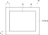
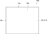
- FIG. 2 is a plan view of the gas barrier laminate of the present invention.
- the plan view is a view of the gas barrier laminate of the present invention as viewed from the direction orthogonal to the main surface of the support 12.
- the main surface is the largest surface of the sheet (film, plate).
- the area is the area of the main surface unless otherwise noted.
- the gas barrier laminate 10 shown in FIG. 1 is formed on the surface of a support 12, the first organic layer 14 formed on one surface (main surface) of the support 12, and the surface of the first organic layer 14 First inorganic layer 16, the second organic layer 14 formed on the surface of the first inorganic layer 16, and the second layer formed on the surface of the second organic layer 14 It has the inorganic layer 16 and the protective organic layer 18 which is an organic layer most separated from the support 12 and formed on the surface of the second inorganic layer 16.
- the gas barrier laminate of the present invention has an inorganic layer and an organic layer alternately, and in the organic layer and the inorganic layer laminated alternately, it is the organic layer that is most separated from the support.
- the organic layer most separated from the support 12 is the protective organic layer 18.
- the organic layer most distant from the support has a smaller area than the inorganic layer most distant from the support among the inorganic layers.
- the protective organic layer 18 which is the organic layer most separated from the support 12 is the formation surface (lower layer) of the second inorganic layer 16 which is most separated from the support 12, that is, the protective organic layer 18. The area is smaller than that of the inorganic layer 16 of the layer.
- the support 12 side is also referred to as "lower”
- the protective organic layer 18 side as "upper".
- the gas barrier laminate 10 of the illustrated example has, as a preferred embodiment, an organic-inorganic laminate type gas barrier having at least one combination of an inorganic layer 16 exhibiting gas barrier properties and an organic layer 14 serving as a base of the inorganic layer 16. It is a laminate.
- the gas barrier laminate 10 of the illustrated example has two sets of the combination of the inorganic layer 16 and the organic layer 14 to be the base and has the protective organic layer 18 thereon, the present invention There is no limitation.
- the gas barrier laminate of the present invention has one set of the combination of the inorganic layer 16 and the organic layer 14 to be the base, and has the protective organic layer 18 thereon.
- Support 12 ⁇ organic layer 14 ⁇ inorganic layer 16 A layer configuration of the protective organic layer 18 may be used.
- the gas barrier laminate of the present invention has three sets of the combination of the inorganic layer 16 and the organic layer 14 serving as a base, and the protective organic layer 18 thereon, the support 12-organic layer 14-inorganic layer 16
- the layer structure of the organic layer 14, the inorganic layer 16, the organic layer 14, the inorganic layer 16, and the protective organic layer 18 may be used.
- the gas barrier laminate of the present invention may have four or more sets of combinations of the inorganic layer 16 and the organic layer 14 to be a base, and may have the protective organic layer 18 thereon.
- the gas barrier laminate of the present invention may not have the organic layer 14 between the support 12 and the first inorganic layer 16 closest to the support 12. If it is an example of illustration, it is not necessary to have the 1st-layer organic layer 14 used as a foundation
- the gas barrier laminate of the present invention has the inorganic layer and the organic layer alternately on at least one surface side of the support, and among the inorganic layer and the organic layer formed alternately, the support If it is the organic layer that is the most separated, various layer configurations can be used.
- the support 12 may be a known resin-made sheet (film, plate) used as a support in various gas barrier films, various laminated functional films, and the like.
- the material of the support 12 is not limited, and various resin materials can be used as long as the organic layer 14, the inorganic layer 16 and the protective organic layer 18 can be formed.
- the material of the support 12 is, for example, polyethylene (PE), polyethylene naphthalate (PEN), polyamide (PA), polyethylene terephthalate (PET), polyvinyl chloride (PVC), polyvinyl alcohol (PVA), polyacrylonitrile (PAN) ), Polyimide (PI), transparent polyimide, polymethyl methacrylate resin (PMMA), polycarbonate (PC), polyacrylate, polymethacrylate, polypropylene (PP), polystyrene (PS), acrylonitrile butadiene styrene copolymer (ABS) And cyclic olefin copolymer (COC), cycloolefin polymer (COP), and triacetyl cellulose (TAC).
- PE polyethylene
- PEN polyethylene naphthalate
- PA polyamide
- the thickness of the support 12 can be set as appropriate depending on the application, material and the like.
- the thickness of the support 12 is from the viewpoint of sufficiently securing the mechanical strength of the gas barrier laminate 10 and from the viewpoint of securing the flexibility (flexibility) of the gas barrier laminate 10 and reducing the weight and thickness thereof. Therefore, the thickness is preferably 5 to 150 ⁇ m, and more preferably 10 to 100 ⁇ m.
- the support 12 may have a functional layer on its surface.
- the functional layer include a protective layer, a sealing layer, a light reflection layer, an antireflective layer, a light shielding layer, a planarization layer, a buffer layer, and a stress relaxation layer.
- the organic layer 14 and the protective organic layer 18 are layers made of, for example, an organic compound obtained by polymerizing (crosslinking or curing) a monomer, a dimer, an oligomer or the like.
- the organic layer 14 serving as the lower layer of the inorganic layer 16 is the organic layer 14 serving as a base for properly forming the inorganic layer 16.
- the first organic layer 14 formed on the surface of the support 12 embeds the irregularities on the surface of the support 12 and foreign matter attached to the surface, and the surface on which the first inorganic layer 16 is formed To make it possible to properly form the first inorganic layer 16.
- the second organic layer to be the lower layer of the second inorganic layer 16 also exhibits the same function. By having such an organic layer 14 to be a base, it is possible to properly form the inorganic layer 16 that mainly exhibits gas barrier properties.
- the protective organic layer 18 which is the organic layer most separated from the support 12 mainly protects the second inorganic layer 16 most separated from the support 12.
- Organic layer to That is, the protective organic layer 18 is an organic layer for protecting the lower inorganic layer 16.
- the gas barrier laminate 10 of the present invention can prevent damage to the inorganic layer 16 and maintain desired gas barrier properties.
- the protective organic layer 18 is the inorganic layer 16 most separated from the support 12 among the organic layers and the inorganic layers alternately formed, that is, the formation surface of itself. The area is smaller than the lower second inorganic layer 16. This point will be described in detail later.
- the organic layer 14 to be the base of the inorganic layer 16 and the protective organic layer 18 are basically the same. Therefore, the following description will be made with the organic layer 14 as a representative example, unless it is particularly necessary to distinguish.
- the organic layer 14 is formed, for example, by curing a composition for forming an organic layer containing an organic compound (monomer, dimer, trimer, oligomer, polymer and the like).
- the composition for forming an organic layer may contain only one type of organic compound, or may contain two or more types.
- the organic layer 14 contains, for example, a thermoplastic resin and an organic silicon compound.
- the thermoplastic resin is, for example, polyester, (meth) acrylic resin, methacrylic acid-maleic acid copolymer, polystyrene, transparent fluorine resin, polyimide, fluorinated polyimide, polyamide, polyamide imide, polyether imide, cellulose acylate, polyurethane And polyether ether ketone, polycarbonate, alicyclic polyolefin, polyarylate, polyether sulfone, polysulfone, fluorene ring modified polycarbonate, alicyclic modified polycarbonate, fluorene ring modified polyester, and an acrylic compound.
- organosilicon compounds include polysiloxanes.
- the organic layer 14 preferably includes a polymer of a radical curable compound and / or a cationic curable compound having an ether group from the viewpoint of excellent strength and the viewpoint of glass transition temperature.
- the organic layer 14 preferably contains a (meth) acrylic resin whose main component is a polymer such as a monomer or oligomer of (meth) acrylate from the viewpoint of lowering the refractive index of the organic layer 14. By lowering the refractive index, the organic layer 14 has high transparency and improved light transmittance.
- the organic layer 14 is more preferably a difunctional or more functional group such as dipropylene glycol di (meth) acrylate (DPGDA), trimethylolpropane tri (meth) acrylate (TMPTA), dipentaerythritol hexa (meth) acrylate (DPHA), etc.
- DPGDA dipropylene glycol di (meth) acrylate
- TMPTA trimethylolpropane tri (meth) acrylate
- DPHA dipentaerythritol hexa
- (meth) acrylates of (meth) acrylates polymers of (meth) acrylates such as dimers and oligomers, and more preferably polymers of (meth) acrylates of trifunctional or higher functionality such as monomers, dimers and oligomers
- (meth) acrylic resin containing as a main component In addition, a plurality of these (meth) acrylic resins may be used.
- the main component refers to the component
- composition for forming an organic layer preferably contains, in addition to the organic compound, an organic solvent, a surfactant, and a silane coupling agent.
- each organic layer 14 may be the same or different.
- the materials of the organic layer 14 and the protective organic layer 18 may be the same or different.
- the thickness of the organic layer 14 is preferably 0.5 to 5 ⁇ m, and more preferably 1 to 3 ⁇ m.
- the thickness of the organic layer 14 is preferably 0.5 to 5 ⁇ m, and more preferably 1 to 3 ⁇ m.
- each organic layer 14 may be the same or different.
- the organic layer 14 and the protective organic layer 18 may also be the same or different in thickness.
- the organic layer 14 can be formed by a known method depending on the material.
- the organic layer 14 can be formed by a coating method in which the composition for forming an organic layer described above is applied and the composition for forming an organic layer is dried.
- the organic compound in the composition for organic layer formation is polymerized (crosslinked) by further irradiating ultraviolet rays to the dried composition for organic layer formation, if necessary. .
- the organic layer 14 can be formed by so-called roll-to-roll.
- roll to roll is also referred to as "RtoR”.
- RtoR a sheet-like material is sent out from a roll formed by winding a long sheet-like material, film formation is performed while conveying the film-forming target sheet in the longitudinal direction, and the film-formed sheet material is rolled Manufacturing method.
- the inorganic layer 16 is a thin film containing an inorganic compound, and is provided on the surface of the organic layer 14.
- the inorganic layer 16 mainly exhibits gas barrier properties.
- the inorganic layer 16 is properly formed by being provided on the surface of the organic layer 14. For example, there are areas on the surface of the support 12 where it is difficult for an inorganic compound to form a film, such as irregularities and shadows of foreign matter.
- the organic layer 14 By providing the organic layer 14 on the support 12, the region where the inorganic compound is difficult to deposit is covered. Therefore, the inorganic layer 16 can be formed on the entire surface of the support 12 without a gap. In this respect, the same applies to the second and subsequent inorganic layers 16.
- the inorganic compound used for the well-known gas barrier layer which consists of an inorganic compound which expresses gas barrier property can be variously utilized.
- the material of the inorganic layer 16 include metal oxides such as aluminum oxide, magnesium oxide, tantalum oxide, zirconium oxide, titanium oxide and indium tin oxide (ITO); metal nitrides such as aluminum nitride; and metals such as aluminum carbide Carbides; Silicon oxides such as silicon oxide, silicon oxynitride, silicon oxycarbide, silicon oxynitride carbide, etc.
- Silicon nitrides such as silicon nitride and silicon carbonitride; Silicon carbides such as silicon carbide; Hydrides of these; And mixtures thereof, and inorganic compounds such as hydrogen-containing compounds thereof. Also, mixtures of two or more of these are available.
- silicon nitride, silicon oxide, silicon oxynitride, aluminum oxide, and a mixture of two or more of them are suitably used in that they have high transparency and can exhibit excellent gas barrier properties. Above all, silicon nitride is suitably used in that it can exhibit excellent gas barrier properties.
- the thickness of the inorganic layer 16 is preferably 10 to 150 nm, more preferably 12 to 100 nm, and still more preferably 15 to 75 nm. By setting the thickness of the inorganic layer 16 to 10 nm or more, it is preferable in that the inorganic layer 16 which can stably exhibit sufficient gas barrier performance can be formed. In addition, the inorganic layer 16 is generally brittle, and if it is too thick, there is a possibility of cracking, cracking, peeling and the like, but cracking occurs if the thickness of the inorganic layer 16 is 150 nm or less Can be prevented.
- each inorganic layer 16 may be the same or different.
- the inorganic layer 16 can be formed by a known method depending on the material. For example, plasma CVD such as CCP (Capacitively Coupled Plasma) -CVD (Chemical Vapor Deposition) and ICP (Inductively Coupled Plasma) -CVD, atomic layer deposition (ALD (Atomic Layer Deposition)), magnetron sputtering, reactive sputtering, etc. Sputtering and various vapor phase film forming methods such as vacuum evaporation are suitably mentioned.
- the inorganic layer 16 is also formed of RtoR.
- Such a gas barrier laminate 10 of the present invention is preferably suitably used as a substrate for forming an electronic device.
- FIG. 3 an example of the electronic device of this invention which uses the gas barrier laminate 10 of this invention is shown notionally.
- FIG. 3 shows an example in which the electronic device of the present invention is used for an organic electroluminescent lighting device (organic EL (Electro Luminescence) lighting device) as an example.
- the electronic device of the present invention is not limited to the organic EL lighting device 24.
- the electronic device of the present invention may be a solar cell (solar cell device) having a solar cell element instead of the organic EL lighting element 26.
- the electronic device of the present invention includes various known electronic devices such as organic EL devices other than organic EL lighting devices such as organic EL displays, electronic paper, and quantum dot devices using quantum dots. It is available. Above all, the electronic device of the present invention is suitably used for an organic EL lighting device and a solar cell.
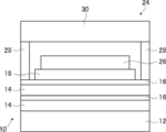
- the organic EL lighting device 24 shown in FIG. 3 forms an organic EL lighting element 26 on the surface of the protective organic layer 18 using the above-described gas barrier laminate 10 as a base material, and forms a rectangular frame so as to surround the protective organic layer 18
- the sealing layer 28 is provided, and the sealing base 30 is adhered to the sealing layer 28, whereby the organic EL lighting element 26 is sealed with the sealing base 30.
- the organic EL lighting device 24 may have various members of a known organic EL lighting device (organic EL device), such as a passivation film and a desiccant, as necessary. .
- the sealing base 30 side is also referred to as “upper”, and the support 12 side is also referred to as “lower”.
- the second inorganic layer 16 (the inorganic layer in which the protective organic layer 18 which is the organic layer most separated from the support 12 is the most separated from the support 12)
- the area is smaller than the lower inorganic layer 16) of the protective organic layer 18.
- the protective organic layer 18 is contained in the inorganic layer 16 in the lower layer. Ru.
- the organic EL lighting device 24 forms the organic EL lighting element 26 in the protective organic layer 18.
- the sealing layer 28 is a frame surrounding the protective organic layer 18 and the organic EL lighting element 26, and the sealing base 30 for sealing the organic EL lighting element 26 is placed on the sealing layer 28. Be glued. Therefore, in the illustrated organic EL lighting device 24, the protective organic layer 18 is not exposed to the outside including all the end faces.
- the gas barrier laminate 10 (organic EL lighting device 24) of the present invention suitably prevents the deterioration of the organic EL lighting element 26 due to moisture.
- the protective organic layer protects the lower inorganic layer (the uppermost inorganic layer in the inorganic layer) so that the gas barrier laminate exhibits and maintains predetermined gas barrier properties.
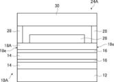
- the protective organic layer 18A is generally formed so as to cover the entire surface of the lower inorganic layer 16. Therefore, as shown in FIG. 6, the organic EL lighting device 24A using the conventional gas barrier laminate as a base material forms a frame-like sealing layer 28 on the protective organic layer 18A, and the sealing layer 28 is formed. By bonding the sealing base 30, the organic EL lighting element 26 is sealed by the sealing base 30. Therefore, in the conventional organic EL lighting device 24A, the end face 18e of the protective organic layer 18A is exposed to the outside.
- the protective organic layer 18A is for protecting the underlying inorganic layer 16.
- the inorganic layer 16 is, for example, a thin and hard film having a thickness of about 10 to 150 nm.
- the protective organic layer 18A needs to have a certain degree of hardness.
- the organic layer (layer made of an organic material) having a hardness that can sufficiently protect the thin and hard inorganic layer 16 does not have sufficient gas barrier properties. Therefore, in the conventional gas barrier laminate 10A in which the end face 18e of the protective organic layer 18A is exposed to the outside, moisture intrudes from the end face 18e of the protective organic layer 18A and reaches the organic EL lighting element 26.
- the protective organic layer 18A Without the protective organic layer 18A, the deterioration of the organic EL lighting element 26 due to moisture entering from the end face of the protective organic layer 18A can be prevented.
- the protective organic layer 18A when the protective organic layer 18A is not present, the inorganic layer 16 is exposed at the outermost surface, so when, for example, it is wound into a roll, it is cut into a predetermined shape, and in handling etc. The layer 16 is damaged, and the gas barrier laminate does not exhibit predetermined gas barrier properties.
- the area of the protective organic layer 18 is smaller than that of the lower inorganic layer 16.
- the protective organic layer 18 is included in the lower inorganic layer 16.
- various adhesives can be selected as the adhesive for forming the sealing layer 28 having sufficient gas barrier properties. Therefore, according to the gas barrier laminate 10 of the present invention, as shown in FIG. 3, the end face of the protective organic layer 18 is inside the sealing layer 28, and preferably, the protective organic layer 18 is preferably an inorganic layer 16 of the lower layer. , And can be enclosed by the sealing layer 28 and the sealing base 30.
- the organic EL lighting element 26 by moisture entering from the end face of the protective organic layer 18 Of the organic EL lighting device (electronic device) can be extended.
- the protective organic layer 18 is included in the lower inorganic layer 16 in a plan view.
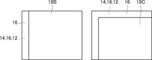
- the present invention is not limited thereto, and the protective organic layer 18 is smaller than the lower inorganic layer 16, and a part of the end face of the protective organic layer 18 is in the surface direction than the end face of the lower inorganic layer 16. It should be located inside. That is, in the gas barrier laminate 10 of the present invention, for example, as in a protective organic layer 18B shown on the left side of FIG. 4, only one end face may be positioned inside the end face of the lower inorganic layer 16 Alternatively, as in a protective organic layer 18C shown on the right side of FIG.
- the number of the end faces of the protective organic layer exposed to the outside be small. Therefore, in the gas barrier laminate of the present invention, as in the rectangular protective organic layer 18C shown on the right side of FIG. 4, the end faces (50% or more of all the end faces) of at least two sides of the protective organic layer
- the protective organic layer 18 is included in the lower inorganic layer 16 in the plan view as shown in FIGS. 1 and 2, that is, all the end faces of the protective organic layer 18. Is more preferably positioned inside the end face of the lower inorganic layer 16.
- a sealing layer so that the end face (50% or more of all the end faces) of at least two sides of the protective organic layer is inside in the surface direction. It is more preferable to provide the sealing layer 28 so as to surround the protective organic layer 18 in the plane direction as described above, and seal with the sealing base 30.
- the distance d between the end face of the protective organic layer 18 and the end face of the lower inorganic layer 16 there is no limit to Here, from the viewpoint of preventing the deterioration of the organic EL lighting element 26 caused by the moisture entering from the end face of the protective organic layer 18, the thickness (size in the surface direction) of the sealing layer 28 up to the protective organic layer 18 can be increased. In terms of point, it is preferable that the distance d between the end face of the protective organic layer 18 and the end face of the lower inorganic layer 16 be longer.
- the distance d between the end face of the protective organic layer 18 and the end face of the lower inorganic layer 16 is long, the area not covered by the protective organic layer 18 in the inorganic layer 16 increases, and the inorganic layer 16 is prone to damage.
- the distance d between the end face of the protective organic layer 18 and the end face of the lower inorganic layer 16 in at least a part of the end face preferably in an area of 50% or more in the plane direction Is preferably 1 to 10 mm, more preferably 1 to 8 mm, and still more preferably 1 to 7 mm.
- the sealing layer 28 is for bonding the sealing base 30 and sealing the organic EL lighting element 26 by the sealing base 30.
- the sealing substrate 30 is provided on the side of the organic EL lighting element 26 opposite to the protective organic layer 18. Specifically, in the organic EL lighting device 24, the organic EL lighting element 26 is sealed by the sealing base 30, the sealing layer 28, and the gas barrier laminate 10.
- the sealing layer 28 can be variously used as a sealing layer, a pressure-sensitive adhesive layer, and the like in a known organic EL device.
- a UV curable resin is preferable as the material of the sealing layer 28, and more specifically, a UV curable epoxy resin, a UV curable acrylate resin, and the like are exemplified.
- a commercially available adhesive can also be used suitably for the sealing layer 28, For example, XNR5516 by Nagase ChemteX Corp. etc. is illustrated.
- an adhesive sheet or an adhesive tape may be used as the sealing layer 28. Adhesive sheets and adhesive tapes, including commercial products, are widely available as what is known as OCA (Optical Clear Adhesive).
- the sealing layer 28 is provided in a frame shape surrounding the protective organic layer 18 (organic EL lighting element 26), and the region where the organic EL lighting element 26 is present is a space.
- the invention is not limited to this. That is, in the organic EL lighting device (electronic device), the space between the organic EL lighting element 26, the protective organic layer 18, the inorganic layer 16 under the protective organic layer 18, and the sealing base 30 is filled with the sealing layer It may be configured as described above. However, in terms of the optical characteristics of the organic EL lighting device 24 and the flexibility of the organic EL lighting device 24, the sealing layer 28 has a frame shape surrounding the protective organic layer 18, and the area where the organic EL lighting element 26 is present is a space. The configuration of FIG. 3 is more advantageous.
- the sealing layer 28 has a frame shape surrounding the protective organic layer 18, the distance d between the end face of the protective organic layer 18 and the end face of the inorganic layer 16 in the lower layer and the thickness of the sealing layer 28 ( Depending on the size in the surface direction, the sealing layer 28 may cover the end in the surface direction of the protective organic layer 18.
- the sealing layer 28 preferably has high gas barrier properties.
- the material of the sealing layer 28 has a water vapor transmission rate per 500 ⁇ m (water vapor transmission coefficient per 500 ⁇ m) of 1 ⁇ 10 ⁇ 1 to 1 ⁇ 10 ⁇ 3 g / (m 2 ⁇ day) Is more preferable, and 1 ⁇ 10 ⁇ 2 to 1 ⁇ 10 ⁇ 3 g / (m 2 ⁇ day) is more preferable.
- the sealing layer 28 preferably has a water vapor transmission rate of 1 ⁇ 10 ⁇ 1 to 1 ⁇ 10 ⁇ 3 g / (m 2 ⁇ day), and 1 ⁇ 10 ⁇ 2 to 1 ⁇ 10 ⁇ 3 g / (m 2 ⁇ day) is more preferred.
- the water vapor transmission rate of the sealing layer 28 as referred to herein means protection from the end face outside the sealing layer 28. It is the water vapor transmission rate of the sealing layer 28 in the thickness to the end face of the organic layer 18.
- the water vapor transmission rate of the sealing layer 28 means the thickness of the sealing layer 28 It is the water vapor transmission rate of the sealing layer 28 when it is regarded as from the outer end face of the sealing layer 28 to the end face of the protective organic layer 18.
- the sealing layer 28 has lower gas barrier properties than the sealing base 30 and the inorganic layer 16. Therefore, from the viewpoint of preventing the deterioration of the organic EL lighting element 26 due to moisture, it is advantageous that the height of the sealing layer 28 (the size in the vertical direction, that is, the direction orthogonal to the surface direction) be smaller. On the other hand, in order to apply the sealing layer 28 uniformly and seal the organic EL lighting element 26 precisely, it is preferable that the sealing layer 28 have a certain height. Specifically, the height of the sealing layer 28 is preferably 1 to 500 ⁇ m, more preferably 50 to 400 ⁇ m, and still more preferably 100 to 300 ⁇ m.
- the organic EL lighting element 26 is a known organic EL lighting element used for an organic EL lighting device (organic EL lighting device).
- the organic EL lighting element 26 includes an anode, a hole injection layer (hole injection layer), a hole transport layer (hole transport layer), a light emitting layer, a hole blocking layer (hole blocking layer), an electron transport layer,
- the sealing substrate 30 is also a known sealing substrate used for a known organic EL lighting device. Specifically, a sheet-like material made of yttria-stabilized zirconia (YSZ), glass (alkali-free glass, soda lime glass, etc.), etc. is exemplified.
- a gas barrier film formed by forming a gas barrier layer made of an inorganic compound on a resin film can also be suitably used. Examples of the gas barrier layer include a silicon nitride layer, a silicon oxide layer, a silicon oxynitride layer, and an aluminum oxide layer.
- the gas barrier layer side is directed to the organic EL lighting element 26, and sealing with the sealing base 30 is performed.
- the sealing substrate 30 includes one or more combinations of the same inorganic layer that exhibits gas barrier properties as the gas barrier laminate 10 shown in FIG. 1 and an organic layer that is a base of the inorganic layer.
- An organic-inorganic laminate type gas barrier film is also suitably usable.
- the organic-inorganic laminate type gas barrier film usually has a protective organic layer for protecting the inorganic layer by covering the uppermost inorganic layer as a layer most separated from the support.
- the gas barrier laminate of the present invention can also be used more suitably as illustrated in FIG. 5 to conceptually illustrate the gas barrier laminate 10.
- FIG. 5 to conceptually illustrate the gas barrier laminate 10.
- the sealing layer 28 is provided in a frame shape surrounding the protective organic layer 18, and the organic EL lighting device in which the area where the organic EL lighting element 26 exists is a space.
- the gas barrier film of the present invention is not the ordinary organic-inorganic laminated gas barrier film having a protective organic layer. It is preferable to use a gas barrier laminate or an organic-inorganic laminate type gas barrier film not having a protective organic layer.
- a support 12 such as a PET film is prepared, and the first organic layer 14 is formed on one surface of the support 12 by the coating method using the composition for forming an organic layer as described above.
- coating of the composition for organic layer formation can utilize well-known methods, such as the bar-coating method, the gravure coat method, and the die-coating method.
- the first inorganic layer 16 is formed on the surface of the first organic layer 14 by plasma CVD such as CCP-CVD.
- the protective organic layer 18 is formed similarly to the following.
- the second organic layer 14 and the second inorganic layer 16 are formed.
- the formation of the same organic layer 14 and the inorganic layer 16 may be repeated.
- a composition for forming the protective organic layer 18 (a composition for forming a protective organic layer) is applied to the entire surface of the inorganic layer 16 of the second layer (uppermost layer), and an organic layer is similarly formed.
- the formation of each of these layers preferably uses RtoR, as described above.
- the laminate prepared as necessary is cut into a predetermined shape, and then the periphery of the organic layer formed on the second inorganic layer 16 of the laminate is removed, and the inorganic material of the lower layer in the plan view is removed.
- the protective organic layer 18 included in the layer 16 is formed to obtain the gas barrier laminate 10 of the present invention.
- known methods can be used, but preferably etching is used. Although both dry etching and wet etching can be used as the etching, dry etching is preferably used in that the adhesion between the inorganic layer 16 and the sealing layer 28 can be improved.
- Dry etching is a method of etching a material by reactive gas, ions, radicals or the like.
- dry etching known methods such as plasma etching, ion etching, and focused ion beam etching can be used.
- Ion etching is a method of etching a solid surface with helium (He), argon (Ar), neon (Ne), an inert gas containing a combination thereof, or the like.
- Reactive ion etching RIE (Reactive Ion Etching)
- RIE Reactive Ion Etching
- the composition for forming an organic layer is applied to the entire surface of the inorganic layer 16, and the protective organic layer 18 is not formed by removing the periphery by etching.
- the composition for forming an organic layer may be applied so as to be included in the inorganic layer 16 in the figure to form the protective organic layer 18.
- an anode, a hole injection layer, a hole transport layer, a light emitting layer, a hole blocking layer, an electron transport layer, an electron injection layer, a cathode, etc. on the protective organic layer 18 To form the organic EL lighting element 26.
- an adhesive serving as the sealing layer 28 is applied in a frame shape to the exposed peripheral portion of the inorganic layer 16 under the protective organic layer 18.
- the sealing substrate 30 is laminated on the adhesive, and then the adhesive is cured by, for example, irradiation with ultraviolet light, and the inorganic layer 16 (gas barrier laminate 10) and the sealing substrate are sealed by the sealing layer 28
- the organic EL lighting device 24 is manufactured by bonding 30.
- Example 1 ⁇ Production of gas barrier laminate> As a support, a PET film (A4300, manufactured by Toyobo Co., Ltd.) having a thickness of 100 ⁇ m was prepared.
- the composition for organic layer formation for forming an organic layer was prepared.
- the solid content concentration of the composition for forming an organic layer was 15% by mass.
- the prepared composition for forming an organic layer was applied to the surface of the prepared support. The coating was performed using a die coater such that the film thickness of the organic layer was 1 ⁇ m. After application, it was dried in an oven at 80 ° C. for 3 minutes.
- the composition for forming an organic layer is cured by irradiating the ultraviolet rays of a high pressure mercury lamp (accumulated irradiation amount: about 600 mJ / cm 2 ) in a chamber in which the oxygen concentration is 0.1% by a nitrogen substitution method. A layer was formed.
- a silicon nitride film having a thickness of 40 nm was formed as an inorganic layer.
- the formation of the inorganic layer was performed using a CCP-CVD apparatus (manufactured by Samco).
- As raw material gases silane gas (flow rate 160 sccm: 0 ° C., standard condition at 1 atm, and so forth), ammonia gas (flow rate 370 sccm), hydrogen gas (flow rate 590 sccm), and nitrogen gas (flow rate 240 sccm) were used.
- the deposition pressure was 40 Pa.
- the power supply was a high frequency power supply with a frequency of 13.56 MHz, and the plasma excitation power was 2.5 kW.
- the organic layer between the support and the inorganic layer (the first inorganic layer) is also referred to as a base organic layer.
- An organic layer to be a protective organic layer having a thickness of 1.5 ⁇ m was formed on the inorganic layer using the prepared composition for forming a protective organic layer in the same manner as the organic layer formed above.
- a laminate having an organic layer, an inorganic layer, and an organic layer to be a protective organic layer formed on the surface of a support was produced.
- the laminate was cut into 50 ⁇ 50 mm. Thereafter, the entire peripheral portion (all four sides) of the organic layer to be a protective organic layer was removed by etching by 1 mm in a plane direction to form a protective organic layer.
- Two gas barrier laminates were prepared.
- the water vapor transmission rate of the manufactured gas barrier laminate was measured by the calcium corrosion method (the method described in JP-A-2005-283561). As a result, the water vapor transmission rate of the laminate was 1 ⁇ 10 ⁇ 6 g / (m 2 ⁇ day).
- a polyethylenedioxythiophene-polystyrene sulfonic acid (PEDOT-PSS) electrode (anode) was formed to a thickness of 80 nm on the surface of one protective organic layer of the produced gas barrier laminate.
- a molybdenum oxide (MoO 3 ) layer of 2 nm is formed as a hole injection layer on the surface of the formed anode as a hole injection layer, and a hole transport layer ( ⁇ -NPD: Bis [) is sequentially formed on the surface of the molybdenum oxide layer.
- LiF lithium fluoride
- aluminum 1.5 nm
- silver 15 nm
- An organic EL lighting element was formed.
- An adhesive (XNR 5516, manufactured by Nagase ChemteX Corp.) was applied in a frame shape on the periphery of the upper surface (the surface on the protective organic layer side) of the gas barrier laminate in which the organic EL lighting element was formed.
- the adhesive cures, the water vapor transmission rate per 500 ⁇ m is 1 ⁇ 10 ⁇ 1 g / (m 2 ⁇ day).
- the other gas barrier laminate was used as a sealing base material, and the end portion was aligned with the upper surface side facing the organic EL lighting element side and laminated.
- the adhesive was cured to form a sealing layer by irradiating ultraviolet rays of a high pressure mercury lamp (total irradiation amount: approximately 6 J / cm 2 ).
- the organic EL lighting element is sealed by bonding the gas barrier laminate in which the organic EL lighting element is formed and the sealing base (the same gas barrier laminate) with a sealing layer, as shown in FIG.
- An EL lighting device was manufactured.
- the height (size in the vertical direction) of the formed sealing layer was 500 ⁇ m, and the thickness (size in the surface direction) of the sealing layer was 5 mm.
- a 4 mm sealing layer covers the end of the protective organic layer.
- Example 2 and Example 3 In the production of one gas barrier laminate, etching of the peripheral portion of the organic layer to be a protective organic layer is performed on two adjacent sides (see Example 2, right side in FIG. 4) and one side (Examples 3, 4) A gas barrier laminate was produced in the same manner as in Example 1 except that the left side was referred to). An organic EL lighting device was produced in the same manner as in Example 1 except that the organic EL lighting element was formed on the gas barrier laminate.
- the gas barrier laminate used as a sealing base material is the same as Example 1. About this point, it is the same as that of all the examples which changed the composition of the gas barrier layered product which forms an organic EL lighting element. Therefore, in Example 2, the end faces of the two sides are exposed to the outside in the protective organic layer of the gas barrier laminate in which the organic EL lighting element is formed, and in Example 3, the end faces of the three sides are exposed to the outside It has become.
- Example 4 In the preparation of one gas barrier laminate, the etching width of the peripheral part of the organic layer to be the protective organic layer is changed to 0.5 mm, 7 mm, 8 mm, 10 mm and 11 mm, and the end face of the protective organic layer and the lower layer Distance to the end face of the inorganic layer (distance d in FIGS. 1 and 2) is 0.5 mm (Example 4), 7 mm (Example 5), 8 mm (Example 6), 10 mm (Example 7), And, a gas barrier laminate was produced in the same manner as in Example 1 except that it was changed to 11 mm (Example 8). An organic EL lighting device was produced in the same manner as in Example 1 except that the organic EL lighting element was formed on the gas barrier laminate.
- Example 9 A gas barrier laminate was produced in the same manner as in Example 1 except that in the production of one gas barrier laminate, the organic layer (underlying organic layer) between the support and the inorganic layer was not formed. That is, this gas barrier laminate has a layer configuration of a support, an inorganic layer, and a protective organic layer.
- An organic EL lighting device was produced in the same manner as in Example 1 except that the organic EL lighting element was formed on the gas barrier laminate.
- Example 10 In the preparation of one gas barrier laminate, after forming the second organic layer, the second inorganic layer is formed on the surface of the second organic layer in the same manner as the first inorganic layer, The same as Example 1 except that the third organic layer was formed on the surface of the second inorganic layer in the same manner as the second organic layer, and the third organic layer was a protective organic layer.
- a gas barrier laminate was produced. That is, this gas barrier laminate has a layer structure of a support, an organic layer, an inorganic layer, an organic layer, an inorganic layer, and a protective organic layer.
- An organic EL lighting device was produced in the same manner as in Example 1 except that an organic EL lighting element was formed on the gas barrier laminate, and the height of the sealing layer was set to 300 ⁇ m.
- the sealing layer has a height of 0.5 ⁇ m (Example 11), 600 ⁇ m (Example 12), 50 ⁇ m (Example 13), 400 ⁇ m (Example 14), 100 ⁇ m (Example 15), and 300 ⁇ m (Examples)
- a gas barrier laminate was produced in the same manner as in Example 1 except that the example was changed to 16).
- An organic EL lighting device was produced in the same manner as in Example 1 except that this gas barrier laminate was used.
- Comparative Example 1 In the preparation of one gas barrier laminate, a gas barrier laminate was prepared in the same manner as in Example 1 except that the periphery of the organic layer to be the protective organic layer was not etched. An organic EL lighting device was produced in the same manner as in Example 1 except that the organic EL lighting element was formed on the gas barrier laminate. Therefore, all the edge parts of four sides of the protective organic layer of the gas barrier laminate in which the organic EL lighting element is formed are exposed to the outside.
- Evaluation of the produced organic electroluminescent illuminating device was performed as follows.
- the prepared organic EL lighting device is left in an environment of temperature 60 ° C. and relative humidity 90% RH for 100 hours, and the total area [%] of dark spots with respect to the total light emitting area (area of organic EL lighting element) is shown in the table below. Shown in.
- the gas barrier laminate of the present invention in which the protective organic layer is smaller than the lower inorganic layer and the end face of at least one side is inward in the plane direction from the sealing layer and According to the organic EL lighting device, it has higher high temperature and high humidity durability than that of Comparative Example 1 in which all the end faces of the four sides of the protective organic layer are exposed to the outside, that is, the gas barrier of the gas barrier laminate Sex is excellent.
- Example 1 and Examples 5 to 7 by setting the distance between the end face of the protective organic layer and the end face of the lower inorganic layer in the range of 1 to 10 mm, higher temperature and high humidity durability, ie, better The gas barrier properties of the gas barrier laminate can be obtained.
- Example 8 since the distance between the end face of the protective organic layer and the end face of the lower inorganic layer is 11 mm, which is slightly longer than in Example 7, the inorganic layer is slightly removed during handling before sealing. It is considered that there were more dark spots than in Example 7 due to a lot of damage.
- Example 9 From the comparison between Example 9 and Example 1, by providing the organic layer (underlying organic layer) between the support and the first inorganic layer, good high temperature and high humidity durability, that is, the gas barrier of the gas barrier laminate is obtained. Sex is obtained. Furthermore, as shown in Examples 13 to 16, by setting the height of the sealing layer in the range of 50 to 400 ⁇ m, in particular in the range of 100 to 300 ⁇ m, the high temperature high humidity durability, ie, more excellent. The gas barrier properties of the gas barrier laminate can be obtained. In addition, as shown in Example 10, the height of the sealing layer is in the range of 100 to 300 ⁇ m, and the combination of the organic layer serving as the base and the inorganic layer is two sets (two inorganic layers). Thus, the very high temperature and high humidity durability, that is, the gas barrier properties of the gas barrier laminate can be obtained. From the above results, the effects of the present invention are clear.
Landscapes
- Electroluminescent Light Sources (AREA)
- Laminated Bodies (AREA)
- Photovoltaic Devices (AREA)
Abstract
L'invention concerne : un stratifié de barrière aux gaz qui est capable d'empêcher la détérioration d'un dispositif électronique causée par l'humidité ; et un dispositif électronique qui utilise ce stratifié de barrière aux gaz. Un stratifié de barrière aux gaz selon la présente invention comprend : un corps de support ; et une ou plusieurs couches inorganiques et une ou plusieurs couches organiques, qui sont stratifiées alternativement sur le corps de support. Parmi les couches inorganiques et les couches organiques stratifiées alternativement, une couche organique est positionnée le plus loin du corps de support, et cette couche organique positionnée le plus loin du corps de support a une aire inférieure à celle d'une couche inorganique qui est positionnée le plus loin du corps de support parmi les couches inorganiques.
Applications Claiming Priority (2)
| Application Number | Priority Date | Filing Date | Title |
|---|---|---|---|
| JP2017-146343 | 2017-07-28 | ||
| JP2017146343A JP2020157476A (ja) | 2017-07-28 | 2017-07-28 | ガスバリア積層体および電子デバイス |
Publications (1)
| Publication Number | Publication Date |
|---|---|
| WO2019021616A1 true WO2019021616A1 (fr) | 2019-01-31 |
Family
ID=65040590
Family Applications (1)
| Application Number | Title | Priority Date | Filing Date |
|---|---|---|---|
| PCT/JP2018/020701 Ceased WO2019021616A1 (fr) | 2017-07-28 | 2018-05-30 | Stratifié de barrière aux gaz et dispositif électronique |
Country Status (2)
| Country | Link |
|---|---|
| JP (1) | JP2020157476A (fr) |
| WO (1) | WO2019021616A1 (fr) |
Cited By (2)
| Publication number | Priority date | Publication date | Assignee | Title |
|---|---|---|---|---|
| WO2020208854A1 (fr) * | 2019-04-11 | 2020-10-15 | パナソニックIpマネジメント株式会社 | Module de cellules solaires |
| US20230102880A1 (en) * | 2021-07-28 | 2023-03-30 | Tomoya Hirano | Photoelectric conversion device, electronic device, and power supply module |
Citations (3)
| Publication number | Priority date | Publication date | Assignee | Title |
|---|---|---|---|---|
| JP2012051172A (ja) * | 2010-08-31 | 2012-03-15 | Fujifilm Corp | 機能性フィルムおよび機能性フィルムの製造方法 |
| JP2013188942A (ja) * | 2012-03-14 | 2013-09-26 | Konica Minolta Inc | 水蒸気バリアーフィルムの製造方法、水蒸気バリアーフィルム及び電子機器 |
| JP2016159510A (ja) * | 2015-03-02 | 2016-09-05 | 凸版印刷株式会社 | ガスバリアフィルム及びその製造方法 |
-
2017
- 2017-07-28 JP JP2017146343A patent/JP2020157476A/ja active Pending
-
2018
- 2018-05-30 WO PCT/JP2018/020701 patent/WO2019021616A1/fr not_active Ceased
Patent Citations (3)
| Publication number | Priority date | Publication date | Assignee | Title |
|---|---|---|---|---|
| JP2012051172A (ja) * | 2010-08-31 | 2012-03-15 | Fujifilm Corp | 機能性フィルムおよび機能性フィルムの製造方法 |
| JP2013188942A (ja) * | 2012-03-14 | 2013-09-26 | Konica Minolta Inc | 水蒸気バリアーフィルムの製造方法、水蒸気バリアーフィルム及び電子機器 |
| JP2016159510A (ja) * | 2015-03-02 | 2016-09-05 | 凸版印刷株式会社 | ガスバリアフィルム及びその製造方法 |
Cited By (6)
| Publication number | Priority date | Publication date | Assignee | Title |
|---|---|---|---|---|
| WO2020208854A1 (fr) * | 2019-04-11 | 2020-10-15 | パナソニックIpマネジメント株式会社 | Module de cellules solaires |
| JPWO2020208854A1 (fr) * | 2019-04-11 | 2020-10-15 | ||
| CN113544872A (zh) * | 2019-04-11 | 2021-10-22 | 松下知识产权经营株式会社 | 太阳能电池模块 |
| JP7390668B2 (ja) | 2019-04-11 | 2023-12-04 | パナソニックIpマネジメント株式会社 | 太陽電池モジュール |
| CN113544872B (zh) * | 2019-04-11 | 2025-06-17 | 松下知识产权经营株式会社 | 太阳能电池模块 |
| US20230102880A1 (en) * | 2021-07-28 | 2023-03-30 | Tomoya Hirano | Photoelectric conversion device, electronic device, and power supply module |
Also Published As
| Publication number | Publication date |
|---|---|
| JP2020157476A (ja) | 2020-10-01 |
Similar Documents
| Publication | Publication Date | Title |
|---|---|---|
| TWI637542B (zh) | 有機el積層體 | |
| TWI587554B (zh) | 機能性膜 | |
| JP5090197B2 (ja) | 積層体の製造方法、バリア性フィルム基板、デバイスおよび光学部材 | |
| CN103764386A (zh) | 屏障层合物和气体屏障膜 | |
| US20170100926A1 (en) | Method of manufacturing electronic device and composite film | |
| JP6377541B2 (ja) | フレキシブルデバイスの製造方法、および、フレキシブルデバイス積層体 | |
| JP6321169B2 (ja) | 封止積層体および有機電子装置 | |
| JP6026331B2 (ja) | 有機el積層体 | |
| WO2015141252A1 (fr) | Dispositif électroluminescent organique | |
| JP2007216435A (ja) | ガスバリアフィルム基板、電極付きガスバリアフィルム基板、及びそれらを用いた表示素子 | |
| US11203180B2 (en) | Gas barrier film and method for producing gas barrier film | |
| KR101917552B1 (ko) | 유기 일렉트로 루미네선스 장치 | |
| WO2019021616A1 (fr) | Stratifié de barrière aux gaz et dispositif électronique | |
| JP2017041412A (ja) | 電子装置 | |
| US20200216950A1 (en) | Structured film and articles thereof | |
| JP2020129429A (ja) | 有機エレクトロルミネッセンス発光装置 | |
| WO2016009778A1 (fr) | Film composite | |
| JP6196944B2 (ja) | 封止部材および電子デバイスの製造方法 | |
| JP6343250B2 (ja) | ガスバリアフィルム、有機電子装置、有機電界発光装置用基板、有機電界発光装置 | |
| KR102345795B1 (ko) | 배리어 필름 구조체 및 이를 구비하는 유기전자소자 | |
| JP2008173837A (ja) | ガスバリア性積層基板及びその製造方法 |
Legal Events
| Date | Code | Title | Description |
|---|---|---|---|
| 121 | Ep: the epo has been informed by wipo that ep was designated in this application |
Ref document number: 18838356 Country of ref document: EP Kind code of ref document: A1 |
|
| NENP | Non-entry into the national phase |
Ref country code: DE |
|
| 122 | Ep: pct application non-entry in european phase |
Ref document number: 18838356 Country of ref document: EP Kind code of ref document: A1 |
|
| NENP | Non-entry into the national phase |
Ref country code: JP |