WO2019021764A1 - Actionneur et procédé de fabrication d'actionneur - Google Patents
Actionneur et procédé de fabrication d'actionneur Download PDFInfo
- Publication number
- WO2019021764A1 WO2019021764A1 PCT/JP2018/025218 JP2018025218W WO2019021764A1 WO 2019021764 A1 WO2019021764 A1 WO 2019021764A1 JP 2018025218 W JP2018025218 W JP 2018025218W WO 2019021764 A1 WO2019021764 A1 WO 2019021764A1
- Authority
- WO
- WIPO (PCT)
- Prior art keywords
- coil
- substrate
- base
- magnetic sensor
- actuator
- Prior art date
- Legal status (The legal status is an assumption and is not a legal conclusion. Google has not performed a legal analysis and makes no representation as to the accuracy of the status listed.)
- Ceased
Links
Images


Classifications
-
- H—ELECTRICITY
- H02—GENERATION; CONVERSION OR DISTRIBUTION OF ELECTRIC POWER
- H02K—DYNAMO-ELECTRIC MACHINES
- H02K3/00—Details of windings
- H02K3/04—Windings characterised by the conductor shape, form or construction, e.g. with bar conductors
- H02K3/26—Windings characterised by the conductor shape, form or construction, e.g. with bar conductors consisting of printed conductors
-
- H—ELECTRICITY
- H02—GENERATION; CONVERSION OR DISTRIBUTION OF ELECTRIC POWER
- H02K—DYNAMO-ELECTRIC MACHINES
- H02K11/00—Structural association of dynamo-electric machines with electric components or with devices for shielding, monitoring or protection
- H02K11/20—Structural association of dynamo-electric machines with electric components or with devices for shielding, monitoring or protection for measuring, monitoring, testing, protecting or switching
- H02K11/21—Devices for sensing speed or position, or actuated thereby
- H02K11/215—Magnetic effect devices, e.g. Hall-effect or magneto-resistive elements
-
- G—PHYSICS
- G03—PHOTOGRAPHY; CINEMATOGRAPHY; ANALOGOUS TECHNIQUES USING WAVES OTHER THAN OPTICAL WAVES; ELECTROGRAPHY; HOLOGRAPHY
- G03B—APPARATUS OR ARRANGEMENTS FOR TAKING PHOTOGRAPHS OR FOR PROJECTING OR VIEWING THEM; APPARATUS OR ARRANGEMENTS EMPLOYING ANALOGOUS TECHNIQUES USING WAVES OTHER THAN OPTICAL WAVES; ACCESSORIES THEREFOR
- G03B5/00—Adjustment of optical system relative to image or object surface other than for focusing
-
- H—ELECTRICITY
- H02—GENERATION; CONVERSION OR DISTRIBUTION OF ELECTRIC POWER
- H02K—DYNAMO-ELECTRIC MACHINES
- H02K1/00—Details of the magnetic circuit
- H02K1/06—Details of the magnetic circuit characterised by the shape, form or construction
- H02K1/12—Stationary parts of the magnetic circuit
- H02K1/18—Means for mounting or fastening magnetic stationary parts on to, or to, the stator structures
-
- H—ELECTRICITY
- H02—GENERATION; CONVERSION OR DISTRIBUTION OF ELECTRIC POWER
- H02K—DYNAMO-ELECTRIC MACHINES
- H02K11/00—Structural association of dynamo-electric machines with electric components or with devices for shielding, monitoring or protection
- H02K11/30—Structural association with control circuits or drive circuits
- H02K11/33—Drive circuits, e.g. power electronics
-
- H—ELECTRICITY
- H02—GENERATION; CONVERSION OR DISTRIBUTION OF ELECTRIC POWER
- H02K—DYNAMO-ELECTRIC MACHINES
- H02K15/00—Processes or apparatus specially adapted for manufacturing, assembling, maintaining or repairing of dynamo-electric machines
- H02K15/04—Processes or apparatus specially adapted for manufacturing, assembling, maintaining or repairing of dynamo-electric machines of windings prior to their mounting into the machines
-
- H—ELECTRICITY
- H02—GENERATION; CONVERSION OR DISTRIBUTION OF ELECTRIC POWER
- H02K—DYNAMO-ELECTRIC MACHINES
- H02K41/00—Propulsion systems in which a rigid body is moved along a path due to dynamo-electric interaction between the body and a magnetic field travelling along the path
- H02K41/02—Linear motors; Sectional motors
- H02K41/03—Synchronous motors; Motors moving step by step; Reluctance motors
- H02K41/031—Synchronous motors; Motors moving step by step; Reluctance motors of the permanent magnet type
- H02K41/033—Synchronous motors; Motors moving step by step; Reluctance motors of the permanent magnet type with armature and magnets on one member, the other member being a flux distributor
-
- H—ELECTRICITY
- H02—GENERATION; CONVERSION OR DISTRIBUTION OF ELECTRIC POWER
- H02K—DYNAMO-ELECTRIC MACHINES
- H02K41/00—Propulsion systems in which a rigid body is moved along a path due to dynamo-electric interaction between the body and a magnetic field travelling along the path
- H02K41/02—Linear motors; Sectional motors
- H02K41/035—DC motors; Unipolar motors
- H02K41/0352—Unipolar motors
- H02K41/0354—Lorentz force motors, e.g. voice coil motors
- H02K41/0356—Lorentz force motors, e.g. voice coil motors moving along a straight path
Definitions
- the present invention relates to an actuator, and more particularly to an actuator that moves one by the interaction of a coil and a magnet.
- Patent Document 1 discloses an actuator including a coil substrate on which a coil is formed, a base substrate to which the coil substrate is bonded, and a magnetic sensor mounted on the base substrate.
- the actuator moves a movable body provided with a magnet by a magnetic field generated by a coil.
- the current flowing through the coil is controlled by, for example, a driver IC connected to the magnetic sensor based on information (signal from the magnetic sensor) obtained from the magnetic sensor. Therefore, when the mounting position of the coil with respect to the magnetic sensor is deviated, the magnetic field detected by the magnetic sensor, the magnetic field generated by the coil, and the like may change from the defined state, and the characteristics of the actuator may vary.
- An object of the present invention is to provide an actuator including a coil substrate, a base substrate, and a magnetic sensor, in which an individual difference in actuator characteristics is suppressed by suppressing a shift in a positional relationship of the coil with respect to the magnetic sensor. .
- the actuator of the present invention is A coil substrate provided with a magnetic sensor and having a coil; A base substrate on which a coil drive circuit is formed; Equipped with The coil substrate is connected to the base substrate through a conductive bonding material.
- the coil substrate on which the magnetic sensor is provided in advance is mounted on the base substrate via the conductive bonding material, when the coil substrate is mounted on the base substrate, the positional relationship between the magnetic sensor and the coil deviates Is hard to occur. Therefore, compared with the case where the magnetic sensor and the coil substrate are mounted on the base substrate, the position of the coil with respect to the magnetic sensor can be hardly shifted from the predetermined position. Therefore, with this configuration, it is possible to suppress the variation in the characteristics of the actuator caused by the displacement of the position of the coil with respect to the magnetic sensor.
- a shield conductor provided on the base substrate may be provided, and the shield conductor may be disposed between the other conductive pattern formed on the base substrate and the magnetic sensor. preferable.
- the shield conductor since the shield conductor is located between the other conductor pattern formed on the base substrate and the magnetic sensor, noise generated from the other conductor pattern is shielded by the shield conductor. Therefore, with this configuration, the influence of noise generated from the base substrate on the magnetic sensor can be suppressed.
- the coil substrate includes a base formed by laminating a plurality of insulating base layers, and the coil is formed of the plurality of insulating base layers. It may be formed including a plurality of coil conductors formed in two or more insulating base layers.
- a coil is formed by including a plurality of coil conductors respectively formed in two or more insulating base layers, a plurality of insulating base layers (specifically, a plurality of coils) in order to suppress a change in characteristics of the coil. It is necessary to laminate conductors) with high positional accuracy.
- the yield rate of the actuator can be increased as compared with the case where the coil substrate and the base substrate are integrally formed. .
- the base material has a mounting surface to be mounted on the base substrate, and the magnet is disposed on the opposite side of the coil substrate from the base substrate, Preferably, the magnetic sensor is disposed closer to the magnet than the mounting surface. According to this configuration, since the distance between the magnetic sensor and the magnet is short as compared with the case where the magnetic sensor is mounted on the mounting surface, the magnetic field detection accuracy of the magnetic sensor with respect to the magnet can be improved.
- the coil drive circuit is connected to the magnetic sensor, and has a driver IC that controls the current flowing to the coil based on a signal from the magnetic sensor. It may be done.
- the wiring length between the driver IC and the capacitor or the wiring length between the capacitor and the ground can be shortened as compared with the case where the capacitor is mounted on the coil substrate. Therefore, the inductance and conductor resistance in the wiring between the driver IC and the capacitor, or the inductance and conductor resistance in the wiring between the capacitor and the ground can be reduced, and the effect of suppressing the voltage fluctuation of the driver IC by the capacitor is enhanced.
- the base substrate may have a flexible portion having flexibility and a connection portion for external connection connected to the flexible portion.
- the connection portion can be easily connected to another substrate or the like by utilizing the flexibility of the flexible portion (in a state where the flexible portion is bent).
- an external force is applied to the connection portion (for example, when another substrate connected to the connection portion moves)
- stress is hardly transmitted to the coil and the magnetic sensor. Therefore, it is possible to suppress the change in the characteristics of the actuator caused by the transfer of stress to the coil and the magnetic sensor.
- the method of manufacturing an actuator according to the present invention A coil substrate provided with a magnetic sensor and having a coil and a substrate; A base substrate on which a coil drive circuit is formed; A magnet that receives a magnetic field generated by the coil; A method of manufacturing an actuator comprising A coil substrate forming step of providing the magnetic sensor on the substrate; A substrate bonding step of connecting the coil substrate to the base substrate through a conductive bonding material after the coil substrate forming step; It is characterized by having.
- the coil substrate forming step may include the step of mounting the magnetic sensor on the base material.
- the base is formed by laminating a plurality of insulating base layers, and the coil substrate forming step includes the plurality of insulating base layers on which the magnetic sensor is mounted. You may include the process of laminating
- an actuator provided with a coil substrate, a base substrate, and a magnetic sensor, by suppressing the deviation of the positional relationship of the coil with respect to the magnetic sensor, it is possible to realize an actuator in which variations in characteristics among individuals are suppressed.
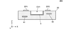
- FIG. 1 is a cross-sectional view of an actuator 301 according to the first embodiment.
- FIG. 2A is a cross-sectional view of the coil substrate 101 according to the first embodiment, and FIG. 2B is a plan view of the coil substrate 101.
- FIG. 3 is a cross-sectional view of the base substrate 201 according to the first embodiment.
- FIG. 4A is a cross-sectional view of an actuator 302 according to the second embodiment, and FIG. 4B is a cross-sectional view of a base substrate 202 according to the second embodiment.
- FIG. 5A is a cross-sectional view of an actuator 303 according to the third embodiment, and FIG. 5B is a cross-sectional view of a coil substrate 103 according to the third embodiment.
- FIG. 6 is a cross-sectional view of an actuator 304 according to the fourth embodiment.
- FIG. 1 is a cross-sectional view of an actuator 301 according to the first embodiment.
- FIG. 2A is a cross-sectional view of the coil substrate 101 according to the first embodiment
- FIG. 2B is a plan view of the coil substrate 101.
- FIG. 3 is a cross-sectional view of the base substrate 201 according to the first embodiment. The thickness of each part is exaggerated and shown in FIG. 1, FIG. 2 (A), and FIG. The same applies to the cross-sectional views shown later.
- the "actuator" of the present invention is provided with a coil substrate having a coil and a base substrate as described later in detail, and moves a movable body provided with a magnet by a magnetic field generated by the coil.
- the actuator 301 includes a coil substrate 101, a base substrate 201, a magnet 4 and the like.
- the coil substrate 101 has a base 10, a coil L1, connection electrodes P1, P2, P11, P12, a magnetic sensor 1 and the like as shown in FIG. 2 (A) and FIG. 2 (B).
- the base 10 is a substantially rectangular parallelepiped whose longitudinal direction coincides with the X-axis direction, and has a first main surface VS1 and a second main surface VS2 facing each other.
- the base 10 is a laminate formed by laminating a plurality of insulating base layers made of thermoplastic resin.
- the substrate 10 is, for example, a rectangular solid mainly composed of a liquid crystal polymer (LCP) or a polyetheretherketone (PEEK).
- the first main surface VS1 of the base 10 corresponds to the “mounting surface” in the present invention.
- the coil L1 is an approximately four-turn coil formed inside the base 10 and having a winding axis AX along the stacking direction (Z-axis direction) of the plurality of insulating base layers.
- the coil L1 is configured of coil conductors 31 and 32 and an interlayer connection conductor (not shown).
- the coil conductors 31 and 32 are rectangular spiral conductor patterns of about 2 turns formed on different insulating base layers.
- the first end of the coil conductor 31 is connected to the first end of the coil conductor 32 via an interlayer connection conductor (not shown).
- the coil conductors 31 and 32 are conductor patterns, such as Cu foil, for example.
- connection electrodes P1, P2, P11, and P12 are rectangular conductor patterns formed on the first main surface VS1 of the base material 10.
- the connection electrode P1 is connected to the first end of the coil L1 (the second end of the coil conductor 31), and the connection electrode P2 is connected to the second end of the coil L1 (the second end of the coil conductor 32) There is.
- the connection electrodes P1, P2, P11 and P12 are conductor patterns of, for example, Cu foil.
- the magnetic sensor 1 is an element that senses a magnetic field generated when a current flows in the coil L1 or a magnetic field from the outside, and detects the amount of movement of the magnet 4.
- the magnetic sensor 1 is, for example, a Hall element utilizing a Hall effect.
- the magnetic sensor 1 is provided on the first main surface VS1 of the substrate 10. Specifically, the magnetic sensor 1 has terminals P21 and P22 on the mounting surface (the upper surface of the magnetic sensor 1 in FIG. 2A), and these terminals P21 and P22 are connected via the conductive bonding material 3 The connection electrodes P11 and P12 are respectively connected. As shown in FIG. 2A, the magnetic sensor 1 is disposed at a position overlapping the winding axis AX of the coil L1.
- the conductive bonding material 3 is, for example, a solder.
- the base substrate 201 has a base 20, a cavity CV1 formed on the base 20, a shield conductor 5, connection electrodes EP1 and EP2 formed on the base 20, conductor patterns 41 and 42, and the like. On the base substrate 201, a coil drive circuit for driving the coil L1 is formed.
- the base material 20 is a substantially rectangular parallelepiped whose longitudinal direction coincides with the X-axis direction.
- the base 20 is a laminate formed by laminating a plurality of insulating base layers made of thermoplastic resin.
- the substrate 20 is, for example, a substantially rectangular parallelepiped mainly composed of a liquid crystal polymer (LCP) or a polyetheretherketone (PEEK).
- the cavity CV1 is an opening formed inward (in the ⁇ Z direction) from the surface of the substrate 20 (the upper surface of the substrate 20 in FIG. 3).
- the planar shape of the cavity CV1 is a shape that matches the planar shape of the magnetic sensor 1.
- the magnetic sensor 1 is disposed in the cavity CV1.
- the cavity CV1 is formed, for example, by etching the surface side of the substrate 20 with a laser after forming the substrate 20.
- the shield conductor 5 is a box-shaped conductive member without a top surface, and is fitted in the cavity CV1.
- the shield conductor 5 is obtained, for example, by forming a flat plate made of Cu by plastic deformation (forging).
- connection electrodes EP1 and EP2 are rectangular conductor patterns formed on the surface of the substrate 20 (the upper surface of the substrate 20 in FIG. 3).
- the conductor patterns 41 and 42 are conductor patterns formed inside the base material 20.
- the connection electrodes EP1 and EP2 and the conductor patterns 41 and 42 are, for example, conductor patterns such as Cu foil.
- the coil substrate 101 is connected to the base substrate 201 via the conductive bonding material 3.
- the connection electrodes P1 and P2 of the coil substrate 101 are connected to the connection electrodes EP1 and EP2 of the base substrate 201 via the conductive bonding material 3.
- the coil substrate 101 and the base substrate 201 are connected in a state where the magnetic sensor 1 provided on the coil substrate 101 (base material 10) is disposed in the cavity CV1. Ru. Further, as shown in FIG. 1, the shield conductor 5 is disposed between the magnetic sensor 1 and another conductor pattern (conductor patterns 41 and 42) formed on the base substrate 201.
- the magnet 4 is attached to a movable body (not shown).
- the magnet 4 is disposed on the opposite side (+ Z direction) to the base substrate 201 with the coil substrate 101 interposed therebetween.
- the magnet 4 is, for example, a permanent magnet.
- the actuator 301 is used, for example, as follows.
- the magnet 4 is displaced in the planar direction (for example, the X-axis direction) by the magnetic field radiated from the coil L1 (see the white arrow in FIG. 1).
- the magnetic sensor 1 senses a change in magnetic field when the magnet 4 is displaced.
- the actuator 301 according to the present embodiment has the following effects.
- the shield conductor 5 is disposed between the magnetic sensor 1 and another conductor pattern (conductor patterns 41 and 42) formed on the base substrate 201. According to this configuration, noise generated from other conductor patterns is shielded by the shield conductor 5. Therefore, the influence of the noise generated from the base substrate 201 on the magnetic sensor 1 can be suppressed.
- the magnetic sensor 1 is disposed at a position overlapping the winding axis AX of the coil L1.
- the magnetic sensor 1 since the magnetic sensor 1 is disposed on the winding axis AX of the coil L1 less affected by the magnetic field generated from the coil L1, the influence of the magnetic field generated from the coil L1 can be reduced. Therefore, the magnetic field detection accuracy of the magnetic sensor 1 can be enhanced.
- the base material 10 of the coil substrate 101 and the base material 20 of the base substrate 201 are made of the same main component material (liquid crystal polymer).
- the linear expansion coefficients of the base 10 of the coil substrate 101 and the base 20 of the base substrate 201 substantially match. Therefore, the occurrence of warpage due to the difference in linear expansion coefficient between the base material 10 and the base material 20 due to the temperature change when the coil substrate 101 is mounted on the base substrate 201 (or after mounting) is suppressed. Therefore, with this configuration, the bonding failure between the connection electrodes P1 and P2 of the coil substrate 101 and the connection electrodes EP1 and EP2 of the base substrate 201 is suppressed.
- the base material 10 is a laminated body formed by laminating a plurality of insulating base material layers
- the coil L1 is a plurality of coil conductors 31 and 32 formed in two or more insulating base material layers. Is formed.
- the coil L1 is configured to include a plurality of coil conductors 31 and 32 respectively formed on two or more insulating base layers, a plurality of insulating base layers (a plurality of coil conductors) in order to suppress coil characteristics. It is necessary to stack them with high positional accuracy.
- the actuator 301 according to the present embodiment, the coil substrate 101 and the base substrate 201, which require high positional accuracy at the time of stacking, are separate bodies. Therefore, with this configuration, the non-defective rate of the actuator can be increased as compared with the case where the coil substrate and the base substrate are integrally formed (when the coil substrate and the base substrate are formed of one base material).
- the actuator 301 according to the present embodiment is manufactured, for example, by the following process.
- the coil substrate 101 provided with the magnetic sensor 1 on the base material 10 is prepared. Specifically, the coil substrate 101 is manufactured by the following process.
- the plurality of insulating base layers are, for example, thermoplastic resin sheets such as liquid crystal polymer (LCP) or polyetheretherketone (PEEK).
- LCP liquid crystal polymer
- PEEK polyetheretherketone
- the coil conductors 31, 32 and the connection electrodes P1, P2, P11, P12 are formed on the plurality of insulating base layers.
- a metal foil for example, Cu foil
- the metal foil is patterned by photolithography to form coil conductors 31 and 32,
- the connection electrodes P1, P2, P11, P12, etc. are formed.
- interlayer connection conductors are formed on the plurality of insulating base layers.
- a conductive paste containing one or more of Cu, Sn, etc. or an alloy thereof is disposed, and solidified by subsequent heating and pressure Provided by
- the magnetic sensor 1 is provided on the base material 10. Specifically, the terminals P21 and P22 of the magnetic sensor 1 are connected to the connection electrodes P11 and P12 formed on the base 10 through the conductive bonding material 3, respectively.
- the magnetic sensor 1 is, for example, a Hall element utilizing a Hall effect, and the conductive bonding material 3 is, for example, a solder.
- the magnetic sensor 1 is mounted on the substrate 10 by, for example, a reflow process.
- the above-mentioned process of mounting the magnetic sensor 1 on the substrate 10 is an example of the “coil substrate forming process” in the present invention.
- substrate formation process” of this invention is not limited to this process.
- the “coil substrate forming step” for example, the base on which the magnetic sensor 1 is provided by laminating and heating and pressing a plurality of insulating base layers including the insulating base layer on which the magnetic sensor 1 is mounted. 10 may be obtained.
- the coil substrate 101 is obtained by separating the collective substrate into individual pieces.
- the coil substrate 101 is connected to the base substrate 201 via the conductive bonding material 3.
- the connection electrodes P1 and P2 of the coil substrate 101 are connected to the connection electrodes EP1 and EP2 of the base substrate 201 via the conductive bonding material 3, respectively.
- the conductive bonding material 3 is, for example, a solder.
- the above step of connecting the coil substrate 101 to the base substrate 201 through the conductive bonding material 3 is an example of the “substrate bonding step” in the present invention.
- the coil substrate 101 (base 10) can be easily formed by collectively pressing a plurality of laminated insulating base layers, so that the number of manufacturing steps can be reduced and the cost can be reduced. It can be suppressed.
- the coil substrate 101 is obtained by separating into individual pieces, but the manufacturing method of the coil substrate 101 is limited to this. It is not a thing. After separating the collective substrate into individual pieces, the magnetic sensor 1 may be mounted on the substrate 10.
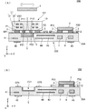
- FIG. 4A is a cross-sectional view of an actuator 302 according to the second embodiment
- FIG. 4B is a cross-sectional view of a base substrate 202 according to the second embodiment.
- the actuator 302 includes a coil substrate 101, a base substrate 202 and a magnet 4.
- the coil substrate 101 and the magnet 4 are the same as those described in the first embodiment.
- the actuator 302 is different from the actuator 301 according to the first embodiment in that the structure of the base substrate is different and the driver IC 2 and the capacitors 7 and 8 are further provided.
- the other configuration of the actuator 302 is substantially the same as the actuator 301.
- the base substrate 202 includes a base 20A, a cavity CV1 formed in the base 20A, a shield conductor 5, and connection electrodes EP1, EP2, EP11, EP12 formed in the base 20A, and conductor patterns 41, 43, 44, 45. , 46, the driver IC 2 and the capacitors 7, 8 and the like.
- the cavity CV1, the shield conductor 5, the connection electrodes EP1 and EP2, and the conductor patterns 41 and 42 are the same as those described in the first embodiment.
- the base 20A has a length in the longitudinal direction (X-axis direction) longer than the base 20 of the base substrate 201 according to the first embodiment.
- the other configuration of the substrate 20A is substantially the same as the substrate 20.
- connection electrodes EP11 and EP12 are rectangular conductor patterns formed on the surface of the base 20A (the upper surface of the base 20A in FIG. 4B).
- the conductor patterns 43 and 44 are conductor patterns formed inside the base material 20A.
- the conductor patterns 45 and 46 are conductor patterns formed on the back surface of the base 20A (the lower surface of the base 20A in FIG. 4B).
- the connection electrodes EP11 and EP12 and the conductor patterns 43, 44, 45 and 46 are conductor patterns of, for example, Cu foil.
- the driver IC 2 is connected to the magnetic sensor 1 and controls the current flowing to the coil L 1 based on the signal from the magnetic sensor 1. As shown in FIG. 4B, the driver IC 2 is mounted on the base 20A. Specifically, the terminals P31 and P32 of the driver IC 2 are connected to the connection electrodes EP11 and EP12 formed on the surface of the base 20A via the conductive bonding material 3.
- the capacitors 7 and 8 are mounted inside the base 20A and arranged in the vicinity of the driver IC 2. Capacitors 7 and 8 are electrically connected between driver IC 2 and the ground of base substrate 202 (substrate 20A). The capacitors 7 and 8 are, for example, chip capacitors.
- the base substrate 202 is provided with a coil drive circuit for driving the coil L1.
- the coil drive circuit includes a driver IC 2, capacitors 7 and 8, a wire connecting the driver IC 2 and the coil L1, a wire connecting the capacitors 7 and 8 and the driver IC 2, and the like.
- the coil substrate 101 is connected to the base substrate 202 via the conductive bonding material 3.
- the driver IC 2 and the capacitors 7 and 8 are mounted on the base substrate 202 on which the coil drive circuit is formed.
- the wiring length of the power supply wiring to the driver IC 2 can be shortened as compared to the case where the driver IC 2 is mounted on the coil substrate 101, so a low loss coil driving circuit can be realized.
- the ground potential of the driver IC 2 can be stabilized more easily than when the driver IC 2 is mounted on the coil substrate 101.
- the wiring length between driver IC 2 and capacitors 7 and 8 (or the grounds of capacitors 7 and 8 and base substrate 202) as compared to the case where capacitors 7 and 8 are mounted on coil substrate 101. Can be shortened). Therefore, the inductance and conductor resistance in the wiring between driver IC 2 and capacitors 7 and 8 (or the inductor and conductor resistance in the wiring between capacitors 7 and 8 and the ground of base substrate 202) can be reduced. The suppression effect of the voltage fluctuation of the driver IC 2 is further enhanced.
- the capacitors 7 and 8 are mounted on the inside of the base substrate 202 (base material 20A).
- the capacitors 7 and 8 may be mounted on the surface of the base substrate 202 (base 20A).
- the number of capacitors is not limited to two, and may be, for example, one or three or more.
- the capacitors 7 and 8 are not limited to chip capacitors (chip components).
- the capacitors 7 and 8 may be, for example, interlayer capacitances formed between conductor patterns facing each other, which are formed in a plurality of insulating base layers.
- the third embodiment shows an example in which a cavity is formed in a coil substrate.
- FIG. 5A is a cross-sectional view of an actuator 303 according to the third embodiment
- FIG. 5B is a cross-sectional view of a coil substrate 103 according to the third embodiment.
- illustration of the magnetic sensor 1 is omitted.
- the actuator 303 includes a coil substrate 103, a base substrate 203 and a magnet 4.
- the magnet 4 is the same as that described in the first embodiment.
- the actuator 303 differs from the actuator 301 according to the first embodiment in that a cavity is formed in the coil substrate. Also, the actuator 303 differs from the actuator 301 in that no cavity is formed in the base substrate. The other configuration of the actuator 303 is substantially the same as that of the actuator 301.
- the coil substrate 103 has a base material 10B, a cavity CV2 formed in the base material 10B, a coil L1, connection electrodes P1, P2, P11A, P12A, a magnetic sensor 1 and the like.
- the coil L1, the connection electrodes P1 and P2, and the magnetic sensor 1 are the same as those described in the first embodiment.
- the base 10B differs from the base 10 described in the first embodiment in that the cavity CV2 is formed.
- the cavity CV2 is an opening formed inward (in the -Z direction) from the second major surface VS2 of the base 10B.
- the planar shape of the cavity CV2 is a shape that matches the planar shape of the magnetic sensor 1.
- the magnetic sensor 1 is disposed in the cavity CV2.
- connection electrodes P11A and P12A are formed on the bottom of the cavity CV2.
- the connection electrodes P11A and P12A are rectangular conductor patterns, for example, a conductor pattern of Cu foil or the like.
- the magnetic sensor 1 is disposed in the cavity CV2 of the substrate 10B and mounted on the bottom of the cavity CV2. Specifically, the terminals P21 and P22 of the magnetic sensor 1 are connected to the connection electrodes P11A and P12A through the conductive bonding material 3, respectively.
- the magnetic sensor 1 is disposed at a position closer to the magnet 4 than the first main surface VS1 (mounting surface) (position in the + Z direction than the mounting surface) ing. Further, in the present embodiment, the magnetic sensor 1 is disposed inside the coil opening of the coil L1.
- the base substrate 203 has a base 20B, a shield conductor 6, connection electrodes EP1 and EP2, and conductor patterns 47 and 48.
- the connection electrodes EP1 and EP2 are the same as those described in the first embodiment.
- the base 20B is different from the base 20 described in the first embodiment in that no cavity is formed.
- the other configuration of the substrate 20B is substantially the same as the substrate 20.
- the conductor patterns 47 and 48 are conductor patterns formed inside the base 20B.
- the conductor patterns 47 and 48 are conductor patterns of, for example, Cu foil.
- the shield conductor 6 is a conductor pattern formed on the surface of the substrate 20B (the upper surface of the substrate 20B in FIG. 5B). As shown in FIG. 5A, the shield conductor 6 is disposed between the magnetic sensor 1 and another conductor pattern (conductor patterns 47 and 48) formed on the base substrate 203.
- the shield conductor 6 is, for example, a conductor pattern such as Cu foil.
- the following effects can be obtained in addition to the effects described in the first embodiment.
- the magnetic sensor 1 is disposed at a position closer to the magnet 4 than the first main surface VS1 (mounting surface). According to this configuration, since the distance between the magnetic sensor 1 and the magnet 4 is short as compared with the case where the magnetic sensor 1 is mounted on the first main surface VS1, the magnetic field detection accuracy of the magnetic sensor 1 with respect to the magnet 4 can be enhanced. it can.
- the magnetic sensor 1 is disposed in the cavity CV2 and disposed inside the coil opening of the coil L1. According to this configuration, the coil substrate on which the magnetic sensor 1 is mounted can be miniaturized (in particular, the thickness in the Z-axis direction can be reduced).
- the magnetic sensor 1 may be mounted on the second main surface VS2 (top surface) of the base 10B. In that case, the distance between the magnetic sensor 1 and the magnet 4 is further shortened, and the magnetic field detection accuracy of the magnetic sensor 1 with respect to the magnet 4 can be further enhanced (see the above (g)).
- the base substrate includes a flexible portion.
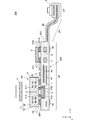
- FIG. 6 is a cross-sectional view of an actuator 304 according to the fourth embodiment.
- the actuator 304 includes a coil substrate 101, a base substrate 204 and a magnet 4.
- the coil substrate 101 is the same as that described in the first and second embodiments.
- the actuator 304 differs from the actuator 302 according to the second embodiment in the configuration of the base substrate.
- the other configuration of the actuator 304 is substantially the same as the actuator 302.
- the base substrate 204 differs from the base substrate 202 in that the base substrate 204 further includes a base 20C, a conductor pattern 49, a connector 9, and the like.
- the base 20C is different from the base 20A described in the second embodiment in that the base 20C includes a flexible portion FP having flexibility and a connection portion CP for external connection connected to the flexible portion FP. .
- the other configuration of the base 20C is substantially the same as that of the base 20A.
- the number of stacked insulating base layers of the flexible portion FP of the base 20C is smaller than the number of stacked insulating base layers of the other portions (the component mounting portion SP and the connection portion CP). Therefore, the flexible portion FP is more flexible and flexible than the other portions.
- the conductor pattern 49 is a conductor pattern formed inside the base material 20C, and is disposed across the flexible portion FP and the connection portion CP.
- the connector 9 is mounted on the surface of the base 20C at the connection portion CP (the upper surface of the base 20C at the connection portion CP in FIG. 6).
- the actuator 304 according to the present embodiment has the following effects in addition to the effects described in the second embodiment.
- the base substrate 204 has a flexible portion FP having flexibility and a connection portion CP for external connection connected to the flexible portion FP.
- the connection portion CP can be easily connected to another substrate or the like by utilizing the flexibility of the flexible portion FP (in a state where the flexible portion FP is bent).
- connection can be made to another substrate or the like through the flexible portion FP having flexibility, when an external force is applied to the connection portion CP (for example, connection to the connection portion CP Even if another substrate or the like is moved), stress is hardly transmitted to the component mounting portion SP, the coil L1, and the magnetic sensor 1. Therefore, it is possible to suppress a change in the characteristics of the actuator (a change in the characteristics accompanying the deformation or the like of the coil L1) caused by the transfer of the stress to the coil L1 and the magnetic sensor 1 and the like.
- the number, the position, the length, and the like of the flexible portion FP and the connection portion CP are not limited to the configuration described in the present embodiment, and can be appropriately changed within the scope of achieving the effects of the present invention.
- base materials 10 and 10B of a coil board and base materials 20, 20A and 20B of a base board showed an example which is a substantially rectangular parallelepiped, it is not limited to this composition .
- the shapes of the base material of the coil substrate and the base material of the base substrate can be appropriately changed in the range where the effects of the present invention are exhibited.
- the planar shape of the substrate is not limited to a rectangle, and may be, for example, a polygon, a circle, an ellipse, a crank, an L shape, a T shape, a Y shape, or the like.
- substrate and the base material of a base substrate showed the example formed by laminating
- the number of laminations of the plurality of insulating base layers forming the base can be appropriately changed in the range where the effects of the present invention are exhibited.
- substrate and the base material of a base substrate are not limited to a laminated body, For example, a single layer may be sufficient.
- the base may be formed by laminating a plurality of insulating base layers made of, for example, a thermosetting resin.
- the coil L1 formed on the coil substrate is a coil of about 4 turns having a winding axis AX along the Z-axis direction.
- the shape, structure, size, number of turns, etc. are not limited to this.
- the number, the shape, the structure and the number of turns of the coil can be appropriately changed within the range where the effects of the present invention are exhibited.
- the coil may be helical, for example, connecting a plurality of looped coil conductor patterns with interlayer connection conductors.
- the outer shape of the coil (the outer shape of the coil viewed from the winding axis AX direction (Z-axis direction)) can be appropriately changed within the range where the effects of the present invention can be exhibited. It may be.
- the winding axis AX of the coil does not have to completely coincide with the Z-axis direction.
- the coil L1 showed the example formed inside the base material of a coil board
- the coil may be composed of, for example, a single coil conductor.
- the coil may be configured to include, for example, two coil conductors respectively formed on both sides of a single insulating base layer.
- the coil may be configured to include, for example, three or more coil conductors respectively formed on three or more of the plurality of insulating base layers.
- the circuit configuration of the coil substrate and the circuit configuration of the base substrate are not limited to the configurations described in the above-described embodiments.
- the circuit configuration of the coil substrate and the circuit configuration of the base substrate can be changed as appropriate within the scope of achieving the effects of the present invention.
- surface mounting components other than the magnetic sensor 1 may be mounted on the coil substrate.
- surface mounting components other than the driver IC 2 and the capacitors 7 and 8 may be mounted on the base substrate.
- a capacitor formed of a conductor pattern or various transmission lines may be formed on the coil substrate and the base substrate.
- substrate and the base material of a base substrate consist of the material of the same main component
- the base of the coil substrate and the base of the base substrate may be composed of different main component materials.
- substrate and the base material of a base substrate consist of the material of the same main component from the point of the effect shown to said (d).
- connection electrodes P1, P2, P11, P11A, P12, and P12A of a coil board showed the example which is a rectangular conductor pattern, it is not limited to this composition.
- connection electrode EP1, EP2, EP11, EP12 of a connection of a base substrate showed the example which is a rectangular conductor pattern, it is not limited to this composition.
- the shape, the number, and the position of the connection electrodes of the coil substrate or the connection electrodes of the base substrate can be appropriately changed within the range where the effects of the present invention are exhibited.
- the number of connection electrodes can be appropriately changed according to the circuit configuration formed on the coil substrate or the base substrate.
- AX coil winding axis
- CP connection portion FP: flexible portion
- SP component mounting portion
- CV1 component mounting portion
- CV1 cavity
- coil P1, P2, P11, P11A, P12, P12A coil substrate connection electrode EP1, EP2 , EP11, EP12 ... connection electrodes for base substrate P21, P22 ... terminals of magnetic sensor P31, P32 ... terminals of driver IC VS1 ... first main surface of coil substrate VS2 ... second main of coil substrate Surface 1 ... Magnetic sensor 2 ...
- Driver IC Reference Signs List 3 conductive joint material 4 magnet 5, shield conductor 7, 8, capacitor 9 connector 10, 10B base material 20, 20A, 20B, 20C of coil substrate base material 31, 32 of base substrate coil Conductors 41, 42, 43, 44, 45, 46, 47, 48, 49 ... conductor patterns 101, 103 ... coil substrates 201, 202, 203, 204 ... base substrates 301, 302, 303, 304 ... actuators
Landscapes
- Engineering & Computer Science (AREA)
- Power Engineering (AREA)
- Microelectronics & Electronic Packaging (AREA)
- Physics & Mathematics (AREA)
- Chemical & Material Sciences (AREA)
- Combustion & Propulsion (AREA)
- Electromagnetism (AREA)
- Manufacturing & Machinery (AREA)
- General Physics & Mathematics (AREA)
- Reciprocating, Oscillating Or Vibrating Motors (AREA)
- Linear Motors (AREA)
Abstract
Un actionneur (301) selon l'invention comprend : un substrat de bobine (101) qui a une bobine (L1) ; un substrat de base (201) dans lequel est formé un circuit de commande de bobine ; et un aimant (4) qui reçoit un champ magnétique généré par la bobine (L1). Un capteur magnétique (1) est monté sur le substrat de bobine (101). Le substrat de bobine (101) sur lequel est monté le capteur magnétique (1) est couplé au substrat de base (201) par l'intermédiaire de matériaux de jonction conducteurs (3).
Priority Applications (3)
| Application Number | Priority Date | Filing Date | Title |
|---|---|---|---|
| JP2019532470A JP7082622B2 (ja) | 2017-07-24 | 2018-07-03 | アクチュエータ、およびアクチュエータの製造方法 |
| CN201890000987.9U CN211296528U (zh) | 2017-07-24 | 2018-07-03 | 致动器 |
| US16/718,279 US11588382B2 (en) | 2017-07-24 | 2019-12-18 | Actuator and method of manufacturing actuator |
Applications Claiming Priority (2)
| Application Number | Priority Date | Filing Date | Title |
|---|---|---|---|
| JP2017142828 | 2017-07-24 | ||
| JP2017-142828 | 2017-07-24 |
Related Child Applications (1)
| Application Number | Title | Priority Date | Filing Date |
|---|---|---|---|
| US16/718,279 Continuation US11588382B2 (en) | 2017-07-24 | 2019-12-18 | Actuator and method of manufacturing actuator |
Publications (1)
| Publication Number | Publication Date |
|---|---|
| WO2019021764A1 true WO2019021764A1 (fr) | 2019-01-31 |
Family
ID=65040576
Family Applications (1)
| Application Number | Title | Priority Date | Filing Date |
|---|---|---|---|
| PCT/JP2018/025218 Ceased WO2019021764A1 (fr) | 2017-07-24 | 2018-07-03 | Actionneur et procédé de fabrication d'actionneur |
Country Status (4)
| Country | Link |
|---|---|
| US (1) | US11588382B2 (fr) |
| JP (1) | JP7082622B2 (fr) |
| CN (1) | CN211296528U (fr) |
| WO (1) | WO2019021764A1 (fr) |
Cited By (2)
| Publication number | Priority date | Publication date | Assignee | Title |
|---|---|---|---|---|
| WO2023276562A1 (fr) * | 2021-06-30 | 2023-01-05 | 株式会社村田製作所 | Module d'entraînement et dispositif électronique |
| WO2023021908A1 (fr) * | 2021-08-19 | 2023-02-23 | 株式会社村田製作所 | Module de substrat, module de pilotage et appareil électronique |
Families Citing this family (1)
| Publication number | Priority date | Publication date | Assignee | Title |
|---|---|---|---|---|
| JP7159894B2 (ja) * | 2019-02-05 | 2022-10-25 | 日本電信電話株式会社 | 擬似力覚提示装置 |
Citations (6)
| Publication number | Priority date | Publication date | Assignee | Title |
|---|---|---|---|---|
| JPS4828605B1 (fr) * | 1968-04-06 | 1973-09-03 | ||
| JPS53147219A (en) * | 1977-05-27 | 1978-12-21 | Nippon Telegr & Teleph Corp <Ntt> | Brushless direct current linear motor |
| JPH08140333A (ja) * | 1994-11-07 | 1996-05-31 | Nippon Thompson Co Ltd | リニア直流モータ |
| JPH11235067A (ja) * | 1997-06-19 | 1999-08-27 | Eaton Corp | モータへの電力供給制御システム |
| WO2004047252A1 (fr) * | 2002-11-18 | 2004-06-03 | Seiko Epson Corporation | Stator de moteur sans balai, moteur sans balai equipe de ce stator et structure de bobine |
| JP2015180157A (ja) * | 2014-03-19 | 2015-10-08 | 日立オートモティブシステムズ株式会社 | 電動モータの電子回路装置 |
Family Cites Families (12)
| Publication number | Priority date | Publication date | Assignee | Title |
|---|---|---|---|---|
| CA971365A (en) | 1971-08-19 | 1975-07-22 | George A. Lane | Pyrotechnic composition for inflation of passive restraint systems |
| JP3167044B2 (ja) * | 1992-02-13 | 2001-05-14 | 日本トムソン株式会社 | 直流リニアモータ及びこれを具備した直動ユニット |
| JP2007020266A (ja) * | 2005-07-06 | 2007-01-25 | Mitsuba Corp | 電動機 |
| US7816905B2 (en) * | 2008-06-02 | 2010-10-19 | Allegro Microsystems, Inc. | Arrangements for a current sensing circuit and integrated current sensor |
| CH708052B1 (de) * | 2013-05-07 | 2016-09-15 | Melexis Technologies Nv | Vorrichtung zur Strommessung. |
| WO2015079773A1 (fr) * | 2013-11-28 | 2015-06-04 | 株式会社村田製作所 | Électroaimant, procédé d'entraînement d'objectif, et procédé de fabrication d'électroaimant |
| TWI518396B (zh) | 2014-12-19 | 2016-01-21 | 台灣東電化股份有限公司 | 薄型鏡頭模組 |
| JP6459504B2 (ja) | 2014-12-25 | 2019-01-30 | ミツミ電機株式会社 | レンズ駆動装置、カメラモジュール、及びカメラ搭載装置 |
| JP2016191849A (ja) | 2015-03-31 | 2016-11-10 | ミツミ電機株式会社 | レンズ駆動装置、カメラモジュール、及びカメラ搭載装置 |
| JP6585912B2 (ja) * | 2015-03-31 | 2019-10-02 | 旭化成エレクトロニクス株式会社 | カメラモジュール |
| US9869729B1 (en) * | 2016-08-30 | 2018-01-16 | Infineon Technologies Ag | Magnetic field sensor circuit in package with means to add a signal from a coil |
| US10340444B2 (en) * | 2016-12-28 | 2019-07-02 | Rohm Co., Ltd. | Semiconductor element with hall element and sealing resin |
-
2018
- 2018-07-03 CN CN201890000987.9U patent/CN211296528U/zh active Active
- 2018-07-03 WO PCT/JP2018/025218 patent/WO2019021764A1/fr not_active Ceased
- 2018-07-03 JP JP2019532470A patent/JP7082622B2/ja active Active
-
2019
- 2019-12-18 US US16/718,279 patent/US11588382B2/en active Active
Patent Citations (6)
| Publication number | Priority date | Publication date | Assignee | Title |
|---|---|---|---|---|
| JPS4828605B1 (fr) * | 1968-04-06 | 1973-09-03 | ||
| JPS53147219A (en) * | 1977-05-27 | 1978-12-21 | Nippon Telegr & Teleph Corp <Ntt> | Brushless direct current linear motor |
| JPH08140333A (ja) * | 1994-11-07 | 1996-05-31 | Nippon Thompson Co Ltd | リニア直流モータ |
| JPH11235067A (ja) * | 1997-06-19 | 1999-08-27 | Eaton Corp | モータへの電力供給制御システム |
| WO2004047252A1 (fr) * | 2002-11-18 | 2004-06-03 | Seiko Epson Corporation | Stator de moteur sans balai, moteur sans balai equipe de ce stator et structure de bobine |
| JP2015180157A (ja) * | 2014-03-19 | 2015-10-08 | 日立オートモティブシステムズ株式会社 | 電動モータの電子回路装置 |
Cited By (5)
| Publication number | Priority date | Publication date | Assignee | Title |
|---|---|---|---|---|
| WO2023276562A1 (fr) * | 2021-06-30 | 2023-01-05 | 株式会社村田製作所 | Module d'entraînement et dispositif électronique |
| JPWO2023276562A1 (fr) * | 2021-06-30 | 2023-01-05 | ||
| JP7306604B2 (ja) | 2021-06-30 | 2023-07-11 | 株式会社村田製作所 | 駆動モジュール及び電子機器 |
| WO2023021908A1 (fr) * | 2021-08-19 | 2023-02-23 | 株式会社村田製作所 | Module de substrat, module de pilotage et appareil électronique |
| JPWO2023021908A1 (fr) * | 2021-08-19 | 2023-02-23 |
Also Published As
| Publication number | Publication date |
|---|---|
| US20200127549A1 (en) | 2020-04-23 |
| CN211296528U (zh) | 2020-08-18 |
| JP7082622B2 (ja) | 2022-06-08 |
| US11588382B2 (en) | 2023-02-21 |
| JPWO2019021764A1 (ja) | 2020-02-06 |
Similar Documents
| Publication | Publication Date | Title |
|---|---|---|
| US20250378993A1 (en) | Coil component having resin walls | |
| JP5915821B2 (ja) | 電磁石の製造方法、および、電磁石 | |
| JP2015088753A (ja) | コイル部品とその製造方法、コイル部品内蔵基板、及びこれを含む電圧調節モジュール | |
| CN205080957U (zh) | 电感元件及电子设备 | |
| WO2019021764A1 (fr) | Actionneur et procédé de fabrication d'actionneur | |
| JP6516017B2 (ja) | Lc複合デバイス、プロセッサおよびlc複合デバイスの製造方法 | |
| CN210641154U (zh) | 多层基板 | |
| US11202371B2 (en) | Multilayer substrate | |
| WO2018174133A1 (fr) | Substrat multicouche, actionneur et procédé de production de substrat multicouche | |
| CN106449550B (zh) | 芯片封装模块 | |
| CN209805646U (zh) | 致动器 | |
| CN209570686U (zh) | 磁元件 | |
| JP4992735B2 (ja) | 電子部品 | |
| JP6610623B2 (ja) | アクチュエータ | |
| JP6638825B2 (ja) | 多層基板 | |
| CN211152314U (zh) | 电元件、致动器以及通信装置 |
Legal Events
| Date | Code | Title | Description |
|---|---|---|---|
| 121 | Ep: the epo has been informed by wipo that ep was designated in this application |
Ref document number: 18838673 Country of ref document: EP Kind code of ref document: A1 |
|
| ENP | Entry into the national phase |
Ref document number: 2019532470 Country of ref document: JP Kind code of ref document: A |
|
| NENP | Non-entry into the national phase |
Ref country code: DE |
|
| 122 | Ep: pct application non-entry in european phase |
Ref document number: 18838673 Country of ref document: EP Kind code of ref document: A1 |