WO2019021835A1 - Élément conducteur de panneau tactile et panneau tactile - Google Patents
Élément conducteur de panneau tactile et panneau tactile Download PDFInfo
- Publication number
- WO2019021835A1 WO2019021835A1 PCT/JP2018/026257 JP2018026257W WO2019021835A1 WO 2019021835 A1 WO2019021835 A1 WO 2019021835A1 JP 2018026257 W JP2018026257 W JP 2018026257W WO 2019021835 A1 WO2019021835 A1 WO 2019021835A1
- Authority
- WO
- WIPO (PCT)
- Prior art keywords
- mesh
- conductive layer
- touch panel
- layer
- straight line
- Prior art date
- Legal status (The legal status is an assumption and is not a legal conclusion. Google has not performed a legal analysis and makes no representation as to the accuracy of the status listed.)
- Ceased
Links
Images




Classifications
-
- G—PHYSICS
- G06—COMPUTING OR CALCULATING; COUNTING
- G06F—ELECTRIC DIGITAL DATA PROCESSING
- G06F3/00—Input arrangements for transferring data to be processed into a form capable of being handled by the computer; Output arrangements for transferring data from processing unit to output unit, e.g. interface arrangements
- G06F3/01—Input arrangements or combined input and output arrangements for interaction between user and computer
- G06F3/03—Arrangements for converting the position or the displacement of a member into a coded form
- G06F3/041—Digitisers, e.g. for touch screens or touch pads, characterised by the transducing means
- G06F3/044—Digitisers, e.g. for touch screens or touch pads, characterised by the transducing means by capacitive means
- G06F3/0445—Digitisers, e.g. for touch screens or touch pads, characterised by the transducing means by capacitive means using two or more layers of sensing electrodes, e.g. using two layers of electrodes separated by a dielectric layer
-
- G—PHYSICS
- G06—COMPUTING OR CALCULATING; COUNTING
- G06F—ELECTRIC DIGITAL DATA PROCESSING
- G06F3/00—Input arrangements for transferring data to be processed into a form capable of being handled by the computer; Output arrangements for transferring data from processing unit to output unit, e.g. interface arrangements
- G06F3/01—Input arrangements or combined input and output arrangements for interaction between user and computer
- G06F3/03—Arrangements for converting the position or the displacement of a member into a coded form
- G06F3/041—Digitisers, e.g. for touch screens or touch pads, characterised by the transducing means
- G06F3/044—Digitisers, e.g. for touch screens or touch pads, characterised by the transducing means by capacitive means
- G06F3/0446—Digitisers, e.g. for touch screens or touch pads, characterised by the transducing means by capacitive means using a grid-like structure of electrodes in at least two directions, e.g. using row and column electrodes
-
- G—PHYSICS
- G06—COMPUTING OR CALCULATING; COUNTING
- G06F—ELECTRIC DIGITAL DATA PROCESSING
- G06F3/00—Input arrangements for transferring data to be processed into a form capable of being handled by the computer; Output arrangements for transferring data from processing unit to output unit, e.g. interface arrangements
- G06F3/01—Input arrangements or combined input and output arrangements for interaction between user and computer
- G06F3/03—Arrangements for converting the position or the displacement of a member into a coded form
- G06F3/041—Digitisers, e.g. for touch screens or touch pads, characterised by the transducing means
- G06F3/044—Digitisers, e.g. for touch screens or touch pads, characterised by the transducing means by capacitive means
- G06F3/0448—Details of the electrode shape, e.g. for enhancing the detection of touches, for generating specific electric field shapes, for enhancing display quality
-
- G—PHYSICS
- G06—COMPUTING OR CALCULATING; COUNTING
- G06F—ELECTRIC DIGITAL DATA PROCESSING
- G06F3/00—Input arrangements for transferring data to be processed into a form capable of being handled by the computer; Output arrangements for transferring data from processing unit to output unit, e.g. interface arrangements
- G06F3/01—Input arrangements or combined input and output arrangements for interaction between user and computer
- G06F3/03—Arrangements for converting the position or the displacement of a member into a coded form
- G06F3/041—Digitisers, e.g. for touch screens or touch pads, characterised by the transducing means
- G06F3/047—Digitisers, e.g. for touch screens or touch pads, characterised by the transducing means using sets of wires, e.g. crossed wires
-
- G—PHYSICS
- G06—COMPUTING OR CALCULATING; COUNTING
- G06F—ELECTRIC DIGITAL DATA PROCESSING
- G06F2203/00—Indexing scheme relating to G06F3/00 - G06F3/048
- G06F2203/041—Indexing scheme relating to G06F3/041 - G06F3/045
- G06F2203/04112—Electrode mesh in capacitive digitiser: electrode for touch sensing is formed of a mesh of very fine, normally metallic, interconnected lines that are almost invisible to see. This provides a quite large but transparent electrode surface, without need for ITO or similar transparent conductive material
Definitions
- the present invention relates to a conductive member for a touch panel and a touch panel having a mesh pattern composed of a plurality of mesh cells made of metal fine wires, and in particular, a conductive member for a touch panel in which the intersections of meshes are less visible and which maintain detection sensitivity
- the present invention relates to a touch panel in which mesh intersection points are hard to be visually recognized.
- a touch panel having a mesh electrode using thin metal wires as a detection electrode of a touch can have low resistance and low parasitic capacitance with respect to a touch panel using a transparent electrode made of ITO (Indium Tin Oxide) as a detection electrode It is.
- ITO Indium Tin Oxide
- Patent Document 1 describes a micro wire pattern having offset cross points such that the cross points have three cross elements. In Patent Document 1, by setting the offset intersection point, the intersection point is made smaller to reduce the visibility of the intersection point.
- each branch point of the conductive mesh is formed by a plurality of line segments extending between two intersection points to define an opening area, and one intersection point of a reference mesh pattern in which the opening areas are periodically arranged. It is located at a position displaced from the one intersection by a length that is above or below a predetermined length, and each connection element of the conductive mesh corresponds to two intersections located at both ends of one line segment. Between the two diverging points.
- the touch panel sensor of Patent Document 3 includes a detection electrode including a conductive mesh that defines a plurality of opening regions.
- the conductive mesh is formed of conductive thin wires arranged in a pattern defining hexagonal opening regions arranged at a constant pitch in each of the first direction and the second direction orthogonal to each other.
- Patent Document 1 although the visibility is improved by setting the intersections of the microwires as offset intersections, the improvement of the visibility is not sufficient. Moreover, in Patent Document 2 and Patent Document 3, although both moire and light and shade unevenness are made inconspicuous, it is not sufficient. Under the present circumstances, when the above-mentioned thin metal wire is used, it can not be said that the countermeasure regarding visibility, such as a thin metal wire is visible, is enough. In particular, in a mesh electrode touch panel using thin metal wires, in the case of mesh electrodes having a thickening at which the mesh intersection points become thick, there is a problem of visibility of the thin metal wires.
- intersection weight index is the five mesh intersection points. It is an average value.
- the line width of the thin metal wire is measured at the midpoint between mesh intersection points (mid point of the side of the mesh cell).
- the line width of the thin metal wire is an average value of the line widths of lines extending from mesh intersections. If the mesh shape of the mesh pattern is a quadrilateral, it is the average value of the line widths of the four thin metal wires extending from the intersection.
- the object of the present invention is to solve the problems based on the above-mentioned prior art, and to provide a conductive member for a touch panel and a touch panel excellent in visibility.
- the present invention is a conductive member for a touch panel, having a transparent insulating substrate and a first conductive layer formed on the transparent insulating substrate, wherein the first conductive layer has a plurality of apexes. It has a first mesh pattern composed of a plurality of first mesh cells in a closed shape connected by metal thin wires, and a directional component in which the apexes of the plurality of first mesh cells are aligned in a straight line is 1 or less.
- the conductive member for a touch panel is provided.
- the direction component in which the vertex of the several 1st mesh cell of a 1st conductive layer is located in a straight line is one.
- the closed shape of the first mesh pattern is an N-gon, preferably N is 3 or more, and the N-gon is more preferably a tetragon.
- a second mesh pattern composed of the plurality of second mesh cells, the direction component in which the apexes of the plurality of second mesh cells are aligned in a straight line is 1 or less, and the first conductive layer and the second conductive layer are overlapped When viewed from the stacking direction, it is preferable that a plurality of vertices of the second mesh cell be arranged in the corresponding first mesh cells.
- the direction component in which the apexes of the plurality of first mesh cells in the layer are linearly aligned intersect with the direction component in which the apexes of the plurality of second mesh cells in the second conductive layer are linearly arranged.
- the closed shape of the second mesh pattern is an S-gon, it is preferable that S be 3 or more, and it is more preferable that the S-gon be a tetragon.
- the present invention also provides a touch panel characterized by having the above-described touch panel conductive member of the present invention.
- the electroconductive member for touchscreens and the touchscreen which were excellent in visibility can be provided.
- excellent visibility can be obtained.
- Angles such as “specifically expressed angles”, “parallel”, “vertical” and “orthogonal” include error ranges generally accepted in the relevant technical field unless otherwise noted. Also, “identical” includes an error range generally accepted in the relevant technical field.
- transparent means that the light transmittance is 40% or more, preferably 80% or more, more preferably 90% or more in the visible light wavelength range of 380 to 780 nm. The light transmittance is measured, for example, using “a method of determining total light transmittance and total light reflectance of plastic” defined in JIS (Japanese Industrial Standard) K 7375: 2008.
- FIG. 1 is a schematic cross-sectional view showing an example of the configuration of a touch panel having a conductive member for a touch panel according to an embodiment of the present invention
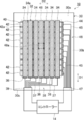
- FIG. 2 is a schematic diagram showing the configuration of a touch panel having a conductive member for a touch panel according to an embodiment of the present invention.
- the touch panel 10 shown in FIG. 1 has a touch panel conductive member 11.
- the touch panel conductive member 11 shown in FIG. 1 has a transparent insulating substrate 30 and a first conductive layer 32 and a second conductive layer 40 formed on the transparent insulating substrate 30, but at least the first conductive layer.
- One of 32 and the second conductive layer 40 may be provided.
- a transparent layer 15 and a cover layer 12 are stacked on the touch panel conductive member 11.
- the surface 12 a of the cover layer 12 is a touch surface of the touch panel 10 and is an operation surface.
- a touch surface is a surface which detects contact of members, such as a finger or a stylus pen.
- the touch panel conductive member 11 is connected to a controller 14 (see FIG. 2).
- the touch panel 10 is configured by the touch panel conductive member 11, the cover layer 12, and the controller 14.
- the touch panel 10 is provided on the display panel 20 via, for example, a transparent layer 18.
- the surface 12 a of the cover layer 12 is a viewing surface of the display object (not shown) displayed in the display area (not shown) of the display panel 20.
- the touch panel 10 and the display panel 20 constitute a display device.
- the controller 14 is configured of a known one used for detection of a capacitive touch sensor.
- the controller 14 detects the position at which the capacitance has changed due to the contact of a finger or the like on the surface 12 a of the cover layer 12.
- the touch panel 10 includes the touch panel conductive member 11.
- the touch panel 10 including the touch panel conductive member 11 is suitably used as a capacitive touch panel.
- the capacitive touch panel includes a mutual capacitive touch panel and a self-capacitive touch panel, but is particularly suitable as a mutual capacitive touch panel.
- the cover layer 12 functions as a protective layer of the touch panel conductive member 11.
- the configuration of the cover layer 12 is not particularly limited.
- glass such as plate glass and tempered glass, or acrylic resin such as polycarbonate (PC), polyethylene terephthalate (PET), or polymethyl methacrylate resin (PMMA) is used.
- PC polycarbonate
- PET polyethylene terephthalate
- PMMA polymethyl methacrylate resin
- the surface 12 a of the cover layer 12 is a touch surface as described above, a hard coat layer may be provided on the surface 12 a as required.
- the thickness of the cover layer 12 is 0.1 to 1.3 mm, preferably 0.1 to 0.7 mm.
- the configuration of the transparent layer 18 is not particularly limited as long as the transparent layer 18 is optically transparent and has an insulating property, and the touch panel conductive member 11 and the display panel 20 can be stably fixed.
- the transparent layer 18 for example, optically clear adhesive (OCA, Optical Clear Adhesive) and optically clear resin (OCR, Optical Clear Resin) such as UV (Ultra Violet) curing resin can be used.
- OCA optically clear adhesive
- OCR optically clear Resin
- the transparent layer 18 may be partially hollow.
- a gap may be provided on the display panel 20 to separate the conductive member 11 for a touch panel. This gap is also referred to as an air gap.
- the configuration of the transparent layer 15 is not particularly limited as long as the transparent layer 15 is optically transparent and has an insulating property, and the touch panel conductive member 11 and the cover layer 12 can be stably fixed. is not.
- the same transparent layer 15 as the transparent layer 18 can be used.
- the display panel 20 includes a display area (not shown), and is, for example, a liquid crystal display panel.
- the display panel 20 is not limited to a liquid crystal display panel, and may be an organic electro luminescence (EL) display panel.
- the display device is an electronic device, but the electronic device is not limited to the display device.
- the above-mentioned display apparatus is mentioned, for example. Specific examples of the electronic device include mobile phones, smart phones, portable information terminals, car navigation systems, tablet terminals, laptop personal computers, and desktop personal computers.
- the touch panel conductive member 11 is used for a capacitive touch sensor, in particular, a mutual capacitive touch sensor.
- the first conductive layer 32 is provided on the surface 30 a of the transparent insulating substrate 30.
- the second conductive layer 40 is provided on the back surface 30 b of the transparent insulating substrate 30.
- the first conductive layer 32 is formed directly on the surface 30a of the transparent insulating substrate 30, and the second conductive layer 40 is formed directly on the back surface 30b.
- an underlayer an undercoat layer
- an adhesion enhancing layer for improving the adhesion between the electrode layer and the transparent insulating substrate
- One or more other functional layers may be provided.
- the cover layer 12 is stacked on the surface 30a of the transparent insulating substrate 30, and the surface 30a side of the transparent insulating substrate 30 is the touch surface side, that is, the side for detecting contact.
- the first conductive layer 32 includes the detection electrodes of the touch panel, and the thin metal wires 52 of the first conductive layer 32 constitute a plurality of first electrodes 34 which are detection electrodes of the touch panel.
- the first electrode 34 is a long strip electrode extending parallel to the first direction D1.
- a plurality of first electrodes 34 are arranged in parallel in a second direction D2 orthogonal to the first direction D1 and spaced apart from each other, and electrically insulated from each other.
- the first conductive layer 32 has a first pad 36 electrically connected to the fine metal wire 52 (see FIG. 1) constituting the first electrode 34.
- the first peripheral wiring 37 is electrically connected to the first pad 36 of each first electrode 34.
- the respective first peripheral wires 37 are arranged close to each other, and the plurality of first peripheral wires 37 are individually connected to terminals for connecting to the controller 14, and these terminals are formed on the transparent insulating substrate 30.
- the plurality of first peripheral wirings 37 are collectively referred to as a first peripheral wiring section 38.
- the second conductive layer 40 includes the detection electrode of the touch panel, and the metal thin wires 52 of the second conductive layer 40 constitute a plurality of second electrodes 42.
- the second electrode 42 is a long strip electrode extending parallel to the second direction D2.
- a plurality of second electrodes 42 are arranged in parallel in a first direction D1 orthogonal to the second direction D2, spaced apart from one another, and electrically insulated from one another.
- the second conductive layer 40 has, for example, the same configuration as that of the first conductive layer 32 described above.
- the second conductive layer 40 has a second pad 44 electrically connected to the metal thin wire 52 (see FIG. 1) constituting the second electrode 42.
- the second peripheral wiring 45 is electrically connected to the second pad 44 of each second electrode 42.
- the respective second peripheral wires 45 are arranged close to each other.
- the plurality of second peripheral wires 45 are individually connected to terminals for connection to the controller 14, and the terminals are grouped into one terminal connection region 47 at one side 30 c of the transparent insulating substrate 30.
- the plurality of second peripheral wires 45 are collectively referred to as a second peripheral wire portion 46.
- the first conductive layer 32 and the second conductive layer 40 are electrically insulated by the transparent insulating substrate 30 and are spaced apart. In addition, being spaced apart and arrange
- the second electrode 42 is disposed to intersect the first electrode 34 of the first conductive layer 32 at least in part. A portion where the first electrode 34 and the second electrode 42 overlap is a crossing portion 48 a.
- the first conductive layer 32 is provided on the surface 30a of one transparent insulating substrate 30, and the second conductive layer 40 is provided on the back surface 30b, so that the transparent insulating substrate 30 shrinks. Also, the displacement of the positional relationship between the first conductive layer 32 and the second conductive layer 40 can be reduced.
- the first peripheral wiring 37 and the second peripheral wiring 45 are formed of, for example, a conductor wiring.
- a sensing area 48 which is a sensor area for detecting a touch shown in FIG.
- the sensing area 48 is an area in which detection of a touch with a finger or the like, that is, a touch can be performed in the capacitive touch panel.
- the touch panel conductive member 11 is disposed on the display area of the display panel 20, and the sensing area 48 is disposed so as to overlap the pixel display area on which the display image of the display panel 20 (see FIG. 1) is displayed. .
- the sensing area 48 may be wider than the pixel display area.
- a decorative layer (not shown) having a light shielding function is provided. By covering the first peripheral wiring portion 38 and the second peripheral wiring portion 46 with the decorative layer, the first peripheral wiring portion 38 and the second peripheral wiring portion 46 are made invisible.
- the configuration of the decorative layer is not particularly limited as long as the first peripheral wiring portion 38 and the second peripheral wiring portion 46 can be made invisible, and a known decorative layer can be used. .
- various printing methods such as screen printing, gravure printing and offset printing, transfer methods, and evaporation methods can be used, and the cover layer 12 is formed. It may be formed directly on the peripheral wiring portion 38 and the second peripheral wiring portion 46.
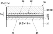
- the touch panel 10 is not particularly limited to that shown in FIG. 1 and FIG. 2, and for example, like the touch panel 10 shown in FIG. 3, the first conductive layer 32 is formed on the transparent insulating substrate 30,
- the insulating film 31 is formed on the first conductive layer 32
- the second conductive layer 40 is formed on the insulating film 31
- the first conductive layer 32 and the second conductive layer 40 are laminated via the insulating film 31. It may be a laminated structure.
- the transparent insulating substrate 30 doubles as the cover layer 12, and the first conductive layer 32 is disposed on the touch surface side.
- a transparent layer 49 covering the second conductive layer 40 is formed on the insulating film 31 and provided on the display panel 20 via the transparent layer 18.
- the insulating film 31 may have the same configuration as the transparent insulating substrate 30 or may have a different configuration.
- the transparent layer 49 can be the same as the transparent layer 18 described above. In the configuration shown in FIG. 3, the stacking direction in which the first conductive layer 32 and the second conductive layer 40 are stacked is the same as the perpendicular direction Dn.
- the touch panel conductive member 11 is provided with the first conductive layer 32 on one transparent insulating substrate 30, and another transparent insulating substrate (not shown).
- another conductive member for a touch panel (not shown) provided with the second conductive layer 40 may be laminated via an optically transparent adhesive. That is, the first conductive layer 32 and the second conductive layer 40 may be insulated and disposed to face each other.
- FIG. 4 is a schematic view showing a first example of the first conductive layer and the second conductive layer of the conductive member for a touch panel according to the embodiment of the present invention
- FIG. 5 is a schematic view of the conductive member for the touch panel according to the embodiment of the present invention
- FIG. 6 shows the 3rd example of the 1st electric conduction layer of the electric conduction member for touch panels of the embodiment of the present invention, and the 2nd electric conduction layer
- FIG. 4 is a schematic view showing a first example of the first conductive layer and the second conductive layer of the conductive member for a touch panel according to the embodiment of the present invention
- FIG. 5 is a schematic view of the conductive member for the touch panel according to the embodiment of the present invention
- Drawing 6 shows the 3rd example of the 1st electric conduction layer of the electric conduction member for touch panels of the embodiment of the present invention, and the 2nd electric conduction layer
- FIG. 4 is a schematic view showing a first example of the first conductive layer and the
- FIG. 7 is a schematic view showing a fourth example of the first conductive layer and the second conductive layer of the conductive member for a touch panel according to the embodiment of the present invention
- FIG. 8 is a diagram showing a fourth example of the conductive member for a touch panel according to the embodiment of the present invention It is a schematic diagram which shows the 5th example of 1 conductive layer and a 2nd conductive layer.
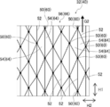
- FIGS. 4 to 8 are diagrams showing patterns of the first conductive layer 32 and the second conductive layer 40 superimposed and viewed in plan view. Further, in FIG. 4 to FIG. 8, the reference symbol H1 indicates the extending direction of the first electrode 34 of the first conductive layer 32 and the second electrode 42 of the second conductive layer 40.
- the symbol H 2 indicates a direction orthogonal to the extending direction of the first electrode 34 of the first conductive layer 32 and the second electrode 42 of the second conductive layer 40.
- the extending direction H1 is the above-mentioned first direction D1 if it is the first conductive layer 32, and it is the above-mentioned second direction D2 if it is the second conductive layer 40.
- the black circles shown in FIGS. 4 to 8 indicate the apex 50 of the first mesh cell 54 and the apex 60 of the second mesh cell 64.
- the first conductive layer 32 has a first mesh pattern 56 formed by connecting a plurality of first mesh cells 54 in a closed shape in which a plurality of apexes 50 are connected by metal thin wires 52. .
- the first mesh cell 54 shown in FIG. 4 is a quadrilateral.
- the apex 50 is a region in which at least two metal thin wires 52 are in contact, and, for example, the metal thin wires 52 are crossed.
- the first conductive layer 32 has a direction component in which the apexes 50 of the plurality of first mesh cells 54 are aligned in a straight line is 1 or less.
- the direction component in which the vertexes of mesh cells are aligned in a straight line is 1 or less, and the direction component in which the vertices of mesh cells are aligned in a straight line is 0 or 1. It is preferable that the direction component in which the apexes of the mesh cells of the first conductive layer 32 are aligned in a straight line is one. This is because noise is suppressed when the direction component in which the vertexes of the mesh cells are aligned in a straight line is 1.
- the presence of noise may cause an impression such as graininess or graininess when a viewer looks at a touch panel or a conductive member for a touch panel.
- the direction component in which the vertexes of the mesh cells are aligned in a straight line will be described in detail later.
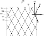
- the mesh pattern 100 shown in FIG. 13 is a fixed mesh pattern in which mesh cells 102 of the same rhombus are repeatedly arranged.
- the direction component of the mesh cell apex is 4 and the direction component of the mesh cell apex is G1, G2 and G3. , G4.
- the apexes 104 of the mesh cells 102 are all arranged in a straight line, the apexes 104 of the mesh cells 102 are noticeable and the visibility is poor.
- the vertices of mesh cells are also called mesh intersections.
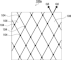
- the arrangement of the apexes 104 of the mesh cell 106 has directions G5 and G6 of the direction components in which the direction components of the mesh cell apex are aligned in a straight line 2 and the apexes of the mesh cell are aligned in a straight line . Even in this case, since the apexes 104 of the mesh cells 106 are all aligned in a straight line, the apexes 104 of the mesh cells 102 are noticeable and the visibility is poor.
- the configuration of the second conductive layer 40 is not particularly limited, but is preferably the same as that of the first conductive layer 32.
- the second conductive layer 40 has a second mesh pattern 66 configured by connecting a second mesh cell 64 having a closed shape in which a plurality of apexes 60 are connected by a thin metal wire 52.
- the second mesh cell 64 shown in FIG. 4 is a quadrilateral.
- the second conductive layer 40 preferably has a direction component in which the apexes 60 of the plurality of second mesh cells 64 are aligned in a straight line is 1 or less.
- the vertex 60 is the same as the vertex 50, and is a region in which at least two metal thin wires 52 are in contact with each other. For example, the metal thin wires 52 are crossed.
- the first conductive layer 32 and the second conductive layer 40 shown in FIG. 4 each have a direction component in which the apexes of mesh cells are aligned in a straight line, and the direction G1 of the direction components in which the apexes of mesh cells are aligned in a straight line is H2 Parallel to Further, as shown in FIG. 5, in the first conductive layer 32, the direction component in which the apexes of mesh cells are aligned in a straight line may be zero. In this case, as will be described in detail later, the vertex 50 is not arranged on a straight line across the four or more first mesh cells 54.
- the first mesh cell 54 even if the vertex 50 is disposed on a straight line, there is no straight line parallel to the straight line. Also in the example shown in FIG. 5, the first mesh cell 54 is a quadrilateral. In FIG. 5, in the second conductive layer 40 as well, the direction component in which the apexes of mesh cells are aligned in a straight line is zero. The vertex 60 is not arranged on a straight line over four or more second mesh cells 64. Further, in the four or more second mesh cells 64, even if the apex 60 is disposed on a straight line, there is no straight line parallel to this straight line. Also in the example shown in FIG. 5, the second mesh cell 64 is a quadrilateral.
- the first conductive layer 32 shown in FIG. 6 has a direction component in which the vertexes of the mesh cells are aligned in a straight line
- the direction G2 of the direction component in which the vertexes of the mesh cells are aligned in a straight line is parallel to the extending direction H1.
- the first conductive layer 32 shown in FIG. 6 has the same configuration as that of the first conductive layer 32 shown in FIG. 4 except that the direction components of the mesh cell apexes are aligned in a straight line are different. Therefore, detailed description of the first conductive layer 32 shown in FIG. 6 will be omitted.
- the second conductive layer 40 shown in FIG. 6 also has the same configuration as that of the second conductive layer 40 shown in FIG.
- the first mesh cell 54 of the first conductive layer 32 and the second mesh cell 64 of the second conductive layer 40 shown in FIG. 6 are both square.
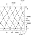
- the first conductive layer 32 shown in FIG. 7 has a direction component in which the vertexes of the mesh cells are aligned in a straight line, and the direction G1 of the direction component in which the vertexes of the mesh cells are aligned in a straight line is perpendicular to the extending direction H1. is there.
- the first conductive layer 32 shown in FIG. 7 has the same configuration as that of the first conductive layer 32 shown in FIG. 4 except that the shape of the first mesh cell 54 is triangular. Therefore, detailed description of the first conductive layer 32 shown in FIG. 7 will be omitted.
- the first conductive layer 32 is provided with fine metal wires 52 which pass through the apex 50 and are parallel to the direction H2.
- the second conductive layer 40 has the same configuration as that of the second conductive layer 40 shown in FIG. 4 except that the shape of the second mesh cell 64 is triangular. Therefore, detailed description of the second conductive layer 40 shown in FIG. 7 will be omitted.
- the second conductive layer 40 is provided with fine metal wires 52 which pass through the apex 60 and are parallel to the direction H2.
- the first mesh cell 54 of the first conductive layer 32 and the second mesh cell 64 of the second conductive layer 40 shown in FIG. 7 are both triangular.
- the first conductive layer 32 shown in FIG. 8 has a direction component in which the apexes of mesh cells are aligned in a straight line, and the direction G2 of the direction components in which the apexes of mesh cells are aligned in a straight line is parallel to the extending direction H1.
- the first conductive layer 32 shown in FIG. 8 is different from the first conductive layer 32 shown in FIG. 4 in that the direction components of the mesh cell's apexes are aligned in a straight line and the shape of the first mesh cell 54 is three.
- the configuration is the same except that it is a square. Therefore, detailed description of the first conductive layer 32 shown in FIG. 8 will be omitted.
- the first conductive layer 32 is provided with fine metal wires 52 which pass through the apexes 50 and are parallel to the extending direction H1. Also in the second conductive layer 40 shown in FIG. 8, the orientation of the direction component in which the apexes of the mesh cells are aligned in a straight line is different from that of the second conductive layer 40 shown in FIG. Is the same except that it has a triangular shape. Therefore, detailed description of the second conductive layer 40 illustrated in FIG. 8 is omitted.
- the second conductive layer 40 is provided with fine metal wires 52 which pass through the apex 60 and are parallel to the extending direction H1.
- the first mesh cell 54 of the first conductive layer 32 and the second mesh cell 64 of the second conductive layer 40 shown in FIG. 8 are both triangular.
- the shape of the first mesh cell 54 shown in FIGS. 4 to 6 is a square, and the shape of the first mesh cell 54 shown in FIGS. 7 and 8 is a triangle.
- the closed shape of the first mesh cell 54 is not particularly limited, and is preferably an N-shape. N is 3 or more.
- the N-shaped polygon is more preferably a quadrangular shape as shown in FIG. 4 to FIG. 6 because it can reduce moire with the pixel pattern of the display panel.
- the first mesh cells 54 are not limited to all having the same closed shape.
- the first mesh cell 54 may be mixed with N-gons satisfying N ⁇ ⁇ ⁇ ⁇ 3, and in this case, may be configured to include, for example, triangles, tetragons, pentagons and hexagons. Further, the sizes of the N-gons are not limited to the same size, but may be the same size or may be different in size. However, in order to suppress noise, it is preferable that the shape of the first mesh cell 54 is an N-shaped N-shape, and the variation of the area of the first mesh cell is within ⁇ 20% of the average value. From the viewpoint of suppressing moiré and noise in a compatible manner, the first mesh cell is a quadrilateral, and the side length of the mesh cell is randomly fluctuated in the range of 4 to 10% with respect to the average value. Is preferred.
- the apexes 50 forming the closed shape are connected by straight metal thin wires 52 to form an N square satisfying N ⁇ ⁇ ⁇ ⁇ 3, but the present invention is not limited to this.
- the apexes 50 are connected by straight metal thin wires 52 to constitute a plurality of sides, a shape in which at least one side of the plurality of sides is replaced by curved metal thin wires 52 may be a closed shape.
- the closed shape is preferably an S-gon, and S is preferably 3 or more and 4 or more and 6 or less.
- the S-shaped polygon is more preferably a quadrilateral as shown in FIG. 4 to FIG. 6 because it can reduce moire with the pixel pattern of the display panel.
- the second mesh cell 64 is not limited to all closed shapes having the same shape, and S-gons having three or more S may be mixed, and the sizes of the S-gons are not the same. Good. However, in order to suppress noise, it is preferable that the second mesh cell 64 be a S-gon having a constant S, and the variation of the area of the second mesh cell be within a range of ⁇ 20% from the average value.
- the second mesh cell is a quadrilateral, and the side length of the mesh cell is randomly fluctuated in the range of 4 to 10% with respect to the average value. Is preferred.
- the closed shape of the second mesh cell 64 is a straight metal thin line 52 at the top 50, but the present invention is not limited to this and may be a curved line.
- the combination of the first conductive layer 32 and the second conductive layer 40 is not limited to the same configuration, and is different even if the number of direction components in which the apexes of the mesh cells are aligned is the same. It is also possible that the orientation components of the mesh cell's apexes are aligned in a straight line may be the same or different. It is preferable that the direction component in which the apexes of the mesh cells of the first conductive layer 32 are aligned in a straight line intersect with the direction component in which the apexes of the mesh cells in the second conductive layer 40 are aligned in a straight line.
- the direction component and the direction component cross each other means that the directions of the direction components in which the vertexes of the mesh cells are aligned in a straight line do not have the same or parallel relationship.
- the direction of the direction component in which the apexes of the mesh cells of the first conductive layer 32 are aligned in a straight line is orthogonal to the direction of the direction component in which the vertices of the mesh cells of the second conductive layer 40 are aligned in a line.
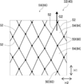
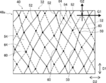
- FIG. 9 shows the crossing portion 48a, the first conductive layer 32 has the configuration shown in FIG. 4, and the second conductive layer 40 has the configuration shown in FIG.
- the orientation G1 of the direction component in which the vertices of the mesh cell in FIG. 4 are aligned in a straight line is orthogonal to the orientation G2 of the direction component in which the vertices of the mesh cell in FIG.
- the black circles shown in FIG. 9 indicate the apex 50 of the first mesh cell 54 and the apex 60 of the second mesh cell 64.
- the apex 60 of the second mesh cell 64 By arranging the apex 60 of the second mesh cell 64 in the first mesh cell 54, the apex 50 of the first mesh cell 54 and the apex 60 of the second mesh cell 64 become more difficult to be visually recognized, and the visibility is improved. Is improved, and the detection sensitivity of the touch panel 10 is increased.
- the dummy electrode is constituted by a mesh cell formed by the fine metal wires 52 formed in the first conductive layer 32 like the first electrode 34, and is electrically connected to the first electrode 34 adjacent in the second direction D2. Not connected.
- the dummy electrode is an electrode that is electrically floated and does not function as a detection electrode.
- the mesh pattern of the dummy electrode formed on the first conductive layer 32 is configured by the first mesh cell 54 in the same manner as the first electrode 34.
- the first electrode 34 and the dummy electrode can be formed by patterning a plurality of thin metal wires 52 formed on the entire surface 30 a of the transparent insulating substrate 30 in a mesh shape.
- dummy electrodes are disposed on the second conductive layer 40 also between the interelectrodes 42a of the plurality of second electrodes 42, similarly to the dummy electrodes disposed respectively between the interelectrodes 34a of the plurality of first electrodes 34. can do.
- the gaps between the plurality of second electrodes 42 between the electrodes 42a become inconspicuous, and the visibility of the touch panel 10 is improved.
- FIG. 10 is a flowchart showing how to obtain the direction component in which the apexes of the mesh cells of the conductive member for a touch panel according to the embodiment of the present invention are arranged in a straight line.
- FIG. 11 is a mesh cell of the conductive member for a touch panel according to the embodiment
- FIG. 12 is a schematic view showing an example of how to obtain a direction component in which vertices are aligned in a straight line
- FIG. 12 is another example of how to determine a direction component in which vertices of mesh cells of a conductive member for a touch panel according to an embodiment of the present invention are aligned.
- FIG. 10 is a flowchart showing how to obtain the direction component in which the apexes of the mesh cells of the conductive member for a touch panel according to the embodiment of the present invention are arranged in a straight line.
- FIG. 11 is a mesh cell of the conductive member for a touch panel according to the embodiment
- FIG. 12 is a schematic
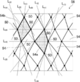
- FIG. 11 shows the first conductive layer 32, which has the same configuration as the first conductive layer 32 shown in FIG. 4 described above.
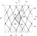
- FIG. 12 shows the first conductive layer 32, which has the same configuration as the first conductive layer 32 shown in FIG. 5 described above.
- the black circles shown in FIGS. 11 and 12 indicate the apexes 50 of the first mesh cell 54.
- the first conductive layer 32 illustrated in FIGS. 11 and 12, for example, images the first conductive layer 32 using an optical microscope to obtain a captured image. The captured image is taken into a personal computer, and the captured image is binarized to extract thin metal wires 52.
- the point of intersection of at least two metal thin wires 52 is taken as the point of intersection, and the point of intersection is extracted, and this point of intersection is made the apex 50 of the first mesh cell 54. Coordinates are set at each vertex 50. Thereby, the coordinates of the apex 50 in the first conductive layer 32 shown in FIGS. 11 and 12 can be identified. Note that the method of determining the direction component in which the vertexes of mesh cells are aligned in a straight line, which will be described below, is executed using various software in the personal computer using, for example, a personal computer.
- the direction component in which the vertices of the mesh cell are aligned in a straight line is represented by the arrangement of the vertices.
- the direction component in which the vertexes of the mesh cells are aligned in a straight line is obtained, for example, using the above-described captured image.
- the first mesh cell 54a and the first mesh cell 54b will be described as an example.
- the coordinates of the vertex 50 of the first mesh cell 54a and the coordinates of the vertex 50 of the first mesh cell 54b are specified in advance.
- a line segment connecting vertices in the mesh cell is obtained (step S10). Specifically, a line segment passing through the apex of the mesh cell of interest in the captured image is obtained. A line segment can be obtained as a line passing through two vertices. As shown in FIG. 11, line segments L 11 , L 12 , L 13 , L 14 , L 15 and L 16 connecting the apexes 50 of the first mesh cell 54 a are obtained. For even first mesh cell 54b, to obtain a line segment L 21, L 22, L 23 , L 24, L 25, L 26 connecting the vertices 50.
- N is the number of N-gons and represents the number of sides.
- NN3 The number of line segments of the second mesh cell (not shown) is the same as the number of line segments of the first mesh cell.
- step S 12 A line segment passing four or more mesh cells is detected from L 25 and L 26 (step S 12). Passing four or more vertices of a mesh cell is not limited as long as it passes through four or more vertices of four or more consecutive mesh cells in one direction.
- the four or more continuous mesh cells represent four or more adjacent mesh cells.
- the number of line segments to be detected passing through the mesh cells may be at least four as described above, and the number passing through the mesh cells is set in advance. The number passing through the mesh cell is, for example, four.
- the line segment L 26 is a line passing through four or more first mesh cells.
- the threshold value which a line segment and the vertex 50 agree in advance is set that the line segment passes four or more first mesh cells, and the distance between the line segment and the vertex 50 is within the above-mentioned threshold value. In the case of (1), the first mesh cell is passed.
- step S12 when a line segment passing four or more is detected, a parallel line segment is searched among the detected line segments (step S14).
- a change in distance is determined along the length direction of the target line segment.
- a set value parallel to the change in distance is determined in advance. If the change in distance is within the set value, it is assumed that the two line segments are parallel.
- the number of pairs of parallel line segments is determined.
- the number of sets of parallel line segments is the number of direction components in which the vertexes of the mesh cells are aligned in a straight line (step S16).
- the direction of the parallel line segment is the direction of the direction component in which the vertexes of the mesh cells are aligned in a straight line.
- step S12 the direction component in which the mesh cell vertices align in a straight line becomes zero.
- step S20 the direction component in which the apexes of the mesh cells are aligned in a straight line.
- line segments L 31 , L 32 , L 33 , L 34 , L 35 , and L 36 passing through the vertex 50 all pass through four or more first mesh cells. It is not a line segment. As described above, even when there are no line segments passing through four or more first mesh cells, the direction component in which the apexes of the mesh cells are aligned in a straight line is zero.
- the line segment In the direction component in which the apexes of mesh cells are arranged in a straight line, it is a line segment passing four or more mesh cells, but the upper limit thereof is a line segment passing ten mesh cells. It is the whole range. That is, it is preferable that the line segment cross the plurality of first electrodes 34. Furthermore, when a dummy electrode is provided adjacent to the first electrode 34, it is more preferable as a line segment to be a line segment passing through the plurality of first electrodes 34 and the dummy electrode.
- the direction component in which the apexes of the mesh cells are arranged in a straight line has been described by taking the first conductive layer 32 as an example, but the direction in which the apexes of the mesh cells are arranged in a straight line similarly to the first conductive layer 32 in the second conductive layer 40 The component can be determined.
- the fine metal wires 52 constitute the first mesh cell 54 and the second mesh cell 64.
- the line width of the thin metal wire 52 is 30 ⁇ m or less, preferably 0.5 ⁇ m to 10 ⁇ m, more preferably 1 ⁇ m to 5 ⁇ m, and most preferably 1 ⁇ m to 3 ⁇ m. If it is the above-mentioned range, the low resistance electrode excellent in visibility can be formed.
- the line width of the metal thin wire is preferably 10 ⁇ m to 50 ⁇ m, more preferably 30 ⁇ m or less, and still more preferably 15 ⁇ m or less. Within the above range, the area of the peripheral wiring portion of the touch panel can be reduced, that is, the frame can be narrowed.
- the thickness of the fine metal wire 52 is not particularly limited, but is preferably 10 ⁇ m or less, more preferably 1 ⁇ m or less, particularly preferably 0.01 to 1 ⁇ m, and preferably 0.05 to 0.8 ⁇ m. Most preferably. If it is the above-mentioned range, an electrode excellent in durability can be formed with a low resistance electrode.
- a cross-sectional image of the thin metal wire 52 is acquired using a scanning electron microscope. Next, the line width and thickness of the thin metal wire 52 are determined from the cross-sectional image.
- the first mesh cell 54 constituted by the thin metal wire 52 is exemplified by those shown in FIGS. 4 to 8 described above.
- the closed shape of the first mesh cell 54 is as described above.
- the first mesh cell 54 is an N-gon satisfying N ⁇ 3, and may be a triangle, a tetragon, a pentagon, a hexagon, an octagon, or the like, or a combination thereof. Further, the closed shape is not limited to one having a vertex connected by a straight line like an N-gon, and the vertex may be connected by a curve other than a straight line.
- the length of one side of the first mesh cell is preferably 50 ⁇ m to 1500 ⁇ m, more preferably 150 ⁇ m to 800 ⁇ m, and still more preferably 200 ⁇ m to 600 ⁇ m from the viewpoint of visibility.
- the aperture ratio of the mesh cell is preferably 90% or more, and more preferably 95% or more.
- the aperture ratio of the mesh cell corresponds to the unoccupied rate of the thin metal wire 52 in the region where the mesh cell is formed.
- the pattern formed by the first mesh cells is not limited to a regular pattern, but may be an irregular pattern.
- a plurality of mesh cells included in the pattern have a polygonal shape having an irregular side length of -10% to + 10% with respect to the average value of the side lengths of the respective cells.
- it can be a square shaped cell.
- moire can be suppressed, color noise can be reduced, and visibility can be improved.
- the second mesh cell can also have the same configuration as that of the first mesh cell.
- the metal contained in the metal thin wire 52 examples include metals or alloys such as gold (Au), silver (Ag), copper (Cu), and aluminum (Al). Among them, silver and copper are preferable because the conductivity of the fine metal wire is excellent.
- the fine metal wires 52 may be made of fine metal particles and a binder.
- the binder specifically, gelatin, (meth) acrylic resin, styrene resin, vinyl resin, polyolefin resin, polyester resin, polyurethane resin, polyamide resin, polycarbonate resin, polydiene resin, Examples thereof include at least one resin selected from the group consisting of epoxy resins, silicone resins, cellulose polymers and chitosan polymers, and copolymers made of monomers constituting these resins.
- the metal fine particles fine particles of silver, copper, gold or the like are used.
- the fine metal wires are not limited to those constituted of the above-mentioned metals or alloys, and, for example, metal oxides such as metal oxide particles, silver paste and copper paste, and metal pastes such as silver nanowires and copper nanowires It may contain nanowire particles.
- the fine metal wire may have a single layer structure or a multilayer structure.
- the metal fine wire for example, a structure in which a copper oxynitride layer, a copper layer and a copper oxynitride layer are sequentially laminated, or a structure in which molybdenum (Mo), aluminum (Al) and molybdenum (Mo) are sequentially laminated, Alternatively, a structure in which molybdenum (Mo), copper (Cu), and molybdenum (Mo) are sequentially stacked can be employed.
- the surface of the fine metal wire may be blackened by sulfidation or oxidation treatment. Furthermore, the structure which provides the blackening layer which makes a metal thin wire
- the blackening layer is, for example, for reducing the reflectance of the fine metal wire.
- the blackening layer can be composed of copper nitride, copper oxide, copper oxynitride, molybdenum oxide, AgO, Pd, carbon or another nitride or oxide, or the like.
- the blackening layer is disposed on the side where the thin metal wire is viewed, that is, the touch surface side.
- the method of manufacturing the metal fine wire 52 constituting the first conductive layer 32 and the second conductive layer 40 is not particularly limited as long as it can be formed on a transparent insulating substrate or the like, and it is not limited to JP 2014-159620 A.
- the plating method described in JP 2012-144761 A, etc., JP 2012-6377 A, JP 2014-112512 A, JP 2014-209332 A, JP 2015-22397 A, JP A 2016-192200 The silver salt method described in JP Gazette and WO 2016/157585 etc., the vapor deposition method described in JP 2014-29614 A etc., and the printing method using a conductive ink described in JP 2011-28985 A etc. Appropriately available.
- the line width (line) of the first peripheral wiring 37 and the second peripheral wiring 45 formed in the first peripheral wiring portion 38 and the second peripheral wiring portion 46 is preferably 50 ⁇ m or less, more preferably 30 ⁇ m or less, 15 micrometers or less are especially preferable.
- the space (space) between the first peripheral wiring 37 and the second peripheral wiring 45 is preferably 50 ⁇ m or less, more preferably 30 ⁇ m or less, and particularly preferably 15 ⁇ m or less. If the line width and the space are in the above-mentioned range, the regions of the first peripheral wiring portion 38 and the second peripheral wiring portion 46 can be narrowed, which is preferable.
- the first peripheral wiring 37 and the second peripheral wiring 45 can also be formed by the method of manufacturing the metal fine wire 52 described above, and the first peripheral wiring 37 and the first conductive layer 32 are the same material and the same. It can be formed simultaneously in the process.
- the second peripheral wiring 45 and the second conductive layer 40 can be simultaneously formed of the same material and in the same process.
- the transparent insulating substrate 30 supports the first conductive layer 32 or the second conductive layer 40.
- the type of the transparent insulating substrate 30 is not particularly limited as long as the above can be achieved.
- Examples of the material of the transparent insulating substrate 30 include transparent resin materials and transparent inorganic materials.
- the transparent resin material include acetyl cellulose-based resins such as triacetyl cellulose, polyester-based resins such as polyethylene terephthalate (PET) and polyethylene naphthalate (PEN), polyethylene (PE), polymethylpentene, Olefin resin such as cycloolefin polymer (COP), cycloolefin copolymer (COC), acrylic resin such as polymethyl methacrylate, polyurethane resin, polyether sulfone, polycarbonate, polysulfone, polyether, polyether ketone, acronitrile And methacrylonitrile and the like.
- the preferred thickness of the transparent resin material is 20 to 200 ⁇ m.
- the transparent inorganic material include, for example, alkali-free glass, alkali glass, chemically strengthened glass, soda glass, potash glass, glass such as lead glass, translucent piezoelectric ceramics (PLZT (lanthanum lead zirconate titanate) And the like, ceramics, quartz, fluorite and sapphire.
- the preferred thickness of the transparent inorganic material is 0.1 to 1.3 mm.
- the total light transmittance of the transparent insulating substrate 30 is preferably 40% to 100%. The total light transmittance is measured, for example, using “a method of determining the total light transmittance and the total light reflectance of plastic” defined in JIS K 7375: 2008.
- the transparent insulating substrate is not limited to an independent one as a member like the above-mentioned substrate, and may be in a form called a layer or a film. Therefore, the transparent insulating substrate may be a transparent insulating layer or a transparent insulating film coated with an acrylic resin.
- One of the preferred embodiments of the transparent insulating substrate 30 is a treated substrate that has been subjected to at least one treatment selected from the group consisting of atmospheric pressure plasma treatment, corona discharge treatment, and ultraviolet radiation treatment.
- a hydrophilic group such as an OH group is introduced on the surface on which the first conductive layer 32 and the second conductive layer 40 are provided, and the first conductive layer 32 is formed.
- the adhesion with the second conductive layer 40 is improved.
- atmospheric pressure plasma treatment is preferable in that adhesion with the first conductive layer 32 and the second conductive layer 40 is further improved.
- the transparent insulating substrate 30 it is preferable to have an underlayer containing a polymer on the surface on which the first conductive layer 32 and the second conductive layer 40 are provided.
- the adhesion between the first conductive layer 32 and the second conductive layer 40 and the transparent insulating substrate 30 is further improved.
- the formation method of a base layer is not specifically limited,
- macromolecule is apply
- the composition for base layer formation may contain a solvent, if necessary.
- the type of solvent is not particularly limited.
- an acrylic styrene latex containing fine particles of gelatin, acrylic resin, urethane resin, or inorganic or polymer may be used as a composition for forming an underlayer containing a polymer.
- the thickness of the base layer is not particularly limited, but is preferably 0.02 to 2.0 ⁇ m in that the adhesion between the first conductive layer 32 and the second conductive layer 40 and the transparent insulating substrate 30 is more excellent. 0.03 to 1.5 ⁇ m is more preferable.
- an ultraviolet absorbing layer may be provided as another layer between the transparent insulating substrate 30 and the first conductive layer 32 and the second conductive layer 40 as necessary. Moreover, you may form the following functional films as needed.
- a transparent protective layer may be formed on the fine metal wire 52.
- organic films such as gelatin, acrylic resin, urethane resin, acrylic styrene latex and the like, and inorganic films such as silicon dioxide can be used, and the film thickness is preferably 10 nm or more and 10000 nm or less .
- the transparent coat layer is made of an organic film such as an acrylic resin or a urethane resin, and is formed in the sensing area 48, and has a thickness of 1 ⁇ m to 100 ⁇ m.
- a peripheral wiring insulating film may be formed on the first peripheral wiring 37 and the second peripheral wiring 45 shown in FIG. 2 for the purpose of preventing migration of the peripheral wiring and corrosion of the peripheral wiring.
- the peripheral wiring insulating film an organic film such as an acrylic resin or a urethane resin is used, and the film thickness is preferably 1 ⁇ m to 30 ⁇ m.
- the peripheral wiring insulating film may be formed on only one of the first peripheral wiring 37 and the second peripheral wiring 45.
- the present invention is basically configured as described above. As mentioned above, although the conductive member for touch panels and touch panel of the present invention were explained in detail, the present invention is not limited to the above-mentioned embodiment, and various improvement or change may be made in the range which does not deviate from the main point of the present invention Of course.
- a conductive member for a touch panel is disposed on a display device (LCD (Liquid Crystal Display)), and the conductive member for a touch panel is observed under a fluorescent lamp from the side on which a molybdenum oxide layer of a glass substrate described later is formed.
- LCD Liquid Crystal Display
- a two-stage evaluation of "Moiré can not be recognized” was performed. “A”: very good level where 18 or more of 20 observers judged “no moiré recognition” “B”: 12 or more out of 20 observers 17 or less say “moiré can not be recognized” Judgment level with no problem in practical use “C”: Less than 11 people judged that "moire can not be recognized” among 20 observers
- a glass substrate having a thickness of 0.7 mm is prepared.
- a molybdenum oxide layer (blackened layer) having a thickness of 30 nm was formed on the first surface of the glass substrate by sputtering.
- a lower molybdenum layer having a thickness of 30 nm was formed on the molybdenum oxide layer by sputtering.
- a copper layer having a thickness of 300 nm was formed on the lower molybdenum layer by sputtering.
- an upper molybdenum layer having a thickness of 50 nm is formed on the copper layer by sputtering, and a first conductive film composed of a molybdenum oxide layer, a lower molybdenum layer, a copper layer, and an upper molybdenum layer is formed.
- a resist film was formed by coating on the first conductive film, and the resist film was pattern-exposed through an exposure mask and developed to form a resist pattern.
- FIG. 13 is formed of a rhombic mesh cell having an acute angle of 60 ° and a side length of 350 ⁇ m.
- the mesh patterns of FIGS. 4 to 7 and 11 are mesh patterns formed by moving the mesh intersection points of FIG. 13 within a distance of 10% (35 ⁇ m) of one side of the mesh cell.
- the line width of the thin metal wire was 3 ⁇ m.
- Example 1 In Example 1, the line width of the thin metal wire was 3 ⁇ m.
- the mesh pattern is shown in FIG. In the first embodiment, the direction component in which the apexes of mesh cells are aligned in a straight line is one.
- the intersection weight index (area of intersection of mesh / square of line width of metal thin wire forming mesh) was 2.5.
- the intersection weight index (area of mesh intersection point / square of line width of metal thin wire forming mesh) was measured as follows. The intersection weight index is an average of five mesh intersection points.
- the line width of the thin metal wire was measured at the midpoint between mesh intersection points (mid point of the side of the mesh cell).
- the line width of the thin metal wire is an average value of the line widths of lines extending from mesh intersections.
- the mesh shape of the mesh pattern shown in FIG. 4 since it is a quadrilateral, it is an average value of the line widths of the four thin metal wires extending from the intersection.
- the intersection point thickness index of Examples 2 to 4 and Comparative Examples 1 and 2 shown below was also measured in the same manner as Example 1.
- Example 2 The second embodiment is the same as the first embodiment except that the mesh pattern shown in FIG. 5 is the pattern shown in FIG. 5 and the direction components of the mesh cell are aligned in a straight line are zero as compared with the first embodiment. It is the same. In addition, the intersection weight index (area of intersection of mesh / square of line width of metal thin wire forming mesh) was 2.5.
- Example 3 The third embodiment is the same as the first embodiment in the configuration and the manufacturing method as the first embodiment except that the mesh pattern is a pattern shown in FIG. In addition, the intersection weight index (area of intersection of mesh / square of line width of metal thin wire forming mesh) was 2.5.
- the fourth embodiment is the same as the first embodiment in the configuration and the manufacturing method as the first embodiment except that the mesh pattern is a pattern shown in FIG. 7 and the shape of the mesh cell is triangular.
- the intersection weight index (area of intersection of mesh / square of line width of metal thin wire forming mesh) was 2.9.
- Comparative Example 1 is the same as Example 1 except that the mesh pattern is a pattern shown in FIG. 13 as compared with Example 1, and the direction component of the mesh cell vertex is aligned in a straight line is four. It is the same. In addition, the intersection weight index (area of intersection of mesh / square of line width of metal thin wire forming mesh) was 2.4.
- Comparative Example 2 is the same as Example 1 except that the mesh pattern is the pattern shown in FIG. 14 as compared with Example 1, and the direction component of the mesh cell vertex is aligned in a straight line is 2. It is the same. In the mesh pattern of FIG. 14, the thin metal wires of the diamond-shaped regular mesh pattern of FIG.
- the side length of the mesh cell is 90% to 110% of the side length of the mesh cell of FIG.
- the mesh pattern is deformed so as to be random.
- the intersection weight index (area of intersection of mesh / square of line width of metal thin wire forming mesh) was 2.3.
- Examples 1 to 4 were superior to Comparative Examples 1 and 2 in the evaluation of the intersection appearance.
- the evaluation of noise was better when the direction component in which the vertexes of the mesh cells are aligned in a straight line is 1.
- the evaluation of the moiré was better in the case of a quadrangle.
- touch panels of Examples 10 to 13 and Comparative Examples 10 and 11 shown below were manufactured. With respect to the touch panels of Example 10 to Example 13 and Comparative Example 10 and Comparative Example 11, the intersection appearance was observed, and the noise, the moire, and the touch sensitivity were evaluated. The results are shown in Table 2 below. The evaluation of noise and moiré is not the conductive member for the touch panel but the touch panel, and the observation is performed under a fluorescent lamp from the side of the glass substrate on which the molybdenum oxide layer is formed. Since the same, the detailed description is omitted. The touch sensitivity will be described below.
- a glass substrate having a thickness of 0.7 mm is prepared.
- a molybdenum oxide layer (blackened layer) having a thickness of 30 nm was formed on the first surface of the glass substrate by sputtering, and then a thickness of 30 nm was formed on the molybdenum oxide layer by sputtering.
- the lower molybdenum layer was formed.
- a copper layer having a thickness of 300 nm was formed on the lower molybdenum layer by sputtering.
- an upper molybdenum layer having a thickness of 50 nm is formed on the copper layer by sputtering, and a first conductive film composed of a molybdenum oxide layer, a lower molybdenum layer, a copper layer, and an upper molybdenum layer is formed.
- a resist film was formed by coating on the first conductive film, and the resist film was pattern-exposed through an exposure mask and developed to form a resist pattern.
- an interlayer insulating film made of acrylic resin and having a thickness of 10 ⁇ m was formed on the first conductive layer.
- a second conductive film formed of a molybdenum oxide layer, a lower molybdenum layer, a copper layer, and an upper molybdenum layer was formed on the interlayer insulating film by sputtering.
- the second conductive layer was formed by performing the steps of resist application, pattern exposure, development, etching, and resist peeling in the same manner as the first conductive film.
- a protective layer made of acrylic resin was formed on the second conductive layer to form a touch panel.
- the touch panel has a configuration in which the second conductive layer is disposed on the uppermost layer on the molybdenum oxide side of the glass substrate.
- the touch sensitivity was evaluated as follows. Using the probe robot in order at positions of 10,000 points set in advance on the surface of the touch panel, each touch position was detected while contacting a stylus pen with a tip diameter of 2 mm. And the detection result of 10,000 places and the setting value corresponding to it were compared. The sensitivity was evaluated according to the following evaluation criteria using the 9973th value counted from the smallest absolute value of the difference vector between the detection position and the setting position. "A”: the 9973th value mentioned above is less than 1.0 mm "B”: the 9973th value mentioned above is less than 1.0m and 2.0mm "C”: the 9973th value mentioned above is 2.0 mm or more
- Example 10 the first mesh pattern of the first conductive layer is a pattern shown in FIG. 4, and the second mesh pattern of the second conductive layer is a pattern shown in FIG.
- the first conductive layer and the second conductive layer were overlapped such that the apex of the first mesh cell was disposed in the second mesh cell as shown in FIG.
- the first conductive layer has a direction component in which the vertices of mesh cells are aligned in a straight line
- the second conductive layer has a direction component in which the vertices of mesh cells are aligned in a straight line
- the vertices of mesh cells are straight.
- the direction components aligned in are orthogonal to each other.
- the cross point thickness index of the first conductive layer and the second conductive layer was 2.5, respectively.
- the intersection weight index was measured in the same manner as in Example 1 of the first example described above.
- the intersection point thickness index of Examples 11 to 13 and Comparative Examples 10 and 11 shown below was also measured in the same manner as in Example 1 of the first example described above.
- Example 11 is different from Example 10 in that the first mesh pattern of the first conductive layer is the pattern shown in FIG. 5 and the second mesh pattern of the second conductive layer is the pattern shown in FIG.
- the configuration and the manufacturing method are the same as in Example 1.
- the direction component in which the apexes of mesh cells are aligned in a straight line is zero.
- the first conductive layer and the second conductive layer were a combination of the same mesh pattern.
- the cross point thickness index of the first conductive layer and the second conductive layer was 2.5, respectively.
- Example 12 is different from Example 10 in that the first mesh pattern of the first conductive layer is the pattern shown in FIG.
- Example 4 and the second mesh pattern of the second conductive layer is the pattern shown in FIG.
- the configuration and the manufacturing method are the same as in Example 1.
- Example 12 the first conductive layer and the second conductive layer in Example 1 are the same mesh pattern combination.
- the direction components in which the vertexes of the mesh cells are aligned in a straight line do not intersect.
- the cross point thickness index of the first conductive layer and the second conductive layer was 2.5, respectively.
- Example 13 is different from Example 10 in that the first mesh pattern of the first conductive layer is the pattern shown in FIG. 7 and the second mesh pattern of the second conductive layer is the pattern shown in FIG.
- the configuration and the manufacturing method are the same as in Example 1.
- the mesh cells of the first conductive layer and the second conductive layer are triangular in shape, and the direction component of the mesh cell apex is aligned in a straight line is 1, and the mesh cell apex is a straight line.
- the direction components in line are orthogonal.
- the mesh pattern of FIG. 8 is a mesh pattern formed by moving the intersection points of the mesh of FIG. 13 within a distance of 10% (35 ⁇ m) of the length of one side of the mesh cell, and the line width of the metal thin wire is 3 ⁇ m.
- the cross point index of the first conductive layer and the second conductive layer was 2.9, respectively.
- Comparative Example 10 is different from Example 10 in that the first mesh pattern of the first conductive layer is a pattern shown in FIG. 13 and the second mesh pattern of the second conductive layer is a pattern shown in FIG.
- the construction and the production method are the same as in Example 10.
- the mesh cells of the first conductive layer and the second conductive layer have a rhombus shape, and the direction component in which the apexes of the mesh cells are aligned in a straight line is 4 in all cases.
- the cross point index of the first conductive layer and the second conductive layer was 2.4, respectively.
- Comparative example 11 Comparative Example 11 is different from Example 10 in that the first mesh pattern of the first conductive layer is a pattern shown in FIG.
- Example 14 and the second mesh pattern of the second conductive layer is a pattern shown in FIG.
- the construction and the production method are the same as in Example 10.
- the first conductive layer and the second conductive layer both have a direction component in which the apexes of mesh cells are aligned in a straight line.
- the cross point thickness index of each of the first conductive layer and the second conductive layer was 2.3.
- Examples 10 to 13 were superior in evaluation of intersection appearance as compared with Comparative Example 10 and Comparative Example 11.
- the evaluation of noise and the evaluation of touch sensitivity are better when the direction component in which the vertexes of the mesh cell are aligned is 1 is 1.
- the shape of the mesh cell was better in the evaluation of noise, the evaluation of moiré and the evaluation of touch sensitivity in the case of the quadrangle.
- Example 12 although the direction component in which the apexes of the mesh cells are aligned in a straight line is 1 for both the first conductive layer and the second conductive layer, the direction component in which the apexes of the mesh cells in the first conductive layer are aligned in a straight line
- the vertexes of the mesh cells in the two conductive layers do not intersect with the direction component in which the vertexes of the mesh cells in the second conductive layer intersect, but in Example 10, the mesh cell in the vertex of the first conductive layer aligns in a straight line and the mesh cell of the second conductive layer
- the evaluation of the appearance of the intersection point was excellent because the direction component of the apex of the line in a straight line intersects at right angles.
Landscapes
- Engineering & Computer Science (AREA)
- General Engineering & Computer Science (AREA)
- Theoretical Computer Science (AREA)
- Human Computer Interaction (AREA)
- Physics & Mathematics (AREA)
- General Physics & Mathematics (AREA)
- Quality & Reliability (AREA)
- Position Input By Displaying (AREA)
Abstract
L'invention concerne un élément conducteur de panneau tactile qui présente une excellente visibilité, et un panneau tactile. L'élément conducteur de panneau tactile comporte un substrat isolant transparent et une première couche conductrice formée sur le substrat isolant transparent. La première couche conductrice de l'élément conducteur de panneau tactile a un premier motif de maillage configuré à partir d'une pluralité de premières cellules de maillage fermées obtenues par connexion d'une pluralité de pics avec un fil métallique mince. Il n'y a pas plus d'une direction dans laquelle les pics de la pluralité de premières cellules maillées sont agencés en ligne droite. Le panneau tactile comprend ledit élément conducteur de panneau tactile.
Priority Applications (2)
| Application Number | Priority Date | Filing Date | Title |
|---|---|---|---|
| JP2019532501A JP6977042B2 (ja) | 2017-07-27 | 2018-07-12 | タッチパネル用導電部材およびタッチパネル |
| US16/715,138 US11079887B2 (en) | 2017-07-27 | 2019-12-16 | Conductive member for touch panel and touch panel |
Applications Claiming Priority (2)
| Application Number | Priority Date | Filing Date | Title |
|---|---|---|---|
| JP2017145155 | 2017-07-27 | ||
| JP2017-145155 | 2017-07-27 |
Related Child Applications (1)
| Application Number | Title | Priority Date | Filing Date |
|---|---|---|---|
| US16/715,138 Continuation US11079887B2 (en) | 2017-07-27 | 2019-12-16 | Conductive member for touch panel and touch panel |
Publications (1)
| Publication Number | Publication Date |
|---|---|
| WO2019021835A1 true WO2019021835A1 (fr) | 2019-01-31 |
Family
ID=65040648
Family Applications (1)
| Application Number | Title | Priority Date | Filing Date |
|---|---|---|---|
| PCT/JP2018/026257 Ceased WO2019021835A1 (fr) | 2017-07-27 | 2018-07-12 | Élément conducteur de panneau tactile et panneau tactile |
Country Status (3)
| Country | Link |
|---|---|
| US (1) | US11079887B2 (fr) |
| JP (1) | JP6977042B2 (fr) |
| WO (1) | WO2019021835A1 (fr) |
Cited By (1)
| Publication number | Priority date | Publication date | Assignee | Title |
|---|---|---|---|---|
| WO2025161248A1 (fr) * | 2024-01-29 | 2025-08-07 | 武汉华星光电半导体显示技术有限公司 | Écran d'affichage et dispositif d'affichage |
Families Citing this family (6)
| Publication number | Priority date | Publication date | Assignee | Title |
|---|---|---|---|---|
| WO2019093049A1 (fr) * | 2017-11-13 | 2019-05-16 | 富士フイルム株式会社 | Élément électroconducteur et panneau tactile |
| JP7062609B2 (ja) * | 2018-03-27 | 2022-05-06 | 富士フイルム株式会社 | 導電性部材、導電性フィルム、これを備える表示装置、タッチパネル、導電性部材の配線パターンの作製方法、及び導電性フィルムの配線パターンの作製方法 |
| WO2019189201A1 (fr) * | 2018-03-27 | 2019-10-03 | 富士フイルム株式会社 | Élément conducteur, film conducteur, dispositif d'affichage et panneau tactile |
| WO2020108316A1 (fr) * | 2018-11-28 | 2020-06-04 | 无锡变格新材料科技有限公司 | Panneau tactile et dispositif d'affichage tactile |
| JP7266955B2 (ja) * | 2021-05-20 | 2023-05-01 | Nissha株式会社 | 導電シート、タッチセンサ及びタッチセンサの製造方法 |
| TWI836888B (zh) * | 2023-02-02 | 2024-03-21 | 友達光電股份有限公司 | 觸控顯示裝置 |
Citations (1)
| Publication number | Priority date | Publication date | Assignee | Title |
|---|---|---|---|---|
| JP2014191657A (ja) * | 2013-03-27 | 2014-10-06 | Japan Display Inc | タッチ検出機能付き表示装置及び電子機器 |
Family Cites Families (16)
| Publication number | Priority date | Publication date | Assignee | Title |
|---|---|---|---|---|
| JPH11110115A (ja) * | 1997-09-30 | 1999-04-23 | Fujitsu General Ltd | デジタイザ装置 |
| US8599150B2 (en) * | 2009-10-29 | 2013-12-03 | Atmel Corporation | Touchscreen electrode configuration |
| JP2012163951A (ja) * | 2011-01-18 | 2012-08-30 | Fujifilm Corp | 導電性フイルムを備える表示装置及び導電性フイルム |
| US8797285B2 (en) * | 2011-04-18 | 2014-08-05 | Atmel Corporation | Panel |
| US20140216783A1 (en) | 2013-02-05 | 2014-08-07 | David P. Trauernicht | Micro-wire pattern with offset intersections |
| CN103218077B (zh) * | 2013-03-30 | 2016-04-13 | 南昌欧菲光显示技术有限公司 | 滤光片模块及包含该滤光片模块的触摸显示屏 |
| WO2015030090A1 (fr) * | 2013-08-30 | 2015-03-05 | 富士フイルム株式会社 | Film électroconducteur, écran tactile et dispositif d'affichage utilisant ce dernier, et procédé d'évaluation d'un film électroconducteur |
| JP6503728B2 (ja) | 2013-12-26 | 2019-04-24 | 大日本印刷株式会社 | 表示装置 |
| KR102500994B1 (ko) * | 2014-10-17 | 2023-02-16 | 가부시키가이샤 한도오따이 에네루기 켄큐쇼 | 터치 패널 |
| JP6610053B2 (ja) | 2015-07-24 | 2019-11-27 | 大日本印刷株式会社 | タッチパネルセンサ、タッチパネル装置および表示装置 |
| WO2017018051A1 (fr) * | 2015-07-24 | 2017-02-02 | 富士フイルム株式会社 | Procédé de conception de motif de maillage de film conducteur pour panneau tactile, procédé de fabrication de film conducteur pour panneau tactile, et film conducteur pour panneau tactile |
| JP6511382B2 (ja) | 2015-10-16 | 2019-05-15 | 富士フイルム株式会社 | 導電性フィルム、及びこれを備える表示装置 |
| JP6559552B2 (ja) * | 2015-11-18 | 2019-08-14 | 株式会社Vtsタッチセンサー | 導電性フィルム、タッチパネル、および、表示装置 |
| KR102415044B1 (ko) * | 2015-12-11 | 2022-07-01 | 삼성디스플레이 주식회사 | 터치 스크린 패널, 이의 제조 방법 및 터치 스크린 패널을 포함하는 터치 표시 장치 |
| WO2017126212A1 (fr) * | 2016-01-22 | 2017-07-27 | 富士フイルム株式会社 | Film électroconducteur et panneau tactile |
| KR102357521B1 (ko) * | 2017-06-02 | 2022-02-03 | 삼성디스플레이 주식회사 | 표시 장치 |
-
2018
- 2018-07-12 WO PCT/JP2018/026257 patent/WO2019021835A1/fr not_active Ceased
- 2018-07-12 JP JP2019532501A patent/JP6977042B2/ja active Active
-
2019
- 2019-12-16 US US16/715,138 patent/US11079887B2/en active Active
Patent Citations (1)
| Publication number | Priority date | Publication date | Assignee | Title |
|---|---|---|---|---|
| JP2014191657A (ja) * | 2013-03-27 | 2014-10-06 | Japan Display Inc | タッチ検出機能付き表示装置及び電子機器 |
Cited By (1)
| Publication number | Priority date | Publication date | Assignee | Title |
|---|---|---|---|---|
| WO2025161248A1 (fr) * | 2024-01-29 | 2025-08-07 | 武汉华星光电半导体显示技术有限公司 | Écran d'affichage et dispositif d'affichage |
Also Published As
| Publication number | Publication date |
|---|---|
| US11079887B2 (en) | 2021-08-03 |
| JP6977042B2 (ja) | 2021-12-08 |
| US20200117301A1 (en) | 2020-04-16 |
| JPWO2019021835A1 (ja) | 2020-07-09 |
Similar Documents
| Publication | Publication Date | Title |
|---|---|---|
| TWI746795B (zh) | 觸控面板及觸控面板用導電性片及觸控感測器 | |
| JP6977042B2 (ja) | タッチパネル用導電部材およびタッチパネル | |
| CN107111394B (zh) | 导电性薄膜及具备该导电性薄膜的触摸面板传感器 | |
| CN110998496B (zh) | 触摸面板用导电部件及触摸面板 | |
| US10852896B2 (en) | Touch panel used as touch sensor to increase touch detection sensitivity, including conductive member and conductive sheet | |
| US20110007011A1 (en) | Capacitive touch screen with a mesh electrode | |
| TW201520862A (zh) | 觸控面板 | |
| WO2018034119A1 (fr) | Film conducteur et panneau tactile | |
| CN107533392A (zh) | 触摸窗以及具有触摸窗的显示器 | |
| CN212675531U (zh) | 触摸面板用电极部件、触摸面板及图像显示装置 | |
| TWI696943B (zh) | 可降低寄生電容之觸控面板 | |
| US11132093B2 (en) | Touch sensor, touch panel, conductive member for touch panel, and conductive sheet for touch panel | |
| CN212675529U (zh) | 触摸面板用电极部件、触摸面板及图像显示装置 | |
| CN111694469A (zh) | 可降低寄生电容的触控面板 | |
| KR20160003533A (ko) | 터치 윈도우 | |
| KR20170001336A (ko) | 터치 윈도우 | |
| KR20160005595A (ko) | 터치 윈도우 | |
| KR20160090070A (ko) | 터치 윈도우 |
Legal Events
| Date | Code | Title | Description |
|---|---|---|---|
| 121 | Ep: the epo has been informed by wipo that ep was designated in this application |
Ref document number: 18839232 Country of ref document: EP Kind code of ref document: A1 |
|
| DPE1 | Request for preliminary examination filed after expiration of 19th month from priority date (pct application filed from 20040101) | ||
| ENP | Entry into the national phase |
Ref document number: 2019532501 Country of ref document: JP Kind code of ref document: A |
|
| NENP | Non-entry into the national phase |
Ref country code: DE |
|
| 122 | Ep: pct application non-entry in european phase |
Ref document number: 18839232 Country of ref document: EP Kind code of ref document: A1 |