WO2019031204A1 - ダイオード - Google Patents
ダイオード Download PDFInfo
- Publication number
- WO2019031204A1 WO2019031204A1 PCT/JP2018/027416 JP2018027416W WO2019031204A1 WO 2019031204 A1 WO2019031204 A1 WO 2019031204A1 JP 2018027416 W JP2018027416 W JP 2018027416W WO 2019031204 A1 WO2019031204 A1 WO 2019031204A1
- Authority
- WO
- WIPO (PCT)
- Prior art keywords
- type semiconductor
- semiconductor layer
- type
- diode
- junction
- Prior art date
- Legal status (The legal status is an assumption and is not a legal conclusion. Google has not performed a legal analysis and makes no representation as to the accuracy of the status listed.)
- Ceased
Links
Images





Classifications
-
- H—ELECTRICITY
- H10—SEMICONDUCTOR DEVICES; ELECTRIC SOLID-STATE DEVICES NOT OTHERWISE PROVIDED FOR
- H10D—INORGANIC ELECTRIC SEMICONDUCTOR DEVICES
- H10D62/00—Semiconductor bodies, or regions thereof, of devices having potential barriers
- H10D62/80—Semiconductor bodies, or regions thereof, of devices having potential barriers characterised by the materials
-
- C—CHEMISTRY; METALLURGY
- C30—CRYSTAL GROWTH
- C30B—SINGLE-CRYSTAL GROWTH; UNIDIRECTIONAL SOLIDIFICATION OF EUTECTIC MATERIAL OR UNIDIRECTIONAL DEMIXING OF EUTECTOID MATERIAL; REFINING BY ZONE-MELTING OF MATERIAL; PRODUCTION OF A HOMOGENEOUS POLYCRYSTALLINE MATERIAL WITH DEFINED STRUCTURE; SINGLE CRYSTALS OR HOMOGENEOUS POLYCRYSTALLINE MATERIAL WITH DEFINED STRUCTURE; AFTER-TREATMENT OF SINGLE CRYSTALS OR A HOMOGENEOUS POLYCRYSTALLINE MATERIAL WITH DEFINED STRUCTURE; APPARATUS THEREFOR
- C30B25/00—Single-crystal growth by chemical reaction of reactive gases, e.g. chemical vapour-deposition growth
-
- C—CHEMISTRY; METALLURGY
- C30—CRYSTAL GROWTH
- C30B—SINGLE-CRYSTAL GROWTH; UNIDIRECTIONAL SOLIDIFICATION OF EUTECTIC MATERIAL OR UNIDIRECTIONAL DEMIXING OF EUTECTOID MATERIAL; REFINING BY ZONE-MELTING OF MATERIAL; PRODUCTION OF A HOMOGENEOUS POLYCRYSTALLINE MATERIAL WITH DEFINED STRUCTURE; SINGLE CRYSTALS OR HOMOGENEOUS POLYCRYSTALLINE MATERIAL WITH DEFINED STRUCTURE; AFTER-TREATMENT OF SINGLE CRYSTALS OR A HOMOGENEOUS POLYCRYSTALLINE MATERIAL WITH DEFINED STRUCTURE; APPARATUS THEREFOR
- C30B29/00—Single crystals or homogeneous polycrystalline material with defined structure characterised by the material or by their shape
- C30B29/10—Inorganic compounds or compositions
- C30B29/16—Oxides
-
- H—ELECTRICITY
- H10—SEMICONDUCTOR DEVICES; ELECTRIC SOLID-STATE DEVICES NOT OTHERWISE PROVIDED FOR
- H10D—INORGANIC ELECTRIC SEMICONDUCTOR DEVICES
- H10D62/00—Semiconductor bodies, or regions thereof, of devices having potential barriers
- H10D62/10—Shapes, relative sizes or dispositions of the regions of the semiconductor bodies; Shapes of the semiconductor bodies
- H10D62/102—Constructional design considerations for preventing surface leakage or controlling electric field concentration
- H10D62/103—Constructional design considerations for preventing surface leakage or controlling electric field concentration for increasing or controlling the breakdown voltage of reverse-biased devices
- H10D62/105—Constructional design considerations for preventing surface leakage or controlling electric field concentration for increasing or controlling the breakdown voltage of reverse-biased devices by having particular doping profiles, shapes or arrangements of PN junctions; by having supplementary regions, e.g. junction termination extension [JTE]
- H10D62/106—Constructional design considerations for preventing surface leakage or controlling electric field concentration for increasing or controlling the breakdown voltage of reverse-biased devices by having particular doping profiles, shapes or arrangements of PN junctions; by having supplementary regions, e.g. junction termination extension [JTE] having supplementary regions doped oppositely to or in rectifying contact with regions of the semiconductor bodies, e.g. guard rings with PN or Schottky junctions
-
- H—ELECTRICITY
- H10—SEMICONDUCTOR DEVICES; ELECTRIC SOLID-STATE DEVICES NOT OTHERWISE PROVIDED FOR
- H10D—INORGANIC ELECTRIC SEMICONDUCTOR DEVICES
- H10D62/00—Semiconductor bodies, or regions thereof, of devices having potential barriers
- H10D62/40—Crystalline structures
- H10D62/402—Amorphous materials
-
- H—ELECTRICITY
- H10—SEMICONDUCTOR DEVICES; ELECTRIC SOLID-STATE DEVICES NOT OTHERWISE PROVIDED FOR
- H10D—INORGANIC ELECTRIC SEMICONDUCTOR DEVICES
- H10D62/00—Semiconductor bodies, or regions thereof, of devices having potential barriers
- H10D62/80—Semiconductor bodies, or regions thereof, of devices having potential barriers characterised by the materials
- H10D62/82—Heterojunctions
- H10D62/8271—Heterojunctions comprising only oxide semiconductor materials heterojunctions, e.g. IGZO/IZO
-
- H—ELECTRICITY
- H10—SEMICONDUCTOR DEVICES; ELECTRIC SOLID-STATE DEVICES NOT OTHERWISE PROVIDED FOR
- H10D—INORGANIC ELECTRIC SEMICONDUCTOR DEVICES
- H10D62/00—Semiconductor bodies, or regions thereof, of devices having potential barriers
- H10D62/80—Semiconductor bodies, or regions thereof, of devices having potential barriers characterised by the materials
- H10D62/875—Semiconductor bodies, or regions thereof, of devices having potential barriers characterised by the materials being semiconductor metal oxide, e.g. InGaZnO
-
- H—ELECTRICITY
- H10—SEMICONDUCTOR DEVICES; ELECTRIC SOLID-STATE DEVICES NOT OTHERWISE PROVIDED FOR
- H10D—INORGANIC ELECTRIC SEMICONDUCTOR DEVICES
- H10D64/00—Electrodes of devices having potential barriers
- H10D64/60—Electrodes characterised by their materials
- H10D64/62—Electrodes ohmically coupled to a semiconductor
-
- H—ELECTRICITY
- H10—SEMICONDUCTOR DEVICES; ELECTRIC SOLID-STATE DEVICES NOT OTHERWISE PROVIDED FOR
- H10D—INORGANIC ELECTRIC SEMICONDUCTOR DEVICES
- H10D64/00—Electrodes of devices having potential barriers
- H10D64/60—Electrodes characterised by their materials
- H10D64/64—Electrodes comprising a Schottky barrier to a semiconductor
-
- H—ELECTRICITY
- H10—SEMICONDUCTOR DEVICES; ELECTRIC SOLID-STATE DEVICES NOT OTHERWISE PROVIDED FOR
- H10D—INORGANIC ELECTRIC SEMICONDUCTOR DEVICES
- H10D8/00—Diodes
- H10D8/422—PN diodes having the PN junctions in mesas
-
- H—ELECTRICITY
- H10—SEMICONDUCTOR DEVICES; ELECTRIC SOLID-STATE DEVICES NOT OTHERWISE PROVIDED FOR
- H10D—INORGANIC ELECTRIC SEMICONDUCTOR DEVICES
- H10D8/00—Diodes
- H10D8/60—Schottky-barrier diodes
-
- H—ELECTRICITY
- H10—SEMICONDUCTOR DEVICES; ELECTRIC SOLID-STATE DEVICES NOT OTHERWISE PROVIDED FOR
- H10D—INORGANIC ELECTRIC SEMICONDUCTOR DEVICES
- H10D99/00—Subject matter not provided for in other groups of this subclass
-
- H—ELECTRICITY
- H10—SEMICONDUCTOR DEVICES; ELECTRIC SOLID-STATE DEVICES NOT OTHERWISE PROVIDED FOR
- H10D—INORGANIC ELECTRIC SEMICONDUCTOR DEVICES
- H10D64/00—Electrodes of devices having potential barriers
- H10D64/01—Manufacture or treatment
- H10D64/011—Manufacture or treatment of electrodes ohmically coupled to a semiconductor
-
- H—ELECTRICITY
- H10—SEMICONDUCTOR DEVICES; ELECTRIC SOLID-STATE DEVICES NOT OTHERWISE PROVIDED FOR
- H10P—GENERIC PROCESSES OR APPARATUS FOR THE MANUFACTURE OR TREATMENT OF DEVICES COVERED BY CLASS H10
- H10P14/00—Formation of materials, e.g. in the shape of layers or pillars
- H10P14/20—Formation of materials, e.g. in the shape of layers or pillars of semiconductor materials
- H10P14/22—Formation of materials, e.g. in the shape of layers or pillars of semiconductor materials using physical deposition, e.g. vacuum deposition or sputtering
-
- H—ELECTRICITY
- H10—SEMICONDUCTOR DEVICES; ELECTRIC SOLID-STATE DEVICES NOT OTHERWISE PROVIDED FOR
- H10P—GENERIC PROCESSES OR APPARATUS FOR THE MANUFACTURE OR TREATMENT OF DEVICES COVERED BY CLASS H10
- H10P14/00—Formation of materials, e.g. in the shape of layers or pillars
- H10P14/20—Formation of materials, e.g. in the shape of layers or pillars of semiconductor materials
- H10P14/29—Formation of materials, e.g. in the shape of layers or pillars of semiconductor materials characterised by the substrates
- H10P14/2901—Materials
- H10P14/2918—Materials being semiconductor metal oxides
-
- H—ELECTRICITY
- H10—SEMICONDUCTOR DEVICES; ELECTRIC SOLID-STATE DEVICES NOT OTHERWISE PROVIDED FOR
- H10P—GENERIC PROCESSES OR APPARATUS FOR THE MANUFACTURE OR TREATMENT OF DEVICES COVERED BY CLASS H10
- H10P14/00—Formation of materials, e.g. in the shape of layers or pillars
- H10P14/20—Formation of materials, e.g. in the shape of layers or pillars of semiconductor materials
- H10P14/29—Formation of materials, e.g. in the shape of layers or pillars of semiconductor materials characterised by the substrates
- H10P14/2924—Structures
- H10P14/2925—Surface structures
-
- H—ELECTRICITY
- H10—SEMICONDUCTOR DEVICES; ELECTRIC SOLID-STATE DEVICES NOT OTHERWISE PROVIDED FOR
- H10P—GENERIC PROCESSES OR APPARATUS FOR THE MANUFACTURE OR TREATMENT OF DEVICES COVERED BY CLASS H10
- H10P14/00—Formation of materials, e.g. in the shape of layers or pillars
- H10P14/20—Formation of materials, e.g. in the shape of layers or pillars of semiconductor materials
- H10P14/34—Deposited materials, e.g. layers
- H10P14/3402—Deposited materials, e.g. layers characterised by the chemical composition
- H10P14/3434—Deposited materials, e.g. layers characterised by the chemical composition being oxide semiconductor materials
-
- H—ELECTRICITY
- H10—SEMICONDUCTOR DEVICES; ELECTRIC SOLID-STATE DEVICES NOT OTHERWISE PROVIDED FOR
- H10P—GENERIC PROCESSES OR APPARATUS FOR THE MANUFACTURE OR TREATMENT OF DEVICES COVERED BY CLASS H10
- H10P14/00—Formation of materials, e.g. in the shape of layers or pillars
- H10P14/20—Formation of materials, e.g. in the shape of layers or pillars of semiconductor materials
- H10P14/34—Deposited materials, e.g. layers
- H10P14/3451—Structure
- H10P14/3452—Microstructure
- H10P14/3454—Amorphous
-
- H—ELECTRICITY
- H10—SEMICONDUCTOR DEVICES; ELECTRIC SOLID-STATE DEVICES NOT OTHERWISE PROVIDED FOR
- H10P—GENERIC PROCESSES OR APPARATUS FOR THE MANUFACTURE OR TREATMENT OF DEVICES COVERED BY CLASS H10
- H10P50/00—Etching of wafers, substrates or parts of devices
- H10P50/20—Dry etching; Plasma etching; Reactive-ion etching
-
- H—ELECTRICITY
- H10—SEMICONDUCTOR DEVICES; ELECTRIC SOLID-STATE DEVICES NOT OTHERWISE PROVIDED FOR
- H10P—GENERIC PROCESSES OR APPARATUS FOR THE MANUFACTURE OR TREATMENT OF DEVICES COVERED BY CLASS H10
- H10P52/00—Grinding, lapping or polishing of wafers, substrates or parts of devices
-
- H—ELECTRICITY
- H10—SEMICONDUCTOR DEVICES; ELECTRIC SOLID-STATE DEVICES NOT OTHERWISE PROVIDED FOR
- H10P—GENERIC PROCESSES OR APPARATUS FOR THE MANUFACTURE OR TREATMENT OF DEVICES COVERED BY CLASS H10
- H10P95/00—Generic processes or apparatus for manufacture or treatments not covered by the other groups of this subclass
- H10P95/70—Chemical treatments
Definitions
- the present invention relates to a diode.
- Patent Document 1 discloses a pn junction diode utilizing the rectifying property of a hetero pn junction by an n-type ⁇ -Ga 2 O 3 single crystal and a p-type NiO single crystal.
- a Schottky barrier diode having a junction barrier Schottky structure or a guard ring structure using a hetero pn junction formed of an n-type ⁇ -Ga 2 O 3 crystal and an inorganic compound crystal having a p-type hexagonal crystal structure It is known (for example, refer to patent documents 1).
- An object of the present invention is to provide a Ga 2 O 3 -based diode using a hetero pn junction, which can be easily manufactured at low cost.
- One aspect of the present invention provides the following diodes [1] to [6] to achieve the above object.
- An n-type semiconductor layer comprising an n-type Ga 2 O 3 -based single crystal, and a p-type semiconductor layer comprising a p-type semiconductor in which the volume of the amorphous part is larger than the volume of the crystalline part, A diode in which an n-type semiconductor layer and the p-type semiconductor layer form a pn junction.
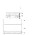
- FIG. 1 is a vertical cross-sectional view of a pn junction diode according to the first embodiment.
- FIG. 2 is a vertical sectional view of a trench type junction barrier Schottky (JBS) diode 2 according to the second embodiment.
- FIG. 3A is a vertical sectional view showing a manufacturing process of the trench type JBS diode according to the second embodiment.
- FIG. 3B is a vertical sectional view showing the manufacturing process of the trench type JBS diode according to the second embodiment.
- FIG. 3C is a vertical sectional view showing the manufacturing process of the trench type JBS diode according to the second embodiment.
- FIG. 4A is a vertical sectional view showing a manufacturing process of the trench type JBS diode according to the second embodiment.
- FIG. 4B is a vertical sectional view showing the manufacturing process of the trench type JBS diode according to the second embodiment.
- FIG. 4C is a vertical sectional view showing a manufacturing process of the trench type JBS diode according to the second embodiment.
- FIG. 5 is a vertical cross-sectional view of a Schottky barrier diode according to a third embodiment.
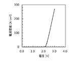
- 6A is a graph showing forward characteristics of the pn junction diode according to Example 1.
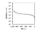
- FIG. 6B is a graph showing the reverse direction characteristic of the pn junction diode according to Example 1.
- FIG. 7A is a graph showing the substrate temperature dependence of the resistivity of the NiO film according to Example 2.
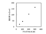
- FIG. FIG. 7B is a graph showing the plasma output dependency of the resistivity of the NiO film according to Example 2.
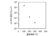
- FIG. 7C is a graph showing the substrate temperature dependence of the contact resistance between the NiO film and the Pt electrode according to Example 2.
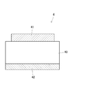
- FIG. 8 is a vertical cross-sectional view of a Schottky barrier diode according to a third embodiment.
- FIG. 9 is a graph showing the forward characteristic of the Schottky barrier diode according to the third embodiment.
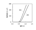
- FIG. 10A is a graph showing forward characteristics of the trench JBS diode according to Example 4.
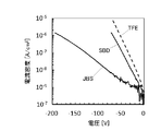
- FIG. 10B is a graph showing the reverse characteristic of the trench JBS diode according to Example 4.
- the present inventor in the case of a semiconductor element provided with an insulating film formed on a semiconductor such as a gate insulating film, the present inventor is more likely to find that the insulating film is amorphous rather than crystalline.
- the idea is that the leakage current is small, and the p-type semiconductor film that forms the hetero pn junction with the Ga 2 O 3 -based semiconductor layer has a volume of the amorphous part larger than that of the crystalline part.
- FIG. 1 is a vertical cross-sectional view of a pn junction diode 1 according to the first embodiment.
- the pn junction diode 1 is formed on an n-type semiconductor substrate 10, an n-type semiconductor layer 11 formed on the n-type semiconductor substrate 10, and a surface of the n-type semiconductor layer 11 opposite to the n-type semiconductor substrate 10.
- a cathode electrode 14 formed thereon.
- the n-type semiconductor layer 11 and the p-type semiconductor layer 12 form a pn junction, and the pn junction diode 1 utilizes the rectifying property of this pn junction.
- a voltage in the forward direction (positive potential on the anode electrode 13 side) is applied between the anode electrode 13 and the cathode electrode 14 so that the p-type semiconductor layer 12 viewed from the n-type semiconductor layer 11
- the potential barrier at the interface with the n-type semiconductor layer 11 is lowered, and a current flows from the anode electrode 13 to the cathode electrode 14.
- a voltage in the reverse direction (anode electrode 13 side has a negative potential) is applied between the anode electrode 13 and the cathode electrode 14
- no current flows due to the potential barrier between pn when a voltage in the reverse direction (anode electrode 13 side has a negative potential) is applied between the anode electrode 13 and the cathode electrode 14, no current flows due to the potential barrier between pn.
- the n-type semiconductor substrate 10 is a substrate made of an n-type Ga 2 O 3 -based single crystal.
- the n-type semiconductor substrate 10 contains donor impurities such as Si and Sn.
- the donor concentration of the n-type semiconductor substrate 10 is, for example, not less than 1.0 ⁇ 10 18 cm ⁇ 3 and not more than 1.0 ⁇ 10 20 cm ⁇ 3 .
- the thickness of the n-type semiconductor substrate 10 is, for example, 10 ⁇ m or more and 600 ⁇ m or less.
- the Ga 2 O 3 -based single crystal refers to a Ga 2 O 3 single crystal or a Ga 2 O 3 single crystal to which an element such as Al or In is added.
- an element such as Al or In
- (Ga x Al y In (1-x-y) ) 2 O 3 (0 ⁇ x ⁇ 1, 0 ⁇ y ⁇ 1, 0 ⁇ x + y ) which is a Ga 2 O 3 single crystal doped with Al and In. 1) It may be a single crystal.
- Al the band gap widens, and when In is added, the band gap narrows.
- the above-mentioned Ga 2 O 3 single crystal has, for example, a ⁇ -type crystal structure.
- the n-type semiconductor layer 11 is made of an n-type Ga 2 O 3 -based single crystal.
- the n-type semiconductor layer 11 contains donor impurities such as Si and Sn.
- the donor concentration of the n-type semiconductor layer 11 is, for example, 1 ⁇ 10 13 cm ⁇ 3 or more and 1 ⁇ 10 18 cm ⁇ 3 or less.
- the thickness of the n-type semiconductor layer 11 is, for example, not less than 1 ⁇ m and not more than 100 ⁇ m.
- the p-type semiconductor layer 12 is made of a p-type semiconductor in which the volume of the amorphous part is larger than the volume of the crystalline part.
- the p-type semiconductor for example, NiO, SnO or Cu 2 O can be used.
- NiO, SnO, and Cu 2 O exhibit p-type conductivity without the addition of a dopant, but may contain an acceptor impurity such as Li.
- NiO is thermodynamically stable, and a stable p-type can be obtained. Therefore, NiO is most preferable as the material of the p-type semiconductor layer 12.
- the formation of SnO is difficult due to the presence of Sn 2 O, which is more thermodynamically stable than SnO.
- the conductivity type of Sn 2 O is unstable and it is difficult to control it to p-type.
- the conductivity type of Cu 2 O is also unstable, and it is difficult to control it to p-type.
- the p-type semiconductor film including the amorphous portion can be formed at a lower temperature than the crystalline p-type semiconductor film as a whole, and therefore can be manufactured at low cost and easily.
- generation of a leakage current can be suppressed as compared to the case of using a p-type semiconductor film which is entirely crystalline.
- the anode electrode 13 is made of a conductive material such as Ni which forms an ohmic junction with the p-type semiconductor layer 12.
- the thickness of the anode electrode 13 is, for example, not less than 0.03 ⁇ m and not more than 5 ⁇ m.
- the portion of the cathode electrode 14 in contact with the n-type semiconductor substrate 10 is made of a conductive material such as Ti which forms an ohmic junction with the Ga 2 O 3 -based single crystal. That is, when the cathode electrode 14 has a single layer structure, the whole is made of Ti or the like, and when it has a multilayer structure, the layer in contact with the n-type semiconductor substrate 10 is made of Ti or the like. Examples of the multilayer structure of the cathode electrode 14 include Ti / Au or Ti / Al.
- the thickness of the cathode electrode 14 is, for example, not less than 0.03 ⁇ m and not more than 5 ⁇ m.
- n-type semiconductor substrate 10 a Ga 2 O 3 -based single crystal containing a donor is epitaxially grown on the n-type semiconductor substrate 10 by an HVPE (Hydride Vapor Phase Epitaxy) method or the like to form the n-type semiconductor layer 11.
- HVPE Hydrophosphide Vapor Phase Epitaxy
- the n-type semiconductor substrate 10 is obtained by slicing a bulk crystal of a Ga 2 O 3 single crystal including a donor grown by a melt growth method such as FZ (Floating Zone) method or EFG (Edge Defined Film Fed Growth) method. And a substrate obtained by polishing the surface.
- FZ Floating Zone
- EFG Edge Defined Film Fed Growth
- a p-type semiconductor is deposited on the n-type semiconductor layer 11 by radio frequency (RF) sputtering or the like so that the volume of the amorphous part is larger than the volume of the crystalline part, to form the p-type semiconductor layer 12.
- RF radio frequency
- the conditions for forming the p-type semiconductor layer 12 by high frequency sputtering are substrate temperature (deposition temperature) of 25 ° C. or more and 700 ° C. or less, plasma output of 50 W or more and 300 W or less, pressure of 0.1 Pa or more and 1 Pa or less,
- the gas species is O 2
- the gas flow rate is 0.1 sccm or more and 100 sccm or less
- the deposition time is 0.1 hours or more and 10 hours or less.
- the sputtering target is preferably made of NiO or Ni, for example, when forming the p-type semiconductor layer 12 made of NiO.
- the crystallinity of the p-type semiconductor layer 12 is considered to be affected by a plurality of parameters such as the substrate temperature and the orientation of the base crystal, but when the substrate temperature is 700 ° C. or less, the volume of the amorphous portion is crystalline. It is easy to form the p-type semiconductor layer 12 more than the volume of the quality portion.
- the anode electrode 13 and the cathode electrode 14 are formed on the surface of the p-type semiconductor layer 12 and the back surface of the n-type semiconductor substrate 10, respectively, by vacuum evaporation or the like.
- a part of the upper side of the n-type semiconductor layer 11, the p-type semiconductor layer 12, and the anode electrode 13 may be patterned in a mesa shape by photo etching or the like. By patterning in a mesa shape, it is possible to suppress a leak current flowing in the lateral direction, in particular, in the p-type semiconductor layer 12.
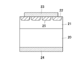
- FIG. 2 is a vertical sectional view of a trench type junction barrier Schottky (JBS) diode 2 according to the second embodiment.
- the trench type JBS diode 2 is a vertical Schottky barrier diode having a trench type junction barrier Schottky (JBS) structure.
- the trench type JBS diode 2 includes an n-type semiconductor substrate 20 and an n-type semiconductor layer 21 formed on the n-type semiconductor substrate 20 and having a trench 25 opened on the surface 26 opposite to the n-type semiconductor substrate 20.
- a cathode electrode 24 formed on the surface of the semiconductor substrate 20 opposite to the n-type semiconductor layer 21.
- the n-type semiconductor layer 21 and the anode electrode 23 form a Schottky junction, and the trench type JBS diode 2 utilizes the rectifying property of this Schottky junction.
- the upper limit of the reverse leakage current of the Schottky barrier diode is 1 ⁇ A.
- a reverse voltage when a leak current of 1 ⁇ A flows is defined as a withstand voltage.
- the current density of reverse leak current is 0.0001 A / cm 2
- the electric field strength directly under the Schottky electrode at that time is about 0.8 MV / cm, where 0.0001 A / cm 2 is when a current of 1 ⁇ A flows in the Schottky electrode of 1 mm ⁇ 1 mm in size
- the electric field strength just below the Schottky electrode is 0.8 MV / cm.
- the concentration below it is necessary to lower the donor concentration of the semiconductor layer to 10 15 cm ⁇ 3 and to make the semiconductor layer very thick. Therefore, the conduction loss becomes very large, and it is difficult to fabricate a high voltage and low loss Schottky barrier diode.
- the trench type JBS diode 2 Since the trench type JBS diode 2 according to the present embodiment has a trench type JBS structure, a high breakdown voltage can be obtained without increasing the resistance of the semiconductor layer. That is, the trench type JBS diode 2 is a Schottky barrier diode with high withstand voltage and low loss.
- the n-type semiconductor substrate 20 is made of an n-type Ga 2 O 3 -based single crystal containing a group IV element such as Si or Sn as a donor.
- the donor concentration of the n-type semiconductor substrate 20 is, for example, 1.0 ⁇ 10 18 cm ⁇ 3 or more and 1.0 ⁇ 10 20 cm ⁇ 3 or less, and the thickness of the n-type semiconductor substrate 20 is, for example, 10 ⁇ m or more. 600 ⁇ m or less.
- the n-type semiconductor layer 21 is made of an n-type Ga 2 O 3 -based single crystal containing a group IV element such as Si or Sn as a donor.
- the donor concentration of the n-type semiconductor layer 21 is lower than the donor concentration of the n-type semiconductor substrate 20.
- a high donor concentration layer containing a high concentration of donors may be formed between the n-type semiconductor substrate 20 and the n-type semiconductor layer 21. That is, the n-type semiconductor layer 21 may be stacked on the n-type semiconductor substrate 20 via the high donor concentration layer.
- the n-type semiconductor layer 21 is formed on the n-type semiconductor substrate 20 because the incorporation amount of the dopant is unstable and the acceptor impurity is diffused from the n-type semiconductor substrate 20.
- the n-type semiconductor layer 21 is grown directly, the region near the interface of the n-type semiconductor layer 21 with the n-type semiconductor substrate 20 may have a high resistance.
- high donor concentration layers are used.
- the concentration of the high donor concentration layer is set, for example, to a concentration higher than that of the n-type semiconductor layer 21, and more preferably, to a concentration higher than that of the n-type semiconductor substrate 20.
- the donor concentration of the n-type semiconductor layer 21 increases.
- the donor concentration of the n-type semiconductor layer 21 is approximately 2.0 ⁇ . It is preferably 10 17 cm -3 or less.
- the donor concentration decreases, the resistance of the n-type semiconductor layer 21 increases and the forward loss increases. Therefore, for example, when ensuring a withstand voltage of 1200 V or less, 3.0 ⁇ 10 16 cm ⁇ 3 or more Is preferred.
- the donor concentration may be lowered to, for example, about 1.0 ⁇ 10 16 cm ⁇ 3 .
- the thickness of the n-type semiconductor layer 21 increases, the maximum electric field strength in the n-type semiconductor layer 21 decreases.
- the thickness of the n-type semiconductor layer 21 is preferably about 3 ⁇ m or more and 9 ⁇ m or less.
- the electric field strength of each part of the trench type JBS diode 2 changes according to the depth D t of the trench 25.
- the depth D t of the trench 25 is about 1.5 ⁇ m or more It is preferable that it is 6 micrometers or less.
- the width Wt of the trench 25 is preferably 0.3 ⁇ m or more and 5 ⁇ m or less.
- the width W m of the mesa-shaped portion between the adjacent trenches 25 of n-type semiconductor layer 21 is reduced, the maximum electric field strength in the region immediately below the anode electrode 23 in the n-type semiconductor layer 21 is reduced.
- the width W m of the mesa-shaped portion is 5 ⁇ m or less.
- the width W m of the mesa-shaped portion is 0.25 ⁇ m or more.
- the p-type semiconductor layer 22 is made of a p-type semiconductor of p-type in which the volume of the amorphous part is larger than the volume of the crystalline part.
- the p-type semiconductor for example, NiO, SnO or Cu 2 O can be used.
- NiO, SnO, and Cu 2 O exhibit p-type conductivity without the addition of a dopant, but may contain an acceptor impurity such as Li.
- NiO is thermodynamically stable, and a stable p-type can be obtained. Therefore, NiO is most preferable as the material of the p-type semiconductor layer 22.
- the formation of SnO is difficult due to the presence of Sn 2 O, which is more thermodynamically stable than SnO.
- the conductivity type of Sn 2 O is unstable and it is difficult to control it to p-type.
- the conductivity type of Cu 2 O is also unstable, and it is difficult to control it to p-type.
- a p-type semiconductor film including an amorphous portion can be manufactured at lower cost and more easily than a p-type semiconductor film which is entirely crystalline.
- it since it is difficult to bury the crystalline p-type semiconductor film because the surface of various orientations of the Ga 2 O 3 -based single crystal is exposed on the inner surface of the trench 25, it includes an amorphous portion It is relatively easy to embed a p-type semiconductor film.
- generation of a leakage current can be suppressed as compared with the case of using a p-type semiconductor film which is entirely crystalline.
- the anode electrode 23 is made of a material in which a portion of the anode electrode 23 in contact with the n-type semiconductor layer 21 is in Schottky contact with the n-type semiconductor layer 21. That is, when the anode electrode 23 has a single-layer structure, the whole is made of a material that makes Schottky contact with the n-type semiconductor layer 21. It consists of a material in Schottky contact with the layer 21.
- the portion of the anode electrode 23 in contact with the n-type semiconductor layer 21 is made of Fe (iron), Cu (copper), Mo (molybdenum) or W (tungsten) It is preferable that
- the rising voltage of the trench JBS diode 2 is 0.4 V or more and 0.6 V or less.
- the rising voltage of the trench JBS diode 2 is 0.4 V or more and 0.7 V or less.
- the rising voltage of the trench JBS diode 2 is 0.6 V or more and 0.9 V or less.
- the electric field strength in the trench type JBS diode 2 is affected by the width W m of the mesa-shaped portion between two adjacent trenches 25 and the depth D t of the trench 25 as described above.
- the plane pattern (the plane pattern of the p-type semiconductor layer 22) is hardly affected. Therefore, the planar pattern (the planar pattern of the p-type semiconductor layer 22) of the trench 25 of the n-type semiconductor layer 21 is not particularly limited.
- the cathode electrode 24 is in ohmic contact with the n-type semiconductor substrate 20.
- the cathode electrode 24 is made of metal such as Ti.
- the cathode electrode 24 may have a multilayer structure in which different metal films are stacked, for example, Ti / Au or Ti / Al.
- the layer of the cathode electrode 24 in contact with the n-type semiconductor substrate 20 is preferably made of Ti.
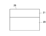
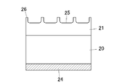
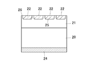
- FIGS. 3A to 3C and FIGS. 4A to 4C are vertical sectional views showing manufacturing steps of the trench type JBS diode 2 according to the second embodiment.
- a Ga 2 O 3 -based single crystal containing a donor such as Si is epitaxially grown on an n-type semiconductor substrate 20 by an HVPE method or the like to form an n-type semiconductor layer 21.
- the n-type semiconductor substrate 20 is a substrate obtained by slicing a bulk crystal of a Ga 2 O 3 -based single crystal containing a donor grown by a melt growth method such as FZ method or EFG method and polishing the surface, for example. is there.
- a trench 25 is formed on the surface 26 of the n-type semiconductor layer 21 opposite to the n-type semiconductor substrate 20 by photolithography, dry etching or the like.
- Preferred conditions for using dry etching to form the trench 25 are, for example, BCl 3 (30 sccm) as etching gas, pressure 1.0 Pa, antenna output 160 W, bias output 17 W, time 90 minutes.
- the trench 25 it is preferable to perform a treatment with phosphoric acid in order to remove roughening of the inner surface of the trench 25 and plasma damage.
- phosphoric acid heated to 130 to 140 ° C. for 1 to 30 minutes.
- the cathode electrode 24 having a Ti / Au laminated structure or the like is formed on the bottom surface of the n-type semiconductor substrate 20 by electron beam evaporation or the like. After that, heat treatment is performed at 450 ° C. for 1 minute in a nitrogen atmosphere. The heat treatment reduces the contact resistance between the cathode electrode 24 and the n-type semiconductor substrate 20.
- a p-type semiconductor film is deposited on the entire surface 26 of the n-type semiconductor layer 21 by radio-frequency sputtering or the like to such a thickness that the trench 25 can be buried.
- the conditions for forming the p-type semiconductor layer 22 by high frequency sputtering are substrate temperature (deposition temperature) of 25 ° C. to 700 ° C., plasma output of 50 W to 300 W, pressure of 0.1 Pa to 1 Pa,
- the gas species is O 2
- the gas flow rate is 0.1 sccm or more and 100 sccm or less
- the deposition time is 0.1 hours or more and 10 hours or less.
- the sputtering target is preferably made of NiO or Ni, for example, when forming the p-type semiconductor layer 22 made of NiO.
- the crystallinity of the p-type semiconductor layer 22 is considered to be affected by a plurality of parameters such as the substrate temperature and the orientation of the base crystal, but when the substrate temperature is 700 ° C. or less, the volume of the amorphous portion is crystalline. It is easy to form the p-type semiconductor layer 12 more than the volume of the quality portion.
- a portion of the deposited p-type semiconductor film outside the trench 25 is removed by planarization processing such as CMP (Chemical Mechanical Polishing). , Surface 26 is exposed. Thereby, the p-type semiconductor layer 22 is embedded in the trench 25.
- CMP Chemical Mechanical Polishing
- the surface 26 of the n-type semiconductor layer 21 is subjected to a pretreatment using a processing solution containing hydrogen peroxide such as a hydrogen peroxide solution.
- a processing solution containing hydrogen peroxide such as a hydrogen peroxide solution.
- treatment solutions containing no hydrogen peroxide such as hydrochloric acid, nitric acid, sulfuric acid, hydrofluoric acid or buffered hydrofluoric acid
- treatment with a treatment solution containing hydrogen peroxide is carried out after treatment with these treatment solutions. Do.
- the rising voltage of the trench JBS diode 2 is fixed at about 0.8 to 1.0 V regardless of the material of the anode electrode 23 There is a risk of being
- the processing solution containing hydrogen peroxide in addition to hydrogen peroxide water, for example, a solution obtained by adding an appropriate amount of hydrogen peroxide and water to an inorganic acid such as hydrochloric acid, nitric acid or sulfuric acid can be used.
- an inorganic acid such as hydrochloric acid, nitric acid or sulfuric acid
- sulfuric acid peroxide in which hydrogen peroxide and water are added to sulfuric acid
- the anode electrode 23 having a Mo / Au laminated structure or the like is formed on the surface 26 of the n-type semiconductor layer 21 by electron beam evaporation or the like.
- the anode electrode 23 is patterned into a predetermined shape such as a circle by lift-off or the like.
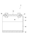
- FIG. 5 is a vertical sectional view of the Schottky barrier diode 3 according to the third embodiment.
- the Schottky barrier diode 3 is a vertical Schottky barrier diode having a guard ring structure.
- the Schottky barrier diode 3 has an n-type semiconductor substrate 30, an n-type semiconductor layer 31 formed on the n-type semiconductor substrate 30, and a trench 35 opened in a surface 36 opposite to the n-type semiconductor substrate 30.
- Semiconductor layer 31 a p-type semiconductor layer 32 as a guard ring embedded in the trench 35 of the n-type semiconductor layer 31, an anode electrode 33 formed on the surface 36 of the n-type semiconductor layer 21, n-type And a cathode electrode 34 formed on the surface of the semiconductor substrate 30 opposite to the n-type semiconductor layer 31.
- the p-type semiconductor layer 32 as a guard ring is formed in a region partially overlapping the anode electrode 33, and can relieve the concentration of the electric field at the end of the anode electrode 33 and improve the withstand voltage of the Schottky barrier diode 3. .
- the Schottky barrier diode 3 has a dielectric film 37 made of a dielectric such as SiO 2 around the anode electrode 33 on the surface 36 of the n-type semiconductor layer 31, and the dielectric film 37 is formed on the dielectric film 37.
- the edge of the anode electrode 33 runs on.
- This field plate structure can also alleviate the concentration of the electric field at the end of the anode electrode 33 and improve the breakdown voltage of the Schottky barrier diode 3.
- the n-type semiconductor layer 31 and the anode electrode 33 form a Schottky junction, and the Schottky barrier diode 3 utilizes the rectifying property of the Schottky junction.
- the Schottky barrier diode 3 by applying a forward voltage (anode electrode 33 has a positive potential) between the anode electrode 33 and the cathode electrode 34, the anode electrode 33 and n as viewed from the n-type semiconductor layer 31 The potential barrier at the interface with the semiconductor layer 31 is lowered, and a current flows from the anode electrode 33 to the cathode electrode 34.
- a forward voltage anode electrode 33 has a positive potential
- the n-type semiconductor substrate 30 is made of an n-type Ga 2 O 3 -based single crystal containing a group IV element such as Si or Sn as a donor.
- the donor concentration of the n-type semiconductor substrate 30 is, for example, 1.0 ⁇ 10 18 cm ⁇ 3 or more and 1.0 ⁇ 10 20 cm ⁇ 3 or less, and the thickness of the n-type semiconductor substrate 30 is, for example, 10 ⁇ m or more 600 ⁇ m or less.
- the n-type semiconductor layer 31 is made of an n-type Ga 2 O 3 -based single crystal containing a group IV element such as Si or Sn as a donor.
- the donor concentration of the n-type semiconductor layer 31 is lower than the donor concentration of the n-type semiconductor substrate 20.
- a high donor concentration layer containing a high concentration of donors may be formed between the n-type semiconductor substrate 30 and the n-type semiconductor layer 31. That is, the n-type semiconductor layer 21 may be stacked on the n-type semiconductor substrate 30 via the high donor concentration layer.
- the concentration of the high donor concentration layer is set, for example, to a concentration higher than that of the n-type semiconductor layer 21, and more preferably, to a concentration higher than that of the n-type semiconductor substrate 20.
- the donor concentration of the n-type semiconductor layer 31 increases.
- the donor concentration of the n-type semiconductor layer 31 is approximately 2.0 ⁇ . It is preferably 10 17 cm -3 or less.
- the donor concentration decreases, the resistance of the n-type semiconductor layer 31 increases, and the forward loss increases.
- the donor concentration may be lowered to, for example, about 1.0 ⁇ 10 15 cm ⁇ 3 .
- the thickness of the n-type semiconductor layer 31 increases, the maximum electric field strength in the n-type semiconductor layer 31 decreases.
- the thickness of the n-type semiconductor layer 31 is preferably about 3 ⁇ m or more and 15 ⁇ m or less.
- the p-type semiconductor layer 32 is made of a p-type p-type semiconductor in which the volume of the amorphous part is larger than the volume of the crystalline part.
- NiO, SnO, and Cu 2 O exhibit p-type conductivity without the addition of a dopant, but may contain an acceptor impurity such as Li.
- NiO is thermodynamically stable, and a stable p-type can be obtained. Therefore, NiO is most preferable as the material of the p-type semiconductor layer 32.
- the formation of SnO is difficult due to the presence of Sn 2 O, which is more thermodynamically stable than SnO.
- the conductivity type of Sn 2 O is unstable and it is difficult to control it to p-type.
- the conductivity type of Cu 2 O is also unstable, and it is difficult to control it to p-type.
- the p-type semiconductor film including the amorphous portion can be formed at a lower temperature than the crystalline p-type semiconductor film as a whole, and therefore can be manufactured at low cost and easily.
- it since it is difficult to bury the crystalline p-type semiconductor film since the planes of various orientations of the Ga 2 O 3 -based single crystal are exposed on the inner surface of trench 35, it includes an amorphous portion. It is relatively easy to embed a p-type semiconductor film.
- a p-type semiconductor film including an amorphous portion as the p-type semiconductor layer 32, generation of a leakage current can be suppressed as compared with the case of using a p-type semiconductor film which is entirely crystalline.
- the anode electrode 33 is made of a material in which a portion of the anode electrode 33 in contact with the n-type semiconductor layer 31 is in Schottky contact with the n-type semiconductor layer 31. That is, when the anode electrode 33 has a single-layer structure, the whole is made of a material that makes Schottky contact with the n-type semiconductor layer 31, and when it has a multilayer structure, at least the layer contacting the n-type semiconductor layer 31 is an n-type semiconductor It consists of a material in Schottky contact with the layer 31.
- the portion of the anode electrode 33 in contact with the n-type semiconductor layer 31 is made of Fe (iron), Cu (copper), Mo (molybdenum) or W (tungsten) It is preferable that
- the rising voltage of the Schottky barrier diode 3 is 0.4 V or more and 0.6 V or less.
- the portion of the anode electrode 33 in contact with the n-type semiconductor layer 31 is made of Fe
- the rising voltage of the Schottky barrier diode 3 is 0.4 V or more and 0.7 V or less.
- the portion of the anode electrode 33 in contact with the n-type semiconductor layer 31 is made of Cu
- the rising voltage of the Schottky barrier diode 3 is 0.6 V or more and 0.9 V or less.
- the cathode electrode 34 is in ohmic contact with the n-type semiconductor substrate 30.
- the cathode electrode 34 is made of metal such as Ti.
- the cathode electrode 34 may have a multilayer structure in which different metal films are stacked, for example, Ti / Au or Ti / Al.
- the layer of the cathode electrode 34 in contact with the n-type semiconductor substrate 30 is preferably made of Ti.
- the pn junction diode 1 and the trench type JBS diode 2 which are Ga 2 O 3 based diodes utilizing hetero pn junctions which can be easily manufactured at low cost And a Schottky barrier diode 3 having a guard ring structure.
- Example 1 the pn junction diode 1 according to the first embodiment was manufactured, and forward characteristics and reverse characteristics were measured.
- the n-type semiconductor substrate 10 is manufactured by using the EFG method in which the donor is Sn, the donor concentration is approximately 10 18 cm ⁇ 3 , the thickness is approximately 600 ⁇ m, and the plane orientation of the main surface is (001). An n-type Ga 2 O 3 substrate was used.
- n-type semiconductor layer 11 an n-type Ga 2 O 3 film grown by the HVPE method using Si donor, donor concentration of about 6 ⁇ 10 16 cm ⁇ 3 and thickness of about 3.2 ⁇ m was used. .
- a p-type NiO film formed by high-frequency sputtering and having a thickness of about 100 nm (without intentionally adding an acceptor) was used as the p-type semiconductor layer 12.
- the conditions for high frequency sputtering are: substrate temperature 300 ° C., plasma power 50 W, pressure 0.35 Pa, gas species O 2 , gas flow 10 sccm, target 99.5% purity NiO, deposition time 1 hour there were.
- anode electrode 13 a circular Ni electrode having a diameter of 200 ⁇ m was formed by electron beam evaporation.
- an electrode having a Ti / Au laminated structure was formed on the entire back surface of the n-type semiconductor substrate 10 by electron beam evaporation.
- dry etching is performed using the anode electrode 13 as a mask, and a portion of the upper side of the n-type semiconductor layer 11 and the p-type semiconductor layer 12 have a mesa shape as shown in FIG. Patterned.
- FIGS. 6A and 6B are graphs showing forward characteristics and reverse characteristics of the pn junction diode 1 according to the first embodiment, respectively.
- the pn junction diode 1 normally operates as a pn junction diode. This indicates that the n-type semiconductor layer 11 which is an n-type Ga 2 O 3 film and the p-type semiconductor layer 12 which is a p-type NiO film form a pn junction.
- Example 2 the film formation condition dependency of the characteristics of the NiO film was examined.
- the NiO film was formed by high frequency sputtering.
- the conditions for high frequency sputtering were a substrate temperature of 25 to 400 ° C., a plasma output of 50 to 300 W, a pressure of 0.35 Pa, a gas type of O 2 , a gas flow rate of 10 sccm, a target of NiO, and a deposition time of 1 hour.
- FIG. 7A is a graph showing the substrate temperature dependence of the resistivity of the NiO film according to Example 2.
- FIG. The NiO film which concerns on FIG. 7A fixed the plasma output to 300 W, and formed it into a film.
- FIG. 7A shows that the lower the substrate temperature, the lower the resistivity of the NiO film. From this result, it can be said that the substrate temperature at the time of forming the NiO film by high frequency sputtering is preferably 25 ° C. or more and 400 ° C. or less in order to reduce the resistivity. However, this is a result of using an undoped NiO target, and by doping the acceptor, a low resistivity film can be obtained at a temperature higher than 400 ° C.
- FIG. 7B is a graph showing the plasma output dependency of the resistivity of the NiO film according to Example 2.
- the NiO film according to FIG. 7B was formed with the substrate temperature fixed at 200 ° C.
- FIG. 7B shows that the lower the plasma output, the lower the resistivity of the NiO film. From this result, it can be said that, in order to reduce the resistivity, it is preferable that the plasma output at the time of forming the NiO film by high frequency sputtering be 50 W or more and 300 W or less.
- FIG. 7C is a graph showing the substrate temperature dependence of the contact resistance between the NiO film and the Pt electrode according to Example 2.
- the NiO film according to FIG. 7C was formed with the plasma output fixed at 300 W.
- FIG. 7C shows that the higher the substrate temperature, the lower the contact resistance. From this result, in order to reduce the contact resistance with the electrode, it can be said that the substrate temperature at the time of forming the NiO film by high frequency sputtering is preferably 100 ° C. or more.
- Example 3 the characteristics of each material of the anode electrode in the Schottky barrier diode were examined.
- FIG. 8 is a vertical cross-sectional view of the Schottky barrier diode 4 according to the third embodiment.
- the Schottky barrier diode 4 is connected to the semiconductor substrate 40 and one surface of the semiconductor substrate 40, is connected to the anode electrode 41 forming a Schottky junction with the semiconductor substrate 40, and is connected to the other surface of the semiconductor substrate 40 A cathode electrode 42 forming an ohmic junction with the substrate 40 is provided.
- an undoped Ga 2 O 3 substrate having a donor concentration of about 10 17 cm -3 and a thickness of about 650 ⁇ m was used.
- anode electrode 41 a circular electrode having a diameter of 200 ⁇ m was formed by electron beam evaporation. Before deposition of the anode electrode 41, the surface of the semiconductor substrate 40 was treated with sulfuric acid / hydrogen peroxide. As a material of the anode electrode 41, Al, Ti, Mo, W, Fe, Cu, Ni, Pt, and Pd were used.
- an electrode having a Ti / Au laminated structure in which a Ti film of 50 nm in thickness and an Au film of 200 nm in thickness are laminated is formed on a part of the back surface of the semiconductor substrate 40 by electron beam evaporation.
- FIG. 9 is a graph showing forward characteristics of the Schottky barrier diode 4 according to the third embodiment.
- FIG. 9 shows that the rising voltage of the Schottky barrier diode is about 0 V, 0.05 V, 0.35 V, 0 when the material of the anode electrode is Al, Ti, Mo, W, Fe, Cu, Ni, Pt, and Pd, respectively. 4 V, 0.55 V, 0.65 V, 0.85 V, 0.95 V, 0.95 V are shown.
- Fe, Cu, Mo, and W are used as the material of the anode electrode, since a rising voltage between Ti and Ni, which are known electrode materials, can be obtained, Fe, Cu, Mo, and W is useful as a new Schottky electrode material.
- Example 4 a trench type JBS diode 2 according to the second embodiment was manufactured and the characteristics thereof were evaluated.
- the n-type semiconductor substrate 20 As the n-type semiconductor substrate 20, an EFG method in which the donor is Sn, the donor concentration is about 2.5 ⁇ 10 18 cm ⁇ 3 , the thickness is about 350 ⁇ m, and the plane orientation of the main surface is (001) An n-type Ga 2 O 3 substrate manufactured using
- n-type semiconductor layer 21 an n-type Ga 2 O 3 film grown by the HVPE method using Si as a donor, a donor concentration of about 6 ⁇ 10 16 cm ⁇ 3 and a thickness of about 6.5 ⁇ m is used. .
- the depth D t of the trench 25 of the n-type semiconductor layer 21 is about 2 ⁇ m, the width W t of the trench 25 is about 4.8 ⁇ m, and the width W m of the mesa-shaped portion is about 1.2 ⁇ m.
- an electrode having a Ti / Au laminated structure was formed on the entire back surface of the n-type semiconductor substrate 20 by electron beam evaporation. After forming the cathode electrode 24, heat treatment was performed at 450 ° C. for 1 minute in a nitrogen atmosphere to reduce the contact resistance between the cathode electrode 24 and the n-type semiconductor substrate 20.
- an undoped p-type NiO film formed by high-frequency sputtering was used as the p-type semiconductor layer 22 as the p-type semiconductor layer 22, an undoped p-type NiO film formed by high-frequency sputtering was used.
- the conditions for high frequency sputtering are: substrate temperature 200 ° C., plasma power 300 W, pressure 0.35 Pa, gas species O 2 , gas flow rate 10 sccm, target NiO, deposition time 4 hours, approximately 3 ⁇ m NiO A film was formed. The portion outside the trench 25 of the NiO film was removed by CMP.
- an electrode having a circular Mo / Au laminated structure having a diameter of 300 ⁇ m or the like was formed by electron beam evaporation and lift-off.
- 10A and 10B are graphs showing forward characteristics and reverse characteristics of the trench JBS diode 2 according to the fourth embodiment, respectively.
- JBS in FIGS. 10A and 10B is a characteristic of the trench type JBS diode 2
- SBD is a characteristic of a normal Schottky barrier diode having no JBS structure as a comparative example.
- TFE in FIG. 10 (b) is the calculation result based on the thermionic field emission theory (the height of potential barrier is 0.8 eV, the donor concentration of the semiconductor forming the Schottky electrode and the Schottky junction is 6 ⁇ Calculated as 10 16 cm -3 ).
- the trench type JBS diode 2 normally operates as a Schottky barrier diode. This indicates that the n-type semiconductor layer 21 which is an n-type Ga 2 O 3 film and the p-type semiconductor layer 22 which is a p-type NiO film form a pn junction.
- FIG. 10B shows that the trench type JBS diode 2 is a normal Schottky while the normal Schottky barrier diode not having the JBS structure has a very large leak current close to the thermionic field emission theory. Leakage current is several orders of magnitude smaller than barrier diodes. This is because the electric field strength of the Schottky junction is lowered by providing the JBS structure, and the leak current due to thermionic field emission (TFE) can be suppressed.
- TFE thermionic field emission
- the leak characteristic conforms to the thermionic field emission theory. It may be worse than the property.
- the present invention provides a Ga 2 O 3 -based diode utilizing a hetero pn junction, which can be easily manufactured at low cost.
Landscapes
- Chemical & Material Sciences (AREA)
- Engineering & Computer Science (AREA)
- Crystallography & Structural Chemistry (AREA)
- Materials Engineering (AREA)
- Metallurgy (AREA)
- Organic Chemistry (AREA)
- Chemical Kinetics & Catalysis (AREA)
- General Chemical & Material Sciences (AREA)
- Inorganic Chemistry (AREA)
- Electrodes Of Semiconductors (AREA)
- Crystals, And After-Treatments Of Crystals (AREA)
Abstract
低コストで容易に製造することのできる、ヘテロpn接合を利用したGa2O3系のダイオードを提供する。 一実施の形態として、n型Ga2O3系単結晶からなるn型半導体層21と、非晶質部分の体積が結晶質部分の体積よりも多いp型半導体からなるp型半導体層22と、を備え、n型半導体層21とp型半導体層22とがpn接合を形成する、ダイオード2を提供する。
Description
本発明は、ダイオードに関する。
従来、p型のGa2O3の形成が困難であることが知られている。このため、Ga2O3系のダイオードにおいてホモpn接合を形成することは難しいと考えられている。
一方で、n型のβ-Ga2O3単結晶がp型のNiO単結晶とヘテロpn接合を形成することが知られている(例えば、非特許文献1参照)。特許文献1には、n型のβ-Ga2O3単結晶とp型のNiO単結晶とによるヘテロpn接合の整流性を利用したpn接合ダイオードが開示されている。
また、n型のα-Ga2O3結晶とp型の六方晶の結晶構造を有する無機化合物結晶とによるヘテロpn接合を利用したジャンクションバリアショットキー構造やガードリング構造を有するショットキーバリアダイオードが知られている(例えば、特許文献1参照)。
Yoshihiro Kokubun et al., "All-oxide p-n heterojunction diodes comprising p-type NiO and n-type β-Ga2O3", Applied Physics Express 9, 091101 (2016)
本発明の目的は、低コストで容易に製造することのできる、ヘテロpn接合を利用したGa2O3系のダイオードを提供することにある。
本発明の一態様は、上記目的を達成するために、下記[1]~[6]のダイオードを提供する。
[1]n型Ga2O3系単結晶からなるn型半導体層と、非晶質部分の体積が結晶質部分の体積よりも多いp型半導体からなるp型半導体層と、を備え、前記n型半導体層と前記p型半導体層とがpn接合を形成する、ダイオード。
[2]前記p型半導体がNiOである、上記[1]に記載のダイオード。
[3]前記pn接合の整流性を利用したpn接合ダイオードである、上記[1]又は[2]に記載のダイオード。
[4]n型半導体層とショットキー接合を形成するアノード電極を備え、前記ショットキー接合の整流性を利用するショットキーバリアダイオードである、上記[1]又は[2]に記載のダイオード。
[5]トレンチ型ジャンクションバリアショットキー構造又はガードリング構造を有する、上記[4]に記載のダイオード。
[6]前記アノード電極の前記n型半導体層と接触する部分がFe、Cu、Mo、又はWからなる、上記[4]又は[5]に記載のダイオード。
本発明によれば、低コストで容易に製造することのできる、ヘテロpn接合を利用したGa2O3系のダイオードを提供することができる。
本発明は、本発明者が、ゲート絶縁膜等の半導体上に形成される絶縁膜を備えた半導体素子においては、絶縁膜が結晶質である場合よりも非晶質である場合の方が、リーク電流が小さくなるということから着想を得て、Ga2O3系半導体層とヘテロpn接合を形成するp型半導体膜に、非晶質部分の体積が結晶質部分の体積よりも多いp型半導体膜を用いたことに端を発する。
以下、Ga2O3系半導体層と非晶質部分の体積が結晶質部分の体積よりも多いp型半導体膜とのヘテロpn接合を利用した半導体素子の具体例について説明する。
〔第1の実施の形態〕
(pn接合ダイオードの構成)
図1は、第1の実施の形態に係るpn接合ダイオード1の垂直断面図である。pn接合ダイオード1は、n型半導体基板10と、n型半導体基板10上に形成されたn型半導体層11と、n型半導体層11のn型半導体基板10と反対側の面上に形成されたp型半導体層12と、p型半導体層12のn型半導体層11と反対側の面上に形成されたアノード電極13と、n型半導体基板10のn型半導体層11と反対側の面上に形成されたカソード電極14と、を備える。
(pn接合ダイオードの構成)
図1は、第1の実施の形態に係るpn接合ダイオード1の垂直断面図である。pn接合ダイオード1は、n型半導体基板10と、n型半導体基板10上に形成されたn型半導体層11と、n型半導体層11のn型半導体基板10と反対側の面上に形成されたp型半導体層12と、p型半導体層12のn型半導体層11と反対側の面上に形成されたアノード電極13と、n型半導体基板10のn型半導体層11と反対側の面上に形成されたカソード電極14と、を備える。
n型半導体層11とp型半導体層12とは、pn接合を形成し、pn接合ダイオード1は、このpn接合の整流性を利用している。
pn接合ダイオード1においては、アノード電極13とカソード電極14との間に順方向の電圧(アノード電極13側が正電位)を印加することにより、n型半導体層11から見たp型半導体層12とn型半導体層11との界面のポテンシャル障壁が低下し、アノード電極13からカソード電極14へ電流が流れる。一方、アノード電極13とカソード電極14との間に逆方向の電圧(アノード電極13側が負電位)を印加したときは、pn間のポテンシャル障壁により、電流が流れない。
n型半導体基板10は、n型のGa2O3系単結晶からなる基板である。n型半導体基板10は、Si、Sn等のドナー不純物を含む。n型半導体基板10のドナー濃度は、例えば、1.0×1018cm-3以上かつ1.0×1020cm-3以下である。n型半導体基板10の厚さは、例えば、10μm以上かつ600μm以下である。
ここで、Ga2O3系単結晶とは、Ga2O3単結晶、又は、Al、In等の元素が添加されたGa2O3単結晶をいう。例えば、Al及びInが添加されたGa2O3単結晶である(GaxAlyIn(1-x-y))2O3(0<x≦1、0≦y<1、0<x+y≦1)単結晶であってもよい。Alを添加した場合にはバンドギャップが広がり、Inを添加した場合にはバンドギャップが狭くなる。なお、上記のGa2O3単結晶は、例えば、β型の結晶構造を有する。
n型半導体層11は、n型のGa2O3系単結晶からなる。n型半導体層11は、Si、Sn等のドナー不純物を含む。n型半導体層11のドナー濃度は、例えば、1×1013cm-3以上かつ1×1018cm-3以下である。n型半導体層11の厚さは、例えば、1μm以上かつ100μm以下である。
p型半導体層12は、非晶質部分の体積が結晶質部分の体積よりも多いp型半導体からなる。p型半導体としては、例えば、NiO、SnO、又はCu2Oを用いることができる。NiO、SnO、Cu2Oはドーパントを添加しなくてもp型の導電性を示すが、Li等のアクセプター不純物を含んでもよい。
NiO、SnO、Cu2Oのうち、NiOは熱力学的に安定であり、かつ安定してp型のものが得られるため、p型半導体層12の材料として最も好ましい。SnOは、SnOよりも熱力学的に安定であるSn2Oが存在するため、形成が困難である。なお、Sn2Oは導電型が不安定であり、p型に制御することが難しい。また、Cu2Oも導電型が不安定であり、p型に制御することが難しい。
非晶質部分を含むp型半導体膜は、全体が結晶質のp型半導体膜よりも低温で成膜できるため、低コストかつ容易に製造することができる。また、非晶質部分を含むp型半導体膜をp型半導体層12として用いることにより、全体が結晶質のp型半導体膜を用いる場合よりも、リーク電流の発生を抑えることができる。
アノード電極13は、p型半導体層12とオーミック接合を形成するNi等の導電性材料からなる。アノード電極13の厚さは、例えば、0.03μm以上かつ5μm以下である。
カソード電極14は、n型半導体基板10と接触する部分がGa2O3系単結晶とオーミック接合を形成するTi等の導電性材料からなる。すなわち、カソード電極14が単層構造を有する場合はその全体がTi等からなり、多層構造を有する場合はn型半導体基板10と接触する層がTi等からなる。カソード電極14の多層構造としては、例えば、Ti/Au又はTi/Alが挙げられる。カソード電極14の厚さは、例えば、0.03μm以上かつ5μm以下である。
(pn接合ダイオードの製造方法)
以下に、pn接合ダイオード1の製造方法の一例について説明する。
以下に、pn接合ダイオード1の製造方法の一例について説明する。
まず、n型半導体基板10上に、HVPE(Hydride Vapor Phase Epitaxy)法等によりドナーを含むGa2O3系単結晶をエピタキシャル成長させ、n型半導体層11を形成する。
n型半導体基板10は、例えば、FZ(Floating Zone)法やEFG(Edge Defined Film Fed Growth)法等の融液成長法により育成したドナーを含むGa2O3系単結晶のバルク結晶をスライスし、表面を研磨することにより得られる基板である。
次に、n型半導体層11上に、高周波(RF)スパッタリング等により非晶質部分の体積が結晶質部分の体積よりも多いp型半導体を堆積させ、p型半導体層12を形成する。
高周波スパッタリングによりp型半導体層12を形成する場合の条件は、基板温度(堆積温度)が25℃以上かつ700℃以下、プラズマ出力が50W以上かつ300W以下、圧力が0.1Pa以上かつ1Pa以下、ガス種がO2、ガス流量が0.1sccm以上かつ100sccm以下、堆積時間が0.1時間以上かつ10時間以下であることが好ましい。スパッタリングターゲットは、例えば、NiOからなるp型半導体層12を形成する場合は、NiO又はNiからなることが好ましい。
p型半導体層12の結晶化度は、基板温度や下地結晶の方位等の複数のパラメータに影響を受けると考えられるが、基板温度が700℃以下である場合は非晶質部分の体積が結晶質部分の体積よりも多いp型半導体層12を形成しやすい。
次に、真空蒸着等により、p型半導体層12の表面及びn型半導体基板10の裏面に、それぞれアノード電極13とカソード電極14を形成する。
図1に示されるように、n型半導体層11の上側の一部、p型半導体層12、及びアノード電極13は、フォトエッチング等によりメサ形状にパターニングされてもよい。メサ形状にパターニングすることで、特にp型半導体層12中を横方向に流れるリーク電流を抑制することができる。
〔第2の実施の形態〕
(ジャンクションバリアショットキーダイオードの構成)
図2は、第2の実施の形態に係るトレンチ型ジャンクションバリアショットキー(JBS)ダイオード2の垂直断面図である。トレンチ型JBSダイオード2は、トレンチ型ジャンクションバリアショットキー(JBS)構造を有する縦型のショットキーバリアダイオードである。
(ジャンクションバリアショットキーダイオードの構成)
図2は、第2の実施の形態に係るトレンチ型ジャンクションバリアショットキー(JBS)ダイオード2の垂直断面図である。トレンチ型JBSダイオード2は、トレンチ型ジャンクションバリアショットキー(JBS)構造を有する縦型のショットキーバリアダイオードである。
トレンチ型JBSダイオード2は、n型半導体基板20と、n型半導体基板20上に形成された、n型半導体基板20と反対側の面26に開口するトレンチ25を有するn型半導体層21と、n型半導体層21のトレンチ25内に埋め込まれたp型半導体層22と、n型半導体層21の面26上にp型半導体層22と接触するように形成されたアノード電極23と、n型半導体基板20のn型半導体層21と反対側の面上に形成されたカソード電極24と、を備える。
n型半導体層21とアノード電極23とは、ショットキー接合を形成し、トレンチ型JBSダイオード2は、このショットキー接合の整流性を利用している。
トレンチ型JBSダイオード2においては、アノード電極23とカソード電極24との間に順方向の電圧(アノード電極23側が正電位)を印加することにより、n型半導体層21から見たアノード電極23とn型半導体層21との界面のポテンシャル障壁が低下し、アノード電極23からカソード電極24へ電流が流れる。
一方、アノード電極23とカソード電極24との間に逆方向の電圧(アノード電極23側が負電位)を印加したときは、ショットキー障壁により、電流は流れない。このとき、p型半導体層22から空乏層が広がり、隣接するp型半導体層22間のチャネルが閉じるため、リーク電流が効果的に抑制される。
一般的に、ショットキーバリアダイオードの逆方向リーク電流の上限は1μAとされている。本実施の形態では、1μAのリーク電流が流れるときの逆方向電圧を耐圧と定義する。
例えば、“松波弘之、大谷昇、木本恒暢、中村孝著、「半導体SiC技術と応用」、第2版、日刊工業新聞社、2011年9月30日、p.355”に記載された、SiCを半導体層とするショットキーバリアダイオードにおける逆方向リーク電流のショットキー界面電界強度依存性のデータによれば、逆方向リーク電流の電流密度が0.0001A/cm2のときのショットキー電極直下の電界強度は、およそ0.8MV/cmである。ここで、0.0001A/cm2は、サイズが1mm×1mmであるショットキー電極に1μAの電流が流れたときのショットキー電極直下の電流密度である。
このため、半導体材料自体の絶縁破壊電界強度が数MV/cmあったとしても、ショットキー電極直下の電界強度が0.8MV/cmを超えると、1μAを超えるリーク電流が流れることになる。
例えば、ショットキー電極直下の電界強度を抑制するための特別な構造を有さない従来のショットキーバリアダイオードにおいて1200Vの耐圧を得るためには、ショットキー電極直下の電界強度を0.8MV/cm以下に抑えるために、半導体層のドナー濃度を1015cm-3台にまで下げ、かつ半導体層を非常に厚くする必要がある。そのため、導通損失が非常に大きくなり、高耐圧かつ低損失のショットキーバリアダイオードを作製することは困難である。
本実施の形態に係るトレンチ型JBSダイオード2は、トレンチ型JBS構造を有するため、半導体層の抵抗を増加することなく、高い耐圧を得ることができる。すなわち、トレンチ型JBSダイオード2は、高耐圧かつ低損失のショットキーバリアダイオードである。
n型半導体基板20は、ドナーとしてのSi、Sn等のIV族元素を含むn型のGa2O3系単結晶からなる。n型半導体基板20のドナー濃度は、例えば、1.0×1018cm-3以上かつ1.0×1020cm-3以下であるn型半導体基板20の厚さは、例えば、10μm以上かつ600μm以下である。
n型半導体層21は、ドナーとしてのSi、Sn等のIV族元素を含むn型のGa2O3系単結晶からなる。n型半導体層21のドナー濃度は、n型半導体基板20のドナー濃度よりも低い。
なお、n型半導体基板20とn型半導体層21との間に、高濃度のドナーを含む高ドナー濃度層を形成してもよい。すなわち、高ドナー濃度層を介してn型半導体層21をn型半導体基板20上に積層してもよい。n型半導体層21の成長初期は、ドーパントの取り込み量が不安定であったり、n型半導体基板20からのアクセプター不純物の拡散があったりするため、n型半導体基板20上にn型半導体層21を直接成長させると、n型半導体層21のn型半導体基板20との界面に近い領域が高抵抗化する場合がある。このような問題を避けるため、高ドナー濃度層が用いられる。高ドナー濃度層の濃度は、例えば、n型半導体層21よりも高い濃度に設定され、より好ましくは、n型半導体基板20よりも高い濃度に設定される。
n型半導体層21のドナー濃度が増加するほど、トレンチ型JBSダイオード2の各部の電界強度が増加する。n型半導体層21中のアノード電極23直下の領域中の最大電界強度及びn型半導体層21中の最大電界強度を低く抑えるためには、n型半導体層21のドナー濃度がおよそ2.0×1017cm-3以下であることが好ましい。一方、ドナー濃度が小さくなるほどn型半導体層21の抵抗が大きくなり、順方向損失が増加してしまうため、例えば1200V以下の耐圧を確保する場合には、3.0×1016cm-3以上であることが好ましい。また、より高い耐圧を得るためには、ドナー濃度を例えば1.0×1016cm-3程度まで下げてもよい。
n型半導体層21の厚さが増加するほど、n型半導体層21中の最大電界強度が低減する。n型半導体層21の厚さをおよそ3μm以上にすることにより、n型半導体層21中の最大電界強度を効果的に低減することができる。これらの電界強度の低減と、トレンチ型JBSダイオード2の小型化の観点から、n型半導体層21の厚さはおよそ3μm以上かつ9μm以下であることが好ましい。
トレンチ25の深さDtによってトレンチ型JBSダイオード2の各部の電界強度が変化する。n型半導体層21中のアノード電極23直下の領域中の最大電界強度及びn型半導体層21中の最大電界強度を低く抑えるためには、トレンチ25の深さDtがおよそ1.5μm以上かつ6μm以下であることが好ましい。
トレンチ25の幅Wtは、狭いほど導通損失を低減できるが、狭いほど製造難易度が上がり、それに起因して製造歩留まりが低下するため、0.3μm以上かつ5μm以下であることが好ましい。
n型半導体層21の隣接するトレンチ25の間のメサ形状部分の幅Wmが低減するほど、n型半導体層21中のアノード電極23直下の領域中の最大電界強度が低減する。n型半導体層21中のアノード電極23直下の領域中の最大電界強度を低く抑えるためには、メサ形状部分の幅Wmが5μm以下であることが好ましい。一方、メサ形状部分の幅が小さいほどトレンチ25の製造難度が上がるため、メサ形状部分の幅Wmが0.25μm以上であることが好ましい。
p型半導体層22は、非晶質部分の体積が結晶質部分の体積よりも多いp型のp型半導体からなる。p型半導体としては、例えば、NiO、SnO、又はCu2Oを用いることができる。NiO、SnO、Cu2Oはドーパントを添加しなくてもp型の導電性を示すが、Li等のアクセプター不純物を含んでもよい。
NiO、SnO、Cu2Oのうち、NiOは熱力学的に安定であり、かつ安定してp型のものが得られるため、p型半導体層22の材料として最も好ましい。SnOは、SnOよりも熱力学的に安定であるSn2Oが存在するため、形成が困難である。なお、Sn2Oは導電型が不安定であり、p型に制御することが難しい。また、Cu2Oも導電型が不安定であり、p型に制御することが難しい。
非晶質部分を含むp型半導体膜は、全体が結晶質のp型半導体膜よりも、低コストかつ容易に製造することができる。特に、トレンチ25の内面にはGa2O3系単結晶の様々な方位の面が露出しているため、結晶性のp型半導体膜を埋め込むことは困難であるが、非晶質部分を含むp型半導体膜を埋め込むことは比較的容易である。また、非晶質部分を含むp型半導体膜をp型半導体層22として用いることにより、全体が結晶質のp型半導体膜を用いる場合よりも、リーク電流の発生を抑えることができる。
アノード電極23は、アノード電極23のn型半導体層21と接触する部分がn型半導体層21とショットキー接触する材料からなる。すなわち、アノード電極23が単層構造を有する場合はその全体がn型半導体層21とショットキー接触する材料からなり、多層構造を有する場合は少なくともn型半導体層21と接触する層がn型半導体層21とショットキー接触する材料からなる。
トレンチ型JBSダイオード2の立ち上がり電圧を小さくするためには、アノード電極23のn型半導体層21と接触する部分がFe(鉄)、Cu(銅)、Mo(モリブデン)、又はW(タングステン)からなることが好ましい。
アノード電極23のn型半導体層21と接触する部分がMo又はWからなる場合、トレンチ型JBSダイオード2の立ち上がり電圧は0.4V以上かつ0.6V以下となる。アノード電極23のn型半導体層21と接触する部分がFeからなる場合は、トレンチ型JBSダイオード2の立ち上がり電圧は0.4V以上かつ0.7V以下となる。また、アノード電極23のn型半導体層21と接触する部分がCuからなる場合、トレンチ型JBSダイオード2の立ち上がり電圧は0.6V以上かつ0.9V以下となる。
トレンチ型JBSダイオード2においては、メサ形状部分にポテンシャル障壁が形成されるため、立ち上がり電圧はメサ形状部分の幅Wmに依存し、幅Wmが小さくなるほど大きくなる。
トレンチ型JBSダイオード2中の電界強度は、上述のように、隣接する2つのトレンチ25の間のメサ形状部分の幅Wm、トレンチ25の深さDt等の影響を受けるが、トレンチ25の平面パターン(p型半導体層22の平面パターン)にはほとんど影響を受けない。このため、n型半導体層21のトレンチ25の平面パターン(p型半導体層22の平面パターン)は特に限定されない。
カソード電極24は、n型半導体基板20とオーミック接触する。カソード電極24は、Ti等の金属からなる。カソード電極24は、異なる金属膜を積層した多層構造、例えば、Ti/Au又はTi/Al、を有してもよい。カソード電極24とn型半導体基板20を確実にオーミック接触させるため、カソード電極24のn型半導体基板20と接触する層がTiからなることが好ましい。
(トレンチ型JBSダイオードの製造方法)
以下に、トレンチ型JBSダイオード2の製造方法の一例を示す。
以下に、トレンチ型JBSダイオード2の製造方法の一例を示す。
図3A~図3C、図4A~図4Cは、第2の実施の形態に係るトレンチ型JBSダイオード2の製造工程を示す垂直断面図である。
まず、図3Aに示されるように、n型半導体基板20上に、HVPE法等によりSi等のドナーを含むGa2O3系単結晶をエピタキシャル成長させ、n型半導体層21を形成する。
n型半導体基板20は、例えば、FZ法やEFG法等の融液成長法により育成したドナーを含むGa2O3系単結晶のバルク結晶をスライスし、表面を研磨することにより得られる基板である。
次に、図3Bに示されるように、フォトリソグラフィとドライエッチング等によりn型半導体層21のn型半導体基板20と反対側の面26にトレンチ25を形成する。
トレンチ25の形成にドライエッチングを用いる場合の好ましい条件は、例えば、エッチングガスがBCl3(30sccm)、圧力が1.0Pa、アンテナ出力が160W、バイアス出力が17W、時間が90分である。
また、トレンチ25の形成後、トレンチ25の内面の荒れやプラズマダメージを除去するため、リン酸での処理を行うことが好ましい。典型的には、130~140℃に加熱したリン酸へ1~30分浸漬することが好ましい。
次に、図3Cに示されるように、電子ビーム蒸着等により、n型半導体基板20の底面にTi/Au積層構造等を有するカソード電極24を形成する。その後、窒素雰囲気中で450℃1分の加熱処理を行う。この加熱処理によって、カソード電極24とn型半導体基板20の間のコンタクト抵抗が減少する。
次に、図4Aに示されるように、高周波スパッタリング等により、n型半導体層21の面26の全面に、トレンチ25を埋め込める程度の厚さのp型半導体膜を堆積させる。
高周波スパッタリングによりp型半導体層22を形成する場合の条件は、基板温度(堆積温度)が25℃以上かつ700℃以下、プラズマ出力が50W以上かつ300W以下、圧力が0.1Pa以上かつ1Pa以下、ガス種がO2、ガス流量が0.1sccm以上かつ100sccm以下、堆積時間が0.1時間以上かつ10時間以下であることが好ましい。スパッタリングターゲットは、例えば、NiOからなるp型半導体層22を形成する場合は、NiO又はNiからなることが好ましい。
p型半導体層22の結晶化度は、基板温度や下地結晶の方位等の複数のパラメータに影響を受けると考えられるが、基板温度が700℃以下である場合は非晶質部分の体積が結晶質部分の体積よりも多いp型半導体層12を形成しやすい。
次に、図4Bに示されるように、CMP(Chemical Mechanical Polishing)等の平坦化処理により、堆積させたp型半導体膜のトレンチ25の外側の部分(面26よりも上の部分)を除去し、面26を露出させる。これにより、トレンチ25内にp型半導体層22が埋め込まれる。
その後、アノード電極23の形成の前に、n型半導体層21の面26に、過酸化水素水等の過酸化水素を含む処理液を用いた前処理を施す。また、塩酸、硝酸、硫酸、フッ酸、バッファードフッ酸等の過酸化水素を含まない処理液を用いる場合は、それらの処理液による処理の後に過酸化水素を含む処理液を用いた処理を行う。前処理の最後に過酸化水素を含む処理液を用いた処理を行わない場合、アノード電極23の材料に依存せずにトレンチ型JBSダイオード2の立ち上がり電圧が0.8~1.0V程度に固定されてしまうおそれがある。
過酸化水素を含む処理液としては、過酸化水素水の他に、例えば、塩酸、硝酸、硫酸等の無機酸に過酸化水素及び水を適量添加した液を用いることができる。例えば、硫酸に過酸化水素及び水が添加された硫酸過水を用いる場合には、硫酸4に対して過酸化水素を1、水を1~1000の体積比率で混合した硫酸過水を用いることができる。
次に、図4Cに示されるように、電子ビーム蒸着等により、n型半導体層21の面26上にMo/Au積層構造等を有するアノード電極23を形成する。アノード電極23は、リフトオフ等により、円形等の所定の形状にパターニングされる。
〔第3の実施の形態〕
(ショットキーバリアダイオードの構成)
図5は、第3の実施の形態に係るショットキーバリアダイオード3の垂直断面図である。ショットキーバリアダイオード3は、ガードリング構造を有する縦型のショットキーバリアダイオードである。
(ショットキーバリアダイオードの構成)
図5は、第3の実施の形態に係るショットキーバリアダイオード3の垂直断面図である。ショットキーバリアダイオード3は、ガードリング構造を有する縦型のショットキーバリアダイオードである。
ショットキーバリアダイオード3は、n型半導体基板30と、n型半導体基板30上に形成されたn型半導体層31と、n型半導体基板30と反対側の面36に開口するトレンチ35を有するn型半導体層31と、n型半導体層31のトレンチ35内に埋め込まれたガードリングとしてのp型半導体層32と、n型半導体層21の面36上に形成されたアノード電極33と、n型半導体基板30のn型半導体層31と反対側の面上に形成されたカソード電極34と、を有する。
ガードリングとしてのp型半導体層32は、アノード電極33に一部が重なる領域に形成され、アノード電極33の端部における電界集中を緩和し、ショットキーバリアダイオード3の耐圧を向上させることができる。
また、ショットキーバリアダイオード3は、n型半導体層31の面36上のアノード電極33の周りに、SiO2等の誘電体からなる誘電体膜37を有し、その誘電体膜37の上にアノード電極33の縁が乗り上げている。このフィールドプレート構造も、アノード電極33の端部における電界集中を緩和し、ショットキーバリアダイオード3の耐圧を向上させることができる。
n型半導体層31とアノード電極33とは、ショットキー接合を形成し、ショットキーバリアダイオード3は、このショットキー接合の整流性を利用している。
ショットキーバリアダイオード3においては、アノード電極33とカソード電極34との間に順方向の電圧(アノード電極33側が正電位)を印加することにより、n型半導体層31から見たアノード電極33とn型半導体層31との界面のポテンシャル障壁が低下し、アノード電極33からカソード電極34へ電流が流れる。
一方、アノード電極33とカソード電極34との間に逆方向の電圧(アノード電極23側が負電位)を印加したときは、ショットキー障壁により、電流が流れない。また、このとき、ガードリング構造及びフィールドプレート構造により、アノード電極33の端部への電界集中が緩和され、リーク電流が抑制される。
n型半導体基板30は、ドナーとしてのSi、Sn等のIV族元素を含むn型のGa2O3系単結晶からなる。n型半導体基板30のドナー濃度は、例えば、1.0×1018cm-3以上かつ1.0×1020cm-3以下であるn型半導体基板30の厚さは、例えば、10μm以上かつ600μm以下である。
n型半導体層31は、ドナーとしてのSi、Sn等のIV族元素を含むn型のGa2O3系単結晶からなる。n型半導体層31のドナー濃度は、n型半導体基板20のドナー濃度よりも低い。
なお、n型半導体基板30とn型半導体層31との間に、高濃度のドナーを含む高ドナー濃度層を形成してもよい。すなわち、高ドナー濃度層を介してn型半導体層21をn型半導体基板30上に積層してもよい。高ドナー濃度層の濃度は、例えば、n型半導体層21よりも高い濃度に設定され、より好ましくは、n型半導体基板20よりも高い濃度に設定される。
n型半導体層31のドナー濃度が増加するほど、ショットキーバリアダイオード3の各部の電界強度が増加する。n型半導体層31中のアノード電極33直下の領域中の最大電界強度及びn型半導体層31中の最大電界強度を低く抑えるためには、n型半導体層31のドナー濃度がおよそ2.0×1017cm-3以下であることが好ましい。一方、ドナー濃度が小さくなるほどn型半導体層31の抵抗が大きくなり、順方向損失が増加してしまうため、例えば1200V以下の耐圧を確保する場合には、6.0×1015cm-3以上であることが好ましい。また、より高い耐圧を得るためには、ドナー濃度を例えば1.0×1015cm-3程度まで下げてもよい。
n型半導体層31の厚さが増加するほど、n型半導体層31中の最大電界強度が低減する。n型半導体層31の厚さをおよそ3μm以上にすることにより、n型半導体層31中の最大電界強度を効果的に低減することができる。これらの電界強度の低減と、ショットキーバリアダイオード3の小型化の観点から、n型半導体層31の厚さはおよそ3μm以上かつ15μm以下であることが好ましい。
p型半導体層32は、非晶質部分の体積が結晶質部分の体積よりも多いp型のp型半導体からなる。NiO、SnO、Cu2Oはドーパントを添加しなくてもp型の導電性を示すが、Li等のアクセプター不純物を含んでもよい。
NiO、SnO、Cu2Oのうち、NiOは熱力学的に安定であり、かつ安定してp型のものが得られるため、p型半導体層32の材料として最も好ましい。SnOは、SnOよりも熱力学的に安定であるSn2Oが存在するため、形成が困難である。なお、Sn2Oは導電型が不安定であり、p型に制御することが難しい。また、Cu2Oも導電型が不安定であり、p型に制御することが難しい。
非晶質部分を含むp型半導体膜は、全体が結晶質のp型半導体膜よりも低温で成膜できるため、低コストかつ容易に製造することができる。特に、トレンチ35の内面にはGa2O3系単結晶の様々な方位の面が露出しているため、結晶性のp型半導体膜を埋め込むことは困難であるが、非晶質部分を含むp型半導体膜を埋め込むことは比較的容易である。また、非晶質部分を含むp型半導体膜をp型半導体層32として用いることにより、全体が結晶質のp型半導体膜を用いる場合よりも、リーク電流の発生を抑えることができる。
アノード電極33は、アノード電極33のn型半導体層31と接触する部分がn型半導体層31とショットキー接触する材料からなる。すなわち、アノード電極33が単層構造を有する場合はその全体がn型半導体層31とショットキー接触する材料からなり、多層構造を有する場合は少なくともn型半導体層31と接触する層がn型半導体層31とショットキー接触する材料からなる。
ショットキーバリアダイオード3の立ち上がり電圧を小さくするためには、アノード電極33のn型半導体層31と接触する部分がFe(鉄)、Cu(銅)、Mo(モリブデン)、又はW(タングステン)からなることが好ましい。
アノード電極33のn型半導体層31と接触する部分がMo又はWからなる場合、ショットキーバリアダイオード3の立ち上がり電圧は0.4V以上かつ0.6V以下となる。アノード電極33のn型半導体層31と接触する部分がFeからなる場合は、ショットキーバリアダイオード3の立ち上がり電圧は0.4V以上かつ0.7V以下となる。また、アノード電極33のn型半導体層31と接触する部分がCuからなる場合、ショットキーバリアダイオード3の立ち上がり電圧は0.6V以上かつ0.9V以下となる。
カソード電極34は、n型半導体基板30とオーミック接触する。カソード電極34は、Ti等の金属からなる。カソード電極34は、異なる金属膜を積層した多層構造、例えば、Ti/Au又はTi/Al、を有してもよい。カソード電極34とn型半導体基板30を確実にオーミック接触させるため、カソード電極34のn型半導体基板30と接触する層がTiからなることが好ましい。
(実施の形態の効果)
上記第1~3の実施の形態によれば、低コストで容易に製造することのできる、ヘテロpn接合を利用したGa2O3系のダイオードである、pn接合ダイオード1、トレンチ型JBSダイオード2、及びガードリング構造を有するショットキーバリアダイオード3を提供することができる。
上記第1~3の実施の形態によれば、低コストで容易に製造することのできる、ヘテロpn接合を利用したGa2O3系のダイオードである、pn接合ダイオード1、トレンチ型JBSダイオード2、及びガードリング構造を有するショットキーバリアダイオード3を提供することができる。
実施例1においては、第1の実施の形態に係るpn接合ダイオード1を製造し、順方向特性及び逆方向特性を測定した。
本実施例においては、n型半導体基板10として、ドナーがSn、ドナー濃度がおよそ1018cm-3、厚さがおよそ600μm、主面の面方位が(001)の、EFG法を用いて作製したn型Ga2O3基板を用いた。
また、n型半導体層11として、ドナーがSi、ドナー濃度がおよそ6×1016cm-3、厚さがおよそ3.2μmの、HVPE法により成長させたn型Ga2O3膜を用いた。
また、p型半導体層12として、厚さがおよそ100nmのアンドープ(アクセプターを意図的に添加していない)の、高周波スパッタリングにより形成されたp型NiO膜を用いた。高周波スパッタリングの条件は、基板温度が300℃、プラズマ出力が50W、圧力が0.35Pa、ガス種がO2、ガス流量が10sccm、ターゲットが純度99.5%のNiO、堆積時間が1時間であった。
また、アノード電極13として、直径が200μmの円形のNi電極を電子ビーム蒸着により形成した。
また、カソード電極14として、Ti/Au積層構造を有する電極を電子ビーム蒸着によりn型半導体基板10の裏面の全面に形成した。アノード電極13とカソード電極14を形成した後、アノード電極13をマスクとしてドライエッチング処理を行い、n型半導体層11の上側の一部及びp型半導体層12を図1に示したようなメサ形状にパターニングした。
図6A、図6Bは、それぞれ実施例1に係るpn接合ダイオード1の順方向特性、逆方向特性を示すグラフである。
図6A、図6Bによれば、実施例1に係るpn接合ダイオード1がpn接合ダイオードとして正常に動作している。このことは、n型Ga2O3膜であるn型半導体層11とp型NiO膜であるp型半導体層12がpn接合を形成していることを示している。
実施例2においては、NiO膜の特性の成膜条件依存性を調べた。
本実施例においては、高周波スパッタリングによりNiO膜を形成した。高周波スパッタリングの条件は、基板温度が25~400℃、プラズマ出力が50~300W、圧力が0.35Pa、ガス種がO2、ガス流量が10sccm、ターゲットがNiO、堆積時間が1時間とした。
図7Aは、実施例2に係るNiO膜の抵抗率の基板温度依存性を示すグラフである。図7Aに係るNiO膜は、プラズマ出力を300Wに固定して成膜した。
図7Aは、基板温度が低いほど、NiO膜の抵抗率が低下することを示している。この結果から、抵抗率を小さくするためには、NiO膜を高周波スパッタリングにより成膜する際の基板温度が25℃以上かつ400℃以下であることが好ましいといえる。しかしながら、これはアンドープのNiOターゲットを用いた場合の結果であり、アクセプターをドープすることで400℃より高い温度で低抵抗率の膜を得ることができる。
図7Bは、実施例2に係るNiO膜の抵抗率のプラズマ出力依存性を示すグラフである。図7Bに係るNiO膜は、基板温度を200℃に固定して成膜した。
図7Bは、プラズマ出力が低いほど、NiO膜の抵抗率が低下することを示している。この結果から、抵抗率を小さくするためには、NiO膜を高周波スパッタリングにより成膜する際のプラズマ出力が50W以上かつ300W以下であることが好ましいといえる。
図7Cは、実施例2に係るNiO膜とPt電極のコンタクト抵抗の基板温度依存性を示すグラフである。図7Cに係るNiO膜は、プラズマ出力を300Wに固定して成膜した。
図7Cは、基板温度が高いほど、コンタクト抵抗が減少することを示している。この結果から、電極とのコンタクト抵抗を小さくするためには、NiO膜を高周波スパッタリングにより成膜する際の基板温度が100℃以上であることが好ましいといえる。
実施例3においては、ショットキーバリアダイオードにおけるアノード電極の材料ごとの特性を調べた。
図8は、実施例3に係るショットキーバリアダイオード4の垂直断面図である。ショットキーバリアダイオード4は、半導体基板40と、半導体基板40の一方の面に接続され、半導体基板40とショットキー接合を形成するアノード電極41と、半導体基板40の他方の面に接続され、半導体基板40とオーミック接合を形成するカソード電極42とを備える。
半導体基板40として、ドナー濃度がおよそ1017cm-3、厚さがおよそ650μmのアンドープのGa2O3基板を用いた。
また、アノード電極41として、直径が200μmの円形の電極を電子ビーム蒸着により形成した。アノード電極41の蒸着前には、半導体基板40の表面を硫酸過水で処理した。アノード電極41の材料としては、Al、Ti、Mo、W、Fe、Cu、Ni、Pt、Pdを用いた。
また、カソード電極42として、厚さ50nmのTi膜と厚さ200nmのAu膜が積層されたTi/Au積層構造を有する電極を電子ビーム蒸着により半導体基板40の裏面の一部に形成した。
図9は、実施例3に係るショットキーバリアダイオード4の順方向特性を示すグラフである。
図9は、アノード電極の材料がAl、Ti、Mo、W、Fe、Cu、Ni、Pt、Pdのときのショットキーバリアダイオードの立ち上がり電圧がそれぞれおよそ0V、0.05V、0.35V、0.4V、0.55V、0.65V、0.85V、0.95V、0.95Vであることを示している。
これらの材料のうち、Fe、Cu、Mo、及びWをアノード電極の材料として用いた場合、公知の電極材料であるTiとNiの間の立ち上がり電圧が得られるため、Fe、Cu、Mo、及びWは、新しいショットキー電極の材料として有用である。
なお、Fe、Cu、Mo、及びWよりも立ち上がり電圧の低い材料としてAgがあるが、複数回の試験を実施した結果、立ち上がり電圧の繰り返し再現性がきわめて低く、ショットキーバリアダイオードの電極材料には適していないことが確認された。
実施例4においては、第2の実施の形態に係るトレンチ型JBSダイオード2を製造し、その特性を評価した。
本実施例においては、n型半導体基板20として、ドナーがSn、ドナー濃度がおよそ2.5×1018cm-3、厚さがおよそ350μm、主面の面方位が(001)の、EFG法を用いて作製したn型Ga2O3基板を用いた。
また、n型半導体層21として、ドナーがSi、ドナー濃度がおよそ6×1016cm-3、厚さがおよそ6.5μmの、HVPE法により成長させたn型Ga2O3膜を用いた。
n型半導体層21のトレンチ25の深さDtはおよそ2μm、トレンチ25の幅Wtはおよそ4.8μm、メサ形状部分の幅Wmはおよそ1.2μmとした。
カソード電極24として、Ti/Au積層構造を有する電極を電子ビーム蒸着によりn型半導体基板20の裏面の全面に形成した。カソード電極24の形成後、窒素雰囲気中で450℃1分の加熱処理を行い、カソード電極24とn型半導体基板20の間のコンタクト抵抗を減少させた。
また、p型半導体層22として、アンドープの、高周波スパッタリングにより形成されたp型NiO膜を用いた。高周波スパッタリングの条件は、基板温度が200℃、プラズマ出力が300W、圧力が0.35Pa、ガス種がO2、ガス流量が10sccm、ターゲットがNiO、堆積時間が4時間であり、およそ3μmのNiO膜を形成した。NiO膜のトレンチ25の外側の部分はCMPにより除去した。
また、アノード電極23として、直径が300μmの円形のMo/Au積層構造等を有する電極を電子ビーム蒸着及びリフトオフにより形成した。
図10A、図10Bは、それぞれ実施例4に係るトレンチ型JBSダイオード2の順方向特性、逆方向特性を示すグラフである。
図10A、図10B中の「JBS」はトレンチ型JBSダイオード2の特性であり、「SBD」は、比較例としての、JBS構造を有しない通常のショットキーバリアダイオードの特性である。また、図10(b)中の「TFE」は熱電子電界放出理論に基づく計算結果(ポテンシャル障壁の高さを0.8eV、ショットキー電極とショットキー接合を形成する半導体のドナー濃度を6×1016cm-3として計算した)である。
図10A、図10Bによれば、実施例4に係るトレンチ型JBSダイオード2がショットキーバリアダイオードとして正常に動作している。このことは、n型Ga2O3膜であるn型半導体層21とp型NiO膜であるp型半導体層22がpn接合を形成していることを示している。
また、図10Bは、JBS構造を有しない通常のショットキーバリアダイオードが熱電子電界放出理論に近い非常に大きなリーク電流を有しているのに対して、トレンチ型JBSダイオード2は通常のショットキーバリアダイオードよりもリーク電流が数桁小さい。これは、JBS構造を設けることによってショットキー接合部の電界強度が下がり、熱電子電界放出(TFE)によるリーク電流を抑制できたことによる。
なお、非晶質部分の体積が結晶質部分の体積よりも多いNiOからなるp型半導体層22p型の代わりに、結晶質のNiO膜を用いた場合、リーク特性が熱電子電界放出理論に従うリーク特性よりも悪くなるおそれがある。
以上、本発明の実施の形態、実施例を説明したが、本発明は、上記実施の形態、実施例に限定されず、発明の主旨を逸脱しない範囲内において種々変形実施が可能である。
また、上記に記載した実施の形態、実施例は特許請求の範囲に係る発明を限定するものではない。また、実施の形態、実施例の中で説明した特徴の組合せの全てが発明の課題を解決するための手段に必須であるとは限らない点に留意すべきである。
低コストで容易に製造することのできる、ヘテロpn接合を利用したGa2O3系のダイオードを提供する。
1…pn接合ダイオード、 2…トレンチ型JBSダイオード、 3…ショットキーバリアダイオード、 10、20、30…n型半導体基板、 11、21、31…n型半導体層、 12、22、32…p型半導体層、 13、23、33…アノード電極、 14、24、34…カソード電極、 25、35…トレンチ
Claims (6)
- n型Ga2O3系単結晶からなるn型半導体層と、
非晶質部分の体積が結晶質部分の体積よりも多いp型半導体からなるp型半導体層と、を備え、
前記n型半導体層と前記p型半導体層とがpn接合を形成する、
ダイオード。 - 前記p型半導体がNiOである、
請求項1に記載のダイオード。 - 前記pn接合の整流性を利用したpn接合ダイオードである、
請求項1又は2に記載のダイオード。 - n型半導体層とショットキー接合を形成するアノード電極を備え、
前記ショットキー接合の整流性を利用するショットキーバリアダイオードである、
請求項1又は2に記載のダイオード。 - トレンチ型ジャンクションバリアショットキー構造又はガードリング構造を有する、
請求項4に記載のダイオード。 - 前記アノード電極の前記n型半導体層と接触する部分がFe、Cu、Mo、又はWからなる、
請求項4又は5に記載のダイオード。
Priority Applications (3)
| Application Number | Priority Date | Filing Date | Title |
|---|---|---|---|
| CN201880051971.5A CN111033758B (zh) | 2017-08-10 | 2018-07-23 | 二极管 |
| EP18843602.6A EP3667737B1 (en) | 2017-08-10 | 2018-07-23 | Diode |
| US16/635,319 US11355594B2 (en) | 2017-08-10 | 2018-07-23 | Diode |
Applications Claiming Priority (2)
| Application Number | Priority Date | Filing Date | Title |
|---|---|---|---|
| JP2017-155768 | 2017-08-10 | ||
| JP2017155768A JP7037142B2 (ja) | 2017-08-10 | 2017-08-10 | ダイオード |
Publications (1)
| Publication Number | Publication Date |
|---|---|
| WO2019031204A1 true WO2019031204A1 (ja) | 2019-02-14 |
Family
ID=65271022
Family Applications (1)
| Application Number | Title | Priority Date | Filing Date |
|---|---|---|---|
| PCT/JP2018/027416 Ceased WO2019031204A1 (ja) | 2017-08-10 | 2018-07-23 | ダイオード |
Country Status (5)
| Country | Link |
|---|---|
| US (1) | US11355594B2 (ja) |
| EP (1) | EP3667737B1 (ja) |
| JP (2) | JP7037142B2 (ja) |
| CN (1) | CN111033758B (ja) |
| WO (1) | WO2019031204A1 (ja) |
Cited By (6)
| Publication number | Priority date | Publication date | Assignee | Title |
|---|---|---|---|---|
| CN109904239A (zh) * | 2019-03-19 | 2019-06-18 | 南方科技大学 | 一种pin二极管及其制备方法 |
| CN109920857A (zh) * | 2019-03-19 | 2019-06-21 | 南方科技大学 | 一种肖特基二极管及其制备方法 |
| CN110034192A (zh) * | 2019-05-17 | 2019-07-19 | 山东大学深圳研究院 | 利用氧化亚锡调节阈值电压的氧化镓场效应管及制备方法 |
| CN111063742A (zh) * | 2019-12-13 | 2020-04-24 | 中国科学技术大学 | 基于氧化镓的pn结结构及其制备方法 |
| CN112802889A (zh) * | 2019-11-14 | 2021-05-14 | 株式会社Flosfia | 半导体装置及半导体系统 |
| EP4098781A4 (en) * | 2020-01-27 | 2024-05-15 | Flosfia Inc. | SEMICONDUCTOR COMPONENT AND METHOD FOR PRODUCING A SEMICONDUCTOR COMPONENT |
Families Citing this family (42)
| Publication number | Priority date | Publication date | Assignee | Title |
|---|---|---|---|---|
| JP7037142B2 (ja) * | 2017-08-10 | 2022-03-16 | 株式会社タムラ製作所 | ダイオード |
| US11495695B2 (en) * | 2018-07-12 | 2022-11-08 | Flosfia Inc. | Semiconductor device |
| CN112424949A (zh) * | 2018-07-12 | 2021-02-26 | 株式会社Flosfia | 半导体装置 |
| JP7741488B2 (ja) * | 2018-07-12 | 2025-09-18 | 株式会社Flosfia | 半導体装置 |
| CN110112206A (zh) * | 2019-05-20 | 2019-08-09 | 中山大学 | 一种氧化镓结型场效应晶体管 |
| CN110085681A (zh) * | 2019-05-20 | 2019-08-02 | 中山大学 | 一种氧化镓基异质pn结二极管及其制备方法 |
| JP2021082711A (ja) * | 2019-11-19 | 2021-05-27 | 株式会社デンソー | 半導体装置の製造方法 |
| JP7530615B2 (ja) | 2020-01-10 | 2024-08-08 | 株式会社Flosfia | 結晶、半導体素子および半導体装置 |
| KR102812668B1 (ko) | 2020-01-10 | 2025-05-23 | 가부시키가이샤 플로스피아 | 도전성 금속 산화막, 반도체 소자 및 반도체 장치 |
| CN115053355A (zh) * | 2020-02-07 | 2022-09-13 | 株式会社Flosfia | 半导体元件和半导体装置 |
| JP7516827B2 (ja) * | 2020-04-07 | 2024-07-17 | トヨタ自動車株式会社 | pn接合ダイオード |
| JP7599644B2 (ja) * | 2020-10-07 | 2024-12-16 | 株式会社タムラ製作所 | ショットキーダイオード |
| JP7522399B2 (ja) * | 2020-10-07 | 2024-07-25 | 株式会社タムラ製作所 | ショットキーダイオード |
| JP7513484B2 (ja) | 2020-10-09 | 2024-07-09 | 株式会社デンソー | 半導体装置 |
| CN112186033A (zh) * | 2020-10-22 | 2021-01-05 | 西安电子科技大学 | 带有斜场板的氮化镓结势垒肖特基二极管及其制作方法 |
| JP7678495B2 (ja) * | 2020-10-26 | 2025-05-16 | 株式会社ノベルクリスタルテクノロジー | 酸化ガリウムダイオード |
| JP7468432B2 (ja) | 2021-03-30 | 2024-04-16 | トヨタ自動車株式会社 | 半導体装置 |
| CN113555448B (zh) * | 2021-06-09 | 2023-06-09 | 浙江芯科半导体有限公司 | 一种基于Ga2O3终端结构的4H-SiC肖特基二极管及制作方法 |
| JP7528963B2 (ja) * | 2021-07-09 | 2024-08-06 | トヨタ自動車株式会社 | 半導体装置 |
| US12426318B2 (en) | 2021-07-09 | 2025-09-23 | Toyota Jidosha Kabushiki Kaisha | Semiconductor device and method of manufacturing semiconductor device |
| CN113964211A (zh) * | 2021-09-13 | 2022-01-21 | 西安电子科技大学 | 一种凹槽p型调制氧化镓功率二极管及其制备方法 |
| CN113964182A (zh) * | 2021-09-13 | 2022-01-21 | 西安电子科技大学 | 一种异质pn低开启电压氧化镓功率二极管及其制备方法 |
| JP7840527B2 (ja) * | 2021-09-17 | 2026-04-06 | 株式会社タムラ製作所 | pn接合ダイオード |
| JP7782795B2 (ja) * | 2021-10-04 | 2025-12-09 | 株式会社ノベルクリスタルテクノロジー | 積層構造体、及び積層構造体の製造方法 |
| JP7715004B2 (ja) * | 2021-10-28 | 2025-07-30 | 株式会社村田製作所 | ショットキーバリアダイオード |
| JP7770170B2 (ja) | 2021-11-29 | 2025-11-14 | Tdk株式会社 | ジャンクションバリアショットキーダイオード |
| KR102719258B1 (ko) * | 2021-12-16 | 2024-10-18 | 파워큐브세미 (주) | 산화니켈-산화갈륨 pn 이종접합 형성 방법 및 그 방법으로 제조된 쇼트키 다이오드 |
| US20250151297A1 (en) * | 2021-12-16 | 2025-05-08 | Power Cubesemi Inc. | Method of forming pn heterojunction between nickel oxide and gallium oxide and schottky diode manufactured by the method |
| WO2023113536A1 (ko) * | 2021-12-16 | 2023-06-22 | 파워큐브세미 (주) | 산화니켈의 캐리어 농도 조절 방법 및 그 방법으로 제조된 쇼트키 다이오드 |
| JP7865502B2 (ja) * | 2021-12-24 | 2026-05-26 | 株式会社タムラ製作所 | ジャンクションバリアショットキーダイオード及びその製造方法 |
| CN114823923A (zh) * | 2022-02-28 | 2022-07-29 | 西安电子科技大学 | 基于n型氧化镓-p型金刚石的肖特基二极管及其制备方法 |
| JP7836205B2 (ja) | 2022-03-23 | 2026-03-26 | Tdk株式会社 | ジャンクションバリアショットキーダイオード |
| JP7836206B2 (ja) | 2022-03-23 | 2026-03-26 | Tdk株式会社 | ジャンクションバリアショットキーダイオード |
| JP7776133B2 (ja) * | 2022-03-31 | 2025-11-26 | 株式会社ノベルクリスタルテクノロジー | 電界効果トランジスタ |
| CN116190417A (zh) * | 2022-12-02 | 2023-05-30 | 中国科学技术大学 | 一种垂直β-Ga2O3肖特基势垒二极管及其制备方法 |
| JP2024083005A (ja) | 2022-12-09 | 2024-06-20 | 株式会社タムラ製作所 | ジャンクションバリアショットキーダイオード及びその製造方法 |
| FR3145837A1 (fr) * | 2023-02-12 | 2024-08-16 | Férechteh Hosseini-Teherani | (Al)Ga2O3/(Mg)NiO Hétérojonctions Ternaires pour les applications électroniques et optoélectroniques |
| CN116864540A (zh) * | 2023-09-04 | 2023-10-10 | 西安电子科技大学 | 一种基于异质衬底准垂直结构氧化镓二极管及其制备方法 |
| CN116936613B (zh) * | 2023-09-18 | 2024-05-14 | 西安电子科技大学 | 基于蓝宝石衬底外延的准垂直器件及其制备方法 |
| KR102944173B1 (ko) * | 2023-12-19 | 2026-03-26 | 주식회사 시지트로닉스 | p형 금속-산화물 박막의 배치를 이용한 고전압 쇼트키배리어 다이오드 소자의 구조 및 그 제조방법 |
| CN118099227B (zh) * | 2024-04-23 | 2024-07-30 | 中国科学院宁波材料技术与工程研究所 | 具有斜面沟槽集成的氧化镓功率二极管 |
| CN120358756B (zh) * | 2025-06-23 | 2025-08-26 | 福州大学 | 一种具有NiO场限环和浮空场板复合终端结构的P-NiO/N-Ga2O3异质结二极管及其制备方法 |
Citations (6)
| Publication number | Priority date | Publication date | Assignee | Title |
|---|---|---|---|---|
| JP2013102081A (ja) * | 2011-11-09 | 2013-05-23 | Tamura Seisakusho Co Ltd | ショットキーバリアダイオード |
| JP2013115114A (ja) * | 2011-11-25 | 2013-06-10 | Panasonic Corp | pn接合素子 |
| JP2015227279A (ja) * | 2014-05-08 | 2015-12-17 | 株式会社Flosfia | 結晶性積層構造体および半導体装置 |
| JP2016025256A (ja) | 2014-07-22 | 2016-02-08 | 株式会社Flosfia | 半導体装置 |
| JP2016143841A (ja) * | 2015-02-04 | 2016-08-08 | 国立研究開発法人情報通信研究機構 | 半導体装置とその製造方法 |
| WO2017111173A1 (ja) * | 2015-12-25 | 2017-06-29 | 出光興産株式会社 | 積層体 |
Family Cites Families (12)
| Publication number | Priority date | Publication date | Assignee | Title |
|---|---|---|---|---|
| US7329915B2 (en) * | 2005-11-21 | 2008-02-12 | Hewlett-Packard Development Company, L.P. | Rectifying contact to an n-type oxide material or a substantially insulating oxide material |
| US9461124B2 (en) * | 2011-09-08 | 2016-10-04 | Tamura Corporation | Ga2O3 semiconductor element |
| CN110071170B (zh) * | 2011-09-08 | 2022-10-11 | 株式会社田村制作所 | 晶体层叠结构体 |
| CN110047922A (zh) * | 2011-09-08 | 2019-07-23 | 株式会社田村制作所 | Ga2O3系MISFET和Ga2O3系MESFET |
| US10566192B2 (en) | 2014-05-07 | 2020-02-18 | Cambridge Electronics, Inc. | Transistor structure having buried island regions |
| CN110676303A (zh) | 2014-07-22 | 2020-01-10 | 株式会社Flosfia | 结晶性半导体膜和板状体以及半导体装置 |
| CN107068773B (zh) * | 2015-12-18 | 2021-06-01 | 株式会社Flosfia | 半导体装置 |
| US11222985B2 (en) | 2017-02-14 | 2022-01-11 | Mitsubishi Electric Corporation | Power semiconductor device |
| US10777644B2 (en) * | 2017-04-27 | 2020-09-15 | The Government Of The United States Of America, As Represented By The Secretary Of The Navy | Heterojunction devices and methods for fabricating the same |
| US20180358478A1 (en) * | 2017-06-09 | 2018-12-13 | AZ Power, Inc | Trench type junction barrier schottky diode with voltage reducing layer and manufacturing method thereof |
| DE112018003362B4 (de) | 2017-06-29 | 2023-08-10 | Mitsubishi Electric Corporation | Oxid-Halbleitereinheiten und Verfahren zur Herstellung von Oxid-Halbleitereinheiten |
| JP7037142B2 (ja) | 2017-08-10 | 2022-03-16 | 株式会社タムラ製作所 | ダイオード |
-
2017
- 2017-08-10 JP JP2017155768A patent/JP7037142B2/ja active Active
-
2018
- 2018-07-23 US US16/635,319 patent/US11355594B2/en active Active
- 2018-07-23 CN CN201880051971.5A patent/CN111033758B/zh active Active
- 2018-07-23 EP EP18843602.6A patent/EP3667737B1/en active Active
- 2018-07-23 WO PCT/JP2018/027416 patent/WO2019031204A1/ja not_active Ceased
-
2022
- 2022-02-22 JP JP2022025529A patent/JP7349672B2/ja active Active
Patent Citations (6)
| Publication number | Priority date | Publication date | Assignee | Title |
|---|---|---|---|---|
| JP2013102081A (ja) * | 2011-11-09 | 2013-05-23 | Tamura Seisakusho Co Ltd | ショットキーバリアダイオード |
| JP2013115114A (ja) * | 2011-11-25 | 2013-06-10 | Panasonic Corp | pn接合素子 |
| JP2015227279A (ja) * | 2014-05-08 | 2015-12-17 | 株式会社Flosfia | 結晶性積層構造体および半導体装置 |
| JP2016025256A (ja) | 2014-07-22 | 2016-02-08 | 株式会社Flosfia | 半導体装置 |
| JP2016143841A (ja) * | 2015-02-04 | 2016-08-08 | 国立研究開発法人情報通信研究機構 | 半導体装置とその製造方法 |
| WO2017111173A1 (ja) * | 2015-12-25 | 2017-06-29 | 出光興産株式会社 | 積層体 |
Non-Patent Citations (2)
| Title |
|---|
| HIROYUKI MATSUNAMINOBORU OTANITSUNENOBU KIMOTOTAKASHI NAKAMURA: "Technology of Semiconductor SiC and its Application", 30 September 2011, NIKKAN KOGYO SHIMBUN, LTD. |
| YOSHIHIRO KOKUBUN ET AL.: "All-oxide p-n heterojunction diodes comprising p-type NiO and n-type p-Ga203", APPLIED PHYSICS EXPRESS, vol. 9, 2016, pages 091101 |
Cited By (10)
| Publication number | Priority date | Publication date | Assignee | Title |
|---|---|---|---|---|
| CN109904239A (zh) * | 2019-03-19 | 2019-06-18 | 南方科技大学 | 一种pin二极管及其制备方法 |
| CN109920857A (zh) * | 2019-03-19 | 2019-06-21 | 南方科技大学 | 一种肖特基二极管及其制备方法 |
| CN109920857B (zh) * | 2019-03-19 | 2021-11-30 | 珠海镓未来科技有限公司 | 一种肖特基二极管及其制备方法 |
| CN110034192A (zh) * | 2019-05-17 | 2019-07-19 | 山东大学深圳研究院 | 利用氧化亚锡调节阈值电压的氧化镓场效应管及制备方法 |
| CN110034192B (zh) * | 2019-05-17 | 2023-11-10 | 山东大学深圳研究院 | 利用氧化亚锡调节阈值电压的氧化镓场效应管及制备方法 |
| CN112802889A (zh) * | 2019-11-14 | 2021-05-14 | 株式会社Flosfia | 半导体装置及半导体系统 |
| CN111063742A (zh) * | 2019-12-13 | 2020-04-24 | 中国科学技术大学 | 基于氧化镓的pn结结构及其制备方法 |
| CN111063742B (zh) * | 2019-12-13 | 2022-08-19 | 合肥中科微电子创新中心有限公司 | 基于氧化镓的pn结结构及其制备方法 |
| EP4098781A4 (en) * | 2020-01-27 | 2024-05-15 | Flosfia Inc. | SEMICONDUCTOR COMPONENT AND METHOD FOR PRODUCING A SEMICONDUCTOR COMPONENT |
| US12432947B2 (en) | 2020-01-27 | 2025-09-30 | Flosfia Inc. | Semiconductor device and method of manufacturing semiconductor device |
Also Published As
| Publication number | Publication date |
|---|---|
| CN111033758B (zh) | 2023-08-22 |
| JP7037142B2 (ja) | 2022-03-16 |
| US11355594B2 (en) | 2022-06-07 |
| EP3667737B1 (en) | 2025-10-15 |
| EP3667737A4 (en) | 2021-04-28 |
| EP3667737A1 (en) | 2020-06-17 |
| JP2022065153A (ja) | 2022-04-26 |
| CN111033758A (zh) | 2020-04-17 |
| JP7349672B2 (ja) | 2023-09-25 |
| JP2019036593A (ja) | 2019-03-07 |
| US20200168711A1 (en) | 2020-05-28 |
Similar Documents
| Publication | Publication Date | Title |
|---|---|---|
| JP7349672B2 (ja) | ショットキーバリアダイオード及びpn接合部 | |
| US11043602B2 (en) | Schottky barrier diode | |
| US11923464B2 (en) | Schottky barrier diode | |
| US9349800B2 (en) | Semiconductor device | |
| TWI508308B (zh) | 具有雙金屬、部分凹陷電極之氮化鎵為基的肖特基二極體 | |
| US20200185541A1 (en) | Oxide semiconductor device and method of manufacturing oxide semiconductor device | |
| US8823148B2 (en) | Diode with epitaxially grown semiconductor layers | |
| WO2018150451A1 (ja) | 電力用半導体装置 | |
| US11456388B2 (en) | Trench MOS schottky diode and method for producing same | |
| US20250386528A1 (en) | Junction barrier schottky diode and method for manufacturing same | |
| Jung et al. | Fabrication of vertical GaN Schottky barrier diodes on free-standing GaN substrates and their characterization | |
| EP4632822A1 (en) | Junction barrier schottky diode and production method therefor | |
| JP2006128492A (ja) | エピタキシャル基板、および半導体素子 |
Legal Events
| Date | Code | Title | Description |
|---|---|---|---|
| 121 | Ep: the epo has been informed by wipo that ep was designated in this application |
Ref document number: 18843602 Country of ref document: EP Kind code of ref document: A1 |
|
| NENP | Non-entry into the national phase |
Ref country code: DE |
|
| ENP | Entry into the national phase |
Ref document number: 2018843602 Country of ref document: EP Effective date: 20200310 |
|
| WWG | Wipo information: grant in national office |
Ref document number: 2018843602 Country of ref document: EP |