WO2019054246A1 - 配線回路基板およびその製造方法 - Google Patents
配線回路基板およびその製造方法 Download PDFInfo
- Publication number
- WO2019054246A1 WO2019054246A1 PCT/JP2018/032849 JP2018032849W WO2019054246A1 WO 2019054246 A1 WO2019054246 A1 WO 2019054246A1 JP 2018032849 W JP2018032849 W JP 2018032849W WO 2019054246 A1 WO2019054246 A1 WO 2019054246A1
- Authority
- WO
- WIPO (PCT)
- Prior art keywords
- layer
- insulating layer
- shield
- circuit board
- adhesion
- Prior art date
- Legal status (The legal status is an assumption and is not a legal conclusion. Google has not performed a legal analysis and makes no representation as to the accuracy of the status listed.)
- Ceased
Links
Images

Classifications
-
- H—ELECTRICITY
- H05—ELECTRIC TECHNIQUES NOT OTHERWISE PROVIDED FOR
- H05K—PRINTED CIRCUITS; CASINGS OR CONSTRUCTIONAL DETAILS OF ELECTRIC APPARATUS; MANUFACTURE OF ASSEMBLAGES OF ELECTRICAL COMPONENTS
- H05K1/00—Printed circuits
- H05K1/02—Details
- H05K1/0213—Electrical arrangements not otherwise provided for
- H05K1/0216—Reduction of cross-talk, noise or electromagnetic interference
-
- H—ELECTRICITY
- H05—ELECTRIC TECHNIQUES NOT OTHERWISE PROVIDED FOR
- H05K—PRINTED CIRCUITS; CASINGS OR CONSTRUCTIONAL DETAILS OF ELECTRIC APPARATUS; MANUFACTURE OF ASSEMBLAGES OF ELECTRICAL COMPONENTS
- H05K1/00—Printed circuits
- H05K1/02—Details
- H05K1/0213—Electrical arrangements not otherwise provided for
- H05K1/0216—Reduction of cross-talk, noise or electromagnetic interference
- H05K1/0218—Reduction of cross-talk, noise or electromagnetic interference by printed shielding conductors, ground planes or power plane
- H05K1/0219—Printed shielding conductors for shielding around or between signal conductors, e.g. coplanar or coaxial printed shielding conductors
-
- H—ELECTRICITY
- H05—ELECTRIC TECHNIQUES NOT OTHERWISE PROVIDED FOR
- H05K—PRINTED CIRCUITS; CASINGS OR CONSTRUCTIONAL DETAILS OF ELECTRIC APPARATUS; MANUFACTURE OF ASSEMBLAGES OF ELECTRICAL COMPONENTS
- H05K1/00—Printed circuits
- H05K1/02—Details
- H05K1/03—Use of materials for the substrate
- H05K1/0313—Organic insulating material
- H05K1/032—Organic insulating material consisting of one material
- H05K1/0346—Organic insulating material consisting of one material containing N
-
- H—ELECTRICITY
- H05—ELECTRIC TECHNIQUES NOT OTHERWISE PROVIDED FOR
- H05K—PRINTED CIRCUITS; CASINGS OR CONSTRUCTIONAL DETAILS OF ELECTRIC APPARATUS; MANUFACTURE OF ASSEMBLAGES OF ELECTRICAL COMPONENTS
- H05K1/00—Printed circuits
- H05K1/02—Details
- H05K1/11—Printed elements for providing electric connections to or between printed circuits
- H05K1/115—Via connections; Lands around holes or via connections
-
- H—ELECTRICITY
- H05—ELECTRIC TECHNIQUES NOT OTHERWISE PROVIDED FOR
- H05K—PRINTED CIRCUITS; CASINGS OR CONSTRUCTIONAL DETAILS OF ELECTRIC APPARATUS; MANUFACTURE OF ASSEMBLAGES OF ELECTRICAL COMPONENTS
- H05K3/00—Apparatus or processes for manufacturing printed circuits
- H05K3/38—Improvement of the adhesion between the insulating substrate and the metal
- H05K3/388—Improvement of the adhesion between the insulating substrate and the metal by the use of a metallic or inorganic thin film adhesion layer
-
- H—ELECTRICITY
- H05—ELECTRIC TECHNIQUES NOT OTHERWISE PROVIDED FOR
- H05K—PRINTED CIRCUITS; CASINGS OR CONSTRUCTIONAL DETAILS OF ELECTRIC APPARATUS; MANUFACTURE OF ASSEMBLAGES OF ELECTRICAL COMPONENTS
- H05K3/00—Apparatus or processes for manufacturing printed circuits
- H05K3/46—Manufacturing multilayer circuits
- H05K3/4644—Manufacturing multilayer circuits by building the multilayer layer by layer, i.e. build-up multilayer circuits
-
- H—ELECTRICITY
- H05—ELECTRIC TECHNIQUES NOT OTHERWISE PROVIDED FOR
- H05K—PRINTED CIRCUITS; CASINGS OR CONSTRUCTIONAL DETAILS OF ELECTRIC APPARATUS; MANUFACTURE OF ASSEMBLAGES OF ELECTRICAL COMPONENTS
- H05K1/00—Printed circuits
- H05K1/02—Details
- H05K1/03—Use of materials for the substrate
- H05K1/05—Insulated conductive substrates, e.g. insulated metal substrate
- H05K1/056—Insulated conductive substrates, e.g. insulated metal substrate the metal substrate being covered by an organic insulating layer
-
- H—ELECTRICITY
- H05—ELECTRIC TECHNIQUES NOT OTHERWISE PROVIDED FOR
- H05K—PRINTED CIRCUITS; CASINGS OR CONSTRUCTIONAL DETAILS OF ELECTRIC APPARATUS; MANUFACTURE OF ASSEMBLAGES OF ELECTRICAL COMPONENTS
- H05K2201/00—Indexing scheme relating to printed circuits covered by H05K1/00
- H05K2201/01—Dielectrics
- H05K2201/0137—Materials
- H05K2201/0154—Polyimide
-
- H—ELECTRICITY
- H05—ELECTRIC TECHNIQUES NOT OTHERWISE PROVIDED FOR
- H05K—PRINTED CIRCUITS; CASINGS OR CONSTRUCTIONAL DETAILS OF ELECTRIC APPARATUS; MANUFACTURE OF ASSEMBLAGES OF ELECTRICAL COMPONENTS
- H05K2201/00—Indexing scheme relating to printed circuits covered by H05K1/00
- H05K2201/03—Conductive materials
- H05K2201/0332—Structure of the conductor
- H05K2201/0335—Layered conductors or foils
- H05K2201/0338—Layered conductor, e.g. layered metal substrate, layered finish layer or layered thin film adhesion layer
-
- H—ELECTRICITY
- H05—ELECTRIC TECHNIQUES NOT OTHERWISE PROVIDED FOR
- H05K—PRINTED CIRCUITS; CASINGS OR CONSTRUCTIONAL DETAILS OF ELECTRIC APPARATUS; MANUFACTURE OF ASSEMBLAGES OF ELECTRICAL COMPONENTS
- H05K2201/00—Indexing scheme relating to printed circuits covered by H05K1/00
- H05K2201/03—Conductive materials
- H05K2201/0332—Structure of the conductor
- H05K2201/0335—Layered conductors or foils
- H05K2201/0344—Electroless sublayer, e.g. Ni, Co, Cd or Ag; Transferred electroless sublayer
-
- H—ELECTRICITY
- H05—ELECTRIC TECHNIQUES NOT OTHERWISE PROVIDED FOR
- H05K—PRINTED CIRCUITS; CASINGS OR CONSTRUCTIONAL DETAILS OF ELECTRIC APPARATUS; MANUFACTURE OF ASSEMBLAGES OF ELECTRICAL COMPONENTS
- H05K2201/00—Indexing scheme relating to printed circuits covered by H05K1/00
- H05K2201/07—Electric details
- H05K2201/0707—Shielding
- H05K2201/0715—Shielding provided by an outer layer of PCB
Definitions
- the present invention relates to a printed circuit board and a method of manufacturing the same.
- the ground layer is filled in the lower ground layer and the opening of the insulating layer, disposed on the upper surface of the side ground wiring in contact with the lower ground layer, and on the upper surface of the insulating layer, and integrally with the side ground wiring. And an upper ground wiring formed on the The upper ground layer is electrically connected to the lower ground wiring through the side ground wiring and acts as a shield layer.
- the side ground wiring and the upper ground wiring have a substantially T-shaped cross section, and the upper surface of the upper ground wiring has a flat shape. Therefore, the ground layer has excellent strength and is excellent in shape retention even if stress is applied to the ground layer. Therefore, the adhesion of the ground layer to the insulating layer is unlikely to be reduced.
- the upper surface of the upper ground wiring may have a recess that is recessed downward corresponding to the opening of the insulating layer.
- the strength of the ground layer is low due to the recess, and therefore, when stress is applied to the ground layer, the upper ground wiring is easily expanded and contracted in the surface direction, and hence the adhesion of the upper ground wiring to the insulating layer
- the adhesion of the side ground wiring to the lower ground wiring is also reduced.
- the inventor of the present application has intensively studied the printed circuit board in which the adhesion of the shield layer is improved even if the shield layer has a recess, and the shield layer includes the adhesion layer and the main body layer, Furthermore, it has been found that if the ratio (Tb / Ta) of the thickness Tb of the main body layer to the thickness Ta of the adhesion layer is 4 or more, the adhesion of the shield layer can be improved.
- the present invention (1) comprises a conductor layer, an insulating layer, and a shield layer in this order toward one side in the thickness direction, the insulating layer covering the conductor layer, and a part of the conductor layer
- the insulating layer has an insulating opening that exposes one surface in the thickness direction
- the shield layer has a recess that is disposed in the insulating opening and that is recessed toward the other side in the thickness direction so as to contact the conductor layer.
- the shield layer includes an adhesion layer and a main body layer sequentially toward the one side in the thickness direction, and the ratio (Tb / Ta) of the thickness Tb of the main body layer to the thickness Ta of the adhesion layer is 4 or more.
- the shield layer has a recess, and stress is applied to the shield layer, and even if the shield layer expands and contracts, the shield layer includes the adhesion layer and the main layer in order toward one side in the thickness direction. Since the ratio (Tb / Ta) of the thickness Tb of the main body layer to the thickness Ta of the layer is 4 or more, the decrease in adhesion to the insulating layer can be suppressed, and further, the decrease in adhesion to a part of the conductor layer It can be suppressed.
- the present invention (2) includes the wired circuit board according to (1), wherein the shield layer has a shield opening that exposes the one surface in the thickness direction of a part of the insulating layer.
- the shield layer since the shield layer has a shield opening, the shield opening can be provided in a portion where the shielding of the electromagnetic wave is unnecessary, and the electromagnetic wave can be shielded by the shield layer in other portions.
- the material of the insulating layer is polyimide
- the material of the adhesion layer is chromium
- the material of the main body layer is copper, according to (1) or (2). Including a printed circuit board.
- the adhesion layer can more effectively suppress the decrease in the adhesion of the main body layer to the insulating layer.
- the present invention (4) includes the wired circuit board according to any one of (1) to (3), which is a wired circuit board for an imaging device.
- the printed circuit board is a printed circuit board for an imaging device, an imaging device having excellent reliability can be manufactured.
- the present invention (5) comprises a conductor layer, an insulating layer, and a shield layer in this order toward one side in the thickness direction, and the shield layer is a shield that exposes the one surface in the thickness direction of a part of the insulating layer. It includes a printed circuit board having an opening.
- the shield layer since the shield layer has a shield opening, the shield opening can be provided in a portion where the shielding of the electromagnetic wave is unnecessary, and the electromagnetic wave can be shielded by the shield layer in other portions.
- the present invention (6) comprises a first step of providing a conductor layer, and an insulating layer covering the conductor layer and having an insulating opening that exposes the one surface in the thickness direction of a part of the conductor layer.
- the adhesion layer is formed by the thickness direction one surface of the insulating layer, the inner side surface of the insulating layer facing the insulating opening, and the thickness of the conductive layer exposed from the insulating opening
- Ta) is 4 or more, made of wired circuit board It includes
- the shield layer has a recess, stress is applied to the shield layer, and even if the shield layer expands and contracts, the shield layer includes the adhesion layer and the main layer in this order toward one side in the thickness direction. Since the ratio (Tb / Ta) of the thickness Tb of the main body layer to the thickness Ta of the adhesion layer is 4 or more, the decrease in adhesion to the insulating layer can be suppressed, and further, the adhesion to a part of the conductor layer Can be suppressed.
- the adhesion layer and the insulating layer have different coefficients of thermal expansion, the adhesion layer is likely to be damaged, such as cracks, due to the difference in coefficient of thermal expansion due to heating in the subsequent steps. .
- the present invention (7) is characterized in that, in the third step, the shield layer is provided with a shield opening that exposes the one surface in the thickness direction of a part of the insulating layer. Including the method.
- the insulating layer is formed of polyimide
- the adhesion layer is formed of chromium
- the main layer is formed of The manufacturing method of the printed circuit board as described in (6) or (7) formed from copper is included.
- the adhesion layer can more effectively suppress the reduction in the adhesion of the main body layer to the insulating layer.
- the thermal expansion coefficient of polyimide is similar to that of copper, it is significantly different from that of chromium. Therefore, the adhesion layer can not follow the elongation of the insulating layer and the main body layer by heating in the subsequent step, and the adhesion layer is likely to be damaged such as a crack.
- the ratio (Tb / Ta) of the thickness Tb of the main body layer to the thickness Ta of the adhesion layer is 4 or more, it is possible to secure good adhesion of the shield layer to the insulating layer. it can.
- the present invention (9) includes the method for producing a wired circuit board according to any one of (6) to (8), which is a method for producing a wired circuit board for an imaging device.
- this manufacturing method is a method of manufacturing a printed circuit board for an imaging device, an imaging device having excellent reliability can be manufactured from the obtained printed circuit board.
- the present invention (10) comprises a first step of providing a conductor layer, a second step of providing an insulating layer so as to cover the conductor layer, and a third step of providing a shield layer on one surface of the insulating layer in the thickness direction.
- the third step includes the method of manufacturing a printed circuit board, wherein the shield layer is provided with a shield opening that exposes the one surface in the thickness direction of the part of the insulating layer.
- the shield layer has a shield opening
- the shield opening can be provided in a portion where shielding of electromagnetic waves is unnecessary.
- the shield opening can be provided in a portion where the shielding of the electromagnetic wave is unnecessary.
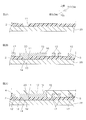
- FIGS. 3D to 3E are process drawings for explaining the method of manufacturing the printed circuit board shown in FIG. 1B following FIG. 2C, and FIG.
- FIG. 3D is a third step of providing a shield layer
- FIG. 3E is a cover insulating layer. It shows the process of providing.
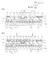
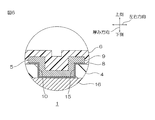
- FIG. 4 shows a modification of the printed circuit board shown in FIG. 1B.
- FIG. 5 shows a modification of the printed circuit board shown in FIG. 1B.
- FIG. 6 shows a modification of the printed circuit board shown in the enlarged view of FIG. 1B.
- the left-right direction in the drawing shows the left-right direction (first direction).
- the vertical direction of the drawing shows the vertical direction (an example of the thickness direction) (second direction orthogonal to the first direction)
- the upper side of the drawing is the upper side (an example of one side in the thickness direction) (second direction one side)
- the lower side of the drawing shows the lower side (the other side in the thickness direction) (the other side in the second direction).
- the up and down direction on the drawing indicates the front-rear direction (a third direction orthogonal to the first direction and the second direction).
- the direction conforms to the direction arrow in each figure.
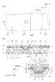
- the cover insulating layer 6 (described later) is omitted to clearly show the arrangement and shape of the shield layer 5 (described later).
- the printed circuit board 1 has a sheet shape having a predetermined thickness T and extending in the surface direction (both in the left-right direction and in the front-rear direction).
- the wired circuit board 1 is a wired circuit board for an imaging device to be electrically connected to an imaging element (not shown) disposed on the lower side and provided (embedded) in an imaging device (not shown). is there.
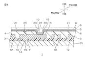
- the printed circuit board 1 includes a base insulating layer 2, a conductor layer 3, an intermediate insulating layer 4 as an example of an insulating layer, a shield layer 5, and a cover insulating layer 6 in order from the upper side.
- the base insulating layer 2 has a sheet shape extending in the surface direction.
- the base insulating layer 2 forms the lower surface of the printed circuit board 1.
- the base insulating layer 2 has a base opening 11 penetrating in the thickness direction.
- the material of the base insulating layer 2 is an insulating material.
- the insulating material include synthetic resins such as polyimide, polyamide imide, acrylic, polyether nitrile, polyether sulfone, polyethylene terephthalate, polyethylene naphthalate, polyvinyl chloride and the like.
- a polyimide etc. are mentioned.
- the thermal expansion coefficient of the base insulating layer 2 is, for example, 10 (ppm / K) or more, preferably 15 (ppm / K) or more, and for example, 50 (ppm / K) or less.
- the thermal expansion coefficient of the base insulating layer 2 is a linear thermal expansion coefficient in the surface direction, and can be measured, for example, by thermal mechanical analysis under the conditions of JIS K7197.
- the thickness of the base insulating layer 2 is, for example, 1 ⁇ m or more, preferably 5 ⁇ m or more, and for example, 30 ⁇ m or less, preferably 10 ⁇ m or less.
- the conductor layer 3 is disposed on the base insulating layer 2.
- the conductor layer 3 has a plurality of patterns spaced apart from one another in the surface direction.
- the conductor layer 3 independently includes a signal layer 12 electrically connected to an imaging element (not shown) and a ground layer 13.
- a plurality of signal layers 12 are arranged on the upper surface of the base insulating layer 2 at intervals in the surface direction.
- the signal layer 12 is electrically connected to an imaging device (described later, not shown).
- the ground layer 13 integrally includes a ground contact portion 14 and an extension portion 16 extending in the surface direction from the ground contact portion 14.
- the ground contact portion 14 is positioned in the base opening 11 when projected in the thickness direction, and extends in the vertical direction.
- the ground contact portion 14 includes a ground lower portion 19 filled in the base opening 11 and a ground upper portion 20 continuously provided on the upper side of the ground lower portion 19.
- the extension portion 16 is integrally formed with the upper ground portion 20.
- the extension portion 16 is disposed adjacent to the ground contact portion 14 when projected in the thickness direction.
- the material of the conductor layer 3 examples include metal materials such as copper, silver, gold, nickel or alloys containing them, and solder. Preferably, copper is mentioned.
- the thickness of the conductor layer 3 is 1 ⁇ m or more, preferably 3 ⁇ m or more, and for example, 15 ⁇ m or less, preferably 10 ⁇ m or less.
- the intermediate insulating layer 4 has a sheet shape extending in the surface direction.
- the intermediate insulating layer 4 is disposed on the upper surface of the base insulating layer 2 so as to cover the conductor layer 3. Specifically, the intermediate insulating layer 4 covers the signal layer 12, the ground upper portion 20 and the extension portion 16.
- the intermediate insulating layer 4 has an intermediate opening 15 as an example of an insulating opening that exposes the upper surface of a part of the extension 16.
- the intermediate opening 15 penetrates the intermediate insulating layer 4 (in the upper portion with respect to the extending portion 16) in the thickness direction.
- the intermediate opening 15 has a tapered shape in which the opening cross-sectional area (opening cross-sectional area when cut along the surface direction) becomes smaller toward the lower side.
- the inner side surface 10 of the intermediate insulating layer 4 partitioning the intermediate opening 15 has a cylindrical shape extending along the thickness direction, and more specifically, when cut along the thickness direction and the left and right direction ), Which are tapered surfaces (inclined surfaces) opposed to each other in the left-right direction, and the opposing distances thereof become smaller toward the lower side. That is, the intermediate opening 15 has a substantially frusto-conical shape whose diameter decreases downward.
- the material of the intermediate insulating layer 4 is the same as the material of the base insulating layer 2.
- the thickness of the intermediate insulating layer 4 is a distance between the upper surface of the base insulating layer 2 and the upper surface of the intermediate insulating layer 4 and is, for example, 1 ⁇ m or more, preferably 5 ⁇ m or more, and for example, 30 ⁇ m or less, preferably Is 10 ⁇ m or less.
- the maximum length (maximum diameter) of the upper end edge of the intermediate opening 15 is, for example, 10 ⁇ m or more, preferably 50 ⁇ m or more, and for example, 2000 ⁇ m or less, preferably 1500 ⁇ m or less.
- the maximum length (maximum diameter) of the lower end edge of the intermediate opening 15 is, for example, 10 ⁇ m or more, preferably 50 ⁇ m or more, and for example, 2000 ⁇ m or less, preferably 1500 ⁇ m or less.
- An angle ⁇ between the inner side surface 10 and the upper surface of the extension 16 exposed from the intermediate opening 15 is, for example, 90 degrees or more, preferably 120 degrees or more, and for example, 170 degrees or less, preferably , Less than 160 degrees.
- the shield layer 5 is a layer that shields electromagnetic waves from the outside.
- the shield layer 5 is disposed on the upper side with respect to the conductor layer 3.
- the shield layer 5 has a sheet shape extending in the front-rear direction. Specifically, a plurality of shield layers 5 are arranged at intervals in the left-right direction. Thus, shield openings 27 are provided between the adjacent shield layers 5.
- a plurality of shield openings 27 are provided at intervals in the left-right direction, and each shield opening 27 exposes the upper surface of a part of the intermediate insulating layer 4. Further, the shield layer 5 is provided with the above-described shield opening 27 and has a pattern including the intermediate opening 15.
- the area ratio of the shield opening 27 in the shield layer 5 is, for example, 1% or more, preferably 10% or more, and for example, 90% or less, preferably 70% or less.
- the shield layer 5 includes a flat portion 21 and a recess 22.
- the flat portion 21 is disposed on the upper surface of the intermediate insulating layer 4.
- the flat portion 21 also has a pattern surrounding the intermediate opening 15.
- the flat portion 21 has a predetermined thickness and has a sheet shape extending in the surface direction.
- the recess 22 is disposed in the middle opening 15 and has a shape that is recessed downward from the inner edge of the flat portion 21 around the middle opening 15.
- the recess 22 has a substantially U-shaped cross section which is disposed continuously with the inner surface 10 and the upper surface of the extension 16 exposed from the intermediate opening 15.
- the recess 22 integrally includes the side wall 23 and the second flat portion 24.
- the side wall 23 is an inclined wall which is inclined downward (specifically, obliquely downward and inward) from the inner edge of the recess 22 around the middle opening 15.
- the side wall 23 has a substantially truncated cone shape (a truncated cone whose inside is hollow) whose diameter decreases downward.
- the side wall 23 covers the inner surface 10.
- the second flat portion 24 is a bottom wall connecting the lower end edge of the side wall 23.
- the second flat portion 24 is in contact with the upper surface of the extension 16 exposed from the intermediate opening 15.
- the second flat portion 24 has a shape corresponding to the lower end edge of the inner side surface 10, specifically, a substantially circular shape in plan view.
- the thickness of the flat portion 21, the thickness of the side wall 23, and the thickness of the second flat portion 24 are substantially the same, which is the thickness Ts of the shield layer 5.
- the shield layer 5 includes the adhesion layer 8 and the main body layer 9 in order from the upper side.
- the shield layer 5 is a laminate of the adhesion layer 8 and the main body layer 9.
- the shield layer 5 comprises only the adhesion layer 8 and the main body layer 9.
- each of the flat portion 21 and the recess 22 includes the adhesion layer 8 and the main body layer 9.
- the main body layer 9 adheres to the upper surface of the intermediate insulating layer 4 via the adhesive layer 8.
- the main body layer 9 is in close contact with the inner side surface 10 of the intermediate insulating layer 4 via the adhesion layer 8 and in close contact with the upper surface of the extension 16 exposed from the intermediate opening 15.
- the adhesion of the adhesion layer 8 to the intermediate insulation layer 4 and the adhesion of the adhesion layer 8 to the main layer 9 are larger than the adhesion of the main layer 9 to the intermediate insulation layer 4.
- chromium, nickel, etc. are mentioned, for example, Preferably, chromium is mentioned. If the material of the adhesion layer 8 is chromium, the adhesion of the main body layer 9 to the intermediate insulating layer 4 and the adhesion of the main body layer 9 to the extension 16 exposed from the intermediate opening 15 are further enhanced. Can.
- the thermal expansion coefficient of the adhesion layer 8 is different from, for example, the thermal expansion coefficient of the intermediate insulating layer 4. Specifically, the thermal expansion coefficient of the adhesion layer 8 is smaller than the thermal expansion coefficient of the intermediate insulating layer 4, and more specifically, for example, 90% of the thermal expansion coefficient of the intermediate insulating layer 4
- the content is preferably 75% or less, more preferably 50% or less, and even more preferably 45% or less, and for example, 10% or more, preferably 20% or more.
- the adhesive layer 8 stretches in the surface direction of the intermediate insulating layer 4 by heating in the manufacturing process described later. It is difficult to follow, and the crack in the adhesion layer 8 is likely to be damaged.
- the ratio (Tb / Ta) of the thickness Tb of the main body layer 9 to the thickness Ta of the adhesion layer 8 is 4 or more. 8 damage can be suppressed.
- the thermal expansion coefficient of the adhesion layer 8 is, for example, less than 10 (ppm / K), preferably 9 (ppm / K) or less, more preferably 8 (ppm / K) or less, For example, it is 1 (ppm / K) or more.
- the thickness Ta of the adhesion layer 8 is set to satisfy a ratio (Tb / Ta) described later to the thickness Ta of the adhesion layer 8 of the thickness Tb of the main body layer 9, and specifically, for example, less than 100 nm, preferably 50 nm or less, more preferably 40 nm or less, still more preferably 30 nm or less, and for example, 2 nm or more.
- the material of the main body layer 9 is selected so that the adhesion of the adhesion layer 8 to the main body layer 9 is larger than the adhesion of the main body layer 9 to the intermediate insulating layer 4.
- the material of the main body layer 9 may be, for example, the same as or different from the material of the adhesion layer 8, and preferably different.
- examples of the material of the main body layer 9 include metals such as copper, chromium, nickel, gold, silver, platinum, palladium, titanium, tantalum, solder, or alloys thereof, preferably copper, Nickel, more preferably copper.
- the thermal expansion coefficient of the main body layer 9 approximates, for example, the thermal expansion coefficient of the intermediate insulating layer 4.
- the thermal expansion coefficient of the main body layer 9 is, for example, 70% or more, preferably 80% or more, more preferably 90% or more, preferably 95% or more, relative to the thermal expansion coefficient of the intermediate insulating layer 4 Also, for example, it is 110% or less, preferably 100% or less.
- the thermal expansion coefficient of the main layer 9 is the thermal expansion coefficient of the intermediate insulating layer 4 Similar to the above, even if the thermal expansion coefficient of the adhesive layer 8 is significantly different from the thermal expansion coefficient of the intermediate insulating layer 4, the elongation of the intermediate insulating layer 4 and the elongation of the adhesive layer 8 in heating in the manufacturing process described later It can be made to match and damage to adhesion layer 8 can be controlled.
- the thermal expansion coefficient of the main layer 9 is, for example, 10 (ppm / K) or more, preferably 13 (ppm / K) or more, more preferably 15 (ppm / K) or more, For example, it is 20 (ppm / K) or less.
- the thickness Tb of the main body layer 9 is set to satisfy a ratio (Tb / Ta) described later, and specifically, for example, 50 nm or more, preferably 100 nm or more, more preferably 110 nm or more, For example, it is 250 nm or less, preferably 200 nm or less.
- the ratio (Tb / Ta) of the thickness Tb of the main body layer 9 to the thickness Ta of the adhesion layer 8 is 4 or more, preferably 5 or more, and for example, 20 or less, preferably 10 or less.
- the ratio (Tb / Ta) is less than the above-described lower limit, the adhesion of the shield layer 5 can not be improved.
- the ratio (Tb / Ta) is equal to or more than the above-described lower limit, so that the adhesion of the shield layer 5 can be improved.
- ratio (Tb / Ta) is more than the above-mentioned lower limit, adhesion layer 8 will be thin enough compared with body layer 9. Therefore, the adhesion layer 8 can follow the intermediate insulating layer 4 and the main body layer 9, and the damage in the adhesion layer 8 can be suppressed. Further, when the ratio (Tb / Ta) is equal to or more than the above-described lower limit, the main body layer 9 is sufficiently thicker than the adhesion layer 8. Therefore, the main body layer 9 can sufficiently press the adhesion layer 8, so that damage in the adhesion layer 8 can be suppressed.
- the thickness Ts of the shield layer 5 is, for example, 60 nm or more, preferably 100 nm or more, and for example, 3000 nm or less, preferably 1000 nm or less.
- the thickness Ts of the shield layer 5 is the sum (Ta + Tb) of the thickness Ta of the adhesion layer 8 and the thickness Tb of the main body layer 9.
- the cover insulating layer 6 has a sheet shape extending in the surface direction.
- the cover insulating layer 6 forms the upper surface of the printed circuit board 1.
- the cover insulating layer 6 is disposed on the upper surface of the intermediate insulating layer 4 so as to cover the shield layer 5.
- the cover insulating layer 6 is also filled in the recess 22.
- the cover insulating layer 6 is the same as the material of the base insulating layer 2.
- the thermal expansion coefficient of the cover insulating layer 6 is the same as the thermal expansion coefficient of the base insulating layer 2.
- the thickness of the cover insulating layer 6 is not particularly limited, and is, for example, 1 ⁇ m or more, preferably 5 ⁇ m or more, and for example, 30 ⁇ m or less, preferably 10 ⁇ m or less.
- the thickness T of the printed circuit board 1 is the sum of the thicknesses of the base insulating layer 2, the intermediate insulating layer 4 and the cover insulating layer 6. Specifically, the lower surface of the base insulating layer 2 and the upper surface of the cover insulating layer 6 Distance. Specifically, the thickness T of the printed circuit board 1 is, for example, 5 ⁇ m or more, preferably 10 ⁇ m or more, and for example, 100 ⁇ m or less, preferably 50 ⁇ m or less.
- the steps of providing the base insulating layer 2 on the support substrate 25, the first step of providing the conductor layer 3, and the intermediate insulating layer 4 A second step of providing, a third step of providing the shield layer 5, a step of providing the cover insulating layer 6, and a step of removing the support substrate 25 are sequentially provided.
- the support substrate 25 is prepared.
- the support substrate 25 has a sheet shape extending in the surface direction and having a flat upper surface.
- Examples of the material of the support substrate 25 include metals such as stainless steel, 42 alloy, and aluminum, for example, resins, for example, ceramics, and the like, with preference given to metals.
- the thickness of the support substrate 25 is, for example, 5 ⁇ m or more, preferably 10 ⁇ m or more, and for example, 50 ⁇ m or less, preferably 30 ⁇ m or less.
- the base insulating layer 2 having the base opening 11 is formed on the upper surface of the support substrate 25 from an insulating material by photo processing, for example.
- the base insulating layer 2 in which the base opening 11 is formed is disposed (placed) on the upper surface of the support substrate 25 in advance.
- the insulating base layer 2 is provided on the upper surface of the support substrate 25.
- the conductor layer 3 is provided on the base insulating layer 2.
- the conductor layer 3 is formed from the signal layer 12 and the ground layer 13 by a patterning method such as, for example, an additive method or a subtractive method.
- the intermediate insulating layer 4 covers the conductor layer 3 and has an intermediate opening 15 that exposes the upper surface of a part of the extension 16. Set up.
- an intermediate insulating layer 4 having an intermediate opening 15 is formed from the insulating material on the entire top surface of the base insulating layer 2 and the top and side surfaces of the conductor layer 3 by photo processing.
- the intermediate insulating layer 4 in which the intermediate opening 15 is formed is arranged (mounted) in advance on the base insulating layer 2 and the conductor layer 3.
- the intermediate insulating layer 4 is provided so as to cover the conductor layer 3 (excluding a part of the extension 16) and to have the intermediate opening 15.
- the shield layer 5 is provided on the upper surface of the intermediate insulating layer 4 so as to have a recess 22 which is disposed in the intermediate opening 15 and is recessed downward.
- the adhesion layer 8 is formed by a thin film forming method such as sputtering or plating (electroless plating) (fourth step), and then the main body layer 9 is formed (fifth step)
- the shield layer 5 is formed from the adhesion layer 8 and the main body layer 9.
- the shield layer 5 is formed by sputtering. In the case of sputtering, it is possible to form a shield layer 5 of uniform thickness (specifically, an adhesion layer 8 of uniform thickness and a body layer 9 of uniform thickness).
- the method of forming the adhesion layer 8 and the method of forming the main body layer 9 may be the same as or different from each other, and are preferably the same.
- each of the adhesion layer 8 and the main body layer 9 is formed by sputtering. That is, the adhesion layer 8 is formed by sputtering (fourth step), and subsequently, the main body layer 9 is formed by sputtering on the upper surface of the adhesion layer 8 (fifth step).
- the shield opening 27 is formed in the shield layer 5 by, for example, a thin film removal method such as etching (dry etching, wet etching).
- the cover insulating layer 6 is provided on the upper surface of the intermediate insulating layer 4 and the upper surface and the side surface of the shield layer 5.
- the cover insulating layer 6 is provided by photo processing. Specifically, in photo processing, first, a photosensitive insulating composition containing a photosensitive component and an insulating material is prepared, and then, the photosensitive insulating composition is formed on the upper surface of the intermediate insulating layer 4 and the upper surface of the shield layer 5 Apply to the side and then dry if necessary to form a film. Then, the film is exposed through a photomask and developed to form a cover insulating layer 6. Thereafter, the cover insulating layer 6 is heated (heating after exposure).
- the heating conditions are, for example, conditions under which the insulating material can be sufficiently cured (specifically, imidization and the like). Specifically, the temperature is, for example, 250 ° C. or more, preferably 300 ° C. or more, Also, for example, the temperature is 400 ° C. or less, and the time is, for example, 10 minutes or more, preferably 30 minutes or more, and for example, 100 minutes or less.
- the cover insulating layer 6 formed in a predetermined pattern in advance is disposed (placed) on the intermediate insulating layer 4 and the shield layer 5.
- photo processing is used from the viewpoint of reliable patterning and arrangement.
- the support substrate 25 is then removed from the lower surface of the insulating base layer 2 and the lower surface of the lower ground portion 19 by, for example, peeling.
- the lower surface of the base insulating layer 2 and the lower surface of the lower ground portion 19 are exposed to the lower side.
- an imaging element (not shown) is prepared under the printed circuit board 1, and the imaging element (not shown) is electrically connected to the signal layer 12. Further, the ground contact portion 14 is electrically connected to a ground contact (not shown) to ground the ground layer 13.
- the imaging device 30 provided with the printed circuit board 1 and an imaging element (not shown) is obtained.
- shield layer 5 has crevice 22, and even if stress F shown in arrow F of Drawing 1B is applied to shield layer 5 and it is going to expand and contract, shield layer 5 is an adhesion layer. 8, and the ratio (Tb / Ta) of the thickness Tb of the main body layer 9 to the thickness Ta of the adhesion layer 8 is 4 or more, so that the intermediate insulating layer 4 is provided. It is possible to suppress the decrease in the adhesion to the surface, and to suppress the decrease in the adhesion to a part of the extension portion 16.
- the shield opening 27 is provided in a portion where the shielding of the electromagnetic wave is unnecessary, and the electromagnetic wave is shielded by the shield layer 5 in other portions. can do.
- the main body layer 9 is formed of the adhesion layer 8. The reduction in adhesion to the intermediate insulating layer 4 can be more effectively suppressed.
- the printed circuit board 1 is a printed circuit board for an imaging device, the imaging device 30 excellent in reliability can be manufactured.
- the adhesion layer 8 and the intermediate insulating layer 4 have different coefficients of thermal expansion, heating of the cover insulating layer 6 shown in FIG. 3E (heating after exposure) As a result, due to the difference in thermal expansion coefficient between the adhesion layer 8 and the intermediate insulating layer 4, the adhesion layer 8 is likely to be damaged such as a crack.
- the ratio (Tb / Ta) of the thickness Tb of the main body layer 9 to the thickness Ta of the adhesive layer 8 is 4 or more. Damage can be suppressed.
- the thermal expansion coefficient (17 (ppm / K)) of polyimide is similar to the thermal expansion coefficient (16.8 (ppm / K)) of copper, the thermal expansion coefficient of chromium (6.8 (ppm / K) It differs significantly from)). Therefore, the adhesion layer 8 can not follow the elongation of the intermediate insulation layer 4 and the main body layer 9 by heating (heating after exposure) of the cover insulating layer 6 shown in FIG. 3E, and damage such as cracks occurs in the adhesion layer 8 easy.
- the imaging device 30 which is excellent in reliability can be manufactured.
- the printed circuit board 1 has been described as a printed circuit board for an imaging device, but the application is not limited to this, and for example, a test board (anisotropic conductive sheet), a flexible printed circuit board, etc. It can be used.
- middle opening part 15 exposes the upper surface of a part of the extension part 16, although it does not show in figure, for example, it replaces with this or
- the upper surface of (the part or all of) the upper ground portion 20 can be exposed.
- the second flat portion 24 of the recess 22 contacts the upper surface of the upper ground portion 20.
- the shield opening 27 is formed in the shield layer 5.
- the shield layer 5 not having the shield opening 27 may be formed from the entire upper surface of the intermediate insulating layer 4, the inner side surface 10 and the intermediate opening 15. It can also be continuously formed on the exposed upper surface of the extending portion 16.
- a shield opening 27 is formed in the shield layer 5.
- the shield opening 27 is not formed in the shield layer 5
- the gas from the intermediate insulating layer 4 water vapor derived from the moisture absorbed by the intermediate insulating layer 4 is obtained by heating in the step shown in FIG. Even if G) is generated, the shield layer 5 shields the gas G, which causes damage such as deformation of the intermediate insulating layer 4, and as a result, the adhesion of the adhesive layer 8 to the intermediate insulating layer 4 descend.
- the gas G described above can be efficiently released from the shield opening 27. Therefore, the adhesion of the shield layer 5 to the intermediate insulating layer 4 can be further improved.
- the shield layer 5 can be configured without providing the recess 22.
- the shield layer 5 continuously has the flat portion 21 and the filling portion 28 with which the intermediate opening 15 is filled, and their upper surface has a flat shape.
- the upper surface of the shield layer 5 is parallel to the upper surface of the intermediate insulating layer 4.
- the filling portion 28 is solid and has a flat upper surface.
- the inner surface 10 has a tapered shape, but may have a straight shape along the thickness direction, for example, as shown in FIG.
- blending ratios content ratios
- physical property values parameters, etc. used in the following description are the blending ratios (content ratios) corresponding to those described in the above-mentioned “embodiments for carrying out the invention” ), Physical property values, parameters, etc. may be substituted for the upper limit (numerical values defined as “below”, “less than”) or lower limit (numerical values defined as “above”, “exceed”), etc. it can.
- Example 1 As shown in FIG. 2A, the base insulating layer 2 made of polyimide was formed by photo processing on the upper surface of the support substrate 25 made of stainless steel.
- a conductor layer 3 comprising a signal layer 12 and a ground layer 13 independently and made of copper was formed on the upper surface of the base insulating layer 2 by an additive method (first step).
- an intermediate insulating layer 4 having an intermediate opening 15 and made of polyimide (coefficient of thermal expansion 17 (ppm / K)) is coated with the conductor layer 3 on the upper surface of the base insulating layer 2. As a result, it was formed by photo processing (second step).
- the thickness of the intermediate insulating layer 4 was 10 ⁇ m.
- the adhesion layer 8 is formed of chromium (thermal expansion coefficient 6.8 (ppm / K)) and has a thickness Ta of 30 ⁇ m by sputtering (fourth step)
- a main body layer 9 made of copper (thermal expansion coefficient 16.8 (ppm / K)) and having a thickness Tb of 120 ⁇ m was formed by a sputtering method (fifth step).
- the shield layer 5 having the flat portion 21 and the concave portion 22 was formed.
- Shield layer 5 does not have shield opening 27 yet, that is, adhesion layer 8 is formed from the entire upper surface of intermediate insulating layer 4, inner side surface 10 of shield layer 5, and intermediate opening 15. It formed continuously with the upper surface of the extension part 16 to expose, and formed the main layer 9 in the whole upper surface of the contact
- the shield layer 5 was formed into a pattern having the shield opening 27 by wet etching (third step).
- a cover insulating layer 6 was formed on the upper surface of the intermediate insulating layer 4 so as to cover the shield layer 5 by photo processing. Specifically, a photosensitive polyimide composition is applied to the upper surface of the intermediate insulating layer 4 and the upper and side surfaces of the shield layer 5 and then dried to form a film, and then through a photomask. The film was exposed and developed to form a cover insulating layer 6. Thereafter, the cover insulating layer 6 was post-exposure heated at 325 ° C. for 20 minutes.
- the support substrate 25 was removed by peeling.
- the printed circuit board 1 was manufactured.
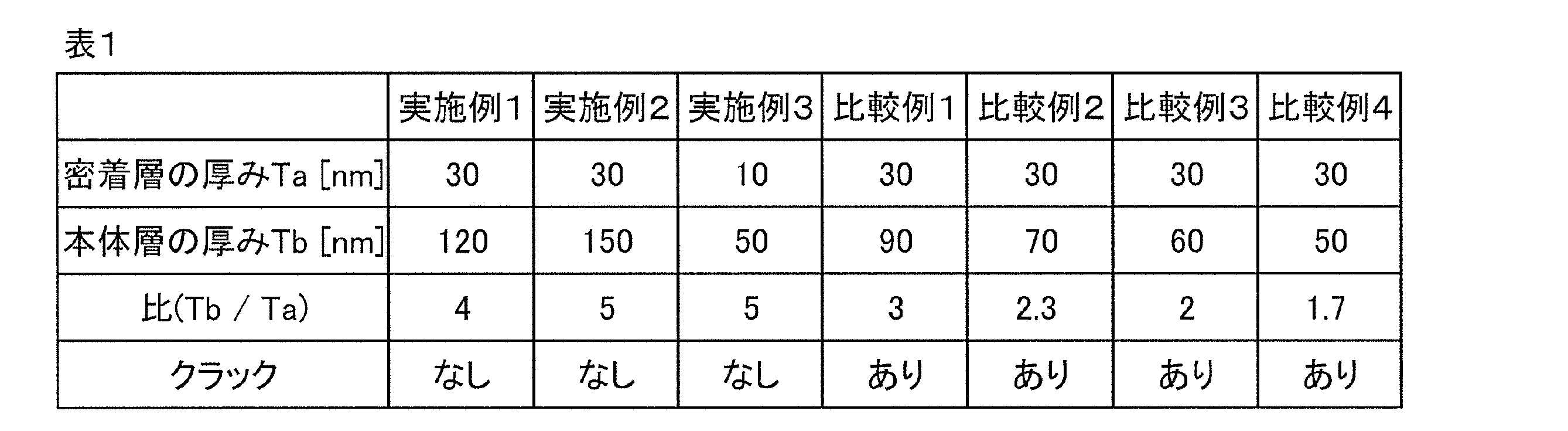
- Example 2 to Comparative Example 2 A printed circuit board 1 was manufactured in the same manner as in Example 1 except that the thickness Ta of the adhesion layer 8 and the thickness Tb of the main body layer 9 were changed according to Table 1.
- the wired circuit board is used for an imaging device.
- Wiring circuit board (wiring circuit board for imaging device) Reference Signs List 3 conductor layer 4 intermediate insulating layer 5 shield layer 8 adhesion layer 9 main body layer 15 intermediate opening 22 concave portion 30 thickness of imaging device Ta adhesion layer thickness of Tb main body layer
Landscapes
- Engineering & Computer Science (AREA)
- Microelectronics & Electronic Packaging (AREA)
- Manufacturing & Machinery (AREA)
- Physics & Mathematics (AREA)
- Electromagnetism (AREA)
- Chemical & Material Sciences (AREA)
- Inorganic Chemistry (AREA)
- Shielding Devices Or Components To Electric Or Magnetic Fields (AREA)
- Structure Of Printed Boards (AREA)
- Production Of Multi-Layered Print Wiring Board (AREA)
- Laminated Bodies (AREA)
Abstract
配線回路基板は、導体層と、絶縁層と、シールド層とを厚み方向一方側に向かって順に備える。絶縁層は、導体層を被覆しており、導体層の一部の前記厚み方向一方面を露出する絶縁開口部を有し、シールド層は、絶縁開口部内に配置され、導体層に接触するように、厚み方向他方側に向かって凹む凹部を有する。シールド層は、密着層と、本体層とを厚み方向一方側に向かって順に備える。密着層の厚みTaに対する本体層の厚みTbの比(Tb/Ta)が、4以上である。
Description
本発明は、配線回路基板およびその製造方法に関する。
従来、グランド層と、絶縁層とを備える配線回路基板が知られている(例えば、特許文献1参照。)。
特許文献1では、グランド層は、下部グランド層と、絶縁層の開口部に充填され、下部グランド層に接触する側部グランド配線と、絶縁層の上面に配置され、側部グランド配線と一体的に形成される上部グランド配線とを備える。上部グランド層は、側部グランド配線を介して下部グランド配線と電気的に接続されており、シールド層として作用している。
特許文献1では、側部グランド配線および上部グランド配線は、断面略T字形状を有しており、上部グランド配線の上面は、平坦形状を有する。そのため、グランド層は、優れた強度を有し、グランド層に応力が付与されても、形状維持性に優れる。従って、グランド層の絶縁層に対する密着性が低下しにくい。
一方、配線回路基板の用途および目的によっては、上部グランド配線の上面が、絶縁層の開口部に対応して下側に向かって凹む凹部を有する場合がある。その場合には、凹部に起因して、グランド層の強度が低く、そのため、グランド層に応力がかかると、上部グランド配線が面方向に伸縮し易く、そのため、上部グランド配線の絶縁層に対する密着性、さらには、側部グランド配線の下部グランド配線に対する密着性も低下するという不具合がある。
そこで、本願発明者は、シールド層が凹部を有していても、シールド層の密着性が向上された配線回路基板を鋭意検討したところ、シールド層が、密着層と、本体層とを備え、さらに、密着層の厚みTaに対する本体層の厚みTbの比(Tb/Ta)が、4以上であれば、シールド層の密着性を向上させることができるという知見を見出した。
本発明(1)は、導体層と、絶縁層と、シールド層とを厚み方向一方側に向かって順に備え、前記絶縁層は、前記導体層を被覆しており、前記導体層の一部の前記厚み方向一方面を露出する絶縁開口部を有し、前記シールド層は、前記絶縁開口部内に配置され、前記導体層に接触するように、前記厚み方向他方側に向かって凹む凹部を有し、前記シールド層は、密着層と、本体層とを前記厚み方向一方側に向かって順に備え、前記密着層の厚みTaに対する前記本体層の厚みTbの比(Tb/Ta)が、4以上である、配線回路基板を含む。
この配線回路基板では、シールド層は、凹部を有し、シールド層に応力がかかり、伸縮しても、シールド層は、密着層と、本体層とを厚み方向一方側に向かって順に備え、密着層の厚みTaに対する本体層の厚みTbの比(Tb/Ta)が、4以上であるので、絶縁層に対する密着性の低下を抑制でき、さらには、導体層の一部に対する密着性の低下を抑制することができる。
本発明(2)は、前記シールド層は、前記絶縁層の一部の前記厚み方向一方面を露出するシールド開口部を有する、(1)に記載の配線回路基板を含む。
また、この配線回路基板では、シールド層がシールド開口部を有するので、電磁波の遮蔽を不要とする部分にシールド開口部を設け、それ以外の部分において、シールド層によって電磁波を遮蔽することができる。
本発明(3)は、前記絶縁層の材料が、ポリイミドであり、前記密着層の材料が、クロムであり、前記本体層の材料が、銅である、(1)または(2)に記載の配線回路基板を含む。
この配線回路基板では、密着層により、本体層の絶縁層に対する密着性の低下をより一層有効に抑制することができる。
本発明(4)は、撮像装置用配線回路基板である、(1)~(3)のいずれか一項に記載の配線回路基板を含む。
この配線回路基板は、撮像装置用配線回路基板であるので、信頼性に優れる撮像装置を製造することができる。
本発明(5)は、導体層と、絶縁層と、シールド層とを厚み方向一方側に向かって順に備え、前記シールド層は、前記絶縁層の一部の前記厚み方向一方面を露出するシールド開口部を有する、配線回路基板を含む。
また、この配線回路基板では、シールド層がシールド開口部を有するので、電磁波の遮蔽を不要とする部分にシールド開口部を設け、それ以外の部分において、シールド層によって電磁波を遮蔽することができる。
本発明(6)は、導体層を設ける第1工程と、絶縁層を、前記導体層を被覆し、かつ、前記導体層の一部の前記厚み方向一方面を露出する絶縁開口部を有するように、設ける第2工程と、シールド層を、前記絶縁開口部内に配置され、前記厚み方向他方側に向かって凹む凹部を有するように、前記絶縁層の前記厚み方向一面に設ける第3工程とを備え、前記第3工程は、密着層を、前記絶縁層の前記厚み方向一方面、前記絶縁開口部に臨む前記絶縁層の内側面、および、前記絶縁開口部から露出する前記導体層の前記厚み方向一方面に設ける第4工程と、本体層を、前記密着層の前記厚み方向一方面に設ける第5工程とを備え、前記密着層の厚みTaに対する前記本体層の厚みTbの比(Tb/Ta)が、4以上である、配線回路基板の製造方法を含む。
この配線回路基板の製造方法では、シールド層は、凹部を有し、シールド層に応力がかかり、伸縮しても、シールド層は、密着層と、本体層とを厚み方向一方側に向かって順に備え、密着層の厚みTaに対する本体層の厚みTbの比(Tb/Ta)が、4以上であるので、絶縁層に対する密着性の低下を抑制でき、さらには、導体層の一部に対する密着性の低下を抑制することができる。
また、密着層と、絶縁層とは、熱膨張率が相違する場合には、その後の工程の加熱によって、それらの熱膨張率の相違に起因して、密着層にクラックなどの損傷を生じ易い。
しかし、この配線回路基板の製造方法では、密着層の厚みTaに対する本体層の厚みTbの比(Tb/Ta)が、4以上であるので、熱膨張率の相違に起因する上記した損傷を抑制することができる。
本発明(7)は、前記第3工程では、前記シールド層に、前記絶縁層の一部の前記厚み方向一方面を露出するシールド開口部を設ける、(6)に記載の配線回路基板の製造方法を含む。
この製造方法によれば、その後の工程の加熱によって、絶縁層からガスが発生しても、かかるガスを効率よくシールド開口部から放出することができる。そのため、シールド層の絶縁層に対する密着性をより一層向上させることができる。
本発明(8)は、前記第2工程において、前記絶縁層を、ポリイミドから形成し、前記第4工程において、前記密着層を、クロムから形成し、前記第5工程において、前記本体層を、銅から形成する、(6)または(7)に記載の配線回路基板の製造方法を含む。
この配線回路基板の製造方法では、密着層により、本体層の絶縁層に対する密着性の低下をより一層有効に抑制することができる。
また、ポリイミドの熱膨張係数は、銅の熱膨張係数に類似する一方、クロムの熱膨張係数と顕著に相違する。そのため、密着層が、その後の工程の加熱によって、絶縁層および本体層の伸びに追従できず、密着層にクラックなどの損傷を生じ易い。
しかし、この製造方法によれば、密着層の厚みTaに対する本体層の厚みTbの比(Tb/Ta)が、4以上であるので、シールド層の絶縁層に対する良好な密着性を確保することができる。
本発明(9)は、撮像装置用配線回路基板の製造方法である、(6)~(8)のいずれか一項に記載の配線回路基板の製造方法を含む。
この製造方法は、撮像装置用配線回路基板の製造方法であるので、得られた配線回路基板から、信頼性に優れる撮像装置を製造することができる。
本発明(10)は、導体層を設ける第1工程と、絶縁層を前記導体層を被覆するように設ける第2工程と、シールド層を前記絶縁層の前記厚み方向一面に設ける第3工程とを備え、前記第3工程では、前記シールド層に、前記絶縁層の一部の前記厚み方向一方面を露出するシールド開口部を設ける、配線回路基板の製造方法を含む。
この配線回路基板の製造方法では、シールド層がシールド開口部を有するので、電磁波の遮蔽を不要とする部分にシールド開口部を設けることができる。
さらに、この製造方法によれば、その後の工程の加熱によって、絶縁層からガスが発生しても、かかるガスを効率よくシールド開口部から放出することができる。そのため、シールド層の絶縁層に対する密着性をより一層向上させることができる。
本発明の配線回路基板およびその製造方法では、絶縁層に対する密着性の低下を抑制できる。
本発明の配線回路基板およびその製造方法では、電磁波の遮蔽を不要とする部分にシールド開口部を設けることができる。
[配線回路基板およびその製造方法の一実施形態]
図1Aおよび図1Bにおいて、紙面左右方向は、左右方向(第1方向)を示す。図1Bにおいて、紙面上下方向は、上下方向(厚み方向の一例)(第1方向に直交する第2方向)を示し、紙面上側が上側(厚み方向一方側の一例)(第2方向一方側)、紙面下側が下側(厚み方向他方側)(第2方向他方側)を示す。図1Aにおいて、紙面上下方向は、前後方向(第1方向および第2方向に直交する第3方向)を示す。
図1Aおよび図1Bにおいて、紙面左右方向は、左右方向(第1方向)を示す。図1Bにおいて、紙面上下方向は、上下方向(厚み方向の一例)(第1方向に直交する第2方向)を示し、紙面上側が上側(厚み方向一方側の一例)(第2方向一方側)、紙面下側が下側(厚み方向他方側)(第2方向他方側)を示す。図1Aにおいて、紙面上下方向は、前後方向(第1方向および第2方向に直交する第3方向)を示す。
具体的には、方向は、各図の方向矢印に準拠する。
これらの方向の定義により、配線回路基板1および撮像装置30(後述)の製造時および使用時の向きを限定する意図はない。
なお、図1Aにおいて、カバー絶縁層6(後述)は、シールド層5(後述)の配置および形状を明確に示すために、省略している。
また、以降の各図は、各部材の角度、寸法などが、本願発明を容易に理解するために誇張して描画されており、正確に表されていない場合を含む。
図1Aおよび図1Bに示すように、配線回路基板1は、所定の厚みTを有し、面方向(左右方向および前後方向の両方)に延びるシート形状を有する。配線回路基板1は、下側に配置される撮像素子(図示せず)と電気的に接続されて、撮像装置(図示せず)に備えられる(組み込まれる)ための撮像装置用配線回路基板である。
配線回路基板1は、ベース絶縁層2と、導体層3と、絶縁層の一例としての中間絶縁層4と、シールド層5と、カバー絶縁層6とを上側に向かって順に備える。
ベース絶縁層2は、面方向に延びるシート形状を有する。ベース絶縁層2は、配線回路基板1の下面を形成する。ベース絶縁層2は、厚み方向を貫通するベース開口部11を有する。
ベース絶縁層2の材料は、絶縁材料である。絶縁材料としては、例えば、ポリイミド、ポリアミドイミド、アクリル、ポリエーテルニトリル、ポリエーテルスルホン、ポリエチレンテレフタレート、ポリエチレンナフタレート、ポリ塩化ビニルなどの合成樹脂などが挙げられる。好ましくは、ポリイミドなどが挙げられる。
ベース絶縁層2の熱膨張率は、例えば、10(ppm/K)以上、好ましくは、15(ppm/K)以上であり、また、例えば、50(ppm/K)以下である。ベース絶縁層2の熱膨張率は、面方向の線熱膨張係数であって、例えば、熱機械分析により、JISK7197の条件にて測定することができる。
ベース絶縁層2の厚みは、例えば、1μm以上、好ましくは、5μm以上であり、また、例えば、30μm以下、好ましくは、10μm以下である。
導体層3は、ベース絶縁層2の上に配置されている。導体層3は、面方向に互いに間隔を隔てて配置される複数のパターンを有する。具体的には、導体層3は、撮像素子(図示せず)と電気的に接続される信号層12と、グランド層13とを、独立して備える。
信号層12は、ベース絶縁層2の上面において、面方向に互いに間隔を隔てて複数配置されている。信号層12は、撮像素子(後述、図示せず)と電気的に接続される。
グランド層13は、グランド接点部14と、グランド接点部14から面方向に延びる延出部16とを一体的に備える。
グランド接点部14は、厚み方向に投影したときに、ベース開口部11内に位置しており、上下方向に延びる。グランド接点部14は、ベース開口部11内に充填されるグランド下部19と、グランド下部19の上側に連続して設けられるグランド上部20とを備える。
延出部16は、グランド上部20と一体的に形成されている。なお、延出部16は、厚み方向に投影したときに、グランド接点部14と隣接して配置される。
導体層3の材料としては、例えば、銅、銀、金、ニッケルまたはそれらを含む合金、半田などの金属材料が挙げられる。好ましくは、銅が挙げられる。導体層3の厚みは、1μm以上、好ましくは、3μm以上であり、また、例えば、15μm以下、好ましくは、10μm以下である。
中間絶縁層4は、面方向に延びるシート形状を有する。中間絶縁層4は、ベース絶縁層2の上面に、導体層3を被覆するように配置されている。具体的には、中間絶縁層4は、信号層12と、グランド上部20および延出部16とを被覆する。中間絶縁層4は、延出部16の一部の上面を露出する絶縁開口部の一例としての中間開口部15を有する。
中間開口部15は、中間絶縁層4(における延出部16に対する上側部分)を厚み方向に貫通する。中間開口部15は、その開口断面積(面方向に沿って切断したときの開口断面積)が下側に向かうに従って小さくなるテーパ形状を有する。また、中間開口部15を仕切る中間絶縁層4の内側面10は、厚み方向に沿って延びる円筒形状を有し、詳しくは、正断面視において(厚み方向および左右方向に沿って切断したときに)、左右方向において互いに対向するテーパ面(傾斜面)であって、下側に向かうに従ってそれらの対向距離が小さくなるように、形成されている。つまり、中間開口部15は、下方に向かって縮径する略円錐台形状を有する。
中間絶縁層4の材料は、ベース絶縁層2の材料と同一である。中間絶縁層4の厚みは、ベース絶縁層2の上面と、中間絶縁層4の上面との距離であって、例えば、1μm以上、好ましくは、5μm以上であり、また、例えば、30μm以下、好ましくは、10μm以下である。
中間開口部15の上端縁の最大長さ(最大径)は、例えば、10μm以上、好ましくは、50μm以上であり、また、例えば、2000μm以下、好ましくは、1500μm以下である。中間開口部15の下端縁の最大長さ(最大径)は、例えば、10μm以上、好ましくは、50μm以上であり、また、例えば、2000μm以下、好ましくは、1500μm以下である。内側面10と、中間開口部15から露出する延出部16の上面との成す角度αは、例えば、90度以上、好ましくは、120度以上であり、また、例えば、170度以下、好ましくは、160度以下である。
シールド層5は、外部からの電磁波を遮蔽する層である。シールド層5は、導体層3に対して上側に配置されている。シールド層5は、前後方向に延びるシート形状を有する。
具体的には、シールド層5は、左右方向に間隔を隔てて複数配置されている。これにより、隣接するシールド層5間には、シールド開口部27が設けられる。シールド開口部27は、左右方向に間隔を隔てて複数設けられており、各シールド開口部27は、中間絶縁層4の一部の上面を露出する。また、シールド層5は、上記したシールド開口部27が設けられ、かつ、中間開口部15を含むパターンを有する。
具体的には、シールド層5は、左右方向に間隔を隔てて複数配置されている。これにより、隣接するシールド層5間には、シールド開口部27が設けられる。シールド開口部27は、左右方向に間隔を隔てて複数設けられており、各シールド開口部27は、中間絶縁層4の一部の上面を露出する。また、シールド層5は、上記したシールド開口部27が設けられ、かつ、中間開口部15を含むパターンを有する。
シールド層5におけるシールド開口部27の面積割合は、例えば、1%以上、好ましくは、10%以上であり、また、例えば、90%以下、好ましくは、70%以下である。
シールド層5は、平坦部21と、凹部22とを備える。
平坦部21は、中間絶縁層4の上面に配置されている。また、平坦部21は、中間開口部15を囲むパターンを有する。平坦部21は、所定の厚みを有し、面方向に延びるシート形状を有する。
凹部22は、中間開口部15内に配置されており、中間開口部15の周囲における平坦部21の内端縁から下側に向かって凹む形状を有する。凹部22は、内側面10と、中間開口部15から露出する延出部16の上面とに連続して配置される断面略U字形状を有する。凹部22は、側壁23と、第2平坦部24とを一体的に備える。
側壁23は、中間開口部15の周囲の凹部22の内端縁から下方(具体的には、下方斜め内側)に向かって傾斜する傾斜壁である。側壁23は、下方に向かって縮径する略円錐台筒(内部が空洞である円錐台)形状を有する。側壁23は、内側面10を被覆する。
第2平坦部24は、側壁23の下端縁を連結する底壁である。第2平坦部24は、中間開口部15から露出する延出部16の上面に接触している。第2平坦部24は、内側面10の下端縁に対応する形状、具体的には、平面視略円形状を有する。
平坦部21の厚みと、側壁23の厚みと、第2平坦部24の厚みとは、略同一であり、シールド層5の厚みTsである。
また、シールド層5は、密着層8と、本体層9とを上側に向かって順に備える。シールド層5は、密着層8と、本体層9との積層体である。好ましくは、シールド層5は、密着層8と本体層9とのみからなる。詳しくは、シールド層5において、平坦部21と、凹部22(側壁23および第2平坦部24))とのそれぞれは、密着層8と本体層9とのそれぞれを備える。
平坦部21において、本体層9は、密着層8を介して、中間絶縁層4の上面に密着する。
凹部22において、本体層9は、密着層8を介して、中間絶縁層4の内側面10に密着するとともに、中間開口部15から露出する延出部16の上面に密着する。
密着層8の材料としては、本体層9の中間絶縁層4に対する密着力に比べて、密着層8の中間絶縁層4に対する密着力、および、密着層8の本体層9に対する密着力が大きくなるように、選択される。密着層8の材料としては、例えば、クロム、ニッケルなどが挙げられ、好ましくは、クロムが挙げられる。密着層8の材料がクロムであれば、本体層9の中間絶縁層4に対する密着性、および、本体層9の、中間開口部15から露出する延出部16に対する密着性を、より一層高めることができる。
密着層8の熱膨張率は、例えば、中間絶縁層4の熱膨張率と相違する。密着層8の熱膨張率は、具体的には、中間絶縁層4の熱膨張率に比べて、小さく、より具体的には、中間絶縁層4の熱膨張率に対して、例えば、90%以下、好ましくは、75%以下、より好ましくは、50%以下、さらに好ましくは、45%以下であり、また、例えば、10%以上、好ましくは、20%以上である。
密着層8の熱膨張率の、中間絶縁層4の熱膨張率に対する百分率が上記した上限以下であれば、後述する製造工程における加熱によって、密着層8が、中間絶縁層4の面方向に伸びに対して追従し難く、密着層8におけるクラックの損傷を生じ易い。しかし、この配線回路基板1の製造方法(後述)では、後述するように、密着層8の厚みTaに対する本体層9の厚みTbの比(Tb/Ta)が、4以上であるので、密着層8の損傷を抑制することができる。
具体的には、密着層8の熱膨張率は、例えば、10(ppm/K)未満、好ましくは、9(ppm/K)以下、より好ましくは、8(ppm/K)以下であり、また、例えば、1(ppm/K)以上である。
密着層8の厚みTaは、本体層9の厚みTbの密着層8の厚みTaに対する後述する比(Tb/Ta)を満足するように設定され、具体的には、例えば、100nm未満、好ましくは、50nm以下、より好ましくは、40nm以下、さらに好ましくは、30nm以下であり、また、例えば、2nm以上である。
本体層9の材料としては、本体層9の中間絶縁層4に対する密着力に比べて、密着層8の本体層9に対する密着力が大きくなるように、選択される。また、本体層9の材料は、例えば、密着層8の材料と同一または相異なっていてもよく、好ましくは、相異なる。具体的には、本体層9の材料としては例えば、銅、クロム、ニッケル、金、銀、白金、パラジウム、チタン、タンタル、はんだ、またはこれらの合金などの金属が挙げられ、好ましくは、銅、ニッケル、より好ましくは、銅が挙げられる。
本体層9の熱膨張率は、例えば、中間絶縁層4の熱膨張率に近似する。本体層9の熱膨張率は、中間絶縁層4の熱膨張率に対して、例えば、70%以上、好ましくは、80%以上、より好ましくは、90%以上、好ましくは、95%以上であり、また、例えば、110%以下、好ましくは、100%以下である。
本体層9の熱膨張率の、中間絶縁層4の熱膨張率に対する百分率が上記した上限以下、上記した下限以上であれば、本体層9の熱膨張率が中間絶縁層4の熱膨張率と近似するので、密着層8の熱膨張率が中間絶縁層4の熱膨張率と顕著に相違しても、後述する製造工程における加熱において、中間絶縁層4の伸びと密着層8の伸びとを合致させて、密着層8の損傷を抑制することができる。
具体的には、本体層9の熱膨張率は、例えば、10(ppm/K)以上、好ましくは、13(ppm/K)以上、より好ましくは、15(ppm/K)以上であり、また、例えば、20(ppm/K)以下である。
本体層9の厚みTbは、後述する比(Tb/Ta)を満足するように設定され、具体的には、例えば、50nm以上、好ましくは、100nm以上、より好ましくは、110nm以上であり、また、例えば、250nm以下、好ましくは、200nm以下である。
そして、密着層8の厚みTaに対する本体層9の厚みTbの比(Tb/Ta)は、4以上、好ましくは、5以上であり、また、例えば、20以下、好ましくは、10以下である。
比(Tb/Ta)が上記した下限未満であれば、シールド層5の密着性を向上させることができない。換言すれば、この一実施形態では、比(Tb/Ta)が上記した下限以上であるので、シールド層5の密着性を向上させることができる。
詳説すれば、比(Tb/Ta)が上記した下限以上であるということは、密着層8が本体層9に比べて、十分に薄い。そのため、密着層8が中間絶縁層4および本体層9に追従でき、密着層8における損傷を抑制することができる。また、比(Tb/Ta)が上記した下限以上であるということは、本体層9が密着層8に比べて十分に厚い。そのため、本体層9が密着層8を十分に押さえ付けることができるので、密着層8における損傷を抑制することができる。
シールド層5の厚みTsは、例えば、60nm以上、好ましくは、100nm以上であり、また、例えば、3000nm以下、好ましくは、1000nm以下である。なお、シールド層5の厚みTsは、密着層8の厚みTaと、本体層9の厚みTbとの総和(Ta+Tb)である。
カバー絶縁層6は、面方向に延びるシート形状を有する。カバー絶縁層6は、配線回路基板1の上面を形成する。カバー絶縁層6は、シールド層5を被覆するように、中間絶縁層4の上面に配置されている。また、カバー絶縁層6は、凹部22にも充填されている。
カバー絶縁層6は、ベース絶縁層2の材料と同一である。カバー絶縁層6の熱膨張率は、ベース絶縁層2の熱膨張率と同一である。カバー絶縁層6の厚みは、特に限定されず、例えば、1μm以上、好ましくは、5μm以上であり、また、例えば、30μm以下、好ましくは、10μm以下である。
カバー絶縁層6は、ベース絶縁層2の材料と同一である。カバー絶縁層6の熱膨張率は、ベース絶縁層2の熱膨張率と同一である。カバー絶縁層6の厚みは、特に限定されず、例えば、1μm以上、好ましくは、5μm以上であり、また、例えば、30μm以下、好ましくは、10μm以下である。
配線回路基板1の厚みTは、ベース絶縁層2、中間絶縁層4およびカバー絶縁層6の厚みの総和であり、具体的には、ベース絶縁層2の下面と、カバー絶縁層6の上面との距離である。具体的には、配線回路基板1の厚みTは、例えば、5μm以上、好ましくは、10μm以上であり、また、例えば、100μm以下、好ましくは、50μm以下である。
次に、配線回路基板1の製造方法を説明する。
配線回路基板1の製造方法は、図2A~図3Eおよび図1Bに示すように、ベース絶縁層2を支持基板25に設ける工程と、導体層3を設ける第1工程と、中間絶縁層4を設ける第2工程と、シールド層5を設ける第3工程と、カバー絶縁層6を設ける工程と、支持基板25を除去する工程とを順に備える。
図2Aに示すように、ベース絶縁層2を設ける工程では、まず、支持基板25を準備する。
支持基板25は、面方向に延び、平坦な上面を有するシート形状を有する。支持基板25の材料としては、例えば、ステンレス、42アロイ、アルミニウムなどの金属、例えば、樹脂、例えば、セラミックスなどが挙げられ、好ましくは、金属が挙げられる。支持基板25の厚みは、例えば、5μm以上、好ましくは、10μm以上であり、例えば、50μm以下、好ましくは、30μm以下である。
ベース絶縁層2を支持基板25に設けるには、例えば、フォト加工により、絶縁材料から、ベース開口部11を有するベース絶縁層2を、支持基板25の上面に形成する。あるいは、予め、ベース開口部11が形成されたベース絶縁層2を、支持基板25の上面に配置(載置)する。
これにより、ベース絶縁層2を支持基板25の上面に設ける。
図2Bに示すように、次いで、第1工程では、導体層3を、ベース絶縁層2の上に設ける。具体的には、導体層3を、例えば、アディティブ法、サブトラクティブ法などのパターン形成法によって、信号層12およびグランド層13から形成する。
図2Cに示すように、次いで、第2工程では、中間絶縁層4を、導体層3を被覆し、かつ、延出部16の一部の上面を露出する中間開口部15を有するように、設ける。
例えば、フォト加工により、絶縁材料から、中間開口部15を有する中間絶縁層4を、ベース絶縁層2の上面全面、および、導体層3の上面および側面に、形成する。あるいは、予め、中間開口部15が形成された中間絶縁層4を、ベース絶縁層2および導体層3に対して配置(載置)する。
これにより、第2工程では、中間絶縁層4を、導体層3(延出部16の一部を除く)を被覆し、かつ、中間開口部15を有するように、設ける。
図3Dに示すように、第3工程では、シールド層5を、中間開口部15内に配置され、下側に向かって凹む凹部22を有するように、中間絶縁層4の上面に設ける。
第3工程では、例えば、スパッタリング、めっき(無電解めっきなど)などの薄膜形成方法により、密着層8を形成し(第4工程)、続いて、本体層9を形成すること(第5工程)により、密着層8および本体層9から、シールド層5を形成する。好ましくは、スパッタリングにより、シールド層5を形成する。スパッタリングであれば、均一な厚みのシールド層5(具体的には、均一な厚みの密着層8および均一な厚みの本体層9)を形成することができる。
密着層8の形成方法、および、本体層9の形成方法は、互いに同一または相異なっていてもよく、好ましくは、同一である。
好ましくは、密着層8および本体層9のそれぞれを、スパッタリングにより形成する。つまり、密着層8をスパッタリングで形成し(第4工程)、続いて、本体層9を密着層8の上面にスパッタリングで形成する(第5工程)。
その後、例えば、エッチング(ドライエッチング、ウエットエッチング)などの薄膜除去方法により、シールド層5にシールド開口部27を形成する。
図3Eに示すように、次いで、カバー絶縁層6を、中間絶縁層4の上面と、シールド層5の上面および側面とに、設ける。
例えば、フォト加工により、カバー絶縁層6を設ける。具体的には、フォト加工では、まず、感光成分および絶縁材料を含有する感光絶縁組成物を調製し、続いて、感光絶縁組成物を、中間絶縁層4の上面、および、シールド層5の上面および側面に塗布し、その後、必要により乾燥して、皮膜を形成する。次いで、フォトマスクを介して皮膜を露光し、現像して、カバー絶縁層6を形成する。その後、カバー絶縁層6を加熱(露光後加熱)する。加熱条件は、例えば、絶縁材料が十分に硬化(具体的には、イミド化など)できる条件であり、具体的には、温度が、例えば、250℃以上、好ましくは、300℃以上であり、また、例えば、400℃以下であり、また、時間が、例えば、10分以上、好ましくは、30分以上であり、また、例えば、100分以下である。
あるいは、予め所定パターンに形成されたカバー絶縁層6を、中間絶縁層4およびシールド層5に対して配置(載置)する。
好ましくは、確実なパターン形成および配置の観点から、フォト加工が用いられる。
図1Bに示すように、その後、支持基板25を、ベース絶縁層2の下面、および、グランド下部19の下面から、例えば、剥離などによって、除去する。ベース絶縁層2の下面、および、グランド下部19の下面を、下側に露出させる。
これにより、配線回路基板1を製造する。
その後、配線回路基板1の下側に、撮像素子(図示せず)を準備し、撮像素子(図示せず)を信号層12と電気的に接続する。また、グランド接点部14をアース接点(図示せず)と電気的に接続して、グランド層13を接地する。
これにより、配線回路基板1と、撮像素子(図示せず)とを備える撮像装置30を得る。
そして、この配線回路基板11では、シールド層5は、凹部22を有しており、図1Bの矢印Fに示す応力Fがシールド層5にかかり、伸縮しようとしても、シールド層5は、密着層8と、本体層9とを厚み方向一方側に向かって順に備え、密着層8の厚みTaに対する本体層9の厚みTbの比(Tb/Ta)が、4以上であるので、中間絶縁層4に対する密着性の低下を抑制でき、さらには、延出部16の一部に対する密着性の低下を抑制することができる。
また、この配線回路基板1では、シールド層5がシールド開口部27を有するので、電磁波の遮蔽を不要とする部分にシールド開口部27を設け、それ以外の部分において、シールド層5によって電磁波を遮蔽することができる。
この配線回路基板1では、中間絶縁層4の材料が、ポリイミドであり、密着層8の材料が、クロムであり、本体層9の材料が、銅であれば、密着層8により、本体層9の中間絶縁層4に対する密着性の低下をより一層有効に抑制することができる。
この配線回路基板1は、撮像装置用配線回路基板であるので、信頼性に優れる撮像装置30を製造することができる。
この配線回路基板1の製造方法によれば、密着層8と、中間絶縁層4とは、熱膨張率が相違する場合には、図3Eに示す、カバー絶縁層6の加熱(露光後加熱)によって、密着層8と中間絶縁層4との熱膨張率の相違に起因して、密着層8にクラックなどの損傷を生じ易い。
しかし、この配線回路基板1の製造方法では、密着層8の厚みTaに対する本体層9の厚みTbの比(Tb/Ta)が、4以上であるので、熱膨張率の相違に起因する上記した損傷を抑制することができる。
また、ポリイミドの熱膨張係数(17(ppm/K))は、銅の熱膨張係数(16.8(ppm/K))に類似する一方、クロムの熱膨張係数(6.8(ppm/K))と顕著に相違する。そのため、密着層8が、図3Eに示す、カバー絶縁層6の加熱(露光後加熱)によって、中間絶縁層4および本体層9の伸びに追従できず、密着層8にクラックなどの損傷を生じ易い。
しかし、この製造方法によれば、密着層8の厚みTaに対する本体層9の厚みTbの比(Tb/Ta)が、4以上であるので、シールド層5の中間絶縁層4に対する良好な密着性を確保することができる。
この製造方法では、撮像装置用配線回路基板であるので、信頼性に優れる撮像装置30を製造することができる。
[変形例]
一実施形態では、配線回路基板1は、撮像装置用配線回路基板として説明したが、その用途はこれに限定されず、例えば、検査用基板(異方導電性シート)、フレキシブル配線回路基板などに用いることができる。
[変形例]
一実施形態では、配線回路基板1は、撮像装置用配線回路基板として説明したが、その用途はこれに限定されず、例えば、検査用基板(異方導電性シート)、フレキシブル配線回路基板などに用いることができる。
また、一実施形態では、図1Bに示すように、中間開口部15は、延出部16の一部の上面を露出しているが、例えば、図示しないが、これに代えて、あるいは、これとともに、グランド上部20(の一部または全部)の上面を露出することもできる。この場合には、凹部22の第2平坦部24は、グランド上部20の上面に接触する。
また、一実施形態では、シールド層5に、シールド開口部27を形成している。
しかし、例えば、図4に示すように、シールド開口部27(図1Aおよび図1B)を有さないシールド層5を、中間絶縁層4の上面全面、内側面10、および、中間開口部15から露出する延出部16の上面とに、連続して形成することもできる。
好ましくは、図1Bに示すように、シールド層5にシールド開口部27を形成する。
図4に示すように、シールド層5にシールド開口部27を形成しない場合には、図3Eに示す工程の加熱によって、中間絶縁層4からガス(中間絶縁層4が吸湿した水分に由来する水蒸気など)Gが発生しても、シールド層5がガスGを遮蔽してしまい、そのため、中間絶縁層4の変形などの損傷を生じ、その結果、密着層8の中間絶縁層4に対する密着性が低下する。
しかし、図1Bに示すように、シールド層5にシールド開口部27を形成すれば、上記したガスGを効率よくシールド開口部27から放出することができる。そのため、シールド層5の中間絶縁層4に対する密着性をより一層向上させることができる。
また、図5に示すように、例えば、凹部22を設けず、シールド層5を構成することもできる。この場合には、シールド層5は、平坦部21と、中間開口部15に充填される充填部28とを連続して有し、それらの上面は、平坦形状を有する。シールド層5の上面は、中間絶縁層4の上面に対して平行する。充填部28は、中実であり、平坦な上面を有する。
この構成であれば、上記したガスGをシールド開口部27を介して効率よく放出することができる。
一実施形態では、図1Bに示すように、内側面10は、テーパ形状を有するが、例えば、図6に示すように、厚み方向に沿うストレート形状を有することもできる。
以下の記載において用いられる配合割合(含有割合)、物性値、パラメータなどの具体的数値は、上記の「発明を実施するための形態」において記載されている、それらに対応する配合割合(含有割合)、物性値、パラメータなど該当記載の上限値(「以下」、「未満」として定義されている数値)または下限値(「以上」、「超過」として定義されている数値)に代替することができる。
実施例1
図2Aに示すように、ステンレスからなる支持基板25の上面に、ポリイミドからなるベース絶縁層2をフォト加工により形成した。
図2Aに示すように、ステンレスからなる支持基板25の上面に、ポリイミドからなるベース絶縁層2をフォト加工により形成した。
図2Bに示すように、次いで、信号層12およびグランド層13を独立して備え、銅からなる導体層3を、アディティブ法により、ベース絶縁層2の上面に形成した(第1工程)。
図2Cに示すように、次いで、中間開口部15を有し、ポリイミド(熱膨張係数17(ppm/K))からなる中間絶縁層4を、ベース絶縁層2の上面に、導体層3を被覆するように、フォト加工により、形成した(第2工程)。中間絶縁層4の厚みは、10μmであった。
図3Dの実線および仮想線で示すように、次いで、クロム(熱膨張係数6.8(ppm/K))からなり、厚みTaが30μmである密着層8をスパッタリング法により形成し(第4工程)、続いて、銅(熱膨張係数16.8(ppm/K))からなり、厚みTbが120μmである本体層9をスパッタリング法により形成した(第5工程)。これにより、平坦部21および凹部22を有するシールド層5を形成した。なお、シールド層5は、まだ、シールド開口部27を有しておらず、つまり、密着層8を、中間絶縁層4の上面全面と、シールド層5の内側面10と、中間開口部15から露出する延出部16の上面とに、連続して形成し、また、本体層9を、密着層8の上面全面に形成した。
図3Dの実線で示すように、続いて、ウエットエッチングにより、シールド層5を、シールド開口部27を有するパターンに形成した(第3工程)。
図3Fに示すように、その後、フォト加工により、カバー絶縁層6を、中間絶縁層4の上面に、シールド層5を被覆するように、形成した。具体的には、感光性ポリイミド組成物を、中間絶縁層4の上面、および、シールド層5の上面および側面に塗布し、その後、乾燥して、皮膜を形成し、次いで、フォトマスクを介して皮膜を露光し、現像して、カバー絶縁層6を形成した。その後、カバー絶縁層6を、325℃で、20分間、露光後加熱した。
図1Bに示すように、その後、支持基板25を剥離により除去した。
これにより、配線回路基板1を製造した。
実施例2~比較例2
密着層8の厚みTaおよび本体層9の厚みTbを、表1に従って変更した以外は、実施例1と同様に処理して、配線回路基板1を製造した。
密着層8の厚みTaおよび本体層9の厚みTbを、表1に従って変更した以外は、実施例1と同様に処理して、配線回路基板1を製造した。
[密着層のクラック観察]
密着層8のクラックの発生の有無を光学顕微鏡により観察した。その結果を表1に示す。
密着層8のクラックの発生の有無を光学顕微鏡により観察した。その結果を表1に示す。
なお、上記説明は、本発明の例示の実施形態として提供したが、これは単なる例示に過ぎず、限定的に解釈してはならない。当該技術分野の当業者によって明らかな本発明の変形例は後記の請求の範囲に含まれる。
配線回路基板は、撮像装置に用いられる。
1 配線回路基板(撮像装置用配線回路基板)
3 導体層
4 中間絶縁層
5 シールド層
8 密着層
9 本体層
15 中間開口部
22 凹部
30 撮像装置
Ta密着層の厚み
Tb本体層の厚み
3 導体層
4 中間絶縁層
5 シールド層
8 密着層
9 本体層
15 中間開口部
22 凹部
30 撮像装置
Ta密着層の厚み
Tb本体層の厚み
Claims (10)
- 導体層と、絶縁層と、シールド層とを厚み方向一方側に向かって順に備え、
前記絶縁層は、前記導体層を被覆しており、前記導体層の一部の前記厚み方向一方面を露出する絶縁開口部を有し、
前記シールド層は、前記絶縁開口部内に配置され、前記導体層に接触するように、前記厚み方向他方側に向かって凹む凹部を有し、
前記シールド層は、密着層と、本体層とを前記厚み方向一方側に向かって順に備え、
前記密着層の厚みTaに対する前記本体層の厚みTbの比(Tb/Ta)が、4以上であることを特徴とする、配線回路基板。 - 前記シールド層は、前記絶縁層の一部の前記厚み方向一方面を露出するシールド開口部を有することを特徴とする、請求項1に記載の配線回路基板。
- 前記絶縁層の材料が、ポリイミドであり、
前記密着層の材料が、クロムであり、
前記本体層の材料が、銅であることを特徴とする、請求項1に記載の配線回路基板。 - 撮像装置用配線回路基板であることを特徴とする、請求項1に記載の配線回路基板。
- 導体層と、絶縁層と、シールド層とを厚み方向一方側に向かって順に備え、
前記シールド層は、前記絶縁層の一部の前記厚み方向一方面を露出するシールド開口部を有することを特徴とする、配線回路基板。 - 導体層を設ける第1工程と、
絶縁層を、前記導体層を被覆し、かつ、前記導体層の一部の前記厚み方向一方面を露出する絶縁開口部を有するように、設ける第2工程と、
シールド層を、前記絶縁開口部内に配置され、前記厚み方向他方側に向かって凹む凹部を有するように、前記絶縁層の前記厚み方向一面に設ける第3工程と
を備え、
前記第3工程は、
密着層を、前記絶縁層の前記厚み方向一方面、前記絶縁開口部に臨む前記絶縁層の内側面、および、前記絶縁開口部から露出する前記導体層の前記厚み方向一方面に設ける第4工程と、
本体層を、前記密着層の前記厚み方向一方面に設ける第5工程とを備え、
前記密着層の厚みTaに対する前記本体層の厚みTbの比(Tb/Ta)が、4以上であることを特徴とする、配線回路基板の製造方法。 - 前記第3工程では、前記シールド層に、前記絶縁層の一部の前記厚み方向一方面を露出するシールド開口部を設けることを特徴とする、請求項6に記載の配線回路基板の製造方法。
- 前記第2工程において、前記絶縁層を、ポリイミドから形成し、
前記第4工程において、前記密着層を、クロムから形成し、
前記第5工程において、前記本体層を、銅から形成する
ことを特徴とする、請求項6に記載の配線回路基板の製造方法。 - 撮像装置用配線回路基板の製造方法であることを特徴とする、請求項6に記載の配線回路基板の製造方法。
- 導体層を設ける第1工程と、
絶縁層を前記導体層を被覆するように設ける第2工程と、
シールド層を前記絶縁層の前記厚み方向一面に設ける第3工程と
を備え、
前記第3工程では、前記シールド層に、前記絶縁層の一部の前記厚み方向一方面を露出するシールド開口部を設けることを特徴とする、配線回路基板の製造方法。
Priority Applications (2)
| Application Number | Priority Date | Filing Date | Title |
|---|---|---|---|
| US16/644,781 US11297711B2 (en) | 2017-09-15 | 2018-09-05 | Wiring circuit board and producing method thereof |
| CN201880059596.9A CN111096087B (zh) | 2017-09-15 | 2018-09-05 | 布线电路基板及其制造方法 |
Applications Claiming Priority (2)
| Application Number | Priority Date | Filing Date | Title |
|---|---|---|---|
| JP2017-177786 | 2017-09-15 | ||
| JP2017177786A JP7407498B2 (ja) | 2017-09-15 | 2017-09-15 | 配線回路基板およびその製造方法 |
Publications (1)
| Publication Number | Publication Date |
|---|---|
| WO2019054246A1 true WO2019054246A1 (ja) | 2019-03-21 |
Family
ID=65723582
Family Applications (1)
| Application Number | Title | Priority Date | Filing Date |
|---|---|---|---|
| PCT/JP2018/032849 Ceased WO2019054246A1 (ja) | 2017-09-15 | 2018-09-05 | 配線回路基板およびその製造方法 |
Country Status (5)
| Country | Link |
|---|---|
| US (1) | US11297711B2 (ja) |
| JP (1) | JP7407498B2 (ja) |
| CN (1) | CN111096087B (ja) |
| TW (1) | TWI786184B (ja) |
| WO (1) | WO2019054246A1 (ja) |
Families Citing this family (3)
| Publication number | Priority date | Publication date | Assignee | Title |
|---|---|---|---|---|
| JP7424802B2 (ja) | 2019-11-12 | 2024-01-30 | 日東電工株式会社 | 配線回路基板およびその製造方法 |
| US20230014046A1 (en) * | 2021-07-13 | 2023-01-19 | Mediatek Inc. | Semiconductor devices with in-package PGS for coupling noise suppression |
| US20230076844A1 (en) * | 2021-09-09 | 2023-03-09 | Qualcomm Incorporated | Semiconductor die module packages with void-defined sections in a metal structure(s) in a package substrate to reduce die-substrate mechanical stress, and related methods |
Citations (2)
| Publication number | Priority date | Publication date | Assignee | Title |
|---|---|---|---|---|
| JPH04165696A (ja) * | 1990-10-30 | 1992-06-11 | Fujitsu Ltd | 薄膜多層基板の製造方法 |
| JP2009278048A (ja) * | 2008-05-19 | 2009-11-26 | Kyocera Chemical Corp | シールド被覆フレキシブルプリント配線板の製造方法 |
Family Cites Families (16)
| Publication number | Priority date | Publication date | Assignee | Title |
|---|---|---|---|---|
| TW448524B (en) * | 1997-01-17 | 2001-08-01 | Seiko Epson Corp | Electronic component, semiconductor device, manufacturing method therefor, circuit board and electronic equipment |
| JP3702646B2 (ja) * | 1998-05-20 | 2005-10-05 | 富士通株式会社 | 回路基板の製造方法 |
| JP3756041B2 (ja) * | 1999-05-27 | 2006-03-15 | Hoya株式会社 | 多層プリント配線板の製造方法 |
| JP4369684B2 (ja) * | 2003-05-26 | 2009-11-25 | 大日本印刷株式会社 | 多層配線基板およびその製造方法 |
| JP4366292B2 (ja) * | 2004-11-04 | 2009-11-18 | 北川工業株式会社 | 電磁波シールドフィルム |
| JP2006339661A (ja) * | 2006-06-13 | 2006-12-14 | Kaneka Corp | 多層ボンディングシート及びフレキシブル両面金属張積層板の製造方法 |
| JP4790558B2 (ja) * | 2006-10-02 | 2011-10-12 | 日東電工株式会社 | 配線回路基板の製造方法 |
| JP2008192978A (ja) * | 2007-02-07 | 2008-08-21 | Shinko Electric Ind Co Ltd | 半導体装置の製造方法 |
| JP2009295850A (ja) * | 2008-06-06 | 2009-12-17 | Hitachi Chem Co Ltd | 多層回路基板の製造方法及びこれから得られる多層回路基板、半導体チップ搭載基板並びにこの基板を用いた半導体パッケージ |
| JP2011103414A (ja) * | 2009-11-12 | 2011-05-26 | Toray Advanced Film Co Ltd | 金属パターン積層基材の製造方法。 |
| EP2696575B1 (en) * | 2011-04-05 | 2018-10-10 | Panasonic Intellectual Property Management Co., Ltd. | Solid-state image pickup device, and method for manufacturing solid-state image pickup device |
| JP5829100B2 (ja) | 2011-10-27 | 2015-12-09 | 日東電工株式会社 | 配線回路基板 |
| JP6030394B2 (ja) * | 2012-09-26 | 2016-11-24 | 住友電工プリントサーキット株式会社 | プリント配線板 |
| JP6418605B2 (ja) * | 2015-07-31 | 2018-11-07 | 東芝メモリ株式会社 | 半導体装置および半導体装置の製造方法 |
| JP5975364B2 (ja) | 2015-08-10 | 2016-08-23 | 大日本印刷株式会社 | サスペンション用基板の製造方法 |
| JP6713784B2 (ja) * | 2016-02-18 | 2020-06-24 | 日鉄ケミカル&マテリアル株式会社 | ポリイミド、ポリイミド溶液、樹脂フィルム、ポリイミド組成物、架橋ポリイミド、カバーレイフィルム及び回路基板 |
-
2017
- 2017-09-15 JP JP2017177786A patent/JP7407498B2/ja active Active
-
2018
- 2018-09-05 US US16/644,781 patent/US11297711B2/en active Active
- 2018-09-05 WO PCT/JP2018/032849 patent/WO2019054246A1/ja not_active Ceased
- 2018-09-05 CN CN201880059596.9A patent/CN111096087B/zh active Active
- 2018-09-13 TW TW107132161A patent/TWI786184B/zh active
Patent Citations (2)
| Publication number | Priority date | Publication date | Assignee | Title |
|---|---|---|---|---|
| JPH04165696A (ja) * | 1990-10-30 | 1992-06-11 | Fujitsu Ltd | 薄膜多層基板の製造方法 |
| JP2009278048A (ja) * | 2008-05-19 | 2009-11-26 | Kyocera Chemical Corp | シールド被覆フレキシブルプリント配線板の製造方法 |
Also Published As
| Publication number | Publication date |
|---|---|
| TW201933954A (zh) | 2019-08-16 |
| US20210084750A1 (en) | 2021-03-18 |
| CN111096087A (zh) | 2020-05-01 |
| JP2019054130A (ja) | 2019-04-04 |
| JP7407498B2 (ja) | 2024-01-04 |
| CN111096087B (zh) | 2023-11-24 |
| TWI786184B (zh) | 2022-12-11 |
| US11297711B2 (en) | 2022-04-05 |
Similar Documents
| Publication | Publication Date | Title |
|---|---|---|
| US10943740B2 (en) | Electrical connection contact for a ceramic component, a ceramic component, and a component arrangement | |
| WO2019054246A1 (ja) | 配線回路基板およびその製造方法 | |
| US20080308307A1 (en) | Trace structure and method for fabricating the same | |
| JP5829100B2 (ja) | 配線回路基板 | |
| JP2022078438A5 (ja) | ||
| JP7390779B2 (ja) | フレキシブル配線回路基板および撮像装置 | |
| TW202014070A (zh) | 復合電路板及其製造方法 | |
| TWI526131B (zh) | 印刷電路板及其製造方法 | |
| TWI661751B (zh) | 電路板及其製作方法 | |
| TWI799447B (zh) | 配線電路基板、其製造方法及攝像裝置 | |
| TWI762626B (zh) | 配線電路基板及攝像裝置 | |
| JP6294861B2 (ja) | 回路付サスペンション基板、および、回路付サスペンション基板の製造方法 | |
| CN106879163B (zh) | 布线基板 | |
| JPWO2022085715A5 (ja) | ||
| KR101799095B1 (ko) | 메탈코어를 구비한 인쇄회로기판 및 그 제조방법 | |
| WO2018199128A1 (ja) | フレキシブル配線回路基板および撮像装置 | |
| JP6989603B2 (ja) | 配線基板、及び配線基板の製造方法 | |
| JP4841865B2 (ja) | プリント回路板 | |
| JP2021022651A (ja) | 配線基板の製造方法、配線基板形成用基板、配線基板中間品、配線基板および素子付配線基板 | |
| TW202543329A (zh) | 配線電路基板 | |
| TW202602169A (zh) | 電路板及其製造方法 | |
| JPH0697662A (ja) | 薄膜多層基板 | |
| CN115884534A (zh) | 电路板制造方法 | |
| JP2005293883A (ja) | コネクタ | |
| WO2018199017A1 (ja) | 配線回路基板、および、撮像装置 |
Legal Events
| Date | Code | Title | Description |
|---|---|---|---|
| 121 | Ep: the epo has been informed by wipo that ep was designated in this application |
Ref document number: 18855787 Country of ref document: EP Kind code of ref document: A1 |
|
| NENP | Non-entry into the national phase |
Ref country code: DE |
|
| 122 | Ep: pct application non-entry in european phase |
Ref document number: 18855787 Country of ref document: EP Kind code of ref document: A1 |