WO2019057144A1 - Appareil de protection d'alimentation électrique et terminal faisant appel à celui-ci - Google Patents
Appareil de protection d'alimentation électrique et terminal faisant appel à celui-ci Download PDFInfo
- Publication number
- WO2019057144A1 WO2019057144A1 PCT/CN2018/106907 CN2018106907W WO2019057144A1 WO 2019057144 A1 WO2019057144 A1 WO 2019057144A1 CN 2018106907 W CN2018106907 W CN 2018106907W WO 2019057144 A1 WO2019057144 A1 WO 2019057144A1
- Authority
- WO
- WIPO (PCT)
- Prior art keywords
- sampling
- switch tube
- tube group
- switch
- terminal
- Prior art date
- Legal status (The legal status is an assumption and is not a legal conclusion. Google has not performed a legal analysis and makes no representation as to the accuracy of the status listed.)
- Ceased
Links
Images




Classifications
-
- G—PHYSICS
- G01—MEASURING; TESTING
- G01R—MEASURING ELECTRIC VARIABLES; MEASURING MAGNETIC VARIABLES
- G01R19/00—Arrangements for measuring currents or voltages or for indicating presence or sign thereof
- G01R19/165—Indicating that current or voltage is either above or below a predetermined value or within or outside a predetermined range of values
-
- G—PHYSICS
- G01—MEASURING; TESTING
- G01R—MEASURING ELECTRIC VARIABLES; MEASURING MAGNETIC VARIABLES
- G01R19/00—Arrangements for measuring currents or voltages or for indicating presence or sign thereof
- G01R19/165—Indicating that current or voltage is either above or below a predetermined value or within or outside a predetermined range of values
- G01R19/16504—Indicating that current or voltage is either above or below a predetermined value or within or outside a predetermined range of values characterised by the components employed
- G01R19/16519—Indicating that current or voltage is either above or below a predetermined value or within or outside a predetermined range of values characterised by the components employed using FET's
-
- H—ELECTRICITY
- H02—GENERATION; CONVERSION OR DISTRIBUTION OF ELECTRIC POWER
- H02H—EMERGENCY PROTECTIVE CIRCUIT ARRANGEMENTS
- H02H3/00—Emergency protective circuit arrangements for automatic disconnection directly responsive to an undesired change from normal electric working condition with or without subsequent reconnection ; integrated protection
- H02H3/08—Emergency protective circuit arrangements for automatic disconnection directly responsive to an undesired change from normal electric working condition with or without subsequent reconnection ; integrated protection responsive to excess current
- H02H3/087—Emergency protective circuit arrangements for automatic disconnection directly responsive to an undesired change from normal electric working condition with or without subsequent reconnection ; integrated protection responsive to excess current for DC applications
-
- H—ELECTRICITY
- H02—GENERATION; CONVERSION OR DISTRIBUTION OF ELECTRIC POWER
- H02H—EMERGENCY PROTECTIVE CIRCUIT ARRANGEMENTS
- H02H7/00—Emergency protective circuit arrangements specially adapted for specific types of electric machines or apparatus or for sectionalised protection of cable or line systems, and effecting automatic switching in the event of an undesired change from normal working conditions
- H02H7/18—Emergency protective circuit arrangements specially adapted for specific types of electric machines or apparatus or for sectionalised protection of cable or line systems, and effecting automatic switching in the event of an undesired change from normal working conditions for batteries; for accumulators
-
- H—ELECTRICITY
- H02—GENERATION; CONVERSION OR DISTRIBUTION OF ELECTRIC POWER
- H02J—ELECTRIC POWER NETWORKS; CIRCUIT ARRANGEMENTS OR SYSTEMS FOR SUPPLYING OR DISTRIBUTING ELECTRIC POWER; SYSTEMS FOR STORING ELECTRIC ENERGY
- H02J7/00—Circuit arrangements for charging or discharging batteries or for supplying loads from batteries
- H02J7/60—Circuit arrangements for charging or discharging batteries or for supplying loads from batteries including safety or protection arrangements
- H02J7/62—Circuit arrangements for charging or discharging batteries or for supplying loads from batteries including safety or protection arrangements against overcurrent
-
- H—ELECTRICITY
- H02—GENERATION; CONVERSION OR DISTRIBUTION OF ELECTRIC POWER
- H02J—ELECTRIC POWER NETWORKS; CIRCUIT ARRANGEMENTS OR SYSTEMS FOR SUPPLYING OR DISTRIBUTING ELECTRIC POWER; SYSTEMS FOR STORING ELECTRIC ENERGY
- H02J7/00—Circuit arrangements for charging or discharging batteries or for supplying loads from batteries
- H02J7/60—Circuit arrangements for charging or discharging batteries or for supplying loads from batteries including safety or protection arrangements
- H02J7/663—Circuit arrangements for charging or discharging batteries or for supplying loads from batteries including safety or protection arrangements using battery or load disconnect circuits
-
- Y—GENERAL TAGGING OF NEW TECHNOLOGICAL DEVELOPMENTS; GENERAL TAGGING OF CROSS-SECTIONAL TECHNOLOGIES SPANNING OVER SEVERAL SECTIONS OF THE IPC; TECHNICAL SUBJECTS COVERED BY FORMER USPC CROSS-REFERENCE ART COLLECTIONS [XRACs] AND DIGESTS
- Y02—TECHNOLOGIES OR APPLICATIONS FOR MITIGATION OR ADAPTATION AGAINST CLIMATE CHANGE
- Y02E—REDUCTION OF GREENHOUSE GAS [GHG] EMISSIONS, RELATED TO ENERGY GENERATION, TRANSMISSION OR DISTRIBUTION
- Y02E60/00—Enabling technologies; Technologies with a potential or indirect contribution to GHG emissions mitigation
- Y02E60/10—Energy storage using batteries
Definitions
- Embodiments of the present invention relate to the field of circuits and, more particularly, to a power protection device and a terminal using the same.
- terminal fast charging has become a common customer demand.
- the fast charging technology used by terminals has become a hot technology at present, but the heat generated by fast charging is also a problem in the whole industry.
- the charging current is doubled, the same The heat generated by the impedance of the charging circuit will be four times the original.
- Lithium-ion batteries used in some common terminals need to have a protection circuit enclosed in the battery and connected to the battery cells for monitoring the charging overvoltage, discharge undervoltage, charging overcurrent of the lithium ion battery.
- the discharge overcurrent, for the discharge overcurrent must meet the requirements of the relevant standard LPS (Limited power sources) certification, that is, the semiconductor switch (MOS) tube is turned off within 5 seconds when the current is 8 amps to achieve the power failure protection, and also to meet the requirements.
- the pulse load of the mobile phone is 5 amps in 60 seconds, 6 amps in 5 seconds, and 7 amps in 2 seconds without shutdown.
- a common method is to use the resistance impedance of the MOS tube of the charge and discharge circuit to perform overcurrent detection, and trigger the voltage drop generated by the current flowing through the resistance of the MOS tube of the charge and discharge circuit.
- the lithium battery protects the internal overcurrent detection comparator of the IC, but the resistance of the MOS transistor is not a constant value, and varies with various conditions. When a large current is rapidly charged, the conduction voltage at both ends of the MOS transistor is high and The range of variation is large, resulting in a large change in the resistance of the MOS tube, which cannot meet the requirements of high precision.
- another common method is to specifically set a current sampling resistor for the charging circuit, and use the current sampling resistor to perform overcurrent detection, and the current sampling resistor RS flowing through the charging and discharging circuit. The resulting voltage drop triggers the battery protection IC internal overcurrent detection comparator.
- Embodiments of the present invention provide a power protection device and a terminal using the same to provide a problem that the current loop impedance is too high and the overcurrent detection accuracy is insufficient when the battery is rapidly charged at a large current in the power protection device.
- an embodiment of the present invention provides a battery protection device power protection device for protecting a battery core connected to a load, including a protection IC, a switch tube group, and a sampling resistor, wherein the protection IC includes the same a power supply input terminal connected to both ends of the core and an operational amplifier, wherein the operational amplifier includes an input positive pin, an input negative pin and an output pin; the switch tube group is connected to the battery negative pole and the Between the loads, for controlling the conduction and the shutdown of the charge and discharge circuit of the battery cell, the switch tube group includes a main circuit and a sampling circuit, and the switch tube group includes a first connection with the negative electrode of the battery core a connection end, a second connection end connected to the load, a control end, a sampling loop detection end, and a main loop detection end, the control end being connected to the protection IC and configured to receive a control signal of the protection IC to control
- the switch tube group is turned off to achieve abnormal protection of the battery core; the sampling detection resistor Rs is connected in series
- the first connecting end and the second connecting end are respectively connected to an output end and an input end respectively connected to the input end and the output end of the main circuit part of the switch tube group when charging, that is, the switch tube
- the main loop portion of the group forms part of the charge and discharge circuit of the cell, and the current in the charge and discharge circuit flows through the main circuit mainly through the first connection end and the second connection end.
- embodiments of the present invention are not limited to an operational amplifier, and the operational amplifier is only Limited to the current technology and the name given to the cognition, any component or integrated circuit with similar functions should be equivalent to the op amp.
- the protection device mainly utilizes the current mirror function of the detection field effect transistor of the switch tube group, and mirrors the current in the main current loop to a small current according to a certain proportional coefficient 1/K, by the protection IC Complete the detection of the small current from this image, and multiply by the proportional coefficient K to get the current in the main through-current loop. Finally, according to the magnitude of the value, it is determined whether the charging overcurrent or the discharging overcurrent is performed, and then the protection IC turns off the charging switch or the discharging switch to complete the functions of charging overcurrent protection and discharge overcurrent protection.
- the operational amplifier is configured to make the input negative pin and the input positive pin have the same potential, that is, the switch tube
- the sampling loop detecting end of the group is the same as the potential of the main loop detecting end, so that the current flowing through the sampling loop is in an equal relationship with the current flowing through the main loop, wherein the first connecting end flows
- the current at the second connection is equal to the main loop current.
- the switch tube group includes (X+KX) switch tube units connected in parallel with each other, where X One switching tube unit is formed in parallel to form the sampling loop, and KX tubes are connected in parallel to form the main circuit, wherein a ratio of a current flowing through the sampling loop to a current flowing through the main loop is equal to a switching tube unit of the sampling loop
- the ratio of the number to the number of switching tube units of the main loop that is, equal to 1:K, where X is an integer value greater than or equal to 1, K is greater than 1, and KX is an integer.
- the switch tube group includes sampling loop output ends SS 1 and SS 2 , and main loop detection output terminals S 1k and S 2k , the S 1k is connected to an input positive pin of the operational amplifier, the SS 1 is simultaneously connected to an input negative pin and an output pin of the operational amplifier, and the sampling detection resistor Rs is connected in series SS 1 is between the output pin of the operational amplifier.
- the protection IC further includes a slave operational amplifier, the S 2k and the input positive of the slave operational amplifier a foot connection, the SS 2 is simultaneously connected to the input negative pin and the output pin of the slave operational amplifier, and the power protection device further includes a sample sense resistor R2 connected in series between the SS 2 and the slave operational amplifier Between the output pins.
- the sampling loop detection end includes an output end SS 1 and an SS 2 of the sampling loop and a sampling detection output end SS 1k SS 2k
- the main loop detection end includes a main loop detection output terminal S 1k and S 2k
- the S 2k is connected to an input positive pin of the slave operational amplifier
- the SS 1 and an output tube of the operational amplifier The legs are connected, and the SS 1k is connected to an input negative pin of the operational amplifier, and the sampling sense resistor Rs is connected in series between the SS 1 and an output pin of the operational amplifier.
- the protection IC further includes a slave operational amplifier, the S 2k and the positive input transistor of the slave operational amplifier a foot connection, the SS 2 is connected to an output pin of the slave operational amplifier, the SS 2k is connected to an input negative pin of the slave operational amplifier, and the power protection device further includes a sampling sense resistor R2 connected in series Between the SS 2 and an output pin of the slave operational amplifier.
- each of the switch tube units includes a first switch tube Sa and a reverse series connection with the Sa a second switch tube Sb, wherein each of the Sa or Sb is connected in parallel with a diode D1, the Sa is a discharge switch tube, the Sb is a charge switch tube, and the X switch tube units are connected in parallel to form the sampling loop And the KX switch tube units are connected in parallel to form the main circuit.
- all the D poles of the Sa and the Sb are connected together, and the (X+KX) switch tube units are The G poles of Sa are connected together to form a discharge control terminal G1, and the G poles of the Sb of the (X+KX) switch tube units are connected together to form a charge control terminal G2, which constitutes the X switch tube units of the sampling loop.
- All S poles of Sa are connected to the same pin to form the sampling loop output terminal SS1, and S poles of all Sbs of the X switch tube units are connected with the same pin to form the sampling loop output terminal SS2
- the S poles of all Sa in the KX switch tube units constituting the main loop are connected to the same pin to form the first connection end S1 of the switch tube group, and all Sb of the X switch tube units
- the S pole is connected to the same pin to form the second connection end S2 of the switch tube group.
- the SS 1k is directly connected to all of the X switch tube units of the sampling loop by a high conductivity metal wire Forming an S pole on a wafer of Sa, the SS 2k being formed by directly connecting a high conductivity metal to an S pole on a wafer of all Sbs of the X switching tube units of the sampling loop, the main loop
- the detection output S 1k is formed by a high conductivity metal wire directly connected to the S pole on all Sa's wafers in the KX switch tube units of the main circuit, the S 2k being directly connected by a high conductivity metal
- the S poles on the wafers of all Sbs in the KX switching transistor units of the main circuit are formed.
- the at least one control terminal includes a discharge control end for controlling the switch group to be turned off during discharge And a charge control terminal G2 for controlling the turn-off of the switch group during charging, at least one charge and discharge protection end of the protection IC includes respectively connecting the discharge control terminal G1 and the charge control terminal G2 The discharge protection terminal DO and the charge protection terminal CO.
- the embodiment of the invention combines the switch tube group and the protection IC to realize charging overvoltage protection, discharge undervoltage protection, charging overcurrent protection, discharge overcurrent protection of the battery, and utilizing a current mirror function of detecting a field effect transistor,
- the current in the main current loop is mirrored by a certain proportional coefficient 1/K to a small current.
- the protection IC completes the detection of the small current generated by the image, and multiplies the proportional coefficient K to obtain The amount of current in the main flow loop.
- the sampling detection resistor Rs is connected in series between the sampling detection output terminal and the output pin, not on the charging and discharging circuit, and the detection current flowing through the sampling detecting resistor Rs is on the charging and discharging circuit.
- the current 1/K is much smaller than the current on the charge and discharge circuit. Therefore, the heat generated by the sampling detection resistor Rs is also very small, and the actual temperature of the charge and discharge circuit is not substantially affected. .
- an embodiment of the present invention provides a power protection device for protecting a battery core connected to a load, including a protection IC, a switch tube group, and a sampling and detecting resistor Rs.
- the protection IC includes a battery core and a battery Two power input terminals connected at both ends of the positive and negative poles, a positive current detecting terminal, a current detecting terminal negative, and a current sampling detecting output terminal;
- the switching tube group is connected between the negative electrode of the battery core and the load, and is used for controlling the Turning on and off the charging and discharging circuit of the battery core, the switching tube group includes a main circuit and a sampling circuit, and the switching tube group includes a first connecting end connected to the negative electrode of the battery core, and is connected to the load a second connection end, a control end, a sampling loop detection end, and a main loop detection end, wherein the control end is connected to the protection IC and is configured to receive a control signal of the protection IC to control the switch tube group to be turned off
- the protection IC can be used to make the voltages of the sampling loop detection end and the main loop detection terminal the same so that the current flowing through the main loop is in an equal relationship with the current flowing through the sampling loop. It can be understood that in some embodiments, the same effect of the voltages of the sampling loop detecting end and the main loop detecting end can be realized by other components. Therefore, embodiments of the present invention are not limited to the protection IC, and the protection IC is only Limited to the name of the current technology and cognition, any component or integrated circuit with similar functions should be equivalent to the protection IC.
- an embodiment of the present invention provides a battery, including a battery, and the battery for protecting the battery core according to the first aspect, the second aspect, or the implementation of any of the first aspect. Protection device power protection device.
- an embodiment of the present invention provides a terminal, including a charging connector, a charging management chip, a battery, and a load, the charging connector is configured to connect a charging cable, and the charging management chip is connected to the charging connector.
- the battery for supplying power to the load, characterized in that the battery comprises a battery cell and the first aspect, the second aspect or the first aspect described above A power protection device for protecting the battery core as described in any one of the implementation manners.
- the embodiment of the invention combines the switch tube group and the protection IC to realize charging overvoltage protection, discharge undervoltage protection, charging overcurrent protection, discharge overcurrent protection of the battery, and utilizing a current mirror function of detecting a field effect transistor,
- the current in the main current loop is mirrored to a small current according to a certain proportional coefficient 1/K.
- the lithium battery protection IC completes the detection of the small current generated by the image, and multiplies the proportional coefficient K to obtain The amount of current in the main flow loop.
- the sampling detection resistor Rs is connected in series between the sampling loop detection detecting end and the output pin, not on the charging and discharging circuit, and the detecting current flowing through the sampling detecting resistor Rs is the charging and discharging circuit.
- the 1/K of the upper current is much smaller than the current on the charging and discharging circuit. Therefore, the heat generated by the sampling detecting resistor Rs is also very small, and the temperature of the charging and discharging circuit is not practically practical. influences.
- the sampling detecting resistor Rs since the current flowing through the sampling loop detecting end and the sampling detecting resistor Rs is much smaller than the current flowing through the main circuit of the switching tube group and the charging and discharging circuit, the sampling detecting resistor Rs The value of the sampling detection resistor Rs is not affected by factors such as heat generation, and the value of the sampling detection resistor Rs is not affected by factors such as heat generation. It is advantageous to select an appropriate resistance value to achieve maximum detection accuracy.
- the protection IC determines whether to charge an overcurrent or a discharge overcurrent according to the detection current, and further, the protection IC turns off the charging switch or the discharging switch, thereby completing the functions of charging overcurrent protection and discharging overcurrent protection, thereby eliminating the need for
- the current sampling resistor on the charging and discharging circuit of the terminal can realize high-precision charging over-current protection and discharge over-current protection, and can greatly reduce the impedance of the current-passing loop and effectively reduce the heat generation of the charging and discharging circuit.
- FIG. 1 is an application scenario diagram of an embodiment of the present invention.
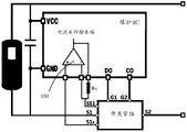
- Fig. 2 is a circuit diagram of a power source protection device in the first embodiment of the present invention.
- Fig. 3 is another circuit diagram of the power source protection device in the first embodiment of the present invention.
- FIG. 4 is a schematic structural view of a switch tube group in an embodiment of the present invention.
- FIG. 5 is a schematic structural view of another switch tube group in the embodiment of the present invention.
- FIG. 6 is a schematic structural diagram of still another switch tube group in the embodiment of the present invention.
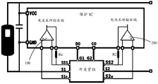
- Fig. 7 is a circuit diagram of a power source protection device in a second embodiment of the present invention.
- Fig. 8 is another circuit diagram of the power source protection device in the second embodiment of the present invention.
- the power protection device in the embodiment of the present invention is mainly applicable to various electronic products with rechargeable batteries, and is particularly suitable for some portable devices, such as mobile phones, tablet computers, notebook computers, and various wearable devices.
- a power protection device is needed to prevent power failure protection due to overvoltage, overcurrent, overcharge, etc., otherwise the battery cells in the battery may be damaged, or even cause serious explosions such as battery explosion.
- the battery involved in the embodiments of the present invention includes a rechargeable battery protection circuit or device and a battery core, and the battery core refers to an electrical energy storage carrier such as a dry battery.
- terminals For convenience of description, all electronic products having rechargeable batteries are hereinafter referred to as terminals.
- the power protection device in the embodiment of the present invention can be used as a lithium battery protection circuit for a consumer electronic device, such as a lithium battery protection circuit of various wearable devices such as a mobile phone and a watch, a notebook computer, a tablet computer, etc., and the lithium battery protection circuit exists in a piece.
- a separate printed circuit board PCB
- the PCB is connected to the cells of a lithium battery.
- Rechargeable batteries in consumer electronics generally refer to a PCB carrying a lithium battery protection circuit, a battery of a lithium battery, and a casing to form a lithium battery package for powering the consumer electronic device.
- the power protection device in the embodiment of the invention mainly comprises a MOS tube group and a protection integrated circuit (IC), which are combined to realize charging overvoltage protection, discharge undervoltage protection, charging overcurrent protection, discharge overcurrent protection,
- the utility model has the advantages that high-precision charging over-current protection and discharge over-current protection can be realized without setting a current sampling resistor on the charging/discharging circuit of the terminal, thereby greatly reducing the impedance of the through-current loop and reducing heat generation.
- the power protection device mainly uses the current mirror function of the detection field effect transistor to mirror the current in the main current loop to a small current according to a certain proportional coefficient 1/K, and the protection IC of the lithium battery completes the mirror image.
- a small current is detected and multiplied by a scaling factor K to obtain the current in the main current loop.
- K is the scaling factor
- the protection IC turns off the charging switch or the discharging switch to complete the functions of charging overcurrent protection and discharge overcurrent protection.
- the current mirroring principle of the detecting field effect transistor used in the embodiment of the present invention is to allocate the internal small switching tube unit of the switching tube group to a certain proportion on the same wafer, for example, to distribute the switching tube according to a ratio of 1 ⁇ /1000 ⁇ .
- Unit, 1000X in the 1:1000 ratio is used for main loop flow
- 1X in 1:1000 is used for current sampling, when the output pin of the two-part switch unit for main loop current and current sampling
- the overall impedance ratio of the two parts of the switch unit for the main circuit through current and current sampling should also be 1:1000, and because it is used for the main circuit through current.
- the voltages across the two parts of the current sampling unit are also equal, so the ratio of the current flowing through the main circuit and the current sampling is 1000:1.
- the terminal using the power protection device in the embodiment of the present invention includes a connector for connecting a charger through a cable, a charging management chip, a power protection device, a battery cell, and a load, wherein the power protection device
- the load may be any electrical component within the terminal, such as a display, a communication module, a processor, a memory, a sensor, and a speaker.
- the component that limits the charging current during the charging process of the terminal has a charger, a charging management chip, a protection board, and when the charger or the charging management chip fails, or both fail, the overcurrent protection of the charging of the battery is obtained. It is completed by the protection board, and when the charging overcurrent is detected, the switching element on the protection board is disconnected, and the charging path is cut off.
- the component that limits the discharge current during the discharge process is a protection plate.
- the load is abnormal, such as a load short circuit
- the overcurrent protection of the discharge of the lithium battery is completed by the protection board, and when the discharge overcurrent is detected, the switching element on the protection board is disconnected. Cut off the discharge path.
- a terminal having a charging protection function includes a battery cell, a power protection device, and a load that is powered by the battery cell.
- the power protection device mainly comprises a protection IC connected to the battery core and a switch tube group for conducting and turning off the battery core.
- the protection IC includes a power terminal VCC connected to the anode of the battery, a ground GND connected to the anode of the battery, a current detecting terminal, a current detecting terminal negative, a current sampling detecting output terminal, a discharge protection terminal DO, and a charging protection terminal CO.
- the power terminal VCC and the ground terminal GND are two power input ends of the protection IC.
- the IC protection circuit includes an operational amplifier 100, the operational amplifier 100 includes an input positive pin connected to the current detecting terminal, an input negative pin negatively connected to the current detecting terminal, and the current sampling detection The output pin to which the output is connected.
- a filter capacitor may be connected to both ends of the cell for filtering interference current and interference voltage.
- the switch in series between the negative electrode and the load cell, comprising a first connector connected to the negative terminal of the cell S 1 and a second connection to the load connection terminal S 2.
- the switch tube group further includes a discharge control terminal G1 for controlling the turn-off of the switch group during discharge and a charge control terminal G2 for controlling the switch group to be turned off during charging.
- the discharge control terminal G1 and the charge control terminal G2 are respectively connected to the discharge protection terminal DO and the charge protection terminal CO of the protection IC.
- the switch tube group further includes a sampling loop composed of a parallel sampling unit of the X sampling portions and a main circuit composed of a parallel switching unit of the KX main loop portions, wherein the X is an integer greater than or equal to 1, and K is greater than 1 value.
- X is suitable to take appropriate values, such as X is an integer value greater than or equal to 1, for example, within the value of [1, 10000], X can take values of 100, 1000, 3000 Values such as 5000 and K are greater than or equal to 100.
- K can take values greater than 1 such as 100, 500, 1000, 5000, 10000, etc.
- the comparison test can be performed according to the process, the cost, and the crystal characteristics to obtain a flow resistance of the power protection device that is small enough to obtain sufficient overcurrent protection accuracy.
- the first connecting end S 1 and the second connecting end S 2 are respectively connected to an output end and an input end respectively connected to the input end and the output end of the main circuit part of the switch tube group when charging, or
- the main circuit portion of the switch tube group constitutes a part of the charge and discharge circuit of the battery, and the current in the charge and discharge circuit mainly flows through the main circuit through the first connection end S1 and the second connection end S 2 .
- the switch tube group further includes a sampling loop detecting end connected to a connection end of the sampling loop and a main loop detecting end connected to an input or an output end of the main loop, wherein the main loop detecting end and the input The positive pin is connected, and the sampling loop detecting end is connected to the input negative pin.
- the sampling loop detecting end includes the sampling loop output terminal SS 1
- the main loop detecting end includes a detecting output terminal S 1k connected to the main loop.
- the output of the sampling circuit SS 1 through the protective current detection terminal of the operational amplifier and the negative input of IC 100 is connected to the negative pin.
- the main loop detection output S 1k is connected to the input positive pin of the operational amplifier 100 through the current detection terminal of the protection IC.
- the sampling loop output terminal SS 1 is also connected to the output pin of the operational amplifier 100, and the output pin is connected to the current sampling detection output terminal of the protection IC.
- the power protection apparatus further comprises a detecting resistor Rs sampling, the sampling detection resistor Rs connected in series between the output terminal of the sampling circuit SS 1 and an output pin of the operational amplifier 100, a current detector for generating a sample.
- the battery cell, the switch tube group and the load form a charge and discharge circuit, which is a main conduction circuit for discharging or charging the battery core.
- the sampling loop detection end further includes a sampling detection output terminal SS 1k connected to the sampling loop, and the sampling loop output terminal SS 1 is only related to the An output pin of the operational amplifier 100 is connected, and the sampling detection output terminal SS 1k is connected to an input negative pin of the operational amplifier 100, and the sampling detection resistor Rs is connected in series at the sampling circuit output terminal SS 1 and Between the output pins of the operational amplifier 100.
- the switch tube group includes (X+KX) switch tube units connected in parallel with each other, wherein X MOS switch tube units are connected in parallel to form the sampling loop, and KX MOS tubes are connected in parallel to form the main loop.
- Each of the switch tube units includes a first switch tube Sa and a second switch tube Sb connected in series with the Sa, wherein each of the Sa or Sb is connected in parallel with a diode D1, wherein the Sa and the Sb Any one of the charging switch tube and the other is a discharge switch tube.
- the Sa is selected as a discharge switch tube, which is turned on when the battery core is discharged and the battery core is discharged.
- the Sb When it is turned off, the Sb is a charging switch tube that is turned on when the battery is charged and turned off when the battery is discharged.
- the D1 is used to protect the Sa and Sb from being broken down.
- the Sa and Sb may be MOS tubes or other semiconductor switching tubes having similar characteristics.
- the X switch tube units are connected in parallel to form the sampling loop, and the KX switch tube units are connected in parallel to form the main loop, wherein the (X+KX) switch tube units of Sa and Sb
- the D poles are connected together, and the G poles of Sa of the (X+KX) switch tube units are connected together to form the discharge control terminal G1, and the G pole connection of the Sb of the (X+KX) switch tube unit
- the charging control terminal G2 is formed together.
- the S poles of all Sa in the X switch tube units constituting the sampling loop are connected to the same pin, and the lead circuit is taken out to form the sampling loop output terminal SS 1 , and all of the X switch tube units
- the S pole of Sb is connected to the same pin, and is led out by the pin to form the sampling loop output terminal SS 2 .
- the sampling detection output terminal SS 1k of the switching tube group can be directly connected to all the Sa wafers in the X switching tube units of the sampling loop by the high conductivity metal wire. Formed on the upper S pole.
- another sampling detection output SS 2k of the switching tube group can be formed by directly connecting a high conductivity metal to the S pole on the wafer of all Sbs of the X switching tube units of the sampling loop.
- the detection output S 1k of the main loop can be formed by directly connecting the high conductivity metal wires to the S poles on all of the Sa's wafers in the KX switching tube units of the main circuit.
- the other detection output S 2k of the main circuit of the switching tube group can be formed by directly connecting the high conductivity metal to the S pole on the wafer of all Sbs in the KX switching tube units of the main circuit.
- the high conductivity metal wires include high conductivity metal wires such as gold, silver, and copper, and may also include some high conductivity alloy conductors.
- the primary loop detection end may be a first connection end S1 of all Sas connected to a main loop in the switch tube group, and a first connection end of all Sbs connecting the main loops in the switch tube group. Two connection ends Sb.
- the positions of the Sa and Sb may be interchanged, and the operational amplifier 100 may also be connected to the other side of the switch tube group, that is, the switch tube may be associated with SS 2 , SS 2k , and S 2k connection.
- the difference in the connection method does not bring about the implementation principle and the change of the mode, and will not be described here.
- the switch tube group is not limited to each of the switch unit tube units shown in FIG. 4, and includes the Sa and Sb.
- the switch tube group is a unidirectional switch.
- the tube group, each switch tube unit includes only one switch tube, and only protects the charging or discharging of the battery cells.
- the switch tube group is a bidirectional switch tube group, but only each switch tube unit of the main loop portion of the switch tube group includes two reverse units.
- the switching tubes are connected in series, and each switching unit of the sampling loop portion of the switching tube group includes only one switching tube.
- the switch tube group in the embodiment of the present invention is not limited to a specific structural design, and can be used as the switch of the embodiment of the present invention as long as the mirror relationship of the current ratio in the equal pressure between the main circuit and the sampling circuit can be realized. Tube group.
- the operational amplifier 100 is configured to adjust the potential of the input negative pin and the input positive pin to be the same, that is, to make the sampling detection output end SS 1k of the switch tube group and the detection output end S of the main circuit
- the I S1k is substantially equal to the current I S1 flowing through the switching tube group and the entire charging and discharging circuit
- the protection IC determines whether to issue a shutdown signal to the switch tube group discharge control terminal G1 and the charge control terminal G2 according to the size of I S1k to turn off the switch tube group to stop charging or discharging of the battery cell.
- the embodiment of the invention combines the switch tube group and the protection IC to realize charging overvoltage protection, discharge undervoltage protection, charging overcurrent protection, discharge overcurrent protection of the battery, and utilizing a current mirror function of detecting a field effect transistor,
- the current in the main current loop is mirrored to a small current according to a certain proportional coefficient 1/K.
- the lithium battery protection IC completes the detection of the small current generated by the image, and multiplies the proportional coefficient K to obtain The amount of current in the main flow loop.
- the sampling detection resistor Rs is connected in series between the sampling detection output terminal SS 1k and the output pin, not on the charging and discharging circuit, and the detection current flowing through the sampling detecting resistor Rs is the charging and discharging.
- the current of the current on the loop is much smaller than the current on the charge and discharge circuit. Therefore, the heat generated by the sampling and detecting resistor Rs is also very small, and the temperature of the charge and discharge circuit is substantially not practical. Sexual influence.
- the sampling detection output terminal SS 1k and the sampling detection resistor Rs is much smaller than the current flowing through the main circuit of the switching tube group and the charging and discharging circuit, although the sampling detection The value of the resistor Rs is tens of ohms to several hundred ohms, and the loss of the practical influence is not generated on the sampling detecting resistor Rs, and the resistance of the sampling detecting resistor Rs is not affected by heat or the like. The effect is advantageous to select the appropriate resistance to achieve maximum detection accuracy.
- the protection IC determines whether to charge an overcurrent or a discharge overcurrent according to the detection current, and further, the protection IC turns off the charging switch or the discharging switch, thereby completing the functions of charging overcurrent protection and discharging overcurrent protection, thereby eliminating the need for
- the current sampling resistor on the charging and discharging circuit of the terminal can realize high-precision charging over-current protection and discharge over-current protection, and can greatly reduce the impedance of the current-passing loop and effectively reduce the heat generation of the charging and discharging circuit.
- the power protection device is configured to determine that the accuracy of the comparator reference voltage of the overcurrent can reach a level of XmV ⁇ 2 mV. For example, 200mV ⁇ 2mV, then the error caused by the accuracy of the comparator reference voltage used by the power protection device to determine the overcurrent is only 1%. For example, according to the threshold of 7 ⁇ 0.7A (A) and overcurrent protection for 3.5 seconds (S), it can meet the protection of 8A in 5S, while 5A is within 60S and 6A is within 5S. 7A does not require shutdown protection within 2S.
- 0.7A is 10% accuracy for 7A, and the error caused by the accuracy of the protection IC can be less than 1% in the 10% error, and the error caused by the precision accuracy of the current sampling resistor can be achieved. Within 1%, the error caused by the proportional accuracy of the current mirror of the MOS tube group can be within 5%, so that the cumulative target reaches less than 10%.
- the output of the comparator When the second terminal voltage of the sampling detecting resistor Rs, that is, the amplitude of the measured signal is greater than the comparator reference voltage used by the protection IC to determine an overcurrent, the output of the comparator outputs a first level, and further Turning off the switch tube group, indicating that the charge and discharge circuit and the current in the switch tube group are overcurrent, otherwise, outputting the second level to maintain the switch tube group on, indicating the charge and discharge circuit and the The current in the switching tube group is not overcurrent.
- the power protection device can be used for current or voltage abnormal protection of a power source or device other than the battery core, and the abnormality of the detection current of the power source or the device is too large or too small to start and turn off. Protection measures such as decompression or boosting.
- the power protection device according to the second embodiment of the present invention is different from the power protection device of the first embodiment in that the power protection device of the first embodiment has only one operational amplifier 100, and the operational amplifier 100 is only connected to the output end of the discharge switch tube Sa in the switch tube group, and the second embodiment further includes a slave operational amplifier 200 connected to the switch tube group according to the first embodiment.
- the output of the charging switch Sb is as follows:
- the protection IC further includes a current detecting terminal, a current detecting terminal negative, and a current sampling detecting output terminal according to the first embodiment.
- the slave operational amplifier 200 also includes an input positive pin that is coupled to the current sense terminal, an input negative pin that is negatively coupled to the current sense terminal, and an output pin that is coupled to the current sense detection output.
- the sampling loop output terminal SS 2 of the switching tube group is connected to the input negative pin of the slave operational amplifier 200 through a current detecting terminal of the protection IC, and the detection output terminal S 2k of the main circuit passes the protection
- the current sense terminal of the IC is being coupled to the input positive pin of the slave operational amplifier 200.
- the sampling loop output terminal SS 2 is connected to the output pin of the slave operational amplifier 200, and the output pin is connected to the current sampling detection output terminal of the protection IC.
- the power protection device further includes a sampling detection resistor Rs connected in series between the sampling loop output terminal SS 2 of the switching tube group and the output pin of the slave operational amplifier 200 for generating Sampling and detecting current.
- the slave operational amplifier 200 of the second embodiment of the present invention is similar in connection to the operational amplifier 100 of the first embodiment, wherein the fine distinction has been as described above.
- the current detection and overcurrent protection principles of the charging and discharging circuit in the second embodiment of the present invention are completely the same as those in the first embodiment, and are not described herein again.
- the sampling loop output terminal SS2 is only connected to the output pin of the slave operational amplifier 200, and the sampling detection output terminal SS 2k Connected to the input negative pin of the slave operational amplifier 200, and the sampling sense resistor Rs is connected in series between the sampling loop output terminal SS2 and the output pin of the slave operational amplifier 200.
- the protection IC has only one slave operational amplifier 200 connected to the output terminal of the charging switch tube Sb of the switch tube group, and the invention can also be implemented to achieve the use of the mirror current.
- the detection current is used to detect the charging and discharging current value of the battery cell, and the switching of the switching tube group is controlled according to the charging and discharging current value obtained by the sampling detection and the comparison result of the comparator to realize abnormal protection of the overcurrent, overheating and the like.
Landscapes
- Engineering & Computer Science (AREA)
- Power Engineering (AREA)
- Physics & Mathematics (AREA)
- General Physics & Mathematics (AREA)
- Protection Of Static Devices (AREA)
- Secondary Cells (AREA)
- Charge And Discharge Circuits For Batteries Or The Like (AREA)
Abstract
L'invention concerne un appareil de protection d'alimentation électrique d'un appareil de protection de batterie, lequel appareil de protection de batterie est utilisé pour protéger une cellule de batterie connectée à une charge. L'appareil de protection d'alimentation électrique comprend un circuit intégré de protection, un groupe de tubes de commutation et une résistance d'échantillonnage, le CI de protection comprenant deux extrémités d'entrée d'alimentation électrique, qui sont respectivement connectées à des pôles positif et négatif de la cellule de batterie, et un amplificateur opérationnel ; l'amplificateur opérationnel comprend une broche positive d'entrée, une broche négative d'entrée et une broche de sortie ; le groupe de tubes de commutation est connecté entre le pôle négatif de la cellule de batterie et la charge, et est utilisé pour commander la connexion et la déconnexion d'une boucle de charge et de décharge de la cellule de batterie ; le groupe de tubes de commutation comprend une boucle principale et une boucle d'échantillonnage, et le groupe de tubes de commutation comprend une première extrémité de connexion, qui est connectée au pôle négatif de la cellule de batterie, une seconde extrémité de connexion, qui est connectée à la charge, une extrémité de commande, une extrémité de détection de boucle d'échantillonnage et une extrémité de détection de boucle principale, l'extrémité de commande étant connectée au CI de protection ; la résistance de détection d'échantillonnage Rs étant connectée en série entre l'extrémité de détection de boucle d'échantillonnage et la broche de sortie ; et l'extrémité de détection de boucle principale est connectée à la broche positive d'entrée, et l'extrémité de détection de boucle d'échantillonnage est connectée à la broche négative d'entrée.
Priority Applications (3)
| Application Number | Priority Date | Filing Date | Title |
|---|---|---|---|
| EP18858998.0A EP3675303A4 (fr) | 2017-09-23 | 2018-09-21 | Appareil de protection d'alimentation électrique et terminal faisant appel à celui-ci |
| US16/825,061 US11527883B2 (en) | 2017-09-23 | 2020-03-20 | Power protection apparatus and terminal using the apparatus |
| US17/992,216 US12470057B2 (en) | 2017-09-23 | 2022-11-22 | Power protection apparatus and terminal using the apparatus |
Applications Claiming Priority (2)
| Application Number | Priority Date | Filing Date | Title |
|---|---|---|---|
| CN201710870503.8 | 2017-09-23 | ||
| CN201710870503.8A CN108063428B (zh) | 2017-09-23 | 2017-09-23 | 一种电源保护装置以及使用所述装置的终端 |
Related Child Applications (1)
| Application Number | Title | Priority Date | Filing Date |
|---|---|---|---|
| US16/825,061 Continuation US11527883B2 (en) | 2017-09-23 | 2020-03-20 | Power protection apparatus and terminal using the apparatus |
Publications (1)
| Publication Number | Publication Date |
|---|---|
| WO2019057144A1 true WO2019057144A1 (fr) | 2019-03-28 |
Family
ID=62137334
Family Applications (1)
| Application Number | Title | Priority Date | Filing Date |
|---|---|---|---|
| PCT/CN2018/106907 Ceased WO2019057144A1 (fr) | 2017-09-23 | 2018-09-21 | Appareil de protection d'alimentation électrique et terminal faisant appel à celui-ci |
Country Status (4)
| Country | Link |
|---|---|
| US (2) | US11527883B2 (fr) |
| EP (1) | EP3675303A4 (fr) |
| CN (2) | CN110416976A (fr) |
| WO (1) | WO2019057144A1 (fr) |
Families Citing this family (7)
| Publication number | Priority date | Publication date | Assignee | Title |
|---|---|---|---|---|
| CN110416976A (zh) | 2017-09-23 | 2019-11-05 | 华为技术有限公司 | 一种电源保护装置以及使用所述装置的终端 |
| CN112986635B (zh) * | 2019-12-18 | 2023-04-07 | 上海比亚迪有限公司 | 可编程电子负载和电池测试装置 |
| CN113300426A (zh) * | 2021-04-27 | 2021-08-24 | 珠海迈巨微电子有限责任公司 | 功率器件、电池管理系统及检测电路 |
| CN113922338A (zh) * | 2021-10-15 | 2022-01-11 | 东莞市安泰电子科技有限公司 | 一种电池过电流保护电路 |
| CN117991071A (zh) * | 2022-05-24 | 2024-05-07 | 上海沛塬电子有限公司 | 一种高精度电流检测的开关集成芯片及芯片模组 |
| CN118868339B (zh) * | 2024-09-26 | 2025-04-11 | 浙江欣旺达电子有限公司 | 电池保护方法、装置及充放电回路 |
| CN120281063B (zh) * | 2025-04-01 | 2025-10-03 | 北京金河水务建设集团有限公司 | 用于水利供电的双电源自动投切设备及控制系统 |
Citations (8)
| Publication number | Priority date | Publication date | Assignee | Title |
|---|---|---|---|---|
| JP2004282894A (ja) * | 2003-03-14 | 2004-10-07 | Fujitsu Access Ltd | 充放電装置 |
| CN102208802A (zh) * | 2010-06-29 | 2011-10-05 | 上海山景集成电路技术有限公司 | 功率开关管过流检测和过流保护电路 |
| CN103529276A (zh) * | 2013-10-28 | 2014-01-22 | 无锡中星微电子有限公司 | 电流检测电路及充电电池 |
| CN103575964A (zh) * | 2012-07-19 | 2014-02-12 | 快捷半导体(苏州)有限公司 | 一种功率开关管的过流检测电路和方法 |
| CN103633617A (zh) * | 2013-12-02 | 2014-03-12 | 嘉兴中润微电子有限公司 | 一种应用于大功率电机驱动芯片的过流保护检测电路 |
| CN105846493A (zh) * | 2016-04-19 | 2016-08-10 | 无锡中感微电子股份有限公司 | 过流检测、保护电路及电池 |
| CN107579508A (zh) * | 2017-09-23 | 2018-01-12 | 华为技术有限公司 | 一种电源保护装置以及使用所述装置的终端 |
| CN108063428A (zh) * | 2017-09-23 | 2018-05-22 | 华为技术有限公司 | 一种电源保护装置以及使用所述装置的终端 |
Family Cites Families (23)
| Publication number | Priority date | Publication date | Assignee | Title |
|---|---|---|---|---|
| JP4288590B2 (ja) * | 2003-12-02 | 2009-07-01 | 富士電機デバイステクノロジー株式会社 | 双方向スイッチの電流検出回路 |
| CA2531295C (fr) * | 2004-12-22 | 2013-10-22 | Odyne Corporation | Systeme de charge de batterie faisant appel a une porteuse sur cable d'alimentation et a un systeme de gestion d'accumulateurs |
| US7960997B2 (en) * | 2007-08-08 | 2011-06-14 | Advanced Analogic Technologies, Inc. | Cascode current sensor for discrete power semiconductor devices |
| JP5592073B2 (ja) * | 2009-02-09 | 2014-09-17 | 富士電機株式会社 | 双方向スイッチの電流検出回路 |
| JP5477304B2 (ja) * | 2011-01-25 | 2014-04-23 | トヨタ自動車株式会社 | 電源システムおよびそれを搭載する車両、ならびに電源システムの制御方法 |
| CN102355018A (zh) | 2011-09-14 | 2012-02-15 | 开源集成电路(苏州)有限公司 | 一种锂电池充电保护芯片 |
| CN103187712B (zh) | 2011-12-27 | 2017-02-22 | 海洋王照明科技股份有限公司 | 电池充放电保护电路 |
| JP5870763B2 (ja) | 2012-03-02 | 2016-03-01 | ミツミ電機株式会社 | 二次電池監視装置および電池パック |
| CN204030643U (zh) * | 2013-06-01 | 2014-12-17 | 快捷半导体(苏州)有限公司 | 用于电池管理和保护的系统及设备 |
| CN203713590U (zh) * | 2014-01-26 | 2014-07-16 | 方贵龙 | 一种并联式大功率电动汽车直流充电电源系统 |
| CN103954825B (zh) | 2014-03-28 | 2016-08-31 | 无锡中感微电子股份有限公司 | 一种过流检测电路 |
| CN204068213U (zh) * | 2014-05-30 | 2014-12-31 | 无锡中星微电子有限公司 | 一种锂电池保护系统及其过流检测电路 |
| CN104022490B (zh) | 2014-05-30 | 2017-03-15 | 无锡中感微电子股份有限公司 | 一种锂电池保护系统及其过流检测电路 |
| TWI661631B (zh) * | 2014-11-20 | 2019-06-01 | Upi Semiconductor Corp. | 電池保護裝置與其操作方法 |
| CN204465038U (zh) * | 2015-01-16 | 2015-07-08 | 荆延杰 | 一种串联电池组充放电均衡电路 |
| CN104682429B (zh) | 2015-02-04 | 2017-04-19 | 国家电网公司 | 一种电压源逆变器并联控制系统 |
| CN204666703U (zh) | 2015-04-14 | 2015-09-23 | 东莞市德尔能新能源股份有限公司 | 快充电池保护板的电流检测电路 |
| JP5850197B1 (ja) * | 2015-06-17 | 2016-02-03 | ミツミ電機株式会社 | 電池保護集積回路及び回路特性設定方法 |
| CN204794046U (zh) * | 2015-08-01 | 2015-11-18 | 深圳市三和朝阳科技有限公司 | 聚合物电池保护板电路 |
| CN205029381U (zh) * | 2015-09-28 | 2016-02-10 | 新源国宏科技(北京)有限公司 | 一种具有二次保护功能的数字bms保护板 |
| CN205231808U (zh) | 2015-12-24 | 2016-05-11 | 惠州市盛微电子有限公司 | 手机锂电池保护电路 |
| CN105680422B (zh) * | 2016-04-07 | 2018-06-15 | 无锡中感微电子股份有限公司 | 改进型电池保护电路及系统 |
| CN206516635U (zh) | 2016-12-15 | 2017-09-22 | 深圳市锐骏半导体股份有限公司 | 带电流检测功能的场效应管 |
-
2017
- 2017-09-23 CN CN201910589913.4A patent/CN110416976A/zh active Pending
- 2017-09-23 CN CN201710870503.8A patent/CN108063428B/zh active Active
-
2018
- 2018-09-21 EP EP18858998.0A patent/EP3675303A4/fr active Pending
- 2018-09-21 WO PCT/CN2018/106907 patent/WO2019057144A1/fr not_active Ceased
-
2020
- 2020-03-20 US US16/825,061 patent/US11527883B2/en active Active
-
2022
- 2022-11-22 US US17/992,216 patent/US12470057B2/en active Active
Patent Citations (8)
| Publication number | Priority date | Publication date | Assignee | Title |
|---|---|---|---|---|
| JP2004282894A (ja) * | 2003-03-14 | 2004-10-07 | Fujitsu Access Ltd | 充放電装置 |
| CN102208802A (zh) * | 2010-06-29 | 2011-10-05 | 上海山景集成电路技术有限公司 | 功率开关管过流检测和过流保护电路 |
| CN103575964A (zh) * | 2012-07-19 | 2014-02-12 | 快捷半导体(苏州)有限公司 | 一种功率开关管的过流检测电路和方法 |
| CN103529276A (zh) * | 2013-10-28 | 2014-01-22 | 无锡中星微电子有限公司 | 电流检测电路及充电电池 |
| CN103633617A (zh) * | 2013-12-02 | 2014-03-12 | 嘉兴中润微电子有限公司 | 一种应用于大功率电机驱动芯片的过流保护检测电路 |
| CN105846493A (zh) * | 2016-04-19 | 2016-08-10 | 无锡中感微电子股份有限公司 | 过流检测、保护电路及电池 |
| CN107579508A (zh) * | 2017-09-23 | 2018-01-12 | 华为技术有限公司 | 一种电源保护装置以及使用所述装置的终端 |
| CN108063428A (zh) * | 2017-09-23 | 2018-05-22 | 华为技术有限公司 | 一种电源保护装置以及使用所述装置的终端 |
Non-Patent Citations (1)
| Title |
|---|
| See also references of EP3675303A4 * |
Also Published As
| Publication number | Publication date |
|---|---|
| CN108063428B (zh) | 2019-07-12 |
| US20200220346A1 (en) | 2020-07-09 |
| US11527883B2 (en) | 2022-12-13 |
| EP3675303A4 (fr) | 2020-09-02 |
| EP3675303A1 (fr) | 2020-07-01 |
| US20230090857A1 (en) | 2023-03-23 |
| US12470057B2 (en) | 2025-11-11 |
| CN108063428A (zh) | 2018-05-22 |
| CN110416976A (zh) | 2019-11-05 |
Similar Documents
| Publication | Publication Date | Title |
|---|---|---|
| WO2019057148A1 (fr) | Appareil de protection de source d'alimentation électrique et terminal l'utilisant | |
| CN108063428B (zh) | 一种电源保护装置以及使用所述装置的终端 | |
| TWI680621B (zh) | 電池保護電路及包含其之電池組 | |
| KR100337905B1 (ko) | 전기적 파라미터를 감지하는 합체형 저항기 | |
| CN105846493B (zh) | 过流检测、保护电路及电池 | |
| JP2018533019A (ja) | 抗短絡検出装置およびユーザ端末 | |
| WO2017201740A1 (fr) | Carte de protection de pile, pile et terminal mobile | |
| US10355497B2 (en) | Protection of parallel connected cells in battery packs | |
| KR20190032882A (ko) | 배터리 보호 회로 | |
| CN104184177A (zh) | 电子装置及其充电控制电路 | |
| CN114696378A (zh) | 一种电池快充装置、锂离子电池和电子设备 | |
| KR102320110B1 (ko) | 하나의 전류 센싱 저항을 갖는 배터리 보호 회로 | |
| CN215870843U (zh) | 电流检测装置、半导体芯片、电池管理系统及用电设备 | |
| WO2016110130A1 (fr) | Accumulateur et son système d'alimentation électrique | |
| JP6834527B2 (ja) | 充放電装置 | |
| CN113125830B (zh) | 一种双向电流检测电路和电源系统 | |
| WO2021093357A1 (fr) | Circuit de protection contre les surintensités de charge/décharge et procédé de protection contre les surintensités correspondant | |
| CN218216722U (zh) | 一种温度保护电路及系统 | |
| CN113141050A (zh) | 电子设备 | |
| CN209894891U (zh) | 用于电子设备的接电检测装置 | |
| CN105842521A (zh) | 充电式便携低采样压降的μA微电流监测系统 | |
| CN120784488A (zh) | 电池、电池的控制方法、控制电路以及电子设备 | |
| CN115480198A (zh) | 一种bms锂电池管理系统测试装置及测试平台 | |
| CN113675922A (zh) | 电流检测装置、半导体芯片、电池管理系统及用电设备 | |
| CN118693769A (zh) | 电源防护电路、电源装置及水下机器人设备 |
Legal Events
| Date | Code | Title | Description |
|---|---|---|---|
| 121 | Ep: the epo has been informed by wipo that ep was designated in this application |
Ref document number: 18858998 Country of ref document: EP Kind code of ref document: A1 |
|
| NENP | Non-entry into the national phase |
Ref country code: DE |
|
| ENP | Entry into the national phase |
Ref document number: 2018858998 Country of ref document: EP Effective date: 20200325 |