WO2019058932A1 - Dispositif d'antenne - Google Patents
Dispositif d'antenne Download PDFInfo
- Publication number
- WO2019058932A1 WO2019058932A1 PCT/JP2018/032371 JP2018032371W WO2019058932A1 WO 2019058932 A1 WO2019058932 A1 WO 2019058932A1 JP 2018032371 W JP2018032371 W JP 2018032371W WO 2019058932 A1 WO2019058932 A1 WO 2019058932A1
- Authority
- WO
- WIPO (PCT)
- Prior art keywords
- opening
- dielectric layer
- slot
- antenna device
- viewed
- Prior art date
- Legal status (The legal status is an assumption and is not a legal conclusion. Google has not performed a legal analysis and makes no representation as to the accuracy of the status listed.)
- Ceased
Links
Images






Classifications
-
- H—ELECTRICITY
- H01—ELECTRIC ELEMENTS
- H01Q—ANTENNAS, i.e. RADIO AERIALS
- H01Q13/00—Waveguide horns or mouths; Slot antennas; Leaky-waveguide antennas; Equivalent structures causing radiation along the transmission path of a guided wave
- H01Q13/08—Radiating ends of two-conductor microwave transmission lines, e.g. of coaxial lines, of microstrip lines
-
- H—ELECTRICITY
- H01—ELECTRIC ELEMENTS
- H01Q—ANTENNAS, i.e. RADIO AERIALS
- H01Q21/00—Antenna arrays or systems
- H01Q21/06—Arrays of individually energised antenna units similarly polarised and spaced apart
Definitions
- the present invention relates to an antenna device.
- Priority is claimed on Japanese Patent Application No. 2017-181338, filed September 21, 2017, the content of which is incorporated herein by reference.
- an antenna apparatus provided with a planar antenna of an electromagnetic coupling feed system is known.
- the present invention has been made in view of the above problems, and provides an antenna device capable of reducing reflection loss even when using a planar antenna of an electromagnetic coupling feed system.
- an antenna device comprising: a first dielectric layer; and a flat plate disposed on a first surface of the first dielectric layer and including an electrode portion for electromagnetic coupling.
- a patch antenna, and a nonconductor portion disposed on a second surface opposite to the first surface in the first dielectric layer, and extending in a first direction at a position facing the electrode portion
- a ground conductor plate in which a slot is formed a second dielectric layer fixed to the ground conductor plate so as to face the first dielectric layer with the ground conductor plate interposed therebetween, and the second dielectric layer A second direction formed on the second dielectric layer so as to face the ground conductor plate with a body layer interposed therebetween, and having a tip intersecting with the first direction when viewed in the normal direction of the patch antenna
- a linear feed conductor disposed in a positional relationship that intersects the slot when viewed in the normal direction.
- the slot is connected in communication with a first opening having a constant first width in the
- the second opening may be polygonal as viewed from the normal direction.
- the second opening may be circular as viewed from the normal direction.
- the power feeding conductor is the first portion of the first opening when viewed from the normal direction.
- the tip of the feeding conductor is equal to the length of the first opening in the first direction from the center of the first opening in the second direction. It may be formed at a position.
- the second direction is orthogonal to the first direction
- the power feeding conductor The tip may be arranged to be orthogonal to the slot when viewed in the normal direction.
- FIG. 1 is a schematic exploded perspective view showing an example of the antenna device of the present embodiment.
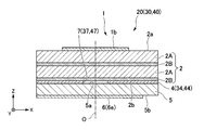
- FIG. 2 is a schematic longitudinal sectional view showing an example of the configuration of the main part of the antenna device of the present embodiment.
- FIG. 3 is a schematic plan view showing an example of a patch antenna of the antenna device of the present embodiment.
- FIG. 4 is a schematic plan view showing the positional relationship between the feed conductor and the slot in the antenna device of the present embodiment.
- FIG. 5 is a schematic plan view showing an example of the opening shape of the slot used in the antenna device of the present embodiment.
- Each drawing is a schematic view, and dimensions and shapes are exaggerated or simplified (the same applies to the other drawings below).
- the antenna device 20 of the present embodiment shown in FIG. 1 includes a planar antenna of an electromagnetic coupling feed system.
- the antenna device 20 can be used as an antenna device in communication in the IoT (Internet of Things) field or in high-speed wireless communication such as WiGig (Wireless Gigabit).
- IoT Internet of Things
- WiGig Wireless Gigabit
- the patch antenna 1, the first dielectric layer 2, the ground conductor plate 4, the second dielectric layer 5, and the feeding conductor 6 are stacked in this order. ing.
- the stacking direction is referred to as the Z-axis direction
- biaxial directions orthogonal to the Z-axis direction and orthogonal to each other will be referred to as an X-axis direction (second direction) and a Y-axis direction (first direction).
- the coordinate system here is right-handed.
- each patch antenna 1 is patterned on a first surface 2a (first surface) of a first dielectric layer 2 described later based on a predetermined arrangement pattern.
- the normal direction of the patch antenna 1 and the first surface 2a is the Z-axis direction.
- the patch antenna 1 is a flat antenna electromagnetically coupled and fed from a feed conductor 6 described later.
- the shape of each patch antenna 1 is not particularly limited.
- a plurality of patch antennas 1 are, for example, arranged in the form of a square grid arranged in the X-axis direction and the Y-axis direction. Specifically, 64 patch antennas 1 are arranged in a square grid of 8 ⁇ 8.
- each patch antenna 1 includes, as an example, four radiating elements 1 a and a divided circuit pattern 1 d which is a divider for arraying the respective radiating elements 1 a.
- Each of the radiation elements 1a is formed in a rectangular shape having sides extending in the X-axis direction and the Y-axis direction.
- the respective radiation elements 1a are arranged in a rectangular grid shape which is a substantially square grid arranged in the X-axis direction and the Y-axis direction.
- the divided circuit pattern 1 d includes an electrode portion 1 b for electromagnetic coupling, and four wiring portions 1 c that electrically connect the electrode portion 1 b and the radiation elements 1 a to each other.
- the electrode portion 1b is formed in a rectangular shape extending in the X-axis direction centering on an intersection of diagonals connecting centers of arrangement positions of the radiation elements 1a.
- the feeding point in the electrode portion 1b is formed at the center of the electrode portion 1b.
- Each wiring portion 1c extends from the side portion in the Y-axis direction at the four corner portions of the electrode portion 1b toward the radiation element 1a connected thereto. Specifically, each wiring portion 1c extends in the Y-axis direction toward the radiation element 1a to which each wiring portion 1c is connected, and then a position facing the central portion of the side portion in the X-axis direction of the radiation element 1a to which each is connected In the direction of the X axis. Therefore, the path lengths of the wiring portions 1c are equal to one another.
- each patch antenna 1 having such a configuration is disposed at a corner of a rectangular area having a width W X in the X-axis direction and a width W Y in the Y-axis direction.
- W x and W y may be 4.4 mm and 4.52 mm, respectively.
- the width W aX in the X-axis direction of the radiating elements 1a, the width in the Y-axis direction W aY, respectively, 1.15 mm may be 1.15 mm.
- the width W bX in the X-axis direction of the electrode portion 1 b and the width W bY in the Y-axis direction may be 0.8 mm or 0.4 mm, respectively.
- the line width of each wiring portion 1c may be 0.13 mm.
- the quarter effective length (hereinafter simply referred to as the effective length) of such a patch antenna 1 is 1.15 mm.
- the patch antenna 1 is formed of, for example, a metal material such as copper.
- the first dielectric layer 2 is a flat member having a dielectric constant and a layer thickness defined in accordance with the required radiation characteristics.
- the first dielectric layer 2 may be a single layer dielectric, or a plurality of dielectrics may be bonded. Whether to use a single layer or multiple layers may be determined in consideration of, for example, the material cost.
- the example shown in FIG. 2 shows an example in which the dielectric 2A having a certain thickness is bonded by the resin adhesive layer 2B which is a dielectric.
- a second surface 2b (second surface) which is a surface opposite to the first surface 2a in the first dielectric layer 2, is formed of a resin adhesive layer 2B.
- the resin adhesive layer 2B constituting the second surface 2b joins a ground conductor plate 4 described later.
- the ground conductor plate 4 is a plate member of a conductor in which slots 7 are formed at positions facing the patch antennas 1.
- the ground conductor plate 4 is grounded.
- the ground conductor plate 4 is fixed to the first dielectric layer 2 via the resin adhesive layer 2B constituting the second surface 2b.
- the slot 7 is a nonconductor in the ground conductor plate 4. As shown in FIGS. 3 and 4, the slot 7 extends in the Y-axis direction which is the first direction.
- the opening shape of the slot 7 is a shape capable of achieving impedance matching between the impedance of the patch antenna 1 and the feeding conductor 6 described later.
- the slot 7 in this embodiment is H-shaped as viewed from the Z-axis direction, as shown in FIG. Specifically, the slot 7 has a rectangular first opening 7a and second openings 7b formed at both ends in the longitudinal direction (first direction) of the first opening 7a, Equipped with As shown in FIG.
- the center (centre) of the slot 7 is disposed so as to overlap with the center (centre) of the electrode portion 1 b of the patch antenna 1. Therefore, when viewed from the Z-axis direction, the slot 7 is orthogonal to the centers of the electrode portion 1b and the electrode portion 1b, and traverses the electrode portion 1b in the Y-axis direction.
- the first opening 7a constitutes a passing signal portion through which a signal passes.
- Each second opening 7 b is an opening that increases the impedance at both ends of the passing signal portion. More preferably, the length d3 of the slot 7 in the longitudinal direction (first direction) is adjusted to the effective length of the patch antenna 1.
- the width W2 in the short direction of the first opening 7a is more preferably 0.75 mm, for example, in order to set the coupling impedance to 112 ⁇ .
- W2 is more preferably 0.2 mm.
- Each second opening 7b is provided in a shape that widens from the width W2 in the short direction of the first opening 7a in order to form an impedance larger than the coupling impedance by the first opening 7a.
- each second opening 7b is a rectangle having a length d2 in the Y-axis direction and a width W3 in the X-axis direction (where W3> W2).
- d2 and W3 may be 0.2 mm and 0.4 mm, respectively.
- the coupling impedance of the electromagnetic coupling feeding portion is 112 ⁇ at the central portion of the electrode portion 1 b.
- the second dielectric layer 5 is fixed to the ground conductor plate 4 and the feeding conductor 6 to be described later so that the patch antenna 1 can be electromagnetically fed from the feeding conductor 6 to be described later through the slot 7. It is provided to be separated by the insulation distance of. For this reason, the ground conductor plate 4 is disposed on the first surface 5 a of the second dielectric layer 5, and the feeding conductor 6 described later is disposed on the second surface 5 b of the second dielectric layer 5. It is done.
- the relative permittivity ⁇ r of the second dielectric layer 5 is preferably as small as possible.
- the relative dielectric constant ⁇ r of the second dielectric layer 5 is more preferably 1 or more and 2.5 or less.
- the layer thickness of the second dielectric layer 5 is more preferably 130 ⁇ m.
- the feeding conductor 6 is patterned on the second surface 5 b of the second dielectric layer 5.
- the feed conductor 6 can be electrically connected to an external circuit (not shown) via a connection path having a predetermined impedance.
- a plurality of tip lines 6e formed on the tip of the feed conductor 6 so as to overlap with the slots 7 and the electrode portions 1b of the patch antennas 1 as viewed from the Z-axis direction The tip portion is formed.
- Each tip line 6 e is a linear conductor that constitutes the open end of the feed conductor 6.
- each tip end line 6 e extends in the X axis direction, passing through the longitudinal center of the first opening 7 a of each slot 7 when viewed from the Z axis direction. . Therefore, when viewed from the Z-axis direction, the tip end line 6e crosses the first opening 7a so as to be orthogonal to the first opening 7a.
- the line width W1 of the tip line 6e is such that a very wide line width leads to more losses and radiation, and a very thin line width makes it difficult to manufacture, thus minimizing production and back radiation It has been decided as such.
- the line width W1 of the tip end line 6e may be 0.1 mm.
- the length (stub length) from the central axis O of the first opening 7a to the end 6f of the end track 6e is ds.
- the stub length ds is made equal to the length d1 of the first opening 7a.
- the stub length ds is 0.75 mm.
- each of the tip lines 6e two tip lines 6e adjacent in the Y-axis direction are connected to each other by a first line 6d extending in the Y-axis direction at an end opposite to the tip 6f. ing.
- the line width of each first line 6d is equal to the line width W1 of the tip line 6e.
- the two first lines 6d adjacent to each other in the X-axis direction are connected to each other by a second line 6c extending in the X-axis direction at a position where each of the lengths in the longitudinal direction is equally divided into two.
- the line width of each second line 6c is equal to the line width W1 of the tip end line 6e except for both ends in the longitudinal direction.
- a widened portion 6b in the vicinity of a connection portion with the first line 6d, a widened portion 6b whose line width is widened stepwise from W1 is formed.
- the widening portion 6 b in the present embodiment is provided to optimize the impedance of the power supply conductor 6.
- the line width of the widened portion 6b is widened in three steps such as W11, W12, and W13 (where W11 ⁇ W12 ⁇ W13) from the middle portion to the end portion of the second line 6c.
- the length of each portion of the line widths W11, W12, and W13 is L11, L12, and L13.
- the line widths W11, W12, and W13 may be 0.12 mm, 0.22 mm, and 0.3 mm, respectively.
- the lengths L11, L12, and L13 may all be 0.5 mm.
- the third line 6a having a line width W1 is connected to a position at which the length in the longitudinal direction of the second line 6c is divided into two equally.
- the third line 6a connects a group of four tip lines 6e adjacent to each other in the X-axis direction and the Y-axis direction to a group of four tip lines 6e (not shown) adjacent similarly to the Y-axis direction. doing.
- the feed conductors 6 are formed to connect the respective tip lines 6e in a tree shape by repeating the symmetrical conductor patterns. For this reason, the impedance of the feed conductor 6 from the connection portion with the external circuit to each tip line 6e is equal.
- Such an antenna device 20 is manufactured, for example, as follows. First, conductor films are formed on the first surface 5a and the second surface 5b of the second dielectric layer 5, respectively, and then the ground conductor plate 4 and the feeding conductor 6 are respectively patterned by etching or the like. Furthermore, the first dielectric layer 2 to which the dielectric 2A is bonded is bonded onto the ground conductor plate 4. Thereafter, a conductor film is formed on the first surface 2 a of the first dielectric layer 2, and the patch antenna 1 is patterned by, for example, etching or the like. After the patch antenna 1 is patterned on the first dielectric layer 2, the first dielectric layer 2 and the ground conductor plate 4 may be bonded.
- FIG. 6 is a schematic plan view showing an example of the opening shape of the slot used in the antenna device of the comparative example.
- the antenna device 120 of the comparative example includes a ground conductor plate 104 instead of the ground conductor plate 4 of the antenna device 20 of the above embodiment.
- the ground conductor plate 104 is provided with a slot 107 instead of the slot 7 of the ground conductor plate 4.
- the slot 107 is formed at the same position as the slot 7.
- the slot 107 is a rectangular opening having a length d3 in the Y-axis direction and a width W2 in the X-axis direction. For this reason, in the slot 107, each second opening 7b of the above embodiment is deleted, and the length of the first opening 7a is extended to d3.
- the antenna device in order to perform efficient transmission and reception, it is necessary to perform impedance matching with the impedance of the connection path with the external circuit.
- the antenna device 20 in order to match the impedance of the feed conductor 6, the impedance is optimized by the wiring pattern, the line width, and the like as described above.
- the antenna device 120 of the comparative example provided with the similar feed conductor 6 is also similar in this point.
- the coupling impedance in the electromagnetic coupling feeding portion from the tip line 6e to the electrode portion 1b of the patch antenna 1 is necessary to match the coupling impedance in the electromagnetic coupling feeding portion from the tip line 6e to the electrode portion 1b of the patch antenna 1 as well.
- the arrangement and shape of the first opening 7a of the slot 7 in the ground conductor plate 4 are optimized, the second opening 7b is provided in the slot 7, and the tip end line 6e
- the coupling impedance is matched by optimizing the stub length ds.
- the expanded second openings 7b at both ends of the first opening 7a high impedance regions are formed outside the both ends of the first opening 7a. Therefore, in the first opening 7a, the signal passes efficiently, so that the reflection loss as a whole is reduced.
- the slot 107 of the antenna device 120 of the comparative example does not have high impedance regions at both ends in the longitudinal direction. Therefore, the impedance is 200 ⁇ at both ends in the longitudinal direction of the slot 107.
- the impedance at both ends of the slot 7 is higher than 200 ⁇ by the second opening 7 b. As a result, the reflection loss of the antenna device 120 of the comparative example is larger than that of the antenna device 20 of the present embodiment.
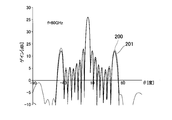
- FIG. 7 is a graph showing the total gain in the antenna device of the present embodiment.
- FIG. 8 is a graph showing the reflection loss (S11) in the antenna device of the present embodiment.
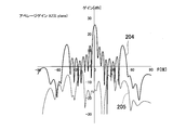
- FIG. 9 is a graph showing the average gain XZ (E plane) in the antenna device of the present embodiment.
- FIG. 10 is a graph showing the average gain YZ (H plane) in the antenna device of the present embodiment.
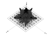
- FIG. 11 is a three-dimensional graph showing the gain of the antenna device of the present embodiment.
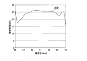
- FIG. 12 is a graph showing the total gain of the antenna device of the present embodiment.
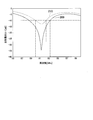
- FIG. 13 is a graph showing S11 of the slot portion of the antenna device of the present embodiment and S11 of the slot portion of the comparative example.
- FIG. 7 shows simulation results of all gains in the XZ plane and the YZ plane.
- the horizontal axis is the elevation angle ⁇ (degrees), and the vertical axis is the gain (dBi).
- a curve 200 (broken line) represents the total gain in the XZ plane
- a curve 201 (solid line) represents the total gain in the YZ plane.
- the XZ plane is an electric plane (E plane)
- the YZ plane is a magnetic plane (H plane).
- good overall gain is obtained in both the XZ plane and the YZ plane in the range of the elevation angle of 0 ° to ⁇ 4 °.
- FIG. 8 shows the frequency characteristics of the reflection loss (S11).
- the horizontal axis is frequency (GHz) and the vertical axis is reflection loss (dB).
- the reflection loss is ⁇ 10 dB or less in the range of about 56 GHz to about 64 GHz. For this reason, the antenna device 20 has a good return loss characteristic in a 60 GHz band wireless communication application.
- FIGS. 9 and 10 show simulation results of the average gain.
- FIG. 9 shows the average gain of the XZ plane
- FIG. 9 shows the average gain of the YZ plane.
- the horizontal axis is the elevation angle ⁇ (degrees)
- the vertical axis is the gain (dBi).
- curves 204 and 206 indicated by solid lines represent gains of co-polarization components
- curves 205 and 207 indicated by broken lines represent gains of cross-polarization components. According to FIGS. 9 and 10, almost the same average gain characteristics are obtained in both the XZ plane and the YZ plane. Therefore, there is no change in bidirectional gain.
- FIG. 11 shows a three-dimensional graph of the simulation result of the gain which is the basis of each of the graphs described above. Furthermore, FIG. 12 shows the total gain (dBi) in the frequency domain corresponding to FIG. According to a curve 208 in FIG. 12, a stable gain of about 25 dBi is obtained between about 58 GHz and about 64 GHz.
- FIG. 13 shows simulation results of the reflection loss S11 of the respective slot portions in the antenna device 20 of the embodiment and the antenna device 120 of the comparative example.
- the horizontal axis is frequency (GHz) and the vertical axis is reflection loss S11 (dB).
- a curve 209 (solid line) represents S11 of the slot portion of the antenna device 20
- a curve 210 (dashed line) represents S11 of the slot portion of the antenna device 120.
- the range in which S11 is ⁇ 10 dB or less is 58.8 GHz to 63.5 GHz in the curve 209, while it is 60 GHz to 62.5 GHz in the curve 210.
- the frequency band in which S11 is good is about twice in this embodiment as compared with the comparative example.
- the cause of this is that, in the antenna device 20 of the present embodiment, the slot 7 has an H-shaped opening shape including the second opening 7 b, while in the antenna device 120 of the comparative example, the slot 107 is rectangular. It is thought that there is.
- the reflection loss can be reduced even in the case of using the planar antenna of the electromagnetic coupling feeding system.
- FIG. 14 is a schematic view showing the configuration of the slot portion of the antenna device of the first modified example of the present embodiment.
- the antenna device 30 of the present modification includes a ground conductor plate 34 instead of the ground conductor plate 4 in the above embodiment.
- the ground conductor plate 34 is provided with slots 37 instead of the slots 7 in the above embodiment.
- the slot 37 has a substantially triangular (strictly trapezoidal) second opening 37b as viewed in the Z-axis direction, instead of the second opening 7b of the above embodiment.
- the width of the opening in the X-axis direction gradually widens from each end of the first opening 7a in the Y-axis direction as the distance from the center of the first opening 7a increases.
- the width in the X-axis direction of each second opening 37b is expanded from W2 to W33 (where W33> W2).
- the tip in the Y-axis direction in each of the second openings 37 b has a linear shape orthogonal to the central axis O.
- the shape of each second opening 37 b may be asymmetrical with respect to the central axis O, but in the present variation, as an example, the shape is axisymmetrical with respect to the central axis O.
- the second embodiment is substantially triangular as viewed from the Z-axis direction in the second opening 37b, and is not rectangular as in the second opening 7b of the slot 7 in the above embodiment. It is different from However, since the second opening 37b is wider in the X-axis direction than the width of the first opening 7a, like the second opening 7b, the second opening 37b has a higher impedance than the first opening 7a. It is an opening. For this reason, the antenna device 30 can optimize the coupling impedance of the electromagnetic coupling feeding portion as in the above embodiment, and can reduce the reflection loss even when using the planar antenna of the electromagnetic coupling feeding system.
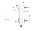
- FIG. 15 is a schematic view showing the configuration of the slot portion of the antenna device of the second modified example of the present embodiment.
- the antenna device 40 of the present modification includes a ground conductor plate 44 in place of the ground conductor plate 4 in the above embodiment. As shown in FIG. 15, the ground conductor plate 44 is provided with slots 47 instead of the slots 7 in the above embodiment.
- the ground conductor plate 44 is provided with slots 47 instead of the slots 7 in the above embodiment.
- the slot 47 includes a second opening 47b substantially circular (strictly speaking, an arc shape having a central angle larger than 180 °) as viewed from the Z-axis direction, instead of the second opening 7b of the above embodiment.
- the inner diameter of the second opening 47b is W43 (where W43> W2). Therefore, in the second opening 47b, the opening width in the X-axis direction becomes W43 as the distance from each end of the first opening 7a in the Y-axis direction to the center of the first opening 7a increases. The width gradually increases until it becomes smaller, and from there, the width gradually narrows as it goes away from the center of the first opening 7a.
- the antenna device 40 is different in that the second opening 47 b is substantially circular when viewed from the Z-axis direction, and is not rectangular as the second opening 7 b of the slot 7 in the above embodiment.
- the impedance of the second opening 47b is higher than that of the first opening 7a as in the second opening 7b. It is an opening.
- the antenna device 40 can optimize the coupling impedance of the electromagnetic coupling feeding portion as in the above embodiment, and can reduce the reflection loss even when using the planar antenna of the electromagnetic coupling feeding system.
- the second opening may have another shape as long as it is formed to be wider than the first opening from the connection with the first opening.
- the opening shape of the second opening may be a pentagon or more polygon, an oval, or the like.
- the opening shape of the second opening may be an opening shape in which the sides of an appropriate polygon are replaced with a concave or convex curve.
- the opening shape of the second opening is an opening shape including a widening portion widening from the first opening and a narrowing portion narrowing from the widening portion by a combination of various straight lines or curves. It is also good.
- the four radiating elements 1a are arranged in a rectangular grid having a substantially square grid to form the patch antenna 1, and the patch antenna 1 is further arranged in the square grid.
- the four radiation elements 1a may be arranged in a rectangular grid shape in which the arrangement pitch in the first direction and the second direction is largely different.
- the patch antenna 1 is not limited to the square lattice arrangement, and may be arranged in a rectangular lattice arrangement.
- the tip of the feeding conductor and the slot are orthogonal to each other as viewed in the normal direction, but the tip of the feeding conductor and the slot are in the normal direction.
- the crossing angles are not limited to right angles as long as they cross each other as seen from the figure.
- SYMBOLS 1 patch antenna, 1a ... radiation
Landscapes
- Waveguide Aerials (AREA)
- Variable-Direction Aerials And Aerial Arrays (AREA)
Abstract
La présente invention concerne un dispositif d'antenne qui comprend : une première couche diélectrique ; une antenne à plaque plane disposée sur une première surface de la première couche diélectrique et comprenant une section d'électrode pour un couplage électromagnétique ; une plaque de conducteur de terre disposée sur une seconde surface sur le côté opposé à la première surface dans la première couche diélectrique et comportant une fente formée à l'intérieur qui constitue une section non conductrice s'étendant dans une première direction et se trouvant dans une position faisant face à la section d'électrode ; une seconde couche diélectrique fixée à la plaque de conducteur de terre de manière à faire face à la première couche diélectrique ayant la plaque de conducteur de terre interposée entre elles ; et un conducteur d'alimentation électrique linéaire formé dans la seconde couche diélectrique de manière à faire face à la plaque de conducteur de terre ayant la seconde couche diélectrique interposée entre eux, dont la pointe s'étend dans une seconde direction croisant la première direction lorsqu'elle est observée depuis la direction normale de l'antenne à plaque, et qui est disposée selon une relation de position de manière à croiser la fente lorsqu'elle est observée depuis la direction normale. La fente comprend : une première ouverture ayant une première largeur constante dans la seconde direction ; et une seconde ouverture reliée aux deux extrémités de la première ouverture dans la première direction et qui est plus élargie que la première largeur, à proximité d'une section se raccordant à la première ouverture.
Applications Claiming Priority (2)
| Application Number | Priority Date | Filing Date | Title |
|---|---|---|---|
| JP2017181338A JP2019057831A (ja) | 2017-09-21 | 2017-09-21 | アンテナ装置 |
| JP2017-181338 | 2017-09-21 |
Publications (1)
| Publication Number | Publication Date |
|---|---|
| WO2019058932A1 true WO2019058932A1 (fr) | 2019-03-28 |
Family
ID=65810228
Family Applications (1)
| Application Number | Title | Priority Date | Filing Date |
|---|---|---|---|
| PCT/JP2018/032371 Ceased WO2019058932A1 (fr) | 2017-09-21 | 2018-08-31 | Dispositif d'antenne |
Country Status (2)
| Country | Link |
|---|---|
| JP (1) | JP2019057831A (fr) |
| WO (1) | WO2019058932A1 (fr) |
Families Citing this family (1)
| Publication number | Priority date | Publication date | Assignee | Title |
|---|---|---|---|---|
| WO2020262384A1 (fr) * | 2019-06-25 | 2020-12-30 | 京セラ株式会社 | Antenne, module de communication sans fil et dispositif de communication sans fil |
Citations (4)
| Publication number | Priority date | Publication date | Assignee | Title |
|---|---|---|---|---|
| JPH06232626A (ja) * | 1993-02-02 | 1994-08-19 | A T R Koudenpa Tsushin Kenkyusho:Kk | スロット結合型マイクロストリップアンテナ |
| JP2002033617A (ja) * | 2001-06-01 | 2002-01-31 | Mitsubishi Electric Corp | 給電装置 |
| JP2008048090A (ja) * | 2006-08-14 | 2008-02-28 | Ntt Docomo Inc | パッチアンテナ |
| JP2008306552A (ja) * | 2007-06-08 | 2008-12-18 | Fujikura Ltd | 透明アンテナ |
-
2017
- 2017-09-21 JP JP2017181338A patent/JP2019057831A/ja active Pending
-
2018
- 2018-08-31 WO PCT/JP2018/032371 patent/WO2019058932A1/fr not_active Ceased
Patent Citations (4)
| Publication number | Priority date | Publication date | Assignee | Title |
|---|---|---|---|---|
| JPH06232626A (ja) * | 1993-02-02 | 1994-08-19 | A T R Koudenpa Tsushin Kenkyusho:Kk | スロット結合型マイクロストリップアンテナ |
| JP2002033617A (ja) * | 2001-06-01 | 2002-01-31 | Mitsubishi Electric Corp | 給電装置 |
| JP2008048090A (ja) * | 2006-08-14 | 2008-02-28 | Ntt Docomo Inc | パッチアンテナ |
| JP2008306552A (ja) * | 2007-06-08 | 2008-12-18 | Fujikura Ltd | 透明アンテナ |
Also Published As
| Publication number | Publication date |
|---|---|
| JP2019057831A (ja) | 2019-04-11 |
Similar Documents
| Publication | Publication Date | Title |
|---|---|---|
| JP6129857B2 (ja) | 偏波共用アンテナ | |
| US9698487B2 (en) | Array antenna | |
| US7106256B2 (en) | Antenna device | |
| US8723751B2 (en) | Antenna system with planar dipole antennas and electronic apparatus having the same | |
| WO2017150054A1 (fr) | Antenne réseau | |
| US11223132B2 (en) | Antenna device | |
| CN115832689A (zh) | 一种宽波束毫米波圆极化磁电偶极子天线 | |
| US6091366A (en) | Microstrip type antenna device | |
| JP5523992B2 (ja) | 無指向性アンテナ装置及びアレーアンテナ装置 | |
| WO2016047779A1 (fr) | Réseau d'antennes, appareil de communication sans fil, et procédé de fabrication de réseau d'antennes | |
| JP5139919B2 (ja) | クロスダイポールアンテナ | |
| JP7721852B2 (ja) | パッチアンテナ | |
| CN106785404B (zh) | 一种新型嵌入式宽带双极化天线 | |
| CN106450777A (zh) | 圆极化微带天线 | |
| WO2019058932A1 (fr) | Dispositif d'antenne | |
| US11108166B2 (en) | Antenna device | |
| JP3764289B2 (ja) | マイクロストリップアンテナ | |
| JP7485452B2 (ja) | 広帯域無指向性アンテナ | |
| US12080943B2 (en) | Antenna module | |
| JP6398653B2 (ja) | パッチアンテナ | |
| KR20130087144A (ko) | 슬롯 안테나 장치 및 그 제공방법 | |
| JP6201651B2 (ja) | アンテナ装置およびアレイアンテナ装置 | |
| JP7608660B2 (ja) | アンテナ装置 | |
| JP7673655B2 (ja) | アンテナ装置 | |
| JP7359314B2 (ja) | アンテナ装置 |
Legal Events
| Date | Code | Title | Description |
|---|---|---|---|
| 121 | Ep: the epo has been informed by wipo that ep was designated in this application |
Ref document number: 18858393 Country of ref document: EP Kind code of ref document: A1 |
|
| NENP | Non-entry into the national phase |
Ref country code: DE |
|
| 122 | Ep: pct application non-entry in european phase |
Ref document number: 18858393 Country of ref document: EP Kind code of ref document: A1 |