WO2019059085A1 - Circuit de filtre et module haute fréquence - Google Patents
Circuit de filtre et module haute fréquence Download PDFInfo
- Publication number
- WO2019059085A1 WO2019059085A1 PCT/JP2018/033975 JP2018033975W WO2019059085A1 WO 2019059085 A1 WO2019059085 A1 WO 2019059085A1 JP 2018033975 W JP2018033975 W JP 2018033975W WO 2019059085 A1 WO2019059085 A1 WO 2019059085A1
- Authority
- WO
- WIPO (PCT)
- Prior art keywords
- band
- frequency band
- communication
- filter circuit
- signal
- Prior art date
- Legal status (The legal status is an assumption and is not a legal conclusion. Google has not performed a legal analysis and makes no representation as to the accuracy of the status listed.)
- Ceased
Links
Images


Classifications
-
- H—ELECTRICITY
- H04—ELECTRIC COMMUNICATION TECHNIQUE
- H04J—MULTIPLEX COMMUNICATION
- H04J1/00—Frequency-division multiplex systems
- H04J1/02—Details
- H04J1/04—Frequency-transposition arrangements
- H04J1/045—Filters applied to frequency transposition
-
- H—ELECTRICITY
- H04—ELECTRIC COMMUNICATION TECHNIQUE
- H04B—TRANSMISSION
- H04B1/00—Details of transmission systems, not covered by a single one of groups H04B3/00 - H04B13/00; Details of transmission systems not characterised by the medium used for transmission
- H04B1/005—Details of transmission systems, not covered by a single one of groups H04B3/00 - H04B13/00; Details of transmission systems not characterised by the medium used for transmission adapting radio receivers, transmitters andtransceivers for operation on two or more bands, i.e. frequency ranges
- H04B1/0053—Details of transmission systems, not covered by a single one of groups H04B3/00 - H04B13/00; Details of transmission systems not characterised by the medium used for transmission adapting radio receivers, transmitters andtransceivers for operation on two or more bands, i.e. frequency ranges with common antenna for more than one band
- H04B1/0057—Details of transmission systems, not covered by a single one of groups H04B3/00 - H04B13/00; Details of transmission systems not characterised by the medium used for transmission adapting radio receivers, transmitters andtransceivers for operation on two or more bands, i.e. frequency ranges with common antenna for more than one band using diplexing or multiplexing filters for selecting the desired band
-
- H—ELECTRICITY
- H03—ELECTRONIC CIRCUITRY
- H03K—PULSE TECHNIQUE
- H03K17/00—Electronic switching or gating, i.e. not by contact-making and –breaking
- H03K17/16—Modifications for eliminating interference voltages or currents
- H03K17/161—Modifications for eliminating interference voltages or currents in field-effect transistor switches
- H03K17/162—Modifications for eliminating interference voltages or currents in field-effect transistor switches without feedback from the output circuit to the control circuit
- H03K17/163—Soft switching
- H03K17/164—Soft switching using parallel switching arrangements
-
- H—ELECTRICITY
- H04—ELECTRIC COMMUNICATION TECHNIQUE
- H04B—TRANSMISSION
- H04B1/00—Details of transmission systems, not covered by a single one of groups H04B3/00 - H04B13/00; Details of transmission systems not characterised by the medium used for transmission
- H04B1/005—Details of transmission systems, not covered by a single one of groups H04B3/00 - H04B13/00; Details of transmission systems not characterised by the medium used for transmission adapting radio receivers, transmitters andtransceivers for operation on two or more bands, i.e. frequency ranges
- H04B1/0053—Details of transmission systems, not covered by a single one of groups H04B3/00 - H04B13/00; Details of transmission systems not characterised by the medium used for transmission adapting radio receivers, transmitters andtransceivers for operation on two or more bands, i.e. frequency ranges with common antenna for more than one band
- H04B1/006—Details of transmission systems, not covered by a single one of groups H04B3/00 - H04B13/00; Details of transmission systems not characterised by the medium used for transmission adapting radio receivers, transmitters andtransceivers for operation on two or more bands, i.e. frequency ranges with common antenna for more than one band using switches for selecting the desired band
-
- H—ELECTRICITY
- H04—ELECTRIC COMMUNICATION TECHNIQUE
- H04B—TRANSMISSION
- H04B1/00—Details of transmission systems, not covered by a single one of groups H04B3/00 - H04B13/00; Details of transmission systems not characterised by the medium used for transmission
- H04B1/38—Transceivers, i.e. devices in which transmitter and receiver form a structural unit and in which at least one part is used for functions of transmitting and receiving
- H04B1/40—Circuits
- H04B1/50—Circuits using different frequencies for the two directions of communication
- H04B1/52—Hybrid arrangements, i.e. arrangements for transition from single-path two-direction transmission to single-direction transmission on each of two paths or vice versa
-
- H—ELECTRICITY
- H04—ELECTRIC COMMUNICATION TECHNIQUE
- H04B—TRANSMISSION
- H04B1/00—Details of transmission systems, not covered by a single one of groups H04B3/00 - H04B13/00; Details of transmission systems not characterised by the medium used for transmission
- H04B1/38—Transceivers, i.e. devices in which transmitter and receiver form a structural unit and in which at least one part is used for functions of transmitting and receiving
- H04B1/40—Circuits
- H04B1/54—Circuits using the same frequency for two directions of communication
- H04B1/56—Circuits using the same frequency for two directions of communication with provision for simultaneous communication in two directions
-
- H—ELECTRICITY
- H03—ELECTRONIC CIRCUITRY
- H03D—DEMODULATION OR TRANSFERENCE OF MODULATION FROM ONE CARRIER TO ANOTHER
- H03D2200/00—Indexing scheme relating to details of demodulation or transference of modulation from one carrier to another covered by H03D
- H03D2200/0041—Functional aspects of demodulators
- H03D2200/0054—Digital filters
- H03D2200/0058—Digital filters using a digital filter with interpolation
Definitions
- the present invention relates to a filter circuit and a high frequency module, and more particularly to a filter circuit and a high frequency module for performing multi-band communication using a plurality of frequency bands.
- E-UTRA Evolved Universal Terrestrial Radio Access
- 3GPP 3rd Generation Partnership Project
- LTE Long Term Evolution
- a frequency band is defined for each of a plurality of communication bands used in multiband communication.
- Patent Document 1 discloses a multiband front end circuit including a filter circuit that processes signals in a plurality of communication bands.
- the filter circuit shown in FIG. 5 of Patent Document 1 processes the signals of bands 7, 38 and 40 in E-UTRA.
- an object of this invention is to provide the high frequency module provided with the filter circuit which an apparatus does not enlarge easily even if a communication band increases, and such a filter circuit.
- a filter circuit includes a first common terminal, a first selected terminal, and a second selected terminal, and the first common terminal and the first target are provided.
- a first switch circuit exclusively connecting one of the selection terminal and the second selected terminal, and a first frequency band connected to the first selected terminal, which is a frequency band of a first communication band
- a frequency band of a second communication band connected to a first signal terminal for transmitting a first communication signal to which the second communication signal belongs, and the second selected terminal and used exclusively with the first communication band
- a second signal terminal for transmitting a second communication signal belonging to a second frequency band at least partially overlapping the frequency band, and one end connected to the first common terminal, the first frequency band and the second Passband with both frequency bands Comprising a first band-pass filter that, the.
- the first communication signal of the first communication band and the second communication signal of the second communication band are filtered by a single first band pass filter.
- the required number of filters is reduced as compared to the case where the first communication signal and the second communication signal are filtered by separate filters, so that a filter circuit which is difficult to increase in size even when the communication band increases.
- a high frequency module comprising such a filter circuit is obtained.
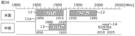
- FIG. 1A is a diagram showing an example of a frequency band of a communication band.
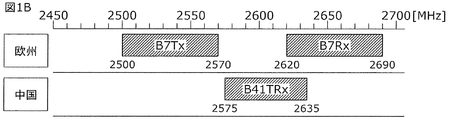
- FIG. 1B is a diagram showing an example of a frequency band of the communication band.
- FIG. 2 is a block diagram showing an example of a functional configuration of a filter circuit according to a reference example.
- FIG. 3A is a diagram illustrating an example of a pass band of a filter.
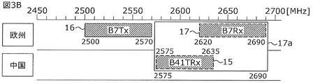
- FIG. 3B is a diagram illustrating an example of the pass band of the filter.
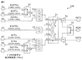
- FIG. 4 is a block diagram showing an example of a functional configuration of the filter circuit according to the first embodiment.
- FIG. 5 is a diagram illustrating another example of the pass band of the filter.
- FIG. 6A is a block diagram showing an example of a functional configuration of the high frequency module according to the second embodiment.
- FIG. 6B is a block diagram showing an example of a functional configuration of the high frequency module according to the second embodiment.
- FIG. 6C is a block diagram showing an example of a functional configuration of the high frequency module
- the filter circuit according to the first embodiment is a filter circuit for performing multi-band communication using a plurality of communication bands.
- a filter circuit for performing multiband communication in five communication bands of bands 7, 25, 34, 39, and 41 defined by E-UTRA will be described.
- the five communication bands include a communication band in which duplex mode is FDD (Frequency Division Duplex) and a communication band in which duplex mode is TDD (Time Division Duplex).
- FDD Frequency Division Duplex
- TDD Time Division Duplex
- FDD Frequency Division Duplex
- TDD Time Division Duplex
- FDD Frequency Division Duplex
- TDD Time Division Duplex
- Band 7 has a duplex mode of FDD and is operated in Europe.
- the transmission frequency band B7Tx of band 7 is from 2500 MHz to 2570 MHz, and the reception frequency band B7Rx of band 7 is from 2620 MHz to 2690 MHz.
- Band 25 has a duplex mode of FDD and is operated in the United States.
- the transmission frequency band B25Tx of band 25 is from 1850 MHz to 1915 MHz, and the reception frequency band B25 Rx of band 25 is from 1930 MHz to 1995 MHz.
- Band 34 is duplex mode TDD and is operated in China.
- the transmission and reception frequency band B34TRx of the band 34 is from 2010 MHz to 2025 MHz.
- Band 39 is a duplex mode TDD and is operated in China.
- the transmission and reception frequency band B39TRx of the band 39 is from 1880 MHz to 1920 MHz.
- Band 41 is in duplex mode TDD and is operated in China.
- the transmission and reception frequency band B41TRx of the band 41 is from 2575 MHz to 2635 MHz.
- the band 41 of the entire band of the band 41 defined by E-UTRA, only the range operated by a specific communication carrier in China is described.
- a filter circuit for performing multi-band communication is configured of a duplexer provided for each duplex communication band of FDD and a multiplexer including a filter provided for each duplex communication band of duplex mode. Be done.
- the duplexer demultiplexes and combines the transmit signal and the receive signal of the corresponding FDD communication band, and the multiplexer demultiplexes and combines the transmit / receive signal of each TDD communication band.
- the filter circuit of Patent Document 1 described above also has such a configuration.
- a filter circuit for performing multiband communication in five communication bands of bands 7, 25, 34, 39, and 41 a reference example having such a configuration can be considered.
- FIG. 2 is a block diagram showing an example of a functional configuration of a filter circuit according to a reference example.
- the filter circuit 900 shown in FIG. 2 includes signal terminals P1 to P7, filters 11 to 17, switches 21 and 33, directional couplers 31 and 32, antenna terminals ANT1 and ANT2, and a monitor terminal MON.
- the filters 11 and 12 are band pass filters respectively having the transmission frequency band B25Tx and the reception frequency band B25Rx of the band 25 as pass bands, and one end is connected to each of the signal terminals P2 and P4 and the other end is connected to each other .
- the filters 11 and 12 constitute a duplexer that demultiplexes and combines the transmit signal and the receive signal of the band 25.
- the filters 13, 14, 15 are band pass filters respectively having the transmission / reception frequency bands B39TRx, B34TRx, B41TRx of the bands 39, 34, 41 as pass bands, one end of which is connected to the signal terminals P1, P3, P5, The ends are connected to one another.
- the filters 13, 14, 15 constitute a triplexer that demultiplexes and combines the transmission and reception signals of the bands 39, 34, 41.
- the filters 16 and 17 are band pass filters respectively having the transmission frequency band B7Tx and the reception frequency band B7Rx of the band 7 as pass bands, one end thereof being connected to the signal terminals P7 and P6 respectively, and the other end being mutually connected .
- the filters 16 and 17 constitute a duplexer that demultiplexes and combines the transmission signal and the reception signal of the band 7.
- the switch 21 has common terminals C10 and C11 to be connected to the antenna, and a plurality of selected terminals S11 to S15 selectively connected to the common terminals C10 and C11.
- the non-selection terminal S11 of the switch 21 is connected to the duplexer constituted by the filters 11 and 12.
- the non-selection terminal S12 of the switch 21 is connected to a triplexer constituted by the filters 13, 14, 15.
- the non-selection terminal S13 of the switch 21 is connected to a duplexer constituted by the filters 16 and 17.
- the common terminals C10 and C11 of the switch 21 are connected to the antenna terminals ANT1 and ANT2 through the directional couplers 31 and 32, respectively.
- the directional coupler 31 is provided on a signal path connecting the common terminal C10 and the antenna terminal ANT1, and outputs a detection signal according to the size of the transmission signal flowing through the signal path.
- the directional coupler 32 is provided on a signal path connecting the common terminal C11 and the antenna terminal ANT2, and outputs a detection signal according to the size of the transmission signal flowing through the signal path.
- the switch 33 selectively transmits one of the detection signals output from the directional couplers 31 and 32 to the monitor terminal MON.
- filter circuit 900 For convenience of explanation, although five communication bands are illustrated in filter circuit 900, for example, as dozens of communication bands are defined in E-UTRA, a practical filter circuit corresponds to more communication bands. There is a need. In the filter circuit for performing multi-mode communication in accordance with communication standards other than E-UTRA, it is considered that the communication band to be supported will be further increased.
- the filter circuit 900 if two filters are provided for each FDD communication band and one filter is provided for each TDD communication band, a large number of filters are required, and the size of the device increases. Is inevitable.
- FIG. 3A and FIG. 3B are diagrams showing an example of the pass band of the filter.
- FIGS. 3A and 3B specifically show the passbands of the filters corresponding to the respective communication bands shown in FIGS. 1A and 1B.
- signals of a plurality of communication bands in which at least a part of frequency bands overlap and are not simultaneously communicated are filtered by one filter.
- band 25 and band 39 are operated in the United States and China, respectively, and are examples of communication bands used exclusively in different regions.
- the frequency band from 1850 MHz to 1920 MHz including the transmission frequency band B25Tx of band 25 and the transmission / reception frequency band B39TRx of band 39 does not include other communication bands in any of the United States and China.
- the transmission of band 25 is performed using filter 11a, which uses the frequency band from 1850 MHz to 1920 MHz as the pass band (that is, the transmission frequency band B25Tx of band 25 and the transmission / reception frequency band B39TRx of band 39 as the pass band). Filter both the signal and the band 39 transmit and receive signals.
- band 7 and band 41 are respectively operated in Europe and China, and are examples of communication bands used exclusively in different regions.
- the frequency band from 2575 MHz to 2690 MHz including the reception frequency band B7Rx of band 7 and the transmission / reception frequency band B41TRx of band 41 does not include any other communication band in any of Europe and China.
- the filter circuit according to the first embodiment is configured as follows.
- FIG. 4 is a block diagram showing an example of a functional configuration of the filter circuit according to the first embodiment.
- the filter circuit 100 shown in FIG. 4 differs from the filter circuit 900 in FIG. 2 in that the filters 11 and 17 are replaced by the filters 11a and 17a, the filters 13 and 15 are eliminated, and the switches 22 and 23 respectively. The difference is in that
- the switch 22 has selected terminals S21 and S22 exclusively connected to the common terminal C20 and the common terminal C20.
- the signal terminal P1 is connected to the selected terminal S21, and transmits the transmission / reception signal of the band 39.
- the signal terminal P2 is connected to the selected terminal S22, and transmits the transmission signal of the band 25.
- the transmission and reception frequency band B39TRx of the band 39 and the transmission frequency band B25Tx of the band 25 at least partially overlap.
- the filter 11a is a band pass filter that passes both of the transmission / reception frequency band B39TRx of the band 39 and the transmission frequency band B25Tx of the band 25 as a pass band, and one end thereof is connected to the common terminal C20.
- the band 39 is an example of the first communication band
- the transmission / reception frequency band B39TRx of the band 39 is an example of the first frequency band.
- the band 25 is an example of a second communication band
- the transmission frequency band B25Tx of the band 25 is an example of a second frequency band.
- the transmission and reception signal of band 39 and the transmission signal of band 25 are examples of the first communication signal and the second communication signal, respectively.
- the signal terminals P1 and P2 are an example of a first signal terminal and a second signal terminal, respectively.
- the switch 22 is an example of a first switch circuit
- the common terminal C20 and the non-selection terminals S21 and S22 are examples of a first common terminal, a first selected terminal, and a second selected terminal, respectively.
- the filter 11a is an example of a first band pass filter.
- the signal terminal P3 transmits the transmission / reception signal of the band 34.
- the transmission / reception frequency band B34TRx of the band 34 and the transmission / reception frequency band B39TRx of the band 39 do not overlap.
- the filter 14 is a band pass filter having a transmission / reception frequency band B34TRx of the band 34 as a pass band, and one end thereof is connected to the signal terminal P3.
- the band 34 is an example of the third communication band
- the transmission / reception frequency band B34TRx of the band 34 is an example of the third frequency band
- the transmission / reception signal of the band 34 is an example of the third communication signal.
- the signal terminal P3 is an example of a third signal terminal
- the filter 14 is an example of a second band pass filter.
- the signal terminal P4 transmits the band 25 received signal.
- the transmission frequency band B25Tx of the band 25 and the reception frequency band B25Rx do not overlap.
- the filter 12 is a band pass filter that uses the reception frequency band B25Rx of the band 25 as a pass band, and one end thereof is connected to the signal terminal P4.
- the other end of the filter 11 a and the other end of the filter 12 are connected to each other to constitute a duplexer for the band 25.
- the reception frequency band B25Rx of the band 25 is an example of the fourth frequency band
- the reception signal of the band 25 is an example of the fourth communication signal.
- the signal terminal P4 is an example of a fourth signal terminal
- the filter 12 is an example of a third band pass filter.
- the switch 23 has selected terminals S31 and S32 which are exclusively connected to the common terminal C30 and the common terminal C30.
- the signal terminal P5 is connected to the selected terminal S31, and transmits the transmission / reception signal of the band 41.
- the signal terminal P6 is connected to the selected terminal S32, and transmits the band 7 reception signal.
- the transmission / reception frequency band B41TRx of the band 41 and the reception frequency band B7Rx of the band 7 at least partially overlap, and the transmission / reception frequency band B41TRx of the band 41, the transmission / reception frequency band B34TRx of the band 34, and the transmission / reception frequency band B39TRx of the band 39 None overlap.
- the filter 17a is a band pass filter that passes both of the transmission / reception frequency band B41TRx of the band 41 and the reception frequency band B7Rx of the band 7 as a pass band, and one end thereof is connected to the common terminal C30.
- the band 41 is an example of a fourth communication band
- the transmission / reception frequency band B41TRx of the band 41 is an example of a fifth frequency band
- the band 7 is an example of a fifth communication band
- the reception frequency band B7Rx of the band 7 is an example of a sixth frequency band.
- the transmission and reception signal of band 41 and the reception signal of band 7 are examples of the fifth communication signal and the sixth communication signal, respectively.
- the signal terminals P5 and P6 are an example of a fifth signal terminal and a sixth signal terminal, respectively.
- the switch 23 is an example of a second switch circuit
- the common terminal C30 and the non-selection terminals S31 and S32 are examples of a second common terminal, a third selected terminal, and a fourth selected terminal, respectively.
- the filter 17a is an example of a fourth band pass filter.
- the signal terminal P7 transmits the band 7 transmission signal.
- the transmission frequency band B7Tx of the band 7 and the reception frequency band B7Rx do not overlap.
- the filter 16 is a band pass filter having a transmission frequency band B7Tx of the band 7 as a pass band, and one end thereof is connected to the signal terminal P7.
- the other end of the filter 16 and the other end of the filter 17a are connected to each other to constitute a duplexer for the band 7.
- the transmission frequency band B7Tx of the band 7 is an example of the seventh frequency band
- the transmission signal of the band 7 is an example of the seventh communication signal.
- the signal terminal P7 is an example of a seventh signal terminal
- the filter 16 is an example of a fifth band pass filter.
- the transmission and reception signal of the band 39 is filtered using the filter 11a which is also the transmission filter of the duplexer for the band 25.
- one of the reception signal of the band 7 and the transmission and reception signal of the band 41, which is exclusively selected by the switch 23, is filtered by the filter 17a.
- the transmission / reception signal of the band 41 is filtered using the filter 17a which is also the reception filter of the duplexer for the band 7.
- the following effects can be obtained as compared with the filter circuit 900 of FIG.
- the filter circuit 900 demultiplexes the transmit signal and the receive signal of the band 25 and band 7 in duplex mode with FDD by the duplexer consisting of the filters 11 and 12, and the duplexer consisting of the filters 16 and 17, respectively. And combined. Further, transmission and reception signals of band 39, band 34 and band 41 in duplex mode TDD are demultiplexed and multiplexed by a multiplexer consisting of filters 13, 14 and 15 for each communication band.
- the transmit signal and receive signal in the communication band of duplex mode FDD and the transmit and receive signals in the communication band in duplex mode TDD are respectively processed by separate filters included in the duplexer and multiplexer. Ru.
- the filter 11 is replaced with the filter 11a whose passband is broadened so as to include the passbands of both the filter 13 and the filter 11.
- the filter 17 is replaced with a filter 17a whose passband is broadened so as to include the passbands of both the filter 15 and the filter 17.
- filter circuit 100 while requiring multiband communication in five communication bands of bands 7, 25, 34, 39, and 41, the required number of filters is two as compared with filter circuit 900. Will be reduced.
- the signal of the FDD communication band and the signal of the TDD communication band are processed by separate filters as in the filter circuit 900 of FIG.
- the pass band of the filter for the FDD communication band is made to include the pass band of the filter for the TDD communication band While expanding, added a switch to perform exclusive control. This makes it possible to miniaturize the device by processing the FDD communication band and the TDD communication band with the same single filter.
- the switch 21 shown in FIG. 4 is not essential. Since any of the pass bands of the filters 11a, 12, 14, 16, 17a do not overlap with each other, all the other ends of the filters 11a, 12, 14, 16, 17a may be connected to form a multiplexer ( Not shown). In that case, the switch 21 is eliminated to obtain a filter circuit having a single antenna terminal. In such a filter circuit, as in the filter 100, it is possible to reduce the required number of filters.
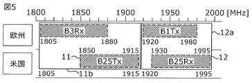
- FIG. 5 is a diagram illustrating another example of the pass band of the filter.
- Band 3 and Band 25 are operated in Europe and the United States respectively, and are examples of communication bands used exclusively in different regions.
- the frequency band from 1805 MHz to 1915 MHz including the band 3 reception frequency band B3Rx and the band 25 transmission frequency band B25Tx does not include any other communication band in any of Europe and the United States.
- both the receive signal of band 3 and the transmit signal of band 25 are used.
- Band 1 and Band 25 are operated in Europe and the United States respectively, and are examples of communication bands used exclusively in different regions.
- the frequency band from 1920 MHz to 1995 MHz including the band 1 transmission frequency band B1Tx and the band 25 reception frequency band B25Rx does not include any other communication band in any of Europe and the United States.
- transmission of band 1 is performed using filter 12a that sets the frequency band from 1920 MHz to 1995 MHz as the pass band (that is, sets both transmission frequency band B1 Tx of band 1 and reception frequency band B25 Rx of band 25 as the pass band). Filter both the signal and the received signal of band 25.
- the reception signal of band 3 and the transmission signal of band 25 are filtered by the same filter 11 b. Also, the transmission signal of band 1 and the reception signal of band 25 are filtered by the same filter 12a. This reduces the required number of filters by two and suppresses the increase in size of the device.
- the high frequency module according to the second embodiment includes the filter circuit according to the first embodiment, and an example of the high frequency module supporting carrier aggregation communication in which communication is performed using two communication bands simultaneously is given.
- the filter circuit according to the first embodiment includes the filter circuit according to the first embodiment, and an example of the high frequency module supporting carrier aggregation communication in which communication is performed using two communication bands simultaneously is given.
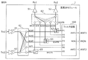
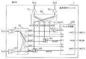
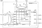
- FIGS. 6A, 6B and 6C are block diagrams showing an example of a functional configuration of the high frequency module according to the second embodiment, and show different connection states of the same high frequency module.
- the high frequency module 1 includes power amplifiers 41 and 42, low noise amplifiers 51 and 52, switches 61 to 65, and a filter circuit 100.
- the filter circuit 100 is the filter circuit 100 shown in FIG.
- the switch 61 switches the connection between the output end of each of the power amplifiers 41 and 42 and any one of the transmission signal paths B39T, B25T, B34T, B7T, and B41T provided for each communication band.
- the switch 62 switches the connection between each input terminal of the low noise amplifiers 51 and 52 and any one of the reception signal paths B39R, B25R, B34R, B7R, and B41R provided for each communication band.
- the switch 63 switches the connection between the transmission / reception signal path B39TR provided in the band 39 and any one of the transmission signal path B39T and the reception signal path B39R.
- the switch 64 switches the connection between the transmission / reception signal path B34TR provided in the band 34 and any one of the transmission signal path B34T and the reception signal path B34R.
- the switch 65 switches the connection between the transmission / reception signal path B41TR provided in the band 41 and any one of the transmission signal path B41T and the reception signal path B41R.
- the switches 61 to 65 constitute a switch network.
- the switch network operates in one mode selected from at least a first mode, a second mode and a third mode according to a control signal not shown.
- signal paths connected in the first mode, the second mode and the third mode are indicated by thick lines.
- the switch network switches the connection between the signal terminal P3 of the filter circuit 100 and the power amplifier 41 or the low noise amplifier 51, and switches the connection between the signal terminal P1 and the power amplifier 42 or the low noise amplifier 52 (FIG. 6A). ).
- the transmission signal and the reception signal of the band 34 are respectively amplified by the power amplifier 41 and the low noise amplifier 51, and in parallel with this, the transmission signal and the reception signal of the band 39 are respectively amplified by the power amplifier 42 and the low noise amplifier 52. It is amplified. As a result, carrier aggregation by the bands 34 and 39 is performed in the first mode.
- the switch network switches the connection between the signal terminal P3 of the filter circuit 100 and the power amplifier 41 or the low noise amplifier 51, and switches the connection between the signal terminal P5 and the power amplifier 42 or the low noise amplifier 52 (FIG. 6B). ).
- the transmission signal and the reception signal of the band 34 are respectively amplified by the power amplifier 41 and the low noise amplifier 51, and in parallel with this, the transmission signal and the reception signal of the band 41 are respectively amplified by the power amplifier 42 and the low noise amplifier 52. It is amplified. As a result, carrier aggregation by the bands 34 and 41 is performed in the second mode.
- the switch network switches the connection between the signal terminal P1 of the filter circuit 100 and the power amplifier 41 or the low noise amplifier 51, and switches the connection between the signal terminal P5 and the power amplifier 42 or the low noise amplifier 52 (FIG. 6C). ).
- the transmission signal and the reception signal of band 39 are respectively amplified by power amplifier 41 and low noise amplifier 51, and in parallel with this, the transmission signal and the reception signal of band 41 are respectively amplified by power amplifier 42 and low noise amplifier 52. It is amplified. As a result, carrier aggregation by the bands 39 and 41 is performed in the third mode.
- carrier aggregation communication can be performed by three combinations of the band 34 and the band 39 in the first mode, the band 34 and the band 41 in the second mode, and the band 39 and the band 41 in the third mode A high frequency module 1 is obtained. Further, as described in the first embodiment, since the filter circuit 100 is used, the effect of suppressing the enlargement of the device can also be obtained.
- a filter circuit includes a first common terminal, a first selected terminal, and a second selected terminal, and the first common terminal, the first selected terminal, and the second selected terminal.
- a first switch circuit exclusively connected to any one of the terminals and a first communication signal connected to the first selected terminal and belonging to a first frequency band which is a frequency band of a first communication band are transmitted
- a second signal terminal for transmitting a second communication signal belonging to a second frequency band, and one end is connected to the first common terminal, and both the first frequency band and the second frequency band are pass bands
- the first communication signal of the first communication band and the second communication signal of the second communication band are filtered by a single first band pass filter.
- the required number of filters is reduced as compared to the case where the first communication signal and the second communication signal are filtered by different filters, so that a filter circuit which does not easily increase the size of the device even when the communication band increases is obtained.
- the duplex mode of the first communication band may be time division duplex, and the duplex mode of the second communication band may be frequency division duplex.
- the filter circuit is a third signal terminal for transmitting a third communication signal belonging to a third frequency band which is a frequency band of the third communication band and does not overlap the first frequency band, and one end thereof is the third signal terminal.
- a second band pass filter connected to three signal terminals and having the third frequency band as a pass band.
- the filter for the first communication signal included in the multiplexer can be replaced with a single first band pass filter that filters the first communication signal and the second communication signal.
- the second communication band has a transmission frequency band and a reception frequency band that do not overlap with each other, and the second frequency band is one of the transmission frequency band and the reception frequency band of the second communication band.
- the filter circuit includes: a fourth signal terminal for transmitting a fourth communication signal belonging to a fourth frequency band which is the other of the transmission frequency band and the reception frequency band of the second communication band; And a third band pass filter connected to the four signal terminals and having the fourth frequency band as a pass band.
- first band pass filter and the third band pass filter may be connected to each other to constitute a multiplexer.
- the first band pass filter and the third band pass filter are one and the other of the transmission filter and the reception filter for the second communication band, and the multiplexer functions as a duplexer for the second communication band . That is, the first communication signal is filtered using the transmission filter or the reception filter of the duplexer for the second communication band. As a result, the required number of filters is reduced, so that it is possible to obtain a filter circuit which does not easily increase in size even when the communication band is increased.
- the filter circuit has a second common terminal, a third selected terminal, and a fourth selected terminal, and any one of the second common terminal, the third selected terminal, and the fourth selected terminal.
- a second switch circuit for exclusively connecting one with the other, and a fifth for transmitting a fifth communication signal connected to the third selected terminal and belonging to a fifth frequency band that is a frequency band of the fourth communication band
- a sixth frequency that is connected to the signal terminal and the fourth selected terminal, and is a frequency band of a fifth communication band used exclusively with the fourth communication band, and at least a portion of which overlaps the fifth frequency band
- the fifth communication signal of the fourth communication band and the sixth communication signal of the fifth communication band are filtered by the single fourth band pass filter.
- the required number of filters is reduced as compared to the case where the fifth communication signal and the sixth communication signal are filtered by separate filters, so that a filter circuit which does not easily increase the size of the device even when the communication band increases is obtained.
- the duplex mode of the fourth communication band may be time division duplex, and the duplex mode of the fifth communication band may be frequency division duplex.
- the fifth frequency band may not overlap with any of the third frequency band and the one frequency band.
- the fifth communication signal, the third communication signal, and the first communication signal whose frequency bands do not overlap are generally demultiplexed and multiplexed by a multiplexer including a filter for each communication signal.
- the filter for the fifth communication signal included in the multiplexer can be replaced with a single fourth band pass filter that filters the fifth communication signal and the sixth communication signal. .
- the required number of filters is reduced, it is possible to obtain a filter circuit which does not easily increase in size even when the communication band is increased.
- the fifth communication band has a transmission frequency band and a reception frequency band that do not overlap each other, and the sixth frequency band is one of the transmission frequency band and the reception frequency band of the fifth communication band.
- the filter circuit includes a seventh signal terminal for transmitting a seventh communication signal belonging to a seventh frequency band that is the other of the transmission frequency band and the reception frequency band of the fifth communication band; And a fifth band pass filter connected to the seven signal terminals and having the seventh frequency band as a pass band.
- the fourth band pass filter and the fifth band pass filter may be connected to each other to form a multiplexer.
- the fourth band pass filter and the fifth band pass filter are one and the other of the transmission filter and the reception filter for the fifth communication band
- the multiplexer is a duplexer for the fifth communication band. That is, the sixth communication signal is filtered using the transmission filter or the reception filter that constitutes the duplexer for the fifth communication band.
- the first frequency band is a frequency band from 1880 MHz to 1920 MHz which is a transmission / reception frequency band of Band 39 in E-UTRA
- the second frequency band is a transmission frequency band 1850 MHz from Band 25 in E-UTRA. It may be a frequency band up to 1915 MHz.
- the third frequency band may be a frequency band from 2010 MHz to 2025 MHz, which is a transmission / reception frequency band of Band 34 in E-UTRA.
- the fourth frequency band may be a frequency band from 1930 MHz to 1995 MHz, which is a reception frequency band of Band 25 in E-UTRA.
- the fifth frequency band is a frequency band from 2575 MHz to 2635 MHz which is a part of the transmission and reception frequency band of Band 41 in E-UTRA
- the sixth frequency band is a reception frequency band of Band 7 in E-UTRA. It may be a certain frequency band from 2620 MHz to 2690 MHz.
- the seventh frequency band may be a frequency band from 2500 MHz to 2570 MHz, which is a transmission frequency band of Band 7 in E-UTRA.
- the first frequency band is a frequency band from 1805 MHz to 1880 MHz which is a reception frequency band of Band 3 in E-UTRA
- the second frequency band is a transmission frequency band from 1850 MHz which is Band 25 in E-UTRA. It may be a frequency band up to 1915 MHz.
- the first frequency band is a frequency band from 1920 MHz to 1980 MHz which is a transmission frequency band of Band 1 in E-UTRA
- the second frequency band is 1930 MHz which is a reception frequency band of Band 25 in E-UTRA. It may be a frequency band up to 1995 MHz.
- the filter circuit having the above-described effect can be applied to a specific communication band in E-UTRA.
- a high frequency module includes the filter circuit, and a power amplifier and a low noise amplifier electrically connected to the filter circuit.
- the one or more power amplifiers include a first power amplifier and a second power amplifier
- the one or more low noise amplifiers include a first low noise amplifier and a second low noise amplifier
- the filter circuit A switch network is provided between the first power amplifier, the second power amplifier, the first low noise amplifier, and the second low noise amplifier, and the switch network includes at least a first mode, a second mode, and a third mode.
- connection between the third signal terminal of the filter circuit and the first power amplifier or the first low noise amplifier in the first mode, and the first mode of the filter circuit A signal terminal and the second power amplifier or the second low
- the connection with the amplifier is switched, and in the second mode, the connection between the third signal terminal of the filter circuit and the first power amplifier or the first low noise amplifier is switched, and the fifth signal terminal of the filter circuit
- the connection with the second power amplifier or the second low noise amplifier is switched, and in the third mode, the connection between the first signal terminal of the filter circuit and one of the first power amplifier or the first low noise amplifier is selected. While switching, the connection between the fifth signal terminal of the filter circuit and the second power amplifier or the second low noise amplifier may be switched.
- the first communication band and the third communication band in the first mode, the third communication band and the fourth communication band in the second mode, the first communication band and the fourth communication band in the third mode, A high frequency module capable of carrier aggregation communication can be obtained by the three combinations of the above.
- the filter circuit and the high frequency module according to the embodiments of the present invention have been described above, the present invention is not limited to the individual embodiments. Without departing from the spirit of the present invention, various modifications that can be conceived by a person skilled in the art may be applied to the present embodiment, or a form constructed by combining components in different embodiments may be one or more of the present invention. It may be included within the scope of the embodiments.
- the present invention can be widely used in various communication devices as a filter circuit and a high frequency module.
Landscapes
- Engineering & Computer Science (AREA)
- Computer Networks & Wireless Communication (AREA)
- Signal Processing (AREA)
- Physics & Mathematics (AREA)
- Electromagnetism (AREA)
- Transceivers (AREA)
Abstract
L'invention concerne un circuit de filtre (100) qui comprend : un premier circuit de commutation (22) qui connecte un premier terminal commun (C20) avec exclusivement soit un premier terminal d'option de sélection (S21) soit un second terminal d'option de sélection (S22) ; un premier terminal de signal (P1) qui est connecté au premier terminal d'option de sélection (S21) et qui est destiné à transmettre un premier signal de communication appartenant à une première bande de fréquence (B39TRx) qui est une bande de fréquence d'une première bande de communication ; un second terminal de signal (P2) qui est connecté au second terminal d'option de sélection (S22) et qui est destiné à transmettre un second signal de communication appartenant à une seconde bande de fréquence (B25Tx) qui est une bande de fréquence d'une seconde bande de communication et qui chevauche au moins partiellement la première bande de fréquence (B39TRx) ; et un premier filtre passe-bande (11a) qui comporte une extrémité connectée au premier terminal commun (C20) et qui passe à la fois de la première bande de fréquence (B39TRx) et de la seconde bande de fréquence (B25Tx).
Priority Applications (2)
| Application Number | Priority Date | Filing Date | Title |
|---|---|---|---|
| CN201890001212.3U CN211702017U (zh) | 2017-09-21 | 2018-09-13 | 滤波电路和高频模块 |
| US16/822,838 US11323193B2 (en) | 2017-09-21 | 2020-03-18 | Filter circuit and radio-frequency module |
Applications Claiming Priority (2)
| Application Number | Priority Date | Filing Date | Title |
|---|---|---|---|
| JP2017-181571 | 2017-09-21 | ||
| JP2017181571 | 2017-09-21 |
Related Child Applications (1)
| Application Number | Title | Priority Date | Filing Date |
|---|---|---|---|
| US16/822,838 Continuation US11323193B2 (en) | 2017-09-21 | 2020-03-18 | Filter circuit and radio-frequency module |
Publications (1)
| Publication Number | Publication Date |
|---|---|
| WO2019059085A1 true WO2019059085A1 (fr) | 2019-03-28 |
Family
ID=65810820
Family Applications (1)
| Application Number | Title | Priority Date | Filing Date |
|---|---|---|---|
| PCT/JP2018/033975 Ceased WO2019059085A1 (fr) | 2017-09-21 | 2018-09-13 | Circuit de filtre et module haute fréquence |
Country Status (3)
| Country | Link |
|---|---|
| US (1) | US11323193B2 (fr) |
| CN (1) | CN211702017U (fr) |
| WO (1) | WO2019059085A1 (fr) |
Cited By (3)
| Publication number | Priority date | Publication date | Assignee | Title |
|---|---|---|---|---|
| WO2020202891A1 (fr) * | 2019-03-29 | 2020-10-08 | 株式会社村田製作所 | Module haute fréquence et dispositif de communication |
| WO2023203859A1 (fr) * | 2022-04-22 | 2023-10-26 | 株式会社村田製作所 | Circuit haute fréquence et appareil de communication |
| US12407373B2 (en) | 2020-08-28 | 2025-09-02 | Murata Manufacturing Co., Ltd. | Acoustic wave filter circuit, multiplexer, front-end circuit, and communication apparatus |
Families Citing this family (6)
| Publication number | Priority date | Publication date | Assignee | Title |
|---|---|---|---|---|
| JP2020170919A (ja) * | 2019-04-02 | 2020-10-15 | 株式会社村田製作所 | 高周波信号送受信回路 |
| WO2020226090A1 (fr) * | 2019-05-09 | 2020-11-12 | ソニーセミコンダクタソリューションズ株式会社 | Puce à semi-conducteur et dispositif de réception |
| JP2022083835A (ja) * | 2020-11-25 | 2022-06-06 | 株式会社村田製作所 | 高周波モジュール及び通信装置 |
| US20230144780A1 (en) * | 2021-11-08 | 2023-05-11 | Skyworks Solutions, Inc. | Circuits for filtering radio-frequency signals |
| US12407367B2 (en) * | 2022-03-31 | 2025-09-02 | Skyworks Solutions, Inc. | Systems and methods for reducing loading in antenna switch module multiplexing |
| CN117713869B (zh) * | 2024-01-24 | 2024-09-03 | 睿思微系统(烟台)有限公司 | 一种多工器及射频模组 |
Citations (4)
| Publication number | Priority date | Publication date | Assignee | Title |
|---|---|---|---|---|
| WO2005088833A1 (fr) * | 2004-03-16 | 2005-09-22 | Hitachi Metals, Ltd. | Circuit haute fréquence et composant haute fréquence |
| JP2012034049A (ja) * | 2010-07-28 | 2012-02-16 | Ntt Docomo Inc | 携帯無線装置 |
| JP2016524416A (ja) * | 2013-06-10 | 2016-08-12 | エプコス アクチエンゲゼルシャフトEpcos Ag | 共通に使用されるフィルタを有するモバイル通信装置、このモバイル通信装置の動作方法およびフィルタの使用 |
| US20170264336A1 (en) * | 2016-03-14 | 2017-09-14 | Taiyo Yuden Co., Ltd. | Filter circuit, front end circuit, and module |
Family Cites Families (1)
| Publication number | Priority date | Publication date | Assignee | Title |
|---|---|---|---|---|
| DE112011105649T5 (de) | 2011-09-22 | 2014-08-28 | Epcos Ag | Eingangsschaltung für Bandaggregationsbetriebsarten |
-
2018
- 2018-09-13 WO PCT/JP2018/033975 patent/WO2019059085A1/fr not_active Ceased
- 2018-09-13 CN CN201890001212.3U patent/CN211702017U/zh active Active
-
2020
- 2020-03-18 US US16/822,838 patent/US11323193B2/en active Active
Patent Citations (4)
| Publication number | Priority date | Publication date | Assignee | Title |
|---|---|---|---|---|
| WO2005088833A1 (fr) * | 2004-03-16 | 2005-09-22 | Hitachi Metals, Ltd. | Circuit haute fréquence et composant haute fréquence |
| JP2012034049A (ja) * | 2010-07-28 | 2012-02-16 | Ntt Docomo Inc | 携帯無線装置 |
| JP2016524416A (ja) * | 2013-06-10 | 2016-08-12 | エプコス アクチエンゲゼルシャフトEpcos Ag | 共通に使用されるフィルタを有するモバイル通信装置、このモバイル通信装置の動作方法およびフィルタの使用 |
| US20170264336A1 (en) * | 2016-03-14 | 2017-09-14 | Taiyo Yuden Co., Ltd. | Filter circuit, front end circuit, and module |
Cited By (3)
| Publication number | Priority date | Publication date | Assignee | Title |
|---|---|---|---|---|
| WO2020202891A1 (fr) * | 2019-03-29 | 2020-10-08 | 株式会社村田製作所 | Module haute fréquence et dispositif de communication |
| US12407373B2 (en) | 2020-08-28 | 2025-09-02 | Murata Manufacturing Co., Ltd. | Acoustic wave filter circuit, multiplexer, front-end circuit, and communication apparatus |
| WO2023203859A1 (fr) * | 2022-04-22 | 2023-10-26 | 株式会社村田製作所 | Circuit haute fréquence et appareil de communication |
Also Published As
| Publication number | Publication date |
|---|---|
| US11323193B2 (en) | 2022-05-03 |
| US20200220635A1 (en) | 2020-07-09 |
| CN211702017U (zh) | 2020-10-16 |
Similar Documents
| Publication | Publication Date | Title |
|---|---|---|
| WO2019059085A1 (fr) | Circuit de filtre et module haute fréquence | |
| JP6393406B2 (ja) | キャリアアグリゲーション装置 | |
| CN105099493B (zh) | 射频电路和移动终端 | |
| US9608688B2 (en) | High linearity RF diplexer | |
| CN105827269B (zh) | 一种射频信号收发装置及电子设备 | |
| KR101840879B1 (ko) | 고주파 수동 소자를 이용한 rf 송수신기의 전치단 장치 | |
| US9048933B2 (en) | Radio-frequency transceiving front-end apparatus using passive elements in wireless communication system | |
| US8049558B2 (en) | Switchable balanced amplifier | |
| US20140038531A1 (en) | High-frequency front-end circuit | |
| CN109478901B (zh) | 前端模块以及通信装置 | |
| US20210006274A1 (en) | Radio frequency front end circuit and communication device | |
| WO2013189404A1 (fr) | Multiplexeur | |
| JP2020167445A (ja) | フロントエンド回路および通信装置 | |
| JP2020123968A (ja) | 共通に使用されるフィルタを有するモバイル通信装置、このモバイル通信装置の動作方法およびフィルタの使用 | |
| CN112769447A (zh) | 射频电路及电子设备 | |
| JP6428184B2 (ja) | 高周波フロントエンド回路、高周波モジュール | |
| CN113396542B (zh) | 高频模块以及通信装置 | |
| KR20160059759A (ko) | 듀얼밴드 필터 및 이의 동작 방법 | |
| WO2020129882A1 (fr) | Module frontal et dispositif de communication | |
| US9768838B2 (en) | Reconfigurable RF receive diplexer | |
| US9893709B2 (en) | RF triplexer architecture | |
| KR20120027588A (ko) | 다중대역을 지원하는 알에프 전단 장치 | |
| CN112088494A (zh) | 高频模块以及通信装置 | |
| CN115102558B (zh) | 射频PA Mid器件、射频系统和通信设备 | |
| CN115102559B (zh) | 射频PA Mid器件、射频系统和通信设备 |
Legal Events
| Date | Code | Title | Description |
|---|---|---|---|
| 121 | Ep: the epo has been informed by wipo that ep was designated in this application |
Ref document number: 18859044 Country of ref document: EP Kind code of ref document: A1 |
|
| NENP | Non-entry into the national phase |
Ref country code: DE |
|
| 122 | Ep: pct application non-entry in european phase |
Ref document number: 18859044 Country of ref document: EP Kind code of ref document: A1 |
|
| NENP | Non-entry into the national phase |
Ref country code: JP |