WO2019059129A1 - Résistance - Google Patents
Résistance Download PDFInfo
- Publication number
- WO2019059129A1 WO2019059129A1 PCT/JP2018/034217 JP2018034217W WO2019059129A1 WO 2019059129 A1 WO2019059129 A1 WO 2019059129A1 JP 2018034217 W JP2018034217 W JP 2018034217W WO 2019059129 A1 WO2019059129 A1 WO 2019059129A1
- Authority
- WO
- WIPO (PCT)
- Prior art keywords
- resistor
- creeping
- opening
- lead
- case
- Prior art date
- Legal status (The legal status is an assumption and is not a legal conclusion. Google has not performed a legal analysis and makes no representation as to the accuracy of the status listed.)
- Ceased
Links
Images


Classifications
-
- H—ELECTRICITY
- H01—ELECTRIC ELEMENTS
- H01C—RESISTORS
- H01C1/00—Details
- H01C1/02—Housing; Enclosing; Embedding; Filling the housing or enclosure
- H01C1/028—Housing; Enclosing; Embedding; Filling the housing or enclosure the resistive element being embedded in insulation with outer enclosing sheath
-
- H—ELECTRICITY
- H01—ELECTRIC ELEMENTS
- H01C—RESISTORS
- H01C1/00—Details
- H01C1/14—Terminals or tapping points specially adapted for resistors; Arrangements of terminals or tapping points on resistors
Definitions
- the present disclosure relates to a resistor.
- Patent Document 1 discloses a resistor in which the case is filled with cement so as to cover the resistance in the case. In this resistor, a terminal connected to the resistor is pulled out of the case. The terminal is erected in the opening direction of the case.
- the present disclosure seeks to provide a resistor that can improve the mountability to a device.
- One aspect of the present disclosure includes a case having an opening surface; A resistor housed in the above case, Cement that is filled in the case and embeds the resistor; A lead-out terminal connected to the resistor in the cement and drawn from the cement to the opening side of the case; Have The lead-out terminal is a resistor having a standing portion standing in the opening direction of the opening surface and a creeping surface portion extending in the creeping direction along the opening surface from the standing portion.
- the lead-out terminal has the standing portion and the creeping portion.
- the amount of protrusion of the lead terminal in the opening direction from the case can be reduced.
- the size of the resistor in the opening direction can be reduced.
- the creeping surface portion by providing the creeping surface portion, the direction in which the connection wiring connected to the lead terminal extends can be easily set to the creeping direction.
- the mounting space of the device on which the resistor is mounted, including the connection wiring can be reduced in the opening direction.
- the mountability of the resistor on the device can be improved.
- the resistor which can improve the mounting property to an apparatus can be provided.
- the code in the parentheses described in the claims indicates the correspondence with the specific means described in the embodiments to be described later, and does not limit the technical scope of the present disclosure.
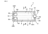
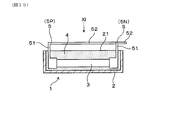
- FIG. 1 is a cross-sectional view of a resistor according to the first embodiment
- 2 is a view from II of FIG. 1
- 3 is a cross-sectional view taken along line III-III in FIG.
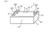
- FIG. 4 is a perspective view of a resistor according to the first embodiment
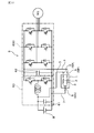
- FIG. 5 is a circuit diagram of a power conversion device mounted with a resistor according to the first embodiment
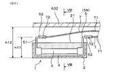
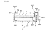
- 6 is a cross-sectional view of the mounting state of the resistor on the power conversion device in the first embodiment
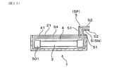
- FIG. 7 is a plan view of a resistor to which connection wiring is connected in the first embodiment
- FIG. 1 is a cross-sectional view of a resistor according to the first embodiment
- 2 is a view from II of FIG. 1
- 3 is a cross-sectional view taken along line III-III in FIG.
- FIG. 4 is a perspective view of a resistor according to the first embodiment
- FIG. 5 is a circuit diagram of a power conversion device mounted with a resistor according to
- FIG. 8 is a cross-sectional view of the mounted state of the resistor on the power conversion device, corresponding to the cross section taken along line VIII-VIII in FIG.
- FIG. 9 is a cross-sectional view of a resistor in a comparative embodiment
- FIG. 10 is a cross-sectional view of a resistor according to a second embodiment
- 11 is a view on XI in
- FIG. 12 is a cross-sectional view of a resistor according to a third embodiment
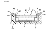
- 13 is a cross-sectional view of a resistor according to a fourth embodiment
- 14 is a cross-sectional view of a resistor according to a fifth embodiment
- 15 is a cross-sectional view of a resistor according to a sixth embodiment
- FIG. 16 is an XVI view of FIG.
- the resistor 1 of the present embodiment has a case 2, a resistor 3, a cement 4, and a lead terminal 5 as shown in FIGS. 1 to 4.
- Case 2 has an opening 21.
- the resistor 3 is accommodated in the case 2.
- the cement 4 is filled in the case 2 to embed the resistor 3 therein.
- the lead terminal 5 is connected to the resistor 3 in the cement 4 and is drawn from the cement 4 toward the opening surface 21 of the case 2.
- the lead terminal 5 has an erected portion 51 and a creeping portion 52.
- the erected portion 51 is a portion erected in the opening direction of the opening surface 21.
- the creeping portion 52 is a portion extending from the standing portion 51 in the creeping direction along the opening surface 21.
- the creeping portion 52 may be a portion extending in the creeping direction from the standing portion 51, and does not necessarily mean only a portion along the opening surface 21. That is, even if it is a portion which does not overlap the opening surface 21 when viewed from the opening direction, in the extraction terminal 5, it is a portion extending in the creeping direction along the opening surface 21 from the standing portion 51. Applicable
- the case 2 has a substantially rectangular parallelepiped shape, and one surface thereof is an opening surface 21. That is, the case 2 has a bottom surface portion 22 and four side surface portions 23 erected in the normal direction from the entire circumference of the bottom surface portion 22.
- the bottom surface portion 22 has a larger area than each side surface portion 23.
- the case 2 is formed of, for example, a ceramic.
- the resistor 3 is disposed along the bottom portion 22.
- two resistors 3 are arranged.
- Each resistor 3 has a substantially cylindrical shape.
- the resistor 3 has a shape elongated in the axial direction of a cylindrical shape.
- the two resistors 3 are arranged substantially parallel to each other. Further, the two resistors 3 are disposed at substantially the same position in the opening direction. Moreover, the both ends of each resistor 3 are mutually lined up in the sequence direction of the two resistors 3. Then, terminal members 50 made of metal are attached to both ends of the resistor 3.
- the terminal member 50 has a holding portion 501 joined to hold an end portion of the resistor 3 and a lead terminal 5 extending from the holding portion 501.
- the terminal members 50 joined to one end of the two resistors 3 are independent of each other. That is, these terminal members 50 are separate members from each other and are electrically isolated from each other.
- Each terminal member 50 has an individual lead terminal 5.
- the side on which the mutually independent terminal members 50 are provided is the positive electrode side.
- the holding parts 501 joined to the other ends of the two resistors 3 are electrically connected to each other.
- the holding portions 501 share one lead terminal 5. That is, one leadout terminal 5 is connected to the two holding portions 501.
- the side on which the holding portions 501 electrically connected to each other is provided is the negative electrode side.
- the cement 4 is filled in the case 2 so as to embed the resistor 3 therein.
- the cement 4 has an exposed surface 41 exposed to the opening surface 21 of the case 2.
- the exposed surface 41 is formed at the same position as the end surface of the side surface portion 23 of the case 2 in the opening direction.
- the exposed surface 41 is a plane substantially parallel to the opening surface 21.
- the lead terminal 5 protrudes from the exposed surface 41 in the opening direction.
- the erected portion 51 of the lead terminal 5 is substantially orthogonal to the exposed surface 41.
- the surface portion 52 of the lead terminal 5 is formed substantially parallel to the exposed surface 41.
- the creeping portion 52 is formed in a flat plate shape.
- the normal direction of the main surface of the creeping portion 52 is directed to the opening direction of the opening surface 21. That is, the surface 52 is formed substantially parallel to the opening surface 21. In other words, the creeping portion 52 is disposed to face the exposed surface 41 substantially in parallel.
- the standing portion 51 is also formed in a flat plate shape.
- the main surface of the standing portion 51 faces the longitudinal direction of the resistor 3.
- the case 2 has a shape elongated in the longitudinal direction of the resistor 3.
- the term “longitudinal direction” refers to the direction along the longitudinal direction of the resistor 3.
- the standing portion 51 and the surface portion 52 are formed in a state in which the metal plate is bent substantially at a right angle.
- the resistor 3 has a shape elongated in the direction along the opening surface 21.
- the creeping portion 52 is formed to extend in the longitudinal direction of the resistor 3 from the standing portion 51. At least one of the lead terminals 5 is disposed such that the creeping portion 52 overlaps the resistor 3 when viewed from the opening direction.
- the creeping surface portion 52 of the lead terminal 5P on the positive electrode side is disposed so as to overlap the resistor 3 in the opening direction.
- the creeping portion 52 of the lead terminal 5N on the negative electrode side does not overlap the resistor 3 as viewed from the opening direction.
- the surface portion 52 of the lead terminal 5N partially overlaps the exposed surface 41 of the cement 4 in the opening direction.
- the plurality of lead terminals 5 are formed such that the direction in which the creeping surface portion 52 extends from the erected portion 51 is the same as each other in the creeping direction.
- the resistor 1 has the three lead terminals 5, but the direction in which the creeping portion 52 extends from the standing portion 51 of the three lead terminals 5 is the same in the creeping direction. ing. That is, the three creeping portions 52 extend to the same side in the longitudinal direction. Further, the protruding height of the standing portion 51 from the opening surface 21 of the case 2 is substantially equal to all three.
- the resistor 1 is mounted on the power converter 6 whose circuit diagram is shown in FIG.
- the resistor 1 is a discharge resistor for discharging the charge of the capacitors 61 and 62.
- the power converter 6 has a booster 60 and an inverter 600 as shown in FIG. Power conversion device 6 is provided between DC power supply B and AC load MG, and performs power conversion between DC power and AC power.
- the booster 60 has a filter capacitor 61.
- the inverter unit 600 has a smoothing capacitor 62.
- the resistor 1 is configured to be able to efficiently discharge both the charge of the filter capacitor 61 and the charge of the smoothing capacitor 62. That is, one of the two resistors 3 in the resistor 1 is connected at a position electrically close to the filter capacitor 61. Further, the other resistor 3 in the resistor 1 is connected at a position electrically close to the smoothing capacitor 62. Each resistor 3 is connected in parallel with the filter capacitor 61 and the smoothing capacitor 62, respectively. Thereby, the charge of the filter capacitor 61 and the charge of the smoothing capacitor 62 can be discharged through the respective resistors 3. Therefore, it is possible to simultaneously discharge the charge of the filter capacitor 61 and the charge of the smoothing capacitor 62, which enables efficient discharge.
- connection wiring 7 has a coated conducting wire 71 and a terminal fitting 72 provided at the end thereof.
- the terminal fitting 72 of the connection wiring 7 is connected to the tip of the surface portion 52 of the lead terminal 5.
- the surface portion 52 and the terminal fitting 72 can be joined, for example, by welding, soldering or the like.
- connection wires 7 connects the positive electrode lead terminal 5P of one of the resistors 3 to a wire of the same potential as the positive electrode of the DC power supply B in the booster 60.
- the other one of the connection wires 7 connects the positive electrode lead terminal 5 P of the other resistor 3 to the positive electrode wire of the inverter unit 600.
- Yet another one of the connection wires 7 connects the negative electrode lead terminal 5N of the resistor 3 to the negative electrode wire of the booster 60 and the inverter 600.
- the resistor 1 in the state in which the connection wiring 7 is connected as described above is disposed in the housing 63 of the power conversion device 6, as shown in FIG.
- the resistor 1 is fixed to the housing 63 in a state of being mounted on the holder 64.
- the resistor 1 mounted on the holder 64 is disposed between the switching circuit unit 65 having the semiconductor module and the wall portions 631, 632 of the housing 63. That is, the resistor 1 is disposed in the gap space surrounded by the switching circuit portion 65 and the wall portions 631, 632 of the housing 63.
- the resistor 1 is disposed in a state where the opening surface 21 of the case 2 is opposed to the wall portion 632.
- the housing 63 is made of, for example, a metal member such as aluminum.
- positioning of this resistor 1 is an example, and the mounting aspect in particular is not limited.
- the resistor 1 may be mounted in the housing 63 after the connection wiring 7 is connected to the lead terminal 5, or after the resistor 1 is mounted in the housing 63, the resistor 1 may be connected to the lead terminal 5.
- the wire 7 may be connected.
- the lead-out terminal 5 has a standing portion 51 and a creeping portion 52.
- the protrusion amount of the lead-out terminal 5 in the opening direction from the case 2 can be reduced.
- downsizing of the resistor 1 in the opening direction can be achieved.
- the creeping portion 52 the direction in which the connection wiring 7 connected to the lead terminal 5 extends can be easily set to the creeping direction.
- the mounting space in the power converter 6 can be reduced in the opening direction, including the connection wiring 7.
- the mountability of the resistor 1 to the power converter 6 can be improved.
- the wall portion 632 of the housing 63 can be brought close to the opening surface 21 of the resistor 1.
- the heat dissipation of the resistor 1 can also be improved.
- the creeping portion 52 is formed in a flat plate shape, and the normal direction of the main surface thereof is directed to the opening direction. Thereby, the miniaturization of the resistor 1 in the opening direction can be further facilitated. Further, part of the noise radiated from the resistor 3 in the opening direction can be shielded by the creeping portion 52. Therefore, it is possible to suppress the influence of noise on an electronic component or the like close to the resistor 3.
- At least one of the lead terminals 5 is arranged such that the creeping portion 52 overlaps the resistor 3 when viewed from the opening direction.
- the resistor 1 can be easily miniaturized in the creeping direction. Further, part of the noise radiated from the resistor 3 in the opening direction can be shielded by the creeping portion 52. Therefore, it is possible to suppress the influence of noise on an electronic component or the like close to the resistor 3.
- the creeping portion 52 is formed to extend from the standing portion 51 in the longitudinal direction of the resistor 3.
- the size of the resistor 1 can be miniaturized not only in the opening direction but also in the width direction orthogonal to both the longitudinal direction and the opening direction. Then, as shown in FIGS. 6 and 7, even in the state where the connection wiring 7 is connected to the lead terminal 5, the connection wiring 7 can be easily arranged along the longitudinal direction. As a result, including the connection wiring 7, the mountability of the resistor 1 to the power conversion device 6 can be further improved.
- the plurality of lead terminals 5 are formed such that the direction in which the creeping surface portion 52 extends from the erected portion 51 is the same as each other in the creeping direction. Therefore, the plurality of connection wires 7 connected to the plurality of lead terminals 5 can be drawn to the same side in the creeping direction. As a result, it is easy to simplify the arrangement of the plurality of connection wires 7. For example, it is also possible to bundle a plurality of connection wires 7 partially. As a result, the mountability of the resistor 1 including the plurality of connection wires 7 can be further improved.
- the lead terminal 95 is in the form of a resistor 9 standing from the opening surface 21 in the opening direction. Others are the same as the resistor 1 of the first embodiment.
- symbols used after this comparison form represents the component similar to the thing in already-appeared embodiment, etc., unless shown otherwise.
- the lead-out terminal 95 since the lead-out terminal 95 is erected in the opening direction, the physical size in the opening direction of the resistor 9 tends to be large. That is, the dimension h91 in FIG. 9 is larger than the dimension h11 in the opening direction of the resistor 1 of the first embodiment shown in FIG. Also, the connection wiring 7 connected to the lead terminal 95 is drawn in the opening direction. Therefore, the dimension h 92 in the opening direction of the mounting space of the resistor 9 including the arrangement space of the connection wiring 7 is also larger than that in the first embodiment (dimension h 12 in FIG. 6). As described above, the resistor 9 shown in the comparative embodiment has room for improvement in terms of the mountability to the device. Compared with this, the resistor 1 of the embodiment 1 can greatly improve the mountability to the device.
- This embodiment is an embodiment of the resistor 1 in which the creeping portions 52 of a part of the lead terminals 5 are formed over the major part of the opening surface 21 in the longitudinal direction, as shown in FIGS.
- the surface portion 52 of the lead-out terminal 5 connected to one end of the resistor 3 is formed to extend to the vicinity of the other end of the resistor 3.
- the creeping surface portion 52 of the positive electrode side extraction terminal 5P is formed to be long over the major part of the opening surface 21 in the longitudinal direction. Further, the creeping portions 52 of the two lead terminals 5P are formed to be long. The long creeping surface portions 52 are disposed so as to overlap the resistor 3 when viewed from the opening direction.
- a creeping portion 52 extends outward from the other end of the resistor 3 on the negative electrode side lead-out terminal 5N.
- the creeping portions 52 of the two positive electrode side lead terminals 5P and the creeping portions 52 of the one negative electrode side lead terminal 5N extend on the same side in the longitudinal direction.
- the three creeping portions 52 are arranged in a direction perpendicular to the longitudinal direction in the creeping direction.
- the creeping surface portion 52 of the lead-out terminal 5N on the negative electrode side is disposed between the creeping portions 52 of the two positive-electrode-side lead terminals 5P.
- the other configuration is the same as that of the first embodiment.
- the creeping portion 52 of the lead terminal 5 is disposed to face the resistor 3 in the wide range from the opening direction. Therefore, the noise from the resistor 3 can be shielded more effectively by the creeping portion 52. Further, by forming the creeping surface portion 52 of a part of the lead terminals 5 to be long, it is possible to effectively dissipate the heat of the resistor 3 through the lead terminals 5. In addition, the tip end of the creeping portion 52 of the lead terminal 5 on the positive electrode side can be disposed near the tip end of the creeping portion 52 of the lead terminal 5 on the negative electrode side. Therefore, the connection wiring 7 can be efficiently connected to these lead terminals 5. In addition, it has the same operation effect as Embodiment 1.
- the creeping portions 52 of some of the lead terminals 5 have a first creeping portion 521 and a second creeping portion 522 provided at different positions in the opening direction. It is a form.
- the first creeping portion 521 extends outward from the standing portion 51 in the longitudinal direction.
- An intermediate portion 523 extends from the end of the first creeping portion 521 on the opposite side of the standing portion 51 to the bottom 22 in the opening direction.
- a second creeping portion 522 extends from the end of the intermediate portion 523 opposite to the first creeping portion 521 to the outside in the longitudinal direction of the resistor 3. Then, the connection wiring 7 is connected to the tip of the second creeping portion 522.
- the lead terminal 5 having the first creeping portion 521 and the second creeping portion 522 is the lead terminal 5N on the negative electrode side.
- the positive electrode side lead terminal 5P is the same as that of the first embodiment.
- the lead terminal 5P on the positive electrode side can also be in the same shape as the above-described lead terminal 5N on the negative electrode side.
- the other configuration is the same as that of the first embodiment.
- connection wiring 7 can be connected to the second creeping portion 522 of the lead terminal 5N. Therefore, the connection portion of the connection wiring 7 to the lead terminal 5N can be disposed closer to the bottom surface portion 22 than the opening surface 21. Therefore, it becomes easier to realize the reduction in height in the opening direction of the resistor 1 including the connection wiring 7. In addition, since the portion where the lead terminal 5N is exposed from the cement 4 is elongated, the heat dissipation of the resistor 1 through the lead terminal 5N can be further improved. In addition, it has the same operation effect as Embodiment 1.
- a part of the lead terminal 5 has an internal connection portion 54 formed along the longitudinal direction between the standing portion 51 and the holding portion 501. Is an embodiment of the invention.
- the internal connection portion 54 is embedded in the cement 4.
- the internal connection portion 54 extends from the holding portion 501 joined to one end of the resistor 3 toward the other end of the resistor 3.
- the internal connection portion 54 is disposed in the cement 4 so as to face the resistor 3 from the opening direction.
- the standing part 51 stands in the opening direction from the edge part on the opposite side to the holding part 501 in the internal connection part 54. As shown in FIG. The standing portion 51 protrudes from the opening surface 21. A creeping surface 52 is formed from the end on the opposite side to the internal connection portion 54 in the standing portion 51 toward the outside in the longitudinal direction.
- the internal connection portion 54 is provided on the lead terminal 5P on the positive electrode side.
- the lead terminal 5N on the negative electrode side is the same as that of the first embodiment. Therefore, the creeping surface portion 52 of the positive lead terminal 5P and the creeping surface 52 of the negative lead terminal 5N extend to the same side in the longitudinal direction.
- the other configuration is the same as that of the first embodiment.
- the internal connection portion 54 of the lead terminal 5 is disposed to face the resistor 3 in the wide range from the opening direction. Therefore, the noise from the resistor 3 can be shielded more effectively by the lead terminal 5.
- the internal connection portion 54 and the resistor 3 face each other in the cement 4, the distance between the two can be easily shortened. Therefore, the noise of the resistor 3 can be shielded more effectively.
- the lead terminal 5 since the surface area of the lead terminal 5 in the interior of the cement 4 can be easily increased, the lead terminal 5 can easily receive heat from the resistor 3 in the cement 4. Therefore, the heat dissipation through the lead terminal 5 can be performed more efficiently. In addition, it has the same operation effect as Embodiment 1.
- Embodiment 5 is a form of the resistor 1 configured to fix the lead terminal 5 to the bus bar 70 as shown in FIG. That is, in the present embodiment, as the connection wiring, not the wire-like coated conductive wire (see reference numeral 71 in FIG. 6 and FIG. 7) but the bus bar 70 made of a metal plate is connected to the lead terminal 5.
- the lead terminals 5 and the bus bars 70 are fastened to each other by bolts 66.
- the lead terminals 5 are fixed to the holder 64 together with the bus bars 70.
- the holder 64 is made of, for example, an insulator such as a resin.
- the surface portion 52 extends outward in the longitudinal direction of the resistor 3.
- the creeping portion 52 is extended to the outside of the outer shape of the case 2 sufficiently.
- the creeping portion 52 of the lead terminal 5 is stacked with the bus bar 70 in the opening direction. Insertion holes through which the bolts 66 are respectively inserted are formed in the bus bar 70 and the surface portion 52. The bolt 66 is inserted into these insertion holes and screwed to the female screw provided in the holder 64, thereby fastening the lead terminal 5 together with the bus bar 70 to the holder 64.
- the other configuration is the same as that of the first embodiment.
- the lead terminal 5 can be directly fixed to the bus bar 70. Therefore, the vibration of the lead terminal 5 can be suppressed. As a result, the vibration resistance of the connection portion can be improved. Further, the heat of the resistor 1 can be easily dissipated to the bus bar 70. Therefore, it is possible to obtain the resistor 1 further excellent in heat dissipation. In addition, it has the same operation effect as Embodiment 1.
- Embodiment 6 This embodiment is an embodiment of the resistor 1 in which two resistors 3 are arranged in the longitudinal direction as shown in FIGS.
- the negative electrode side lead terminals 5N connected to each other are disposed at the central portion in the longitudinal direction.
- the lead terminals 5N on the negative electrode side of the two resistors 3 are connected to each other.
- At least one of the lead terminals 5N on the negative electrode side of the two resistors 3 has a creeping portion 52.
- the two positive electrode side lead terminals 5P are disposed near both ends in the longitudinal direction. And the creepage part 52 of these lead-out terminals 5P is prolonged to the outside in the longitudinal direction.
- the other configuration is the same as that of the first embodiment.
- miniaturization of the resistor 1 can be achieved in the direction orthogonal to both the longitudinal direction and the opening direction.
- it is suitable when arranging the resistor 1 in an elongated space in the power conversion device.
- it has the same operation effect as Embodiment 1.
- the number of resistors of the resistor can be one or three or more.
Landscapes
- Engineering & Computer Science (AREA)
- Microelectronics & Electronic Packaging (AREA)
- Details Of Resistors (AREA)
Abstract
L'invention concerne une résistance (1) comprenant : un boîtier (2) comprenant un plan d'ouverture (21) ; un élément résistif (3) contenu dans le boîtier (2) ; un ciment (4) avec lequel le boîtier (2) est rempli pour incorporer l'élément résistif (3) ; et des bornes de sortie (5) qui sont reliées à l'élément résistif (3) dans le ciment (4) et sortent du ciment (4) sur le côté du plan d'ouverture (21) du boîtier (2). Les bornes de sortie (5) comprennent une partie montante (51) s'élevant dans la direction de l'ouverture du plan d'ouverture (21), et une partie de surface (52) s'étendant à partir de la partie montante (51) dans une direction de surface le long du plan d'ouverture (21).
Priority Applications (2)
| Application Number | Priority Date | Filing Date | Title |
|---|---|---|---|
| CN201880060480.7A CN111133536B (zh) | 2017-09-20 | 2018-09-14 | 电阻器 |
| US16/825,917 US10964458B2 (en) | 2017-09-20 | 2020-03-20 | Resistor unit |
Applications Claiming Priority (2)
| Application Number | Priority Date | Filing Date | Title |
|---|---|---|---|
| JP2017-179915 | 2017-09-20 | ||
| JP2017179915A JP6855991B2 (ja) | 2017-09-20 | 2017-09-20 | 抵抗器 |
Related Child Applications (1)
| Application Number | Title | Priority Date | Filing Date |
|---|---|---|---|
| US16/825,917 Continuation US10964458B2 (en) | 2017-09-20 | 2020-03-20 | Resistor unit |
Publications (1)
| Publication Number | Publication Date |
|---|---|
| WO2019059129A1 true WO2019059129A1 (fr) | 2019-03-28 |
Family
ID=65810761
Family Applications (1)
| Application Number | Title | Priority Date | Filing Date |
|---|---|---|---|
| PCT/JP2018/034217 Ceased WO2019059129A1 (fr) | 2017-09-20 | 2018-09-14 | Résistance |
Country Status (4)
| Country | Link |
|---|---|
| US (1) | US10964458B2 (fr) |
| JP (1) | JP6855991B2 (fr) |
| CN (1) | CN111133536B (fr) |
| WO (1) | WO2019059129A1 (fr) |
Families Citing this family (1)
| Publication number | Priority date | Publication date | Assignee | Title |
|---|---|---|---|---|
| CN121127933A (zh) * | 2023-08-31 | 2025-12-12 | 株式会社Lg新能源 | 电阻单元、电阻组件和电池组 |
Citations (5)
| Publication number | Priority date | Publication date | Assignee | Title |
|---|---|---|---|---|
| JPH0176001U (fr) * | 1987-11-10 | 1989-05-23 | ||
| JPH031402U (fr) * | 1989-05-22 | 1991-01-09 | ||
| JPH03128902U (fr) * | 1990-04-09 | 1991-12-25 | ||
| JP2009038275A (ja) * | 2007-08-03 | 2009-02-19 | Koa Corp | セメント抵抗器 |
| JP2014036145A (ja) * | 2012-08-09 | 2014-02-24 | Toyota Industries Corp | 抵抗装置 |
Family Cites Families (11)
| Publication number | Priority date | Publication date | Assignee | Title |
|---|---|---|---|---|
| US2538977A (en) * | 1949-11-23 | 1951-01-23 | Clarostat Mfg Co Inc | Resistor |
| US3581266A (en) * | 1968-12-30 | 1971-05-25 | Lionel E Weyenberg | Housed resistor |
| US3728660A (en) * | 1969-11-21 | 1973-04-17 | Thermo Couple Prod Co Inc | Temperature responsive resistance element for a temperature sensitive control sensor |
| US3668598A (en) * | 1970-10-23 | 1972-06-06 | Emerson Electric Co | Electric heating elements |
| US5888102A (en) * | 1996-11-25 | 1999-03-30 | Strickland; John | Surface mount carrier for electronic components |
| JP4846434B2 (ja) * | 2006-05-09 | 2011-12-28 | コーア株式会社 | セメント抵抗器 |
| US9530545B2 (en) * | 2013-06-28 | 2016-12-27 | Zhonghou Xu | Device comprising a thermal fuse and a resistor |
| JP2016019384A (ja) | 2014-07-09 | 2016-02-01 | 株式会社豊田自動織機 | 電子機器 |
| JP6420590B2 (ja) | 2014-08-18 | 2018-11-07 | ミクロン電気株式会社 | セメント抵抗器 |
| JP6694303B2 (ja) * | 2016-03-24 | 2020-05-13 | Koa株式会社 | 面実装型抵抗器 |
| US20180047539A1 (en) * | 2016-08-10 | 2018-02-15 | Smart Electronics Inc. | Fuse resistor and method of manufacturing the same |
-
2017
- 2017-09-20 JP JP2017179915A patent/JP6855991B2/ja active Active
-
2018
- 2018-09-14 WO PCT/JP2018/034217 patent/WO2019059129A1/fr not_active Ceased
- 2018-09-14 CN CN201880060480.7A patent/CN111133536B/zh active Active
-
2020
- 2020-03-20 US US16/825,917 patent/US10964458B2/en active Active
Patent Citations (5)
| Publication number | Priority date | Publication date | Assignee | Title |
|---|---|---|---|---|
| JPH0176001U (fr) * | 1987-11-10 | 1989-05-23 | ||
| JPH031402U (fr) * | 1989-05-22 | 1991-01-09 | ||
| JPH03128902U (fr) * | 1990-04-09 | 1991-12-25 | ||
| JP2009038275A (ja) * | 2007-08-03 | 2009-02-19 | Koa Corp | セメント抵抗器 |
| JP2014036145A (ja) * | 2012-08-09 | 2014-02-24 | Toyota Industries Corp | 抵抗装置 |
Also Published As
| Publication number | Publication date |
|---|---|
| JP6855991B2 (ja) | 2021-04-07 |
| CN111133536A (zh) | 2020-05-08 |
| CN111133536B (zh) | 2022-10-04 |
| US10964458B2 (en) | 2021-03-30 |
| JP2019057558A (ja) | 2019-04-11 |
| US20200219639A1 (en) | 2020-07-09 |
Similar Documents
| Publication | Publication Date | Title |
|---|---|---|
| JP7065595B2 (ja) | フィルムコンデンサモジュール | |
| JP5897918B2 (ja) | コンデンサ | |
| JP6152722B2 (ja) | ノイズフィルタ装置 | |
| CN108370197B (zh) | 电路板、非驱动端罩、电动机套件和电动机 | |
| JP5645544B2 (ja) | コンデンサ | |
| JP5989321B2 (ja) | コンデンサ | |
| JP2009027778A (ja) | バスバー | |
| CN106061143A (zh) | 电子控制单元 | |
| WO2019107128A1 (fr) | Condensateur | |
| WO2019059129A1 (fr) | Résistance | |
| EP3611835B1 (fr) | Dispositif de conversion d'énergie électrique | |
| JP5672216B2 (ja) | 接続コネクタ | |
| WO2020153164A1 (fr) | Structure de circuit, boîte de connexion électrique, et procédé de fabrication de structure de circuit | |
| JP7040334B2 (ja) | 電力変換装置 | |
| JP7031452B2 (ja) | コンデンサ | |
| JP2017050335A (ja) | スナバモジュール | |
| WO2020203615A1 (fr) | Dispositif de conversion de puissance | |
| JP6146739B2 (ja) | 直流高電圧電源装置 | |
| JP7134305B1 (ja) | 電力変換装置 | |
| JP7148376B2 (ja) | リアクトル | |
| JP6218876B2 (ja) | モジュール部品およびその製造方法 | |
| JP2004119874A (ja) | コンデンサ及びその製造方法 | |
| JP4609036B2 (ja) | 回路モジュール | |
| JP2015091076A (ja) | 電子部品モジュールおよびその搭載方法 | |
| CN113823945A (zh) | 电子装置 |
Legal Events
| Date | Code | Title | Description |
|---|---|---|---|
| 121 | Ep: the epo has been informed by wipo that ep was designated in this application |
Ref document number: 18859676 Country of ref document: EP Kind code of ref document: A1 |
|
| NENP | Non-entry into the national phase |
Ref country code: DE |
|
| 122 | Ep: pct application non-entry in european phase |
Ref document number: 18859676 Country of ref document: EP Kind code of ref document: A1 |