WO2019059342A1 - Dispositif guide d'ondes optiques, dispositif de conversion photoélectrique, bâtiment, dispositif électronique, corps mobile et dispositif guide d'ondes électromagnétiques - Google Patents
Dispositif guide d'ondes optiques, dispositif de conversion photoélectrique, bâtiment, dispositif électronique, corps mobile et dispositif guide d'ondes électromagnétiques Download PDFInfo
- Publication number
- WO2019059342A1 WO2019059342A1 PCT/JP2018/035015 JP2018035015W WO2019059342A1 WO 2019059342 A1 WO2019059342 A1 WO 2019059342A1 JP 2018035015 W JP2018035015 W JP 2018035015W WO 2019059342 A1 WO2019059342 A1 WO 2019059342A1
- Authority
- WO
- WIPO (PCT)
- Prior art keywords
- core layer
- light
- waveguide
- layer
- optical waveguide
- Prior art date
- Legal status (The legal status is an assumption and is not a legal conclusion. Google has not performed a legal analysis and makes no representation as to the accuracy of the status listed.)
- Ceased
Links
Images


Classifications
-
- G—PHYSICS
- G02—OPTICS
- G02B—OPTICAL ELEMENTS, SYSTEMS OR APPARATUS
- G02B6/00—Light guides; Structural details of arrangements comprising light guides and other optical elements, e.g. couplings
- G02B6/10—Light guides; Structural details of arrangements comprising light guides and other optical elements, e.g. couplings of the optical waveguide type
- G02B6/12—Light guides; Structural details of arrangements comprising light guides and other optical elements, e.g. couplings of the optical waveguide type of the integrated circuit kind
- G02B6/122—Basic optical elements, e.g. light-guiding paths
-
- G—PHYSICS
- G02—OPTICS
- G02B—OPTICAL ELEMENTS, SYSTEMS OR APPARATUS
- G02B6/00—Light guides; Structural details of arrangements comprising light guides and other optical elements, e.g. couplings
- G02B6/24—Coupling light guides
- G02B6/26—Optical coupling means
- G02B6/28—Optical coupling means having data bus means, i.e. plural waveguides interconnected and providing an inherently bidirectional system by mixing and splitting signals
-
- H—ELECTRICITY
- H10—SEMICONDUCTOR DEVICES; ELECTRIC SOLID-STATE DEVICES NOT OTHERWISE PROVIDED FOR
- H10F—INORGANIC SEMICONDUCTOR DEVICES SENSITIVE TO INFRARED RADIATION, LIGHT, ELECTROMAGNETIC RADIATION OF SHORTER WAVELENGTH OR CORPUSCULAR RADIATION
- H10F77/00—Constructional details of devices covered by this subclass
- H10F77/40—Optical elements or arrangements
- H10F77/42—Optical elements or arrangements directly associated or integrated with photovoltaic cells, e.g. light-reflecting means or light-concentrating means
-
- Y—GENERAL TAGGING OF NEW TECHNOLOGICAL DEVELOPMENTS; GENERAL TAGGING OF CROSS-SECTIONAL TECHNOLOGIES SPANNING OVER SEVERAL SECTIONS OF THE IPC; TECHNICAL SUBJECTS COVERED BY FORMER USPC CROSS-REFERENCE ART COLLECTIONS [XRACs] AND DIGESTS
- Y02—TECHNOLOGIES OR APPLICATIONS FOR MITIGATION OR ADAPTATION AGAINST CLIMATE CHANGE
- Y02B—CLIMATE CHANGE MITIGATION TECHNOLOGIES RELATED TO BUILDINGS, e.g. HOUSING, HOUSE APPLIANCES OR RELATED END-USER APPLICATIONS
- Y02B10/00—Integration of renewable energy sources in buildings
- Y02B10/10—Photovoltaic [PV]
-
- Y—GENERAL TAGGING OF NEW TECHNOLOGICAL DEVELOPMENTS; GENERAL TAGGING OF CROSS-SECTIONAL TECHNOLOGIES SPANNING OVER SEVERAL SECTIONS OF THE IPC; TECHNICAL SUBJECTS COVERED BY FORMER USPC CROSS-REFERENCE ART COLLECTIONS [XRACs] AND DIGESTS
- Y02—TECHNOLOGIES OR APPLICATIONS FOR MITIGATION OR ADAPTATION AGAINST CLIMATE CHANGE
- Y02E—REDUCTION OF GREENHOUSE GAS [GHG] EMISSIONS, RELATED TO ENERGY GENERATION, TRANSMISSION OR DISTRIBUTION
- Y02E10/00—Energy generation through renewable energy sources
- Y02E10/50—Photovoltaic [PV] energy
- Y02E10/52—PV systems with concentrators
Definitions
- the present invention relates to an optical waveguide device, a photoelectric conversion device, a building, an electronic device, a movable body, and an electromagnetic wave waveguide device. More specifically, the present invention is applied to efficiently collect light such as ultraviolet light, visible light, infrared light and the like, and to guide the light at high efficiency without loss along the way.
- electromagnetic waves such as photoelectric conversion devices, buildings using the photoelectric conversion devices, electronic devices and moving bodies, and microwaves, and to efficiently guide the electromagnetic waves without loss along the way
- the present invention relates to an electromagnetic wave waveguide device suitable for application.
- a waveguide is a circuit or line that confines and transmits waves in a certain area and is defined as a system or material designed to confine and direct electromagnetic waves in a direction determined by physical boundaries. Be done.
- an optical fiber or a two-dimensional waveguide (slab type optical waveguide) is well known as a structure for guiding an electromagnetic wave, particularly light, long distance without causing loss in the middle.
- waveguides have continuous translational symmetry in order to confine light for transmission.
- small refractive index parts that is, the clad layer and large refractive index parts, that is, the core layer, which have unevenness in the upper surface and thickness variation of one-sided flow, but their cross section is a simple closed surface .
- the area of the cross section is S and the outer peripheral length defining the area is L
- the area S of the cross section is surrounded efficiently, that is, by a relatively short L. It is given by S to cL 2 but 1 / c is an amount of the order of 10, such as 12 to 50 (12 corresponds to a circle, 50 corresponds to a flat bowl-like structure) (see, for example, Patent Document 1). ).
- an optical multiplexing / demultiplexing device which combines a plurality of light and splits the light by using a flat substrate, but this is in an optical integrated circuit, and the optical multiplexing (focusing)
- the branching operation is performed only a few times at approximately 34 mm, extremely sparsely, over several mm in order to reduce the loss (see Non-Patent Document 1).
- the net distance at which this light collection process occurs is basically a short distance (which will increase the degree of integration in the future), and it is possible to densely combine light
- the presence area of light is also linear.
- Non-Patent Document 2 Luminescent Solar Concentrator (LSC) (see Non-Patent Document 2) has attracted attention in order to increase the efficiency of photovoltaic power generation, and in particular, to configure the system as a light collection system. .
- LSC Luminescent Solar Concentrator
- the above two-dimensional waveguide is included as an important component.
- all the prior art implicitly assumes symmetrical waveguides with continuous translational symmetry.
- the conventional waveguide has a symmetrical structure with respect to the light guiding direction with respect to the forward direction and the reverse direction, and basically, a structure in which a core layer for guiding light is continuously sandwiched and surrounded by a cladding layer, The light was prevented from leaking and confined. For this reason, it was extremely difficult to introduce light into the waveguide core layer from the outside. Since we do not want to lower the light guiding efficiency, it can be said that it was not supposed in the first place. Under such circumstances, when the conventional waveguide is combined with a concentrating solar cell or a photoelectric conversion element, there are great difficulties in efficiently condensing light. That is, the light incident on the luminescent solar concentrator does not have total reflection because there is also a component to return.
- Luminescent solar concentrators use dyes and quantum dots, but dyes and quantum dots can not totally absorb sunlight (there is a component to escape). In addition, there is light reabsorption by the dye, and the life of the dye is not long. Furthermore, it is difficult to confine light in a luminescent solar concentrator, and light emission is basically isotropic, so that light that does not satisfy the total reflection condition may exit into space (Non-Patent Document 3). reference.). As a result, the photoelectric conversion efficiency in the solar cell can not be increased.
- the light introduction portion is basically limited to the end point (only the start point of the fiber or waveguide) in order to guide the light over a long distance without causing loss.
- the optical fiber or two-dimensional waveguide is basically from the starting point of the fiber (the light incident surface of the two-dimensional waveguide) to the end point of the fiber Up to (the light exit surface of the two-dimensional waveguide), there was continuous translational symmetry along the traveling direction of light.
- the waveguide structure in a structure for delivering such light to a distance, even if light in / out is reversed because there is translational symmetry with respect to the structure between the start point and the end point, that is, the end point It is characteristic that even when light is introduced, the light can reach the starting point with the same high waveguide efficiency. That is, for the sake of simplicity, when the waveguide structure is arranged in a straight line connecting the start point on the left and the end point on the right, this structure has left and right space inversion symmetry.
- the waveguide may be said to have inversion symmetry with respect to the light guiding direction with respect to the forward direction and the reverse direction.
- the problem to be solved by the present invention is to keep the waveguide efficiency of the waveguide core layer high while using the light introducing core layer from the position in the middle of the waveguide core layer to emit light such as sunlight from the outside
- An optical waveguide device capable of efficiently condensing external light and guiding the light efficiently inside the waveguide core layer; and a light emitting portion of the optical waveguide device. It is an object of the present invention to provide a photoelectric conversion device capable of obtaining extremely high photoelectric conversion efficiency by causing the incident light to enter the photoelectric conversion portion, and a building, an electronic device, and a movable body using the photoelectric conversion device.
- Another problem to be solved by the present invention is that while the waveguide efficiency of the waveguide core layer is kept high, the electromagnetic wave from the outside such as microwaves by the electromagnetic wave introducing core layer from the position in the middle of the waveguide core layer It is an object of the present invention to provide an electromagnetic wave guiding device or an antenna device which can introduce an external electromagnetic wave efficiently and can efficiently guide the electromagnetic wave inside the waveguiding core layer.
- the present invention is A waveguide core layer, And a cladding layer covering the waveguide core layer discontinuously,
- the cladding layer is apart from the end of the disconnection portion not covering the waveguide core layer and the waveguide core layer opposite to the waveguide direction of the waveguide core layer with respect to the disconnection portion.
- Extending between and gradually approaching the guiding core layer towards the guiding direction of the guiding core layer, and a tangent at the end of the break parallel or substantially parallel to the guiding core layer It has a structure provided parallel to its part,
- the light introducing core layer coated with the cladding layer is provided at the disconnection portion of the cladding layer so as to merge with the waveguide core layer.
- This optical waveguide device is configured as described above, and thus has an asymmetric structure with respect to the waveguide direction of the waveguide core layer and the opposite direction.
- the waveguide core layer has continuous translational symmetry with respect to the waveguide direction
- the cladding layer has discrete translational symmetry with respect to the waveguide direction.
- the guiding direction can be reworded as the moving direction of light energy.
- the wavelength of light targeted by the optical waveguide device is not particularly limited, and includes ultraviolet light, visible light, infrared light, and the like.
- a plurality of disconnection portions of the cladding layer are provided at equal intervals in the waveguide direction of the waveguide core layer, and the light introducing core layer is provided on each of the disconnection portions.
- the spacing of the disconnections is chosen as required.
- the light introducing core layer and the cladding layer covering the light introducing core layer are waveguide cores in which light introduced to the light introducing core layer repeats total reflection at the interface between the light introducing core layer and the cladding layer. It is provided to reach the layer. More specifically, the shape and thickness (thickness) of the light introducing core layer and the cladding layer are such that as much as possible of the light introduced into the light introducing core layer reaches the waveguide core layer. Optimized.
- the cladding layer extending from the end of the discontinuity has a concavely curved shape in the waveguide direction of the waveguide core layer (more precisely, it is concavely curved in the waveguide direction of the waveguide core layer) Part of the shape).
- This shape is, for example, a shape of a circular arc of a quarter circle, or a shape of a partial arc of a quarter divided by the major and minor axes of an ellipse, but is not limited thereto.
- the cladding layer extending from the end of the disconnection portion may have a straight portion on the light incident side and a curved portion connected to the straight portion.
- the refractive index, material, size (thickness of each layer, thickness, length, etc.) of the waveguide core layer, cladding layer and light introducing core layer are appropriately selected according to the purpose of use of the optical waveguide device.
- the refractive index of the waveguide core layer and the light introducing core layer is selected to be 1.6 or more and 2.0 or less, and the material is resin or glass.
- the refractive index of the cladding layer is 1.8 or more and 2.0 or less, and is selected to be lower than the refractive indexes of the waveguide core layer and the light introducing core layer.
- the material of the waveguide core layer and the light introducing core layer is, for example, transparent glass, high refractive index glass, transparent plastic or the like.
- transparent plastics examples include polyethylene terephthalate, polyethylene naphthalate, polycarbonate, polystyrene, polyethylene, polypropylene, polyphenylene sulfide, polyvinylidene fluoride, acetyl cellulose, brominated phenoxy, aramids, polyimides, polystyrenes, polyarylates, Polysulfones, polyolefins and the like can be mentioned.
- a fluorine-based material used for plastic optical fiber (POF) or the like is preferable because of its low light loss property.
- the material of the cladding layer examples include, but not limited to, amorphous fluorine resin (trade name CYTOP of Asahi Glass Co., Ltd.) (refractive index: 1.34).
- the optical waveguide device has a waveguide core layer and a cladding layer at least over a distance of 1000 times to 100,000 times the wavelength of light guided to the waveguide core layer.
- the overall size of the optical waveguide device is appropriately selected according to the purpose of use of the optical waveguide device, etc., but generally it is, for example, (1 cm to 1 m) ⁇ (1 cm to 1 m).
- the optical waveguide device can be configured flexibly by selecting the material, thickness, etc., as needed.
- the shape of the waveguide core layer is selected according to need, and for example, it may be formed into a flat shape, a fibrous shape, or the like.
- the waveguide core layer is formed in a flat plate shape, and the cladding layer covers the one main surface of the waveguide core layer continuously to provide translational symmetry in the waveguide direction of the waveguide core layer.
- the cladding layer covers the one main surface of the waveguide core layer continuously to provide translational symmetry in the waveguide direction of the waveguide core layer.
- the waveguide core layer is formed in a flat plate shape, and the cladding layer is provided to discontinuously cover one main surface and the other main surface of the waveguide core layer,
- the main surface and the other main surface each have a disconnection portion, and the disconnection portion is provided with a light introducing core layer.
- the disconnecting portion of one main surface of the waveguide core layer and the disconnecting portion of the other main surface are mutually offset in the waveguide direction of the waveguide core layer, and most preferably, the disconnecting portion Are offset from each other by a distance of 1/2 of the interval of.
- the waveguide core layer is configured in a fiber shape
- the cladding layer is provided so as to cover the outer peripheral surface of the waveguide core layer discontinuously, and has a break in the outer peripheral surface, Is provided with a light introducing core layer.
- this optical waveguide device the basic concept of the above-mentioned conventional waveguide structure is changed, and a left-right (or forward-reverse direction) asymmetric waveguide structure having discrete translational symmetry is adopted. That is, with respect to the light guiding direction, a waveguide having no inversion symmetry is configured in the forward direction and the reverse direction. That is, the waveguide has an asymmetric structure with respect to the light guiding direction with respect to the forward direction and the reverse direction. Alternatively, it may be rephrased to have an asymmetric structure in the light traveling direction.
- the cladding layer has discontinuity and the waveguide core layer has semi-release.
- the main waveguide portion in the structure i.e., the waveguide core layer having a relatively large refractive index, has a reverse cleavage structure (i.e., a structure in which two parts are integrated into one).
- the waveguide core layer becomes a quasi-open system core layer and confines light, but has an open structure in terms of geometrical structure.
- each non-continuous cladding layer has a geometric structure that is tangential to the waveguide core layer along the waveguide direction with respect to the waveguide direction and at its last end. Have a structure that is in contact with
- the two separate large refractive index parts merge into one, but from one of the two large refractive index parts, in the above-mentioned cladding layer termination zone, according to the principle of Huygens
- the cladding layer has a gentle curve satisfying the total reflection condition by the cladding layer. Draw. This is also a condition that the remaining one large refractive index layer, ie, the light introducing core layer and its adjacent cladding layer fill the other of the two refractive index large layers.
- the light in the two large refractive index layers (waveguide core layer and light introducing core layer) which are joined spreads to the other side according to the principle of Huygens after the end of the intermediate cladding layer to the other side.
- the light is totally reflected by the cladding layer adjacent to the large refractive index layer to which it is diffused. This realizes a situation in which no loss due to the merging of light occurs.
- the light in the waveguide core layer is guided 100% along the waveguide direction, but due to the discontinuity of the cladding layer and the quasi-release property of the waveguide core layer, the light is guided in the waveguide core layer. It enables light introduction from the outside world at multiple points in the wave direction.
- the reflection optical system is constituted by the light introducing core layer and the cladding layer covering the light introducing core layer, and the wavelength dependence is extremely small, and the light condensing and the highly efficient waveguide It is extremely effective for the purpose.
- this optical waveguide device is applied to a conventional building material such as a window or wall of a building, for example, by coupling it to a waveguide having a surface structure so that incident light is guided in a glass surface. Also, it can help to solve and alleviate the problem of the right to the sun.
- this invention is An optical waveguide device, And a photoelectric conversion unit provided in the light emitting unit of the optical waveguide device,
- the above optical waveguide device is A waveguide core layer, And a cladding layer covering the waveguide core layer discontinuously, The cladding layer is apart from the end of the disconnection portion not covering the waveguide core layer and the waveguide core layer opposite to the waveguide direction of the waveguide core layer with respect to the disconnection portion.
- the optical waveguide device is provided such that a light introducing core layer covered with the cladding layer is joined to the waveguide core layer at the disconnection portion of the cladding layer,
- the photoelectric conversion device according to the present invention is a photoelectric conversion device in which light incident on a light incident portion of the optical waveguide device is emitted from a light emitting portion of the optical waveguide device and is incident on the photoelectric conversion portion.
- the photoelectric conversion portion may be provided in direct contact with the light emitting portion of the optical waveguide device, or may be provided to the light emitting portion of the optical waveguide device via a conventionally known optical waveguide. Good.
- the light when light is incident on the photoelectric conversion device, the light is not directly incident on the photoelectric conversion unit.
- the semiconductor layer can be prevented from being heated by the light directly incident on the photoelectric conversion portion, particularly the semiconductor layer, and the temperature rise can be prevented, so that the characteristic deterioration of the semiconductor layer can be prevented.
- the energy dissipated as heat is also small, a reduction in the photoelectric conversion efficiency of this photoelectric conversion device can be prevented, and high photoelectric conversion efficiency can be obtained.
- the photoelectric conversion portion may be configured by a semiconductor layer, or may be configured by a photoelectric conversion element using a semiconductor layer such as a solar cell.
- a photoelectric conversion element a conventionally known one can be used, and it is selected as necessary.
- it is a photoelectric conversion element using bulk silicon, polycrystalline silicon, CIS, a perovskite substance, a compound semiconductor or the like. Since this photoelectric conversion device forms a light collecting system, coupling with a tandem solar cell is effective.
- the light collection ratio is a value obtained by dividing the sum of the area of the end face of the light introducing core layer on the light incident surface of the optical waveguide device by the area of the end face of the waveguide core layer where light is guided.
- tandem solar cells to be coupled are also effective in parallel type. In this case, light is incident parallel or almost parallel to the pn junction plane, but first enters the widest gap element, and the band gap decreases sequentially and finally enters the solar cell with the smallest band gap. Things are common.
- bonded the optical waveguide apparatus of this invention, and a photoelectric conversion element, ie, a solar cell, in a practical use example is that a sunlight receiving part and a photoelectric conversion part are mutually isolate
- the photoelectric conversion unit can be protected by guiding light as energy from the light collecting unit placed on the roof or the side of the building as light energy to the room, the attic, the side wall back, etc. and performing photoelectric conversion there. It is a great advantage to be able to alleviate the requirements for weather resistance of solar cells.
- the present invention can also be configured to straddle in the form of light It is. That is, in the prior art, since the light receiving portion and the photoelectric conversion portion are integrated, they are present outdoors or outside the vehicle in the form of electricity which is weak to rain, frost, snow and snow. Because it exists in the form of neutral light in the open air or outside of the vehicle, it can be set so that malfunction or failure due to poor insulation such as electrical shorting does not occur. In turn, weatherability can be enhanced.
- the photoelectric conversion unit In the case of application to a house or a building, in particular, the light collecting unit is outdoors, the photoelectric conversion unit is indoors or inside the building outer wall, and protects the active region (photoelectric conversion unit) from damage by rain and dew. In particular, protection of the power generation system from salt damage on remote islands and the like is facilitated.
- the light collecting part can protect the active region (photoelectric converting part) from radiation damage in the space, and the photoelectric conversion part in the ship or inside the outer wall of the spacecraft.
- the semiconductor layer is made of an inorganic semiconductor or an organic semiconductor, and is typically a pn junction composed of a p-type semiconductor layer and an n-type semiconductor layer.
- the semiconductor layer is also formed into a flat plate, and the pn junction surface is parallel or perpendicular to the main surface of the waveguide core.
- the first electrode and the second electrode are provided on the upper and lower opposite main surfaces of the semiconductor layer.
- the semiconductor layer is formed in a flat plate or fiber shape having an end face having a size equal to or greater than the end face of the waveguide core layer, and its pn junction face is It is parallel or perpendicular to the longitudinal cross section including the diameter of the waveguide core layer.
- the first electrode and the second electrode are provided on the upper and lower surfaces of the semiconductor layer facing each other. One of these first and second electrodes is used as an anode electrode, and the other is used as a cathode electrode.
- the net traveling direction of light guided inside the waveguide core layer and the net migration of carriers generated in the semiconductor layer by the light incident on the semiconductor layer from the end face of the waveguide core layer is approximately perpendicular.
- ⁇ is selected, for example, as ⁇ / 2 ⁇ ⁇ ⁇ ⁇ ⁇ / 2 + ⁇ .
- ⁇ is used as an anode electrode of the first electrode and the second electrode, the ratio of the thickness of the semiconductor layer to the width (electrode width) in the direction parallel to the traveling direction of light in the semiconductor layer And the thickness of the semiconductor layer / the electrode width.
- the waveguide core layer and the semiconductor layer are provided integrally with each other, for example, their ends are joined and integrated.
- the thickness of the semiconductor layer is appropriately selected in consideration of the function of the diffusion length of carriers in the semiconductor layer, but preferably 100 nm when the pn junction surface is parallel to the main surface of the flat waveguide core layer. In the case where the pn junction surface is perpendicular to the main surface of the flat waveguide core layer, the thickness is preferably 1 ⁇ m to 500 ⁇ m.
- the semiconductor constituting the semiconductor layer may be in any form of amorphous (amorphous), polycrystal and single crystal.
- II-VI group compound semiconductors such as CdSe, PbS, PbSe and PbTe
- III-V group compound semiconductors such as GaSb, InAs, InN, AlInN, GaInN, GaN, AlGaN, GaAsN, GaPN, Si and SiGe Group IV semiconductors such as Si x Ge y Sn 1-xy O, SiN x , SiO x , CIS (CuInSe), CIGS (CuInGaSe), CuInGaSeTe, and the like
- These semiconductors are characterized in that their band gap can be controlled by, for example, controlling the composition ratio of Group III elements such as In and Ga, mixing sulfur (S), and the like.
- the semiconductor layer can also be composed of fine particles of these inorganic semiconductors.
- any of those generally reported as materials for organic solar cells can be used.
- polyacene such as pentacene, polyacetylene (preferably disubstituted polyacetylene), poly (p (p) -Phenylenevinylene), poly (2,5-thienylenevinylene), polypyrrole, poly (3-methylthiophene), polyaniline, poly (9,9-dialkylfluorene) (PDAF), poly (9,9-dioctylfluorene) co-bithiophene) (F8T2), poly (1-hexyl-2-phenylacetylene) (PH X PA) (shows blue emission as light emitting material), poly (diphenylacetylene) derivative (PDPA-nBu) (light emitting material As green light), poly (pyridine) (PPy), poly (pyridylbi) It is possible to use, for example, len (PPyV), cyano-substituted poly
- alkali metals Li, Na, K, Cs
- halogens Br 2 , I 2 , CI 2
- Lewis acids BF 3 , PF 5 , AsF 5 , SbF 5 , SO 3
- transition metal halides FeCl 3 , MoCl 5 , WCl 5 , SnCl 4
- TCNE and TCNQ can be used as the organic acceptor molecule.
- dopant ions used in the tetraethylammonium ions as cations (TEA +), tetrabutylammonium Ion (TBA +), Li +, Na +, K +, ClO 4 as the anion -, BF 4 -, PF 6 -, AsF 6 -, SbF 6 -.
- polyelectrolytes can also be used, and specific examples of the polyelectrolyte include, as polyanions, sulfonate polyaniline, poly (thiophene-3-acetic acid), sulfonate polystyrene, poly (3-thiophene) (Eg, alkanesulfonates), polycations such as polyallylamine, poly (p-phenylene-vinylene) precursor polymer, poly (p-methylpyridinium vinylene), protonated poly (p-pyridylvinylene), poloton N-methyl pyridinium acetylene) and the like can be used.
- polyanions such as polyanions, sulfonate polyaniline, poly (thiophene-3-acetic acid), sulfonate polystyrene, poly (3-thiophene) (Eg, alkanesulfonates), polycations such as polyallylamine, poly (p-phenylene-vinylene)
- the organic semiconductor layer can have a hetero junction type or a bulk hetero junction type structure.
- the p-type organic semiconductor film and the n-type organic semiconductor film are bonded to be in contact with the first electrode and the second electrode.
- the organic semiconductor layer having a bulk heterojunction structure is made of a mixture of p-type organic semiconductor molecules and n-type organic semiconductor molecules, and has a fine structure in which the p-type organic semiconductor and the n-type organic semiconductor are intricately in contact with each other.
- an organic-inorganic hybrid semiconductor in addition to the inorganic semiconductor and the organic semiconductor, an organic-inorganic hybrid semiconductor can also be used.
- an organic-inorganic hybrid semiconductor for example, a perovskite semiconductor can be used.
- the first electrode and the second electrode are in ohmic contact with the semiconductor layer.
- the first electrode and the second electrode may not be in ohmic contact with the semiconductor layer.
- metals such as gold (Au), nickel (Ni) and aluminum (Al) for the first electrode and the second electrode
- Al may be used particularly for p-type Si and Ag for n-type Si. It is effective, and various transparent conductive oxides such as indium-tin oxide (ITO), zinc oxide (ZnO), tin oxide (SnO), etc. can be used, and chromium, titanium, molybdenum etc. are also used together although it is possible, it is not limited to this.
- the transparent electrode in the case of using a transparent electrode made of the above-mentioned transparent conductive oxide as the first electrode and the second electrode, high waveguide characteristics of incident photons to the semiconductor layer can be obtained with low refractive index and wide gap properties. This also has the effect of leading to a low surface recombination rate of the generated photocarrier and consequently enabling high photoelectric conversion efficiency. Increasing the band gap of the semiconductor layer itself as it approaches the first electrode and the second electrode is also effective in suppressing the surface recombination of minority carriers, and at the same time has an effect in confining light. It is double effective.
- the transparent electrode corresponds to a region having a lower refractive index than the refractive index of the semiconductor layer, provided at both ends of the semiconductor layer in the direction perpendicular to the main surface of the waveguide core layer.
- the band gap of the semiconductor layer, or the HOMO (highest occupied molecular orbital) -LUMO (lowest unoccupied molecular orbital) gap when the semiconductor layer is made of an organic semiconductor are stepwise and / or sequentially in the traveling direction of light. Or make it decrease continuously.
- the sunlight when sunlight is incident on the main surface of the semiconductor layer of the photoelectric conversion device, the sunlight is guided in the planar optical waveguide and incident on the semiconductor layer, the band gap or the HOMO ⁇
- the light is incident on the semiconductor with the largest LUMO gap first, and finally into the semiconductor with the smallest band gap, and in this process, from the light of the short wavelength to the light of the long wavelength in the solar light spectrum It is absorbed one after another, and this absorption is maximized. Therefore, depending on the method of changing the band gap of the semiconductor layer or the HOMO-LUMO gap and the type of semiconductor used, it is possible to photoelectrically convert the main part or substantially all of the light of the solar light spectrum. Can bring the photoelectric conversion efficiency close to the theoretical maximum efficiency.
- the semiconductor layer is composed of a plurality of regions in which the band gap or the HOMO-LUMO gap gradually decreases in the light traveling direction, and the first electrode and the Two electrodes are provided, and at least one of these first and second electrodes is provided separately from each other between the respective regions.
- the semiconductor layer comprises a plurality of regions in which the band gap or the HOMO-LUMO gap gradually decreases in the light traveling direction, and the width in the light traveling direction of each region is the band gap or HOMO of each region. More than the reciprocal of the absorption coefficient in each region of light having energy equal to the LUMO gap.
- Si x C 1 is sequentially arranged in the light traveling direction.
- the photoelectric conversion device includes an optical sensor as well as a solar cell. If necessary, a plurality of photoelectric conversion devices or solar cells may be combined to be modularized or systemized.
- this invention is At least one photoelectric conversion device,
- the photoelectric conversion device is An optical waveguide device, And a photoelectric conversion unit provided in the light emitting unit of the optical waveguide device,
- the above optical waveguide device is A waveguide core layer, And a cladding layer covering the waveguide core layer discontinuously, The cladding layer is apart from the end of the disconnection portion not covering the waveguide core layer and the waveguide core layer opposite to the waveguide direction of the waveguide core layer with respect to the disconnection portion.
- the optical waveguide device is provided such that a light introducing core layer covered with the cladding layer is joined to the waveguide core layer at the disconnection portion of the cladding layer, It is a building which is a photoelectric conversion device in which light incident on a light incident portion of the optical waveguide device is emitted from a light emitting portion of the optical waveguide device and is incident on the photoelectric conversion portion.
- the building may be basically any building as long as it can be installed with a photoelectric conversion device, but specifically, for example, a building, an apartment, a detached house, Apartments, station buildings, school buildings, government buildings, stadiums, stadiums, stadiums, hospitals, churches, factories, warehouses, huts, bridges, etc.
- the installation location of the photoelectric conversion device to these buildings is not particularly limited, and may be selected as necessary. Examples of installation locations are the glass windows and daylighting parts of these buildings.
- the photoelectric conversion device is, for example, a solar cell used as a power source of these buildings or an electric product installed in the inside thereof.
- the semiconductor layer is disposed in the shade of a building so that light does not directly enter the semiconductor layer when light is incident on the light incident surface (the surface on the light introducing core layer side) of the optical waveguide device.
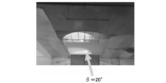
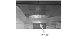
- the light guiding device includes a portion having a gentle curvature, and this portion is disposed, for example, under a tile, under a central ridge of the roof, in a window frame or crosspiece or the like.
- this invention is Having at least one photoelectric conversion device attached to the outer surface,
- the photoelectric conversion device is An optical waveguide device, And a photoelectric conversion unit provided in the light emitting unit of the optical waveguide device,
- the above optical waveguide device is A waveguide core layer, And a cladding layer covering the waveguide core layer discontinuously, The cladding layer is apart from the end of the disconnection portion not covering the waveguide core layer and the waveguide core layer opposite to the waveguide direction of the waveguide core layer with respect to the disconnection portion.
- the optical waveguide device is provided such that a light introducing core layer covered with the cladding layer is joined to the waveguide core layer at the disconnection portion of the cladding layer
- the electronic device may be a photoelectric conversion device in which light incident on a light incident portion of the optical waveguide device is emitted from the light emitting portion of the optical waveguide device and is incident on the photoelectric conversion portion.
- the electronic device may be basically anything, including both portable and stationary devices, but specific examples include mobile phones, mobile devices, robots, personal computers , In-vehicle devices, various home electric appliances, etc.
- the photoelectric conversion device is, for example, a solar cell used as a power supply of these electronic devices.
- this invention is Having at least one photoelectric conversion device attached to the outer surface,
- the photoelectric conversion device is An optical waveguide device, And a photoelectric conversion unit provided in the light emitting unit of the optical waveguide device,
- the above optical waveguide device is A waveguide core layer, And a cladding layer covering the waveguide core layer discontinuously, The cladding layer is apart from the end of the disconnection portion not covering the waveguide core layer and the waveguide core layer opposite to the waveguide direction of the waveguide core layer with respect to the disconnection portion.
- the optical waveguide device is provided such that a light introducing core layer covered with the cladding layer is joined to the waveguide core layer at the disconnection portion of the cladding layer,
- the moving body is a photoelectric conversion device in which light incident on a light incident portion of the optical waveguide device is emitted from the light emitting portion of the optical waveguide device and is incident on the photoelectric conversion portion.
- the moving body may be basically anything, but specific examples are a car, a two-wheeled vehicle, an aircraft, a rocket, a spacecraft, a ship, and the like.
- the photoelectric conversion device is, for example, a solar cell used as a power source of these moving bodies.
- the conventional waveguide has space inversion symmetry with respect to the traveling direction and the opposite direction (when viewed from the position where the start point and the end point are considered to be left and right (referred to as the viewpoint S), it has a symmetrical structure).
- the waveguide process is a process according to Maxwell's equation, it has time reversal symmetry. Now, assuming that three-dimensional propagation light (from the outside for the waveguide) emitted from the viewpoint S can enter this waveguide structure (two-dimensional waveguide) through a certain structure D.
- the other half to the right and the other half to the left progress toward the right (the light toward the right is incident on the photoelectric conversion unit at the end, for example, a solar cell to generate power). Since there is time reversal symmetry, when the direction of time is reversed, light travels leftward in the two-dimensional waveguide from the photoelectric conversion unit, passes through the structure D, and emerges outside and returns to the viewpoint S. .
- the problem is that, even when time is normal, half of the light incident to the left can be present due to the space inversion symmetry. This light is transmitted outside through structure D (which exists everywhere between the start point and the end point, assuming that outside light is taken in the two-dimensional waveguide everywhere in the start point and the end point) come.
- the light introduced from the outside comes into contact with the waveguide core layer coming from the left and the light introducing core layer tangentially, As described above, it is possible to collect light from the outside even in the middle of the start point and the end point by being guided all in the right direction by becoming one in the more right region).
- the time reversal of this process means that light that temporarily travels from right to left in the structure will flow out all over the waveguide (conversely, it is used to solve the problem of sunshine right) In the north face of the building, this arrangement will incorporate wall materials incorporating the optical waveguide device of the present invention).
- the solar cell coupled at the end point the photoelectric conversion element has a very small reflectance with respect to light incidence (for example, the particle diameter gradually increases on the surface) It goes without saying that it is extremely important and effective to set (due to such a structure as accumulated particles).
- this invention is A waveguide core layer, And a cladding layer covering the waveguide core layer discontinuously,
- the cladding layer is apart from the end of the disconnection portion not covering the waveguide core layer and the waveguide core layer opposite to the waveguide direction of the waveguide core layer with respect to the disconnection portion.
- Extending between and gradually approaching the guiding core layer towards the guiding direction of the guiding core layer, and a tangent at the end of the break parallel or substantially parallel to the guiding core layer It has a structure provided parallel to its part,
- the electromagnetic wave guiding device or the antenna device is provided such that the electromagnetic wave introducing core layer covered with the cladding layer is joined to the waveguide core layer at the disconnection portion of the cladding layer.
- This electromagnetic wave waveguide device is intended for electromagnetic waves of a wide range of wavelengths, and includes the above-described optical waveguide device which condenses and guides light.
- the electromagnetic waves are typically microwaves or terahertz waves (wavelength 30 cm to 0.3 cm, frequency 1 GHz to 1 THz), but are not limited thereto.
- the cladding layer is formed of a material that reflects electromagnetic waves, typically a metal, and the waveguide core layer and the electromagnetic wave introducing core layer are transparent to electromagnetic waves, specifically a dielectric. It is formed by The dielectric also includes air.
- the electromagnetic wave collected by the electromagnetic wave waveguide device and guided through the waveguide core layer is extracted from the waveguide core layer to the outside, and converted into a direct current by a rectifier circuit using a semiconductor element such as a diode, for example, and an electrical device It is used for etc.
- the electromagnetic wave waveguide device also plays a role as an antenna for receiving an electromagnetic wave.
- This electromagnetic wave waveguide device can be used for various buildings, electronic devices, and moving bodies as in the above-described light waveguide device.
- the optical waveguide device since the optical waveguide device has an asymmetrical structure with respect to the waveguide direction of the waveguide core layer and the opposite direction, the light is incident on the light incident surface of the optical waveguide device and introduced from the light introducing core layer.
- the light which has joined the waveguide core layer is efficiently guided in the waveguide direction in the inside of the waveguide core layer in a predetermined waveguide direction and emitted from the optical waveguide device.
- This optical waveguide device can efficiently condense light incident from the outside, and can efficiently conduct light without causing loss in the middle of the waveguide core layer.
- the light in the guiding core layer is guided 100% along the guiding direction, but due to the discontinuity of the cladding layer and the quasi-releasing property of the guiding core layer, the light to the guiding core layer is Can be taken from the beginning to the end of the waveguide core layer (with discrete continuity), ie at multiple points in the waveguide direction. And for the purpose of light condensing and highly efficient wave guiding, extremely effective structure and function can be realized.
- the photoelectric conversion device for example, by combining the above-described optical waveguide device with a multistripe photon photo carrier orthogonal photoelectric conversion device, it becomes possible to realize high photoelectric conversion efficiency approaching the thermodynamic limit. Furthermore, it is possible to combine this optical waveguide device with a conventional tandem solar cell, and it is possible to perform photoelectric conversion corresponding to the continuous spectrum of sunlight with higher efficiency than before. In particular, by providing this optical waveguide device in combination with a waveguide core layer having a surface structure such that incident light is guided into a glass surface, the windows and walls of a conventional building can achieve high efficiency. A photon / photo carrier orthogonal photoelectric conversion device can be obtained. In combination with solar cell applications, it is also useful as an exterior wall material for buildings that can be "dressed with light.”
- the net traveling direction of light guided in the waveguide core layer and the net carrier generated in the semiconductor layer by the light incident on the semiconductor layer from the end face of the waveguide core layer By making the angle ⁇ with the moving direction substantially perpendicular, it is possible to achieve both the maximization of the light absorption amount by the selection of the thickness of the semiconductor layer in the light incident direction and the minimization of the inter-electrode distance. Therefore, extremely high photoelectric conversion efficiency can be obtained.
- the light incident on the light incident surface of the optical waveguide device is guided in the waveguide core layer to be incident on the semiconductor layer, it is possible to prevent the light from being directly incident on the semiconductor layer.
- the semiconductor layer is made of, for example, amorphous silicon or an organic semiconductor, it is possible to suppress the deterioration of the organic semiconductor due to the Steffler-Ronski (SW) effect or the ultraviolet component. Further, by increasing the area of the light incident surface of the optical waveguide device, it is extremely easy to increase the area of the photoelectric conversion device.
- the band gap of the semiconductor layer or the semiconductor layer is made of an organic semiconductor, the HOMO-LUMO gap decreases stepwise and / or continuously in the incident direction of light, whereby the main part of the solar light spectrum Alternatively, light of all wavelengths can be absorbed for photoelectric conversion, and ultimately, photoelectric conversion efficiency approaching the theoretical maximum efficiency can be obtained.
- the characteristics of almost all conventional solar cells can be improved by raising the output voltage.
- the solar cell unit can be prevented from being exposed to the open air, the useful life of the solar power generation system can be increased. This is useful not only for the earth, but also for space, as well as for improving the reliability of solar cell systems that are power sources such as space stations, artificial satellites, and planetary probes.
- it is expected to be useful for alleviating the so-called sunshine issue by enabling light to be transported to the back side of the building by using it for the side wall of the building, and for the light transportation to the area that has been a shadow of conventional buildings. .
- this structure is interwoven to make clothes-type sun protection clothes (and solar power generation clothes), tents, and large-scale cloth-like structures.
- Solar power generation can be performed while exuding artisticity while covering buildings and buildings of bridges.
- Application as clothes is also possible. Fiber, fiber and textile applications are realized.
- the electromagnetic wave waveguide device can obtain the same effect as that of the above-described optical waveguide device for the whole electromagnetic wave.
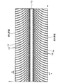
- FIG. 1 is a cross-sectional view showing an optical waveguide device according to a first embodiment of the present invention. It is sectional drawing which expands and shows the disconnection part vicinity of the cladding layer of the optical waveguide apparatus by 1st Embodiment of this invention. It is sectional drawing which expands and shows the disconnection part vicinity of the cladding layer of the optical waveguide apparatus by 1st Embodiment of this invention.
- FIG. 7 is a cross-sectional view showing an example of a method of manufacturing the optical waveguide device according to the first embodiment of the present invention.
- FIG. 7 is a cross-sectional view showing an example of a method of manufacturing the optical waveguide device according to the first embodiment of the present invention.
- FIG. 1 is a cross-sectional view showing an optical waveguide device according to a first embodiment of the present invention. It is sectional drawing which expands and shows the disconnection part vicinity of the cladding layer of the optical waveguide apparatus by 1st Embodiment of this invention.
- FIG. 7
- FIG. 7 is a cross-sectional view showing an example of a method of manufacturing the optical waveguide device according to the first embodiment of the present invention.
- FIG. 7 is a cross-sectional view showing an example of a method of manufacturing the optical waveguide device according to the first embodiment of the present invention.
- It is a top view which shows an example of the planar shape of the optical waveguide apparatus by 1st Embodiment of this invention.
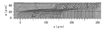
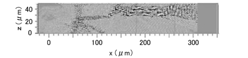
- It is a schematic diagram which shows the structure used for the simulation performed in order to verify the waveguide performance of a waveguide core layer in the optical waveguide apparatus by the 1st Embodiment of this invention.
- FIG. 1 It is a schematic diagram which shows the result (structure and light field) of the simulation performed in order to verify the waveguide performance of the optical waveguide apparatus by 2nd Embodiment of this invention. It is a basic diagram which shows the result (light field) of the simulation performed in order to verify the waveguide performance of the optical waveguide apparatus by 2nd Embodiment of this invention.
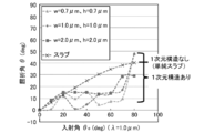
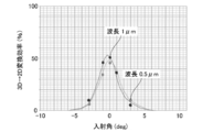
- a substantially line indicating conversion efficiency of two-dimensional guided light of wavelengths 1 ⁇ m and 0.5 ⁇ m incident on an optical waveguide device according to a second embodiment of the present invention with respect to the incident angle of the three-dimensional incident light FIG. It is sectional drawing which shows the optical waveguide apparatus by 3rd Embodiment of this invention.
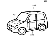
- FIG. 11 It is a side view showing an optical waveguide device according to an eleventh embodiment of the present invention. It is a perspective view showing an automobile according to a twelfth embodiment of the present invention.
- FIG. A schematic diagram showing the results (light field) of a simulation performed to verify the waveguide performance of the optical waveguide device portion of the photoelectric conversion device installed on the hood and roof of a car according to the twelfth embodiment of the present invention It is.
- FIG. 16 is a schematic diagram showing the results (introduction efficiency) of a simulation performed to verify the waveguide performance of the optical waveguide device portion of the photoelectric conversion device installed on the hood and roof of an automobile according to the twelfth embodiment of the present invention It is.
- An approximate line showing a result (structure and light field) of a simulation performed to verify the waveguide performance of the electromagnetic wave waveguide device of the electromagnetic wave power receiving device installed in the front door of the automobile according to the twelfth embodiment of the present invention
- FIG. This is a schematic diagram showing the result (light field) of a simulation carried out to verify the waveguide performance of the electromagnetic wave waveguide device of the electromagnetic wave power receiving device installed in the front door of a car according to the twelfth embodiment of the present invention. is there.
- FIG. 12 is a schematic diagram showing the results (introduction efficiency) of a simulation performed to verify the waveguide performance of the electromagnetic wave waveguide device of the electromagnetic wave power receiving device installed in the front door of a car according to the twelfth embodiment of the present invention is there.
- It is a schematic diagram which shows arrangement
- FIG. 1 A schematic view showing the results (structure and light field) of a simulation performed to verify the waveguide performance of an optical waveguide device portion of a photoelectric conversion device installed on a hood and a roof of an automobile according to a twelfth embodiment of the present invention
- FIG. A schematic diagram showing the results (light field) of a simulation performed to verify the waveguide performance of the optical waveguide device portion of the photoelectric conversion device installed on the hood and roof of a car according to the twelfth embodiment of the present invention It is.
- 16 is a schematic diagram showing the results (introduction efficiency) of a simulation performed to verify the waveguide performance of the optical waveguide device portion of the photoelectric conversion device installed on the hood and roof of an automobile according to the twelfth embodiment of the present invention It is.
- It is a schematic diagram which shows arrangement
- FIG. 16 is a schematic diagram showing the results (introduction efficiency) of a simulation performed to verify the waveguide performance of the optical waveguide device portion of the photoelectric conversion device installed on the hood and roof of an automobile according to the twelfth embodiment of the present invention It is. It is sectional drawing which shows the optical waveguide apparatus by 13th Embodiment of this invention.
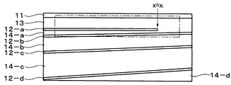
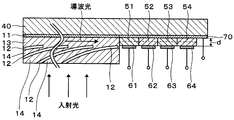
- FIG. 1 shows an optical waveguide device according to a first embodiment.
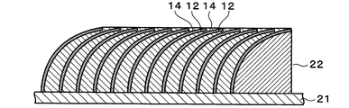
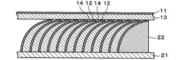
- the upper and lower sides of a flat waveguide core layer 13 are sandwiched between the cladding layer 11 and a plurality of cladding layers 12 periodically arranged at an interval ⁇ in the waveguide direction.
- the cladding layer 11 covers one main surface (upper surface) of the waveguide core layer 13 continuously
- the cladding layer 12 covers the other main surface (lower surface) of the waveguide core layer 13 discontinuously.
- the cladding layer 11 and the cladding layer 12 collectively constitute a cladding layer that covers the waveguide core layer 13 discontinuously.
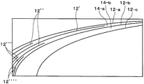
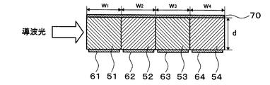
- this cladding layer has an end (for example, indicated by E in FIG. 1) of the disconnection portion not covering the waveguide core layer 13 and the waveguide direction of the waveguide core layer 13 with respect to this disconnection portion. And a position (for example, indicated by P in FIG. 1) opposite to the waveguide core layer 13 and directed toward the waveguide direction of the waveguide core layer 13. , And has a structure in which a tangent at the end of the break portion is parallel or almost parallel to the waveguide core layer 13 as described later. Both side surfaces of the waveguide core layer 13 may be covered by the extension of the cladding layer 11 or may be constituted by a reflecting surface. The detail of the coupling portion between the cladding layer 12 and the waveguide core layer 13 is shown in FIG.
- the cladding layer 12 is indicated by cladding layers 12-a, 12-b, 12-c and 12-d.
- a light introducing core layer 14 is provided between each cladding layer 12 and the adjacent cladding layer 12.
- the light introducing core layer 14 is indicated by light introducing core layers 14-a, 14-b, 14-c and 14-d.
- the cladding layer 12 and the light introducing core layer 14 extend a predetermined distance in the vertical direction (depth direction) of FIG.
- the cladding layer 12 has a concavely curved shape in the waveguiding direction of the waveguide core layer 13, and the shape is selected as necessary.
- FIG. 1 the cladding layer 12 is indicated by cladding layers 12-a, 12-b, 12-c and 12-d.
- a light introducing core layer 14 is provided between each cladding layer 12 and the adjacent cladding layer 12.
- the light introducing core layer 14 is indicated by light introducing core layers 14-a, 14-b, 14-c and 14-d.
- the cladding layer 12 has a quarter circle. The case of having a shape is shown.
- the tangent of the end of the cladding layer 12 on the side of the waveguide core layer 13 coincides with the plane of the waveguide core layer 13 and thus coincides with the waveguide direction in the waveguide core layer 13.
- the end on the waveguide core layer 13 side of the cladding layer 12 is tangentially connected to the waveguide core layer 13.
- the refractive indices of the cladding layers 11 and 12 and the waveguide core layer 13 are cladding relative to the refractive index of the waveguide core layer 13 so that light can be confined in the waveguide core layer 11 by the cladding layers 11 and 12
- the refractive index of the layers 11, 12 is chosen small.
- the refractive index of the cladding layer 12 and the light introducing core layer 14 is different from that of the cladding layer 12 with respect to the refractive index of the light introducing core layer 14 so that light can be confined in the light introducing core layer 14 by the cladding layer 12.
- the refractive index of is chosen small.
- the refractive index of the waveguide core layer 13 and the refractive index of the light introducing core layer 14 are preferably selected to be equal, but are not limited thereto.
- the planar shape of the optical waveguide device is not particularly limited and may be appropriately selected depending on the application of the optical waveguide device. For example, it is rectangular or square, and in this case, the optical waveguide device has a rectangular parallelepiped shape as a whole.
- the cladding layer 12 having the above-mentioned quarter circle cross-sectional shape has a perpendicular light incident surface (bottom surface of the optical waveguide device) as a tangent.
- the cladding layer 12 breaks off and has a horizontal tangent there.
- the waveguide core layer 13 portion with a large refractive index
- FIG. 12 It is characterized in that it is not closed off in the cladding layer 12 and has a geometrically open structure. Thereby, as shown in FIG.
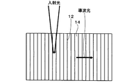
- the x-axis is taken in the waveguide direction (the z-axis is taken in the thickness direction of the optical waveguide device and the y-axis is taken in the direction perpendicular to the paper of FIG. 1)
- x ⁇ x i in the vicinity of the waveguide core layer 13 and its lower portion, as shown in FIG.
- the waveguide core is taken from the outer world other than the start point (through the light introducing core layer 14a from the lower left side in FIG. Light can penetrate layer 13.
- the light introducing core layer 14-c) (branch) joins the waveguide core layer 13 (main stream) (in FIG.
- the light introducing core layer existing below the light introducing core layer 14-c and The cladding layer between the light introducing core layer and the light introducing core layer 14-c is not shown).
- the tangent (indicated by a broken line in the figure) at the right end (break) of the cladding layers 12-a, 12-b and 12-c is parallel or almost parallel to the traveling direction of the guided light. It has become. That is, tangential connections are made to the waveguide core layer 13 at the end portions of the cladding layers 12-a, 12-b and 12-c. In this way, the waveguide core layer 13 is given continuous translational symmetry along the advancing method as shown by the thick arrows in FIG. Give it a sex.
- the waveguide core layer 13 has a quasi-release structure.
- Another lower cladding layer 12-b closer to the waveguide core layer 13 covers the disconnection of the closest cladding layer and also becomes the closest cladding layer by itself. Light is efficiently guided to the right in FIG. 3 without loss.
- each discontinuous cladding layer 12 has a geometry in which its tangent line is parallel (horizontal) or almost parallel to the waveguide core layer 13 at its upper end (as shown by the broken line in FIG. 3).
- the above-mentioned "parallel or nearly parallel” is defined by being parallel to such an extent that total reflection can occur by the above process. Due to this parallelism, as described above, the light in the waveguide core layer 13 is efficiently guided approximately 100% without being dissipated.
- the same applies to the cladding layer 12-b and the cladding layer 12-c at x x i + ⁇ . The same applies to all the main stream and tributary junctions thereafter.
- Examples of the material of the waveguide core layer 13 include, but are not limited to, inorganic substances having a refractive index of about 1.6 to 2.0, inorganic glass, high refractive index resins having a refractive index of 1.6 or more, and the like. It is not something to be done.
- Examples of the material of the light introducing core layer 14 include inorganic materials having a refractive index of about 1.6 to 2.0, inorganic glass, high refractive index resins having a refractive index of 1.6 or more, and the like. (Especially when using an air layer or the like as a cladding layer sandwiching the same layer).
- a resin that can obtain a low refractive index such as a refractive index of 1.34, for example, CYTOP in addition to this, it is also possible to use an air layer.
- the refractive index of the waveguide core layer 13 and the light introducing core layer 14 and the refractive index of the cladding layers 11 and 12 is 2.0
- the refractive index of the cladding layers 11 and 12 is 1.35.
- the enlargement of the optical waveguide device becomes easy, so When an increase in area is required, it is also conceivable to set the refractive index of the waveguide core layer 13 and the light introducing core layer 14 to about 1.6 and the refractive index of the cladding layers 11 and 12 to 1.35.
- This optical waveguide device can be used, for example, by bonding it to a building window material with the cladding layer 11 down.
- a conventional surface-incidence type solar cell as a photoelectric conversion portion in the light emitting portion of the optical waveguide device to constitute a photoelectric conversion device, solar power generation can be facilitated in the window material for construction It can be realized.
- the thickness of the cladding layers 11 and 12 is, for example, 1 ⁇ m or more and several ⁇ m or less (for example, 2 ⁇ m or less), but is not limited thereto.
- the thickness of the waveguide core layer 13 is in the order of 1 ⁇ m to 1 mm. However, in the application installed on the outer wall of a building, several mm may be used.
- the thickness of the waveguide core layer 13 in the case where this optical waveguide device is coupled to a photon photo carrier orthogonal type solar cell in which light is incident in parallel to the pn junction is about 2 ⁇ m to 300 ⁇ m or about 2 ⁇ m to about 300 ⁇ m.
- the value of 1 / c is larger than that of the conventional waveguide of the same size for the waveguide of the optical waveguide device as a whole by one digit or more.
- This makes it possible to introduce light from the external world anywhere between the start point and the end point of the waveguide core layer 13, so that a region having the same refractive index as the waveguide core layer 13, that is, the light introducing core layer 14. Is continuous to the edge of the waveguide core layer 13 and the total extension (segments of the cross section) of the cladding layer 12 present at the edge of this region and contributing to light introduction from the outside is much longer. .
- each part of the optical waveguide device is appropriately selected according to the purpose of use of the optical waveguide device, for example, the width in the x-axis direction in FIG. 1 is 5 cm to 100 cm and the thickness in the z axis direction is 1 mm to 6 mm.
- the depth (the width in the y-axis direction) is 3 cm to 50 cm
- the shape of the curve of the cladding layer 12 is a quarter circle having a radius of 6 mm.
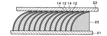
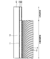
- an alternate laminated film of a cladding layer 12 made of thermoplastic resin and a light introducing core layer 14 is formed on a substrate 21, and a mold 22 is formed on the substrate 21 to be in contact with this alternate laminated film. While fixing, the push plate 23 is placed on this alternate laminated film.
- the mold 22 has a quarter-circle shaped cross-section and extends vertically in FIG. 4A. The arc length of the mold 22 is selected to be the same as the height of the alternate laminated film.
- the push plate 23 is pushed down to hit the mold 22 horizontally.
- the alternately laminated film forms a curved structure.
- the cladding layer 12 and the light introducing core layer 14 forming the alternately laminated film deform following the mold 22.
- the lateral shifting is performed so that the height of the alternate lamination film before compression and shear matches the length of the arc of the mold 22 after compression and shear, and the cladding layer 12 and the light
- the width of the introduction core layer 14 in the direction parallel to the substrate 21 can also be maintained before and after compression and shear. Since the width is constant regardless of the height, the periodic arrangement structure with the spacing ⁇ of the cladding layers 12 shown in FIG. 1 becomes possible.
- “+ shear” the end of the light introducing core layer 14 is narrowed
- ⁇ shear relatively thickened the end of the light introducing core layer 14
- FIG. 4C Thereafter, as shown in FIG. 4C, the pressure plate 23 is removed, and the waveguide core layer 13 provided with the cladding layer 11 on the upper surface is pressure-bonded thereon to complete the structure shown in FIG. 4D.
- a black line is drawn between the waveguide core layer 13 and the light introducing core layer 14 for convenience of illustration, but in practical use, since the black line is typically made to have the same refractive index, the black line is actually Note that it does not exist).
- the shape of the curve of the mold 22 may be matched to the curved shape.
- the shape of the curve of the mold 22 it is possible to form an ellipse, other significant curves, an inflection point structure, and the like.
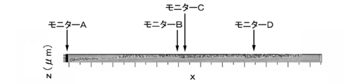
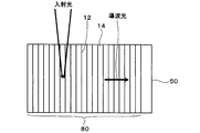
- FIG. 5 shows a view of the optical waveguide device having a rectangular planar shape as viewed from the light incident surface side. As shown in FIG. 5, consider the case where incident light is incident from the outside in a direction substantially perpendicular to the light incident surface (light introducing surface) of the optical waveguide device.
- each light introducing core layer 14 on the light incident surface is guided in the light introducing core layer 14 while being repeatedly totally reflected at the interface between the light introducing core layer 14 and the cladding layer 12 Then, the light is guided in the direction of the arrow in the waveguide core layer 13 and emitted from the end face of the waveguide core layer 13.
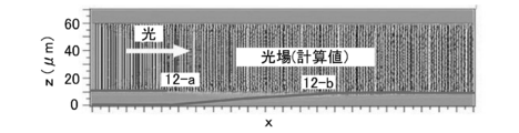
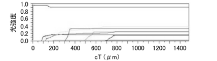
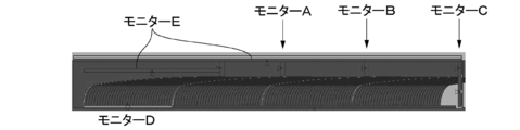
- FIG. 6A is an enlarged view of the confluence portion of the waveguide core layer 13 (main flow) of FIG. 2 and the light introducing core layer 14-a (which is simply described as a tributary in FIG. 6A).
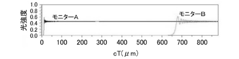
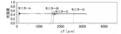
- monitors A and B for light intensity measurement are arranged at the positions shown in the figure.
- the triangle in FIG. 6A indicates the direction of light.
- the calculation results of the light intensity in the monitors A and B are shown in FIG. 6C.
- the horizontal axis in FIG. 6C is the product of the speed of light c and the time T, that is, the distance.
- the light intensities in the monitors A and B match, which means that the waveguide core layer 13 is a quasi-release system and the cladding layer 12 is discontinuous.
- the guiding core layer 13 is not formed at the upper end of the non-continuous cladding layer 12 described above.
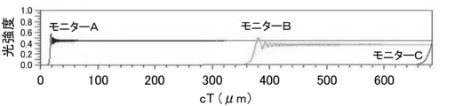
- FIG. 7A is an enlarged view of a junction of the waveguide core layer 13 of FIG. 2 and the light introducing core layer 14-a (denoted as a light introducing core layer (triple flow) in FIG. 7A).
- the monitors A, B, and C are disposed in the light introducing core layer 14-a and the waveguide core layer 13.
- the light intensity at the position A at the left end of the light introducing core layer 14-a in FIG. 7A, the light intensity at the position B immediately after merging, and the light intensity at the position C at the right end of the waveguide core layer 13 are shown in FIG. . As shown in FIG.
- the light intensities in the monitors A, B, and C are substantially the same, and the waveguide core layer 13 is a quasi-release system and the cladding layer 12 is discontinuous.
- Light is injected into the waveguide core layer 13 which is the main flow from -a, and the position C of the waveguide core layer 13 without loss from the position A of the light introducing core layer 14-a far from the junction point It can be seen that the light is guided almost 100%.
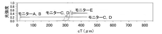
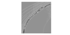
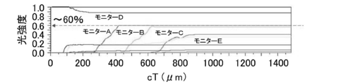
- FIGS. 8A, 8B and 8C show simulation results of merging (multiplexing) of the light guided in the waveguide core layer 13 and the light guided in the light introducing core layer 14-a.
- FIG. 8A is an enlarged view of the junction of the waveguide core layer 13 and the light introducing core layer 14-a.
- the monitor A is disposed in the waveguide core layer 13
- the monitor B is disposed in the light introducing core layer 14-a
- the monitor C is disposed downstream of the waveguide core layer 13
- the monitor D is disposed at a position corresponding to the monitor C of a
- the monitor E is disposed downstream of the monitor C of the waveguide core layer 13.
- FIG. 8C The result of having evaluated the light intensity in monitor A, B, C, D, E of FIG. 8A is shown to FIG. 8C. As shown in FIG.
- the light intensities in monitors A and B substantially match the light intensities in monitors C and D
- the light intensities in monitor E are the light intensities in monitors A and B and those in monitors C and D.
- the waveguide core layer 13 is a quasi-release system and the cladding layer 12 is discontinuous because it is equal to the sum with the light intensity. It can be seen that light is guided 100% without loss to the position of the monitor C after the merging of the waveguide core layer 13 and the light introducing core layer 14-a.
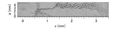
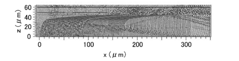
- FIGS. 9A and 9B show the appearance of a slightly global waveguide (three junctions along the waveguide core layer 13 in FIG. 1) Calculation results in the case of including one) are shown in FIGS. 9A and 9B.
- the light was introduced from the light introducing core layer 14 which is a branch, reflecting that the light was taken in from the outside.
- FIG. 9A shows a state of waveguiding in the optical waveguide device of light emitted from the left end of the branch.
- the evaluation result of the light intensity in monitor A, B, C, D of FIG. 9A is shown to FIG. 9B. As shown in FIG.
- the optical waveguide device since the optical waveguide device has an asymmetric structure with respect to the waveguide direction of the waveguide core layer 13 and the opposite direction, the light is incident on the light incident surface.
- the light introduced from the light introducing core layer 14 and joined to the waveguide core layer 13 is efficiently guided in the waveguide direction of the inside of the waveguide core layer 13 in a predetermined waveguide direction and emitted from the optical waveguide device .
- This optical waveguide device can efficiently condense light incident from the outside, and can efficiently guide light without causing loss in the middle of the waveguide core layer 13.
- the waveguide core Light can be introduced into the layer 13 from the start point to the end of the waveguide core layer 13, ie at a plurality of points in the waveguide direction. And for the purpose of light condensing and highly efficient wave guiding, extremely effective structure and function can be realized.
- three-dimensional space propagation light incident on the light incident surface of the optical waveguide device is introduced into the light introducing core layer 14, and while being totally reflected repeatedly in the light introducing core layer 14, the light is made incident on the waveguide core layer 13.
- This optical waveguide device can be applied to a wide range of fields, such as a highly efficient light receiver, a light receiving image transfer / reproducer, and the like.
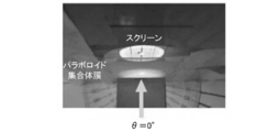
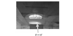
- FIG. 10 shows an optical waveguide device according to a second embodiment. As shown in FIG. 10, this optical waveguide device has the same configuration as that of the optical waveguide device according to the embodiment of the first embodiment except that the light wave traveling direction changing layer 35 is provided on the light incident surface. Have.
- the light wave traveling direction conversion layer 35 has a direction perpendicular to the surface of the light wave traveling direction conversion layer 35 regardless of the incident angle of the incident light incident on the light wave traveling direction conversion layer 35. Can be converted to light. For this reason, even if incident light enters the optical waveguide device from various directions, the traveling direction is converted into the direction perpendicular to the light incident surface by the light wave traveling direction conversion layer 35, and as a result, the light introducing core Light can be introduced into the inside of the waveguide core layer 13 while repeating total reflection in the layer 14.
- the refractive index of the said transparent resin was 1.52.
- a light (plane wave) having a wavelength of 1.0 ⁇ m was made incident on this one-dimensional structured slab waveguide at an incident angle ⁇ 0 ( ⁇ 30 °).
- FIG. 11 shows the distribution of the magnitude (intensity) of the amplitude E y in the y-axis direction of the electric field of the light wave in the xz plane. It can be seen from FIG. 11 that light incident on this one-dimensional structured slab waveguide at an incident angle ⁇ 0 is transmitted from this one-dimensional structure, and then enters from a direction substantially perpendicular to the slab waveguide. . That is, it is understood that the L & S structure can convert the traveling direction of the obliquely incident light into a direction substantially perpendicular to the surface of the light wave traveling direction conversion layer 35.
- FIG. 12 shows the results of simulation of changes in the refraction angle (effective refraction angle) with respect to the incident angle ⁇ 0 by changing the width w and height h of the structure of the parabola cross section constituting the one-dimensional structure.
- the same result when using a simple slab waveguide without a one-dimensional structure is also shown in FIG.
- the vertical incidence approaches compared with the case where a mere slab waveguide is used, the vertical incidence approaches (effective refraction angle is suppressed to about 0 ° ⁇ 10 °) through the L & S structure composed of a parabolic cross-section structure. I understand.
- the cross-sectional shape is a parabola having a rotational symmetry about the axis, that is, a film (paraboloid aggregate film) formed of an assembly of paraboloids (paraboloid) is also used as the light wave traveling direction changing layer 35 It is valid.
- FIG. 14A and 14B show that when the light wave traveling direction changing layer 35 is used in a two-layer tandem, the three-dimensional incident light is two-dimensionally guided when the three-dimensional incident light (3D) is vertically incident on the incident surface of the optical waveguide device.
- FIG. 14A shows the structure of the cladding layer 12 and the light introducing core layer 14 in addition to the light field in the optical waveguide device
- FIG. 14B shows the state of conversion to wave light (2D). Only the light field is displayed.
- the structure of the light introducing portion has translational symmetry in the depth direction with respect to the paper surface (the cross-sectional structure is shown in FIG. 14A).
- This light introducing part has discrete translational symmetry along the x-axis direction, and the light from directly below is vertically elongated oval (in this example, 11 ⁇ m short axis, 22 ⁇ m long axis, light receiver [receiver] part) And a horizontal oblong ellipse connected at the top of this ellipse (in this example, the minor axis is 30 ⁇ m, the major axis is 180 ⁇ m, and it is called a light merger part).
- the light merger ellipse merges tangentially with the waveguide core layer 13 at its top.
- the top of the light receiver ellipse (the connection point with the light merger ellipse) is set to be located 8 ⁇ m below the lower end of the waveguide core layer 13.
- the width of the light introducing core layer 14 is about 2.25 ⁇ m at the lower end incident surface (along the x-axis direction) and the width of the cladding layer 12 is 0.4 ⁇ m, but the width of the cladding layer 12 is 1 ⁇ m every 32 cycles.
- the light introducing core layer 14 has a discrete translational symmetry which is thickened along the x-axis direction. The wavelength used for the calculation is 1 ⁇ m. As shown in FIGS.
- FIG. 15 shows the relationship between the conversion efficiency of the three-dimensional incident light to the two-dimensional guided light and the incident angle for the cases where the wavelength is 1 ⁇ m and 0.5 ⁇ m. From FIG. 15, the conversion efficiency of three-dimensional incident light into two-dimensional guided light (that is, the efficiency of introducing light into the waveguide core layer 13 in FIGS. 1 to 3) is approximately 50% at an incident angle near 0 °. It can be seen that the wavelength dependence of the conversion efficiency is small. The wavelength dependency of the conversion efficiency is small because a reflection optical system is used in this optical waveguide device.
- the sunlight is substantially perpendicular to the light incident surface of the optical waveguide device regardless of the incident angle of light to the optical waveguide device.
- the deviation from the normal incidence can be suppressed to about 8 degrees or less.
- the paraboloid aggregate film is used for the light wave traveling direction changing layer 35, as can be seen from FIGS. 13A to 13I, the deviation from the vertical incidence can be suppressed to substantially the same degree.
- incident light can be vertically incident on the light incident surface of the optical waveguide device by the light wave traveling direction conversion, and the light of this incident angle has the structure of FIG. 10 (for example, the waveguide core layer 13 and the light introducing core Since the layer 14 has a refractive index of 2.0 and the cladding layers 11 and 12 have a refractive index of 1.35, the cladding layer 12 is orthogonal to the light incident surface because it is a quarter circle. It should be noted that it is totally reflected. In this manner, light can be efficiently introduced into the waveguide core layer 13 through the light introducing core layer 14, and the amount of light guided inside the waveguide core layer 13 can be significantly increased. You can get the advantage of being able to
- FIG. 16A shows an optical waveguide device according to the third embodiment, and in particular, schematically shows an example of the light introducing core layer 14 and the cladding layer 12 having high light introducing efficiency.
- the cladding layers 12 ′ and 12 ′ ′ are supplementarily included in the light introducing core layer 14-a sandwiched between the cladding layer 12-a and the cladding layer 12-b. , 12 ''',12''', etc. are provided. Although not shown, a similar structure is produced also in the light introducing core layer 14-b sandwiched between the cladding layer 12-b and the cladding layer 12-c, and including these layers, the whole is discrete in the x-axis direction Dynamic symmetry has been established.
- the auxiliary cladding layers 12 ′, 12 ′ ′,... are provided only in the middle of the light introducing core layer 14-a in the lengthwise direction, and the lengths and positions thereof are the above-mentioned effective crossing angles It can be quantitatively determined by the difference of angles formed by tangents at the same z-coordinate value.
- ( ⁇ / 2 ⁇ c ) / ⁇ is sufficiently large.
- 16B shows the results of a simulation conducted to verify the waveguide performance, but by means of the auxiliary cladding layers 12 ′, 12 ′ ′,..., Total internal reflection is repeated repeatedly within the light introducing core layer 14-a. However, when light is guided, the total reflection condition can be more easily satisfied over the entire length of the light introducing core layer 14-a.
- This is another example of tangential connection, in which light propagating in the core layers above and below the discontinuous cladding layer, microspherical waves according to the principle of Huygens, and the cladding above and below the interrupted cladding layer (auxiliary cladding layer) The inclinations of the tangents of the three cladding layers are substantially parallel to each other to such an extent that the layers are totally reflected.
- the (optical waveguide or light introduction) waveguide is generally (see FIG. 1). Not only a planar shape typified by the like, etc.), it may be generally gently curved as shown in FIG. 16A (which becomes a useful feature when attaching the optical waveguide device of the present invention to a car bonnet or the like).
- the other configuration of this optical waveguide device is the same as that of the optical waveguide device according to the form of the first embodiment.
- the width of the auxiliary cladding layer becomes narrower as it goes upward from the base portion of FIG. 16A, and the auxiliary cladding layer in FIG. It is also effective to adopt a structure (tapered structure) in which the width is smaller than the light penetration length and does not function as a cladding layer after the point at which the.
- the material itself constituting the auxiliary cladding layer can be arranged continuously without interruption from the base portion of FIG. 16A to the waveguide core layer 13 which is the main waveguide, which is easier.
- the above-described tapered structure can be realized by controlling the lateral displacement in accordance with the vertical position (z coordinate) of the figure (for example, to obtain a structure as shown in FIG. 14A).
- the amount of light reaching the waveguide core layer 13 from the light introducing core layer 14 can be increased.
- the advantage that the utilization efficiency of the light which injects into an apparatus can be aimed at can be acquired.
- FIG. 17 shows an optical waveguide device according to the fourth embodiment. As shown in FIG. 17, this optical waveguide device has the same configuration as the optical waveguide device according to the form of the first embodiment, except that the cladding layer 12 on the light incident surface side has a linear cross-sectional shape. Have.
- the cladding layer 12 in the range of the thickness t on the light incident surface side has a linear cross-sectional shape that makes an angle ⁇ with the light incident surface.
- the tangents of the shown quarter circles are connected at a position having an elevation angle of ⁇ from the horizontal direction.
- t ⁇ ⁇ tan ⁇ .
- the linear cladding layer 12 is made of a metal having a high light reflectance, such as aluminum, in addition to the low refractive index layer.
- the fourth embodiment in addition to the same advantages as those of the first embodiment, all the light incident perpendicularly to the light incident surface of the optical waveguide device is efficiently efficiently taken by the straight portion of the cladding layer 12 By reflecting the light, the light introducing core layer 14 can be guided and guided smoothly without causing loss anywhere between the start point and the end point, and the utilization efficiency of light incident on the light incident surface of the optical waveguide device The advantage that the improvement of can be aimed at can be acquired.
- FIG. 18 shows a photoelectric conversion device according to the fifth embodiment. As shown in FIG. 18, this photoelectric conversion device uses the optical waveguide device according to the first embodiment.
- this photoelectric conversion device has an optical waveguide device portion and a photoelectric conversion portion.
- the optical waveguide unit has the same structure as the optical waveguide unit shown in FIG.
- the photoelectric conversion unit may be various types of solar cells or photoelectric conversion elements, but FIG. 18 shows the case where the photoelectric conversion unit is formed of the semiconductor layer 50 for photoelectric conversion.
- a semiconductor layer 50 is provided on the substrate 40 provided on the cladding layer 11 and extending outside the waveguide core layer 13 in contact with the end face of the waveguide core layer 13.
- the substrate 40 can also play a role of mechanical support and mechanical protection of the optical waveguide device, and can play a role as a cladding layer for efficiently confining light inside the waveguide core layer 13 Alternatively, in this case, the clad layer 11 can also be used.
- the substrate 40 may have a multilayer structure of two or more layers.
- the substrate 40 is, for example, a glass plate, a transparent plastic plate, or the like.
- the transparent plastic constituting the transparent plastic plate examples include polyethylene terephthalate, polyethylene naphthalate, polycarbonate, polystyrene, polyethylene, polypropylene, polyphenylene sulfide, polyvinylidene fluoride, acetyl cellulose, brominated phenoxy, aramids, polyimides, polystyrene , Polyarylates, polysulfones, polyolefins and the like can be used.
- the substrate 40 may be flexible, and in this case, the photoelectric conversion device can be easily installed in a state of being bent along a convex surface or a concave surface.
- the semiconductor layer 50 has a pn junction, and the pn junction surface is parallel to the main surface of the waveguide core layer 13.
- the waveguide core layer 13 having a generally elongated rectangular planar shape and the semiconductor layer 50 are provided integrally with each other, and have a planar shape as a whole.
- a first electrode 60 and a second electrode 70 are provided on a pair of mutually opposing surfaces (upper surface and lower surface) of the semiconductor layer 50 on the upper and lower sides (with the light incident side up).
- One of the first electrode 60 and the second electrode 70 is used as an anode electrode, and the other is used as a cathode electrode.
- the first electrode 60 is used as an anode electrode
- the second electrode 80 is used as a cathode electrode.
- the first electrode 60 and the second electrode 70 may be provided for each region when the semiconductor layer 50 is divided into a plurality of regions made of semiconductors different from each other, and one of the first electrode 60 and the second electrode 70 may be provided on all the regions. It may be a full surface electrode extending to
- incident light three-dimensional space propagation light
- incident light three-dimensional space propagation light
- the light incident surface of the optical waveguide device portion is guided into the inside of the waveguide core layer 13 via the light introducing core layer 14
- the light is emitted from the end face of the waveguide core layer 13 and is incident on the semiconductor layer 50.
- the semiconductor layer 50 is obtained by the light traveling in the inside of the waveguide core layer 13 and the light incident on the semiconductor layer 50 from the end face of the waveguide core layer 13.
- the angle ⁇ between the net movement direction of the carriers (photocarriers) generated therein and the direction in which the first electrode 60 and the second electrode 70 are connected at the shortest distance is substantially perpendicular.
- the angle ⁇ is divided into a plurality of regions of the semiconductor layer 50 made of different semiconductors or the width of the light traveling direction of the first electrode 60, and the first electrode 60 is provided for each region. If the width of the first electrode 60 provided for each region is W ′ and the thickness of the semiconductor layer 50 is d, then ⁇ / 2 ⁇ ⁇ ⁇ ⁇ ⁇ / 2 + ⁇ (wherein , ⁇ ⁇ d / W ′), typically 80 ° ⁇ ⁇ ⁇ 100 °, most preferably 90 °.
- an antireflective film is preferably provided on the bonding surface between the waveguide core layer 13 and the semiconductor layer 50.
- a light shielding layer is provided above the semiconductor layer 50 so as to cover the first electrode 60.
- the light shielding layer can be selected from conventionally known ones, and is selected as necessary.
- an aluminum laminate film in which a plastic film is formed on both sides of an aluminum foil is used. The light shielding layer can prevent light from directly entering the semiconductor layer 50.
- the substrate 40 constitutes a part of the outer surface of a building or an electronic device
- sunlight is incident on the optical waveguide unit, but not incident on the semiconductor layer 50
- the semiconductor layer 50 is covered with a member or the like so as to be a shade.
- the window glass is the substrate 40
- the light waveguide device portion is provided on the window glass exposed to the outside. Make it hidden inside the frame.
- the end portions of adjacent photoelectric conversion devices are vertically overlapped, and the lower photoelectric conversion device is formed by the semiconductor layer 50 at the end portion of the upper photoelectric conversion device.
- the semiconductor layer 50 at the end of the semiconductor is covered.
- the transparent member on the surface of the display unit serves as the substrate 40, and the optical waveguide unit is provided on the transparent member exposed to the outside.
- the semiconductor layer 50 is concealed inside the member provided on the surface of the display unit.
- the semiconductor layer 50 is selected, for example, from those already mentioned as required.
- the semiconductor layer 50 is typically a pn junction composed of a p-type semiconductor layer and an n-type semiconductor layer.
- the portion of the semiconductor layer 50 in contact with the first electrode 60 and the second electrode 70 is doped to a high impurity concentration, and the first electrode 60 and the second electrode 70 serve as the semiconductor layer 50.
- the length of one side of the semiconductor layer 50 is typically selected to be the same as the length of the side of the waveguide core layer 13 on which the semiconductor layer 50 is provided, but the length of the side perpendicular to this side is typically And 0.5 ⁇ m to 5 mm, preferably 2 ⁇ m to 1 mm.
- the thickness of the semiconductor layer 50 is generally as small as several tens of ⁇ m or less, the volume of the semiconductor layer 50 is also extremely small. That is, the amount of use of the semiconductor layer 50 can be extremely small. Therefore, the manufacturing cost of the photoelectric conversion device can be reduced.
- Each of the regions 51, 52, 53, 54 has an elongated stripe shape extending in a direction parallel to the side of the waveguide core layer 13 on which the semiconductor layer 50 is provided.
- first electrodes 61, 62, 63, 64 are provided separately on the respective regions 51, 52, 53, 54, respectively.
- the second electrode 70 is a full surface electrode, and is a common electrode of each of the regions 51, 52, 53, 54. (The width in the traveling direction of light, the length of the lateral direction in FIG.
- E gi can be set as follows. For example, the wavelength is divided into N sections in the entire wavelength range of the AM 1.5 sunlight spectrum or the main wavelength range thereof (a range including a portion where the incident energy is high). Then, these sections are numbered in order from the short wavelength side (high energy side) as 1, 2, ..., N, and E gi is selected equal to the minimum photon energy of the i-th section. In this way, when a photon having photon energy of the kth section is incident on the Egi region, an electron-hole pair is generated to perform photoelectric conversion.
- the E gi from the junction surface of the waveguide core layer 13 and the semiconductor layer 50 Choose the distance to the area.
- the sunlight guided inside the waveguide core layer 13 and incident on the semiconductor layer 50 is first incident on the E g1 region, and one having a photon energy of E g1 or more in its spectrum is absorbed, It is converted, and then incident on the E g2 region, one of the spectra whose photon energy is greater than E g2 and smaller than E g1 is absorbed and photoelectrically converted, and finally enters the E gN region to be A photon energy of EgN or more and less than EgN-1 is absorbed and photoelectrically converted.
- light in substantially the entire range of the solar light spectrum or in the main wavelength range can be used for photoelectric conversion.
- each E gi can be performed by changing the semiconductor composition and a semiconductor in the form constituting each E gi region (amorphous, polycrystalline, single crystal) and the like.
- each Egi region is formed of another type of semiconductor.
- this semiconductor regardless of the magnitude of the absorption coefficient ⁇ , one having a high carrier mobility ⁇ can be selected, so the choice is wide.
- CdSe fine particles having an diameter of about 1.9 nm for E g1 region, CdSe fine particles (absorption peak wavelength 585 nm) for an E g2 region of about 4.0 nm, Eg3 region: PbSe fine particles of about 2 nm in diameter (absorption peak wavelength 800 nm), Eg4 region of about 4.5 nm in PbSe fine particles (absorption peak wavelength of 1100 nm), Eg5 region of about 90 nm in diameter PbSe fine particles (absorption peak wavelength of 2300 nm).
- E gi area when the N ⁇ 10 with only the control of x using GaInN x As 1-x and GaInN x P 1-x.
- it may be configured E gi region using the group II-VI compound semiconductor to exhibit significant bowing the inclusion of Te (bowing) is known. It will be as follows if the specific example about the case where an organic semiconductor and an inorganic semiconductor are used is given.
- halide organic-inorganic perovskite semiconductor (CH 3 NH 3 PbI 3 ) solar cell or CZTS using copper, zinc, tin or sulfur as a raw material at the end of the waveguide core layer 13.
- CIGS Cu, In, Ga, Se
- CZTSe Cu 2 ZnSnSe 4
- FIG. 1 Since bulk recombination in CZTS is considered to be the cause of performance degradation, the arrangement in which the light traveling direction and the photocarrier moving direction are orthogonal as shown in FIG.
- CTGS having copper, tin, germanium, and sulfur as constituent elements has a band gap of 1.0 eV, and is drawing attention as a material having a high light absorption coefficient and a nontoxic and nonrare element. Since the band gap can be adjusted by controlling the Ge / Sn ratio, it is promising as a photoelectric conversion element arranged in parallel connection in tandem at the end of the waveguide core layer 13 in FIG.
- the high-energy photon removal function that suppresses cohesion energy while effectively performing photoelectric conversion, as well as the above simple passivation, improves the reliability and prolongs the life of the organic semiconductor photoelectric conversion unit, which is also considered weak for outdoor use. It is also effective.
- this photoelectric conversion device is used as a solar cell, the length of the waveguide in the x direction is divided by the thickness of the solar cell, since the solar cell is a solar cell to which the waveguide core layer 13, ie, the waveguide is coupled. It is a highly efficient condensing system whose value is the condensing ratio.
- a solar cell for laser application is a system in which sunlight is converted to laser light (oscillation wavelength: approximately 1.06 ⁇ m) and this is emitted to a crystalline Si solar cell to generate electric power, and the thickness of the solar cell is only 50 ⁇ m
- laser light oscillation wavelength: approximately 1.06 ⁇ m
- the thickness of the solar cell is only 50 ⁇ m
- a high quantum efficiency of 0.8 to 0.9 for incident light is obtained, and a conversion efficiency of 30% is achieved with a laser irradiation intensity of 20 W / cm 2
- the light injection system from the lateral direction by this photoelectric conversion device absorbs light in the lateral direction, and has the same effect as the light confinement structure described above.
- each Egi region is selected as necessary, and is, for example, several ⁇ m to several tens of ⁇ m.
- the width of each Egi region (the width in the traveling direction of light in the semiconductor layer 50) is also selected as necessary, and is, for example, several tens ⁇ m to several hundreds ⁇ m.
- FIG. 21 is an enlarged view of the regions 51 to 54 in FIG. 20
- the thickness d of each of the regions 51 to 54 is several ⁇ m to several tens of ⁇ m
- the width w 1 to w 4 of each of the regions 51 to 54 is several. It is selected from 10 ⁇ m to several hundreds ⁇ m, for example, to 100 ⁇ m.
- each of the regions 51 to 54 is formed of a pn junction composed of a p-type semiconductor layer and an n-type semiconductor layer.
- the junction surfaces of the pn junctions constituting the respective regions 51 to 54 are indicated by broken lines.
- the semiconductor layer 50 is a pn junction. As shown in FIG. 18, three-dimensional space propagating black body radiation, for example, sunlight is incident on the light incident surface of the light waveguide device portion of the photoelectric conversion device. Light does not enter the main surface of the semiconductor layer 50 directly.
- the three-dimensional space propagation light incident on the light incident surface of the optical waveguide unit enters the inside of the waveguide core layer 13 through the light introducing core layer 14 and is efficiently guided in the waveguide core layer 13.
- the number of absorbed photons and the photocarrier collection efficiency do not have a trade-off relationship unlike the conventional general solar cell.
- ⁇ 90 °.
- light that is guided inside the waveguide core layer 13 and emitted from the end face of the waveguide core layer 13 from a direction perpendicular to the straight line connecting the first electrode 60 and the second electrode 70 in the shortest direction. Can be incident on the semiconductor layer 50.
- the number of absorption photons of the semiconductor layer 50 is controlled by the width in the light incident direction (widths w 1 to w 4 of the regions 51 to 54 when the semiconductor layer 50 includes, for example, the regions 51 to 54).
- the conversion efficiency is not controlled by the thickness d of the semiconductor layer 50 in the light absorption limited region. That is, the extremely advantageous point of this photoelectric conversion device is that optimization of light absorption and optimization of carrier collection efficiency by making the waveguide direction inside the waveguide core layer 13 and the moving direction of carriers orthogonal to each other, for example. Can be completely compatible with each other.
- the smallness of the absorption coefficient ⁇ of the semiconductor layer 50 is the width of the semiconductor layer 50 in the light incident direction (in the case where the semiconductor layer 50 is composed of, for example, the regions 51 to 54, the widths w 1 to w 4 of the regions 51 to 54)
- the material of the semiconductor layer 50 can be compensated by increasing the size of)
- the following various advantages can be obtained. That is, in this photoelectric conversion device, as in the first embodiment, the three-dimensional space propagation light of a wide wavelength band is efficiently guided in the inside of the waveguide core layer 13 by the optical waveguide device. Since light of this wide wavelength band can be made incident on the semiconductor layer 50 to perform photoelectric conversion, extremely high photoelectric conversion efficiency can be obtained. Further, in this photoelectric conversion device, the optical waveguide device portion occupies most of the area, and the incident light can be received by the entire light incident surface of the optical waveguide device portion.
- the light is incident on the light incident surface of the optical waveguide device portion, and finally the light guided through the inside of the waveguide core layer 13 and collected is incident on the semiconductor layer 50, Very high photoelectric conversion efficiency can be obtained.
- the size of the optical waveguide device is 10 cm ⁇ 10 cm
- the width of the semiconductor layer 50 is 10 cm
- the photoelectric conversion efficiency at this time exceeds at least 60%.
- the semiconductor for photoelectric conversion needs to be provided on the entire light incident surface, so the amount of semiconductor used is large, but in this photoelectric conversion device, the semiconductor layer 50 is only a part of it. Since the volume of the semiconductor can be extremely small, the amount of semiconductor used can be reduced, and the manufacturing cost can be reduced.
- the semiconductor layer 50 is formed of a plurality of regions in which the band gap or the HOMO-LUMO gap gradually decreases in the traveling direction of light in the semiconductor layer 50, the high-energy ultraviolet component of sunlight Can be absorbed, for example, in the first stage region, so that the ultraviolet component can be prevented from being incident on the subsequent stage region.
- the photoelectric conversion efficiency can be improved also by this, and the reliability of the photoelectric conversion device can be improved. Furthermore, this photoelectric conversion device can be easily enlarged simply by enlarging the area of the optical waveguide device.
- the semiconductor layer 50 is provided at the end of the waveguide core layer 13, and light guided in the waveguide core layer 13 is emitted from the end face of the waveguide core layer 13 and enters the semiconductor layer 50.
- the light incident surface of the optical waveguide unit that is, the light receiving surface and the semiconductor layer 50 which is the photoelectric conversion region can be spatially separated. Temperature rise can be suppressed.
- the light guiding device portion includes a portion having a moderate curvature, and the outside portion is disposed under the tile, below the center ridge ridge line of the roof, under the crosspiece of the window, etc.
- the semiconductor layer 50 can be disposed in the negative part when light is incident on the incident surface. As a result, it is possible to suppress both the temperature rise due to the direct light and the adverse effect on the chemical bonding of the semiconductor layer 50 due to the ultraviolet (UV) light component in the direct light.
- UV ultraviolet
- the band gap E g1 of the first layer to which sunlight enters at least the cohesive energy of the semiconductor material to be used, the chemical bonding of the semiconductor in the subsequent stage can be protected, and the device life can be extended. Is obtained.
- the high efficiency of this photoelectric conversion device means that the loss as heat can be minimized without reducing it.
- the temperature rise can also be suppressed by converting the energy into electrical energy and reducing the components that are converted to heat.
- the photoelectric conversion device according to the fifth embodiment is provided except that the light wave traveling direction changing layer 35 is provided on the light incident surface of the optical waveguide device. It has the same configuration as that of
- FIG. 23 shows a building according to the seventh embodiment, in particular a part of the outer wall.
- the photoelectric conversion device 200 according to the fifth embodiment is a solar cell and the light incident surface of the light guiding device portion is outside.
- a plurality of arrays are installed so as to face the An example of the photoelectric conversion device 200 is shown in FIG.
- reference numeral 80 denotes an optical waveguide unit.
- the seventh embodiment when solar light is incident on the photoelectric conversion device 200 as a solar cell installed on the side wall 100 of a building, electric energy can be obtained extremely efficiently. Electrical energy can be applied to the electrical energy consumed by the building.
- FIG. 25 shows a smartphone according to the eighth embodiment.
- the photoelectric conversion device 200 according to the fifth embodiment is directed to at least a part of the display unit as a solar cell, and the light incident surface of the light guiding device unit faces outward. Is installed.
- FIG. 25 shows, as an example, the case where the photoelectric conversion device 200 is installed on the entire display unit.
- the eighth embodiment when sunlight is incident on the photoelectric conversion device 200 installed in the display unit of the smartphone 300, it is possible to obtain electric energy very efficiently. It can be applied to the electrical energy consumed at 300.
- FIG. 26 shows a motor vehicle according to a ninth embodiment.
- the photoelectric conversion device 200 according to the fifth embodiment is used as a solar cell for guiding light to at least a part of the outer surface of the vehicle body, for example, a roof, bonnet, lower part of a door, etc. It is installed with the light incident surface of the device part facing out.
- the ninth embodiment when solar light is incident on the photoelectric conversion device 200 installed on at least a part of the outer surface of the vehicle body, electric energy can be obtained extremely efficiently. Can be allocated to the electrical energy consumed by the automobile 400.
- FIG. 27 shows an optical waveguide device according to the tenth embodiment.
- the cladding layer 12 is removed from the optical waveguide device according to the first embodiment, and the cladding layer 12 is formed on the main surface of the waveguide core layer 13 from which the cladding layer 11 is removed.
- the light introducing core layer 14 is provided symmetrically with respect to the waveguide core layer 13. In this case, there are two light incident surfaces on both sides of the waveguide core layer 13.
- the other configuration of this optical waveguide device is the same as that of the optical waveguide device according to the first embodiment.
- light can be taken in from the opposite side to the optical waveguide device, so that light incident on the optical waveguide device can be obtained.
- the advantage of being able to aim at the significant improvement of the utilization efficiency of can be acquired.
- FIG. 28 is a cross-sectional view showing an optical waveguide device according to the eleventh embodiment
- FIG. 29 is a side view of this optical waveguide device.
- the cladding layer 11 is removed in the optical waveguide device according to the first embodiment, and a cylindrical fiber is used as the waveguide core layer 13 and the center line thereof In the form of a cylindrical fiber having rotational symmetry obtained by rotating the cladding layer 12 and the light introducing core layer 14 shown in FIG. 1 by 360 degrees.
- the light incident surface is the entire outer peripheral surface of the cylindrical fiber.
- the radius of this fiber is, for example, several tens ⁇ m to several hundreds ⁇ m
- the diameter of the waveguide core layer 13 is typically several ⁇ m to several tens ⁇ m
- the length (extension in the x-axis direction) is several hundreds. It can be m order.
- the other configuration of this optical waveguide device is the same as that of the optical waveguide device according to the first embodiment, as long as it does not violate the nature thereof.
- the series tandem structure photoelectric device in addition to the same advantages as those of the first embodiment, light can be taken in from the entire outer peripheral surface of the optical waveguide device, and hence utilization of light incident on the optical waveguide device
- the advantage that the efficiency can be greatly improved can be obtained.
- the series tandem structure photoelectric device in the connection with a conventional tandem structure (series tandem structure) photoelectric conversion device, the series tandem structure photoelectric device has a thickness of several hundred ⁇ m to several mm and is formed in a strip shape having a width corresponding thereto It is also very effective to couple the converter to the guiding core layer 13. In this way, it is possible to realize a light collecting type tandem tandem photoelectric conversion system that is resistant to cloudy weather.
- FIG. 30 shows a motor vehicle according to a twelfth embodiment.
- a sheet-like optical waveguide device 510 corresponding to the optical waveguide device portion of the photoelectric conversion device 200 according to the fifth embodiment is mounted on the bonnet of the vehicle body. It is installed towards the For example, if the cladding layer 11 of the optical waveguide device 510 is bonded to the bonnet, or if the cladding layer 11 is formed on a substrate (not shown), this substrate is bonded to the bonnet.
- a sheet-like or ribbon-like optical waveguide 520 is attached to the light emitting surface of the waveguide core layer 13 of the optical waveguide device 510, for example.
- the optical waveguide 520 is inserted into the inside of the bonnet and taken out into the room through the inside of the bonnet.
- a photoelectric conversion unit 530 corresponding to the photoelectric conversion unit of the photoelectric conversion device 200 according to the fifth embodiment is attached to the light emitting surface of the optical waveguide 520.
- a photoelectric conversion device 500 is formed by the optical waveguide device 510, the optical waveguide 520, and the photoelectric conversion unit 530. In the photoelectric conversion device 500, since the photoelectric conversion unit 530 can be installed in the room of the automobile 400, the weather resistance can be significantly improved, and the life can be extended.
- the arrangement for separating the light receiving unit and the photoelectric conversion unit is applicable not only to a car but also to a building, a ship, or a spacecraft.
- the photoelectric conversion part is placed in the space where people live or in the vicinity (environment with small humidity change and temperature change) to prevent the electrical deterioration of the photoelectric conversion part, while the light receiving part is advantageous to the light of sunlight outside the space It has a common concept of greatly expanding the long-term reliability of the entire system by placing it in a suitable place (relying the merit of being not affected by the environmental severity with the charge neutrality of light).
- the photoelectric conversion unit in the spacecraft, from the viewpoint of protection of the semiconductor layer from cosmic rays such as alpha particles, and in solar power generation on ships, the photoelectric conversion unit can be placed in the back of the cabin, so Deterioration of the photoelectric conversion portion can be suppressed overwhelmingly.
- the same control can be realized, for example, in remote islands and coastal areas, and can greatly contribute to the improvement of long-term reliability of photovoltaic power generation in areas where large-scale power plants can not be provided.
- a sheet-like optical waveguide device 510 is installed on the roof of the vehicle body (which may be a house, a ship, a spacecraft, etc.) with the light incident surface upward.
- a sheet-like or ribbon-like optical waveguide 520 is attached to the light emitting surface of the waveguide core layer 13 of the optical waveguide device 510, and the optical waveguide 520 is taken out into the room through the roof,
- the photoelectric conversion unit 530 is attached to the light emitting surface of the optical waveguide 520.
- a photoelectric conversion device 500 is formed by the optical waveguide device 510, the optical waveguide 520, and the photoelectric conversion unit 530.
- the electromagnetic wave waveguide device 600 is installed on the surface of the lower part of the front door 401 of the vehicle body with the incident surface facing out.
- the electromagnetic wave waveguide device 600 has the same structure as the optical waveguide device according to the first embodiment, but the size of the structure is the wavelength of the electromagnetic wave to be targeted for the size of the optical waveguide device and the optical waveguide device The size is scaled to the ratio to the target wavelength of.
- a sheet-like or ribbon-like waveguide 610 is attached to the exit surface of the waveguide core layer 13 of the electromagnetic wave waveguide device 600, and the waveguide 610 is taken out into the room through the front door 401.
- a power receiving circuit (not shown) including a rectifier circuit is attached to the exit surface.
- An electromagnetic wave power receiving device is formed by the electromagnetic wave guiding device 600 and the power receiving circuit.
- the electromagnetic wave guiding device 600 plays a role of a planar antenna.
- This electromagnetic wave power receiving device receives an electromagnetic wave transmitted from the outside of a car (which may be a house, a ship, a spacecraft, etc.), in particular, a microwave by the electromagnetic wave guiding device 600, and guides the electromagnetic wave After being guided through the core layer, it can be converted to a direct current by a rectifier circuit. That is, wireless power feeding can be received by the electromagnetic wave power receiving device when the vehicle is traveling or stationary.
- the results obtained by simulating the light field of the optical waveguide device 510 of the photoelectric conversion device 500 and the electromagnetic field of the electromagnetic wave waveguide device 600 of the electromagnetic wave power reception device will be described.
- the size of the structure of the electromagnetic wave waveguide device 600 is selected to be 100 times the size of the structure of the optical waveguide device 510.
- FIG. 31A and 31B show the results of simulation of the light field of the optical waveguide device 510, which are substantially the same as FIGS. 14A and 14B, respectively.
- FIG. 31C shows light intensity in each monitor when the monitors A to E are arranged at the same position as the position shown in FIG. 33A described later. From FIG. 31C, it can be seen that, in this example, an introduction efficiency of about 40% (the efficiency of converting three-dimensional guided light incident from below into the two-dimensional propagation light in a two-dimensional waveguide) is obtained.
- FIGS. 32A and 32B show the results of simulation for the electromagnetic field of the electromagnetic wave waveguide device 600, and correspond to FIGS. 31A and 31B.
- the electromagnetic field of the electromagnetic wave waveguide device 600 has the same distribution as the light field of the optical waveguide device 510. It has been shown that scaling is valid for the wavelength of the electromagnetic wave and the size of the structure in the region where there is no specific behavior in the dielectric constant. It is possible to carry out structural design of a waveguide / collector (antenna) system for various wavelengths such as microwaves and terahertz waves.
- FIG. 32C shows the electromagnetic field strength in the waveguide core layer, which corresponds to FIG. 31C. From FIG. 32C, it can be seen that even with this electromagnetic wave waveguide device 600, an introduction efficiency of about 40% (conversion efficiency of a three-dimensional traveling electromagnetic wave into a two-dimensional guided electromagnetic wave) is obtained.
- FIG. 33A shows the structure used for the simulation of the light field and the position A where the light intensity was evaluated. Monitors A to E are arranged at the positions shown in FIG. 33A. As can be seen by comparing FIG. 33A with FIG. 14A, the width of the light incident portion is approximately 7 times.
- FIGS. 33B and 33C show the results of simulation of the light field of the optical waveguide device 510, which correspond to FIGS. 14A and 14B, respectively.
- FIG. 33D shows the light intensity on monitors AE. It can be seen from FIG. 33D that an introduction efficiency (conversion efficiency of three-dimensional guided light to two-dimensional guided light) of about 60% is obtained.
- the light receiver which is the first part of the light introduction part, has a short vertical axis of 36 ⁇ m and a long vertical axis of 72 ⁇ m (a quarter of its length), and the light merger that controls the merging with the horizontal main waveguide is the short axis.
- a horizontal oblong ellipse (part of 30 ⁇ m, long axis 180 ⁇ m) is in contact with the horizontal waveguide (waveguide core layer) at its top.
- the receiver ellipse and the merger ellipse are connected at the top of the receiver ellipse, and the point is located 8 ⁇ m below the horizontal waveguide (ie the receiver ellipse is a quarter ellipse but the merger ellipse has the above spatial arrangement Consists of a portion of the horizontal oblong that fills).
- the width of the light introducing core layer is about 2.25 ⁇ m at the lower end incident surface (along the x-axis direction) and the width of the cladding layer is 0.4 ⁇ m, but the width of the cladding layer is increased to 1 ⁇ m every 32 cycles.
- the light introducing core layer has discrete translational symmetry along the x-axis direction.
- FIGS. 33A, 33B and 33C correspond to FIGS. 33A, 33B and 33C.
- monitors A to E were arranged at the same position as that shown in FIG. 33A.
- FIG. 34C shows the light intensity on monitors AE. It can be seen from FIG. 34C that an introduction efficiency (conversion efficiency of three-dimensional guided light to two-dimensional guided light) of about 66% is obtained.
- conversion efficiency conversion efficiency of three-dimensional guided light into two-dimensional guided light is achieved by increasing the radius of curvature of the tangential junction of the cladding layer 12 to the waveguide core layer 13 from about 1.1 mm to 2-3 mm in the above case. The efficiency can be further improved.
- the existing window material itself is used as a waveguide to support the window material glass.
- solar cells By charging solar cells, it is possible to transform windows and walls of existing buildings into solar cell members.
- the surface-incidence tandem element in particular, a new area utilizing its high efficiency while compensating for the defects of the small-area but expensive tandem element. It also becomes possible to apply as a window and wall power generation system.
- the twelfth embodiment since solar light is incident on the light waveguide device 510 of the photoelectric conversion device 500 installed on the bonnet and roof of the vehicle body, it is possible to obtain electric energy very efficiently.
- the electric energy can be applied to the electric energy consumed by the automobile 400.
- electromagnetic waves when electromagnetic waves are incident on the electromagnetic wave waveguide device 610 installed at the front door 410 of the automobile 400, electrical energy can be obtained extremely efficiently, and the electrical energy is consumed by the automobile 400. It can be applied to
- FIG. 35 shows an optical waveguide device according to the thirteenth embodiment.
- the cladding layer 11 and the waveguide core layer 13 are not shown.
- this optical waveguide device has a rectangular planar shape, and the cladding layer 12 and the light introducing core layer 14 of the light incident part are one short side of the optical waveguide device (in FIG. It has a circularly curved shape centered on the middle point of the short side).
- the light guided through each light introducing core layer 14 and incident on the waveguide core layer 13 is guided inside the waveguide core layer 13 toward the middle point of one short side of the optical waveguide device. Be waved.
- the other configuration of this optical waveguide device is the same as that of the optical waveguide device according to the form of the first embodiment.
- the light guided in the inside of the waveguide core layer 13 is the midpoint of one short side of the optical waveguide device.
- the advantage of being able to collect light can be obtained. Therefore, for example, by using this optical waveguide device as the optical waveguide device in the photoelectric conversion device according to the fifth embodiment, the length of the photoelectric conversion portion can be significantly reduced, thereby using the semiconductor The amount can be significantly reduced, and the cost of the photoelectric conversion device can be reduced.
- a plurality of photoelectric conversion devices according to the fifth embodiment may be arranged to constitute a photoelectric conversion device system (or a solar cell system).
- the optical waveguide device according to the first embodiment is flexibly configured, and for example, the semiconductor layer 50 coupled to the entire side surface of the building is round and round in a headband shape. It may be arranged collectively at a location (ie, for example, an area of several meters in the vertical direction and several mm to 1 cm in the horizontal direction).
Landscapes
- Physics & Mathematics (AREA)
- General Physics & Mathematics (AREA)
- Optics & Photonics (AREA)
- Engineering & Computer Science (AREA)
- Microelectronics & Electronic Packaging (AREA)
- Photovoltaic Devices (AREA)
- Optical Integrated Circuits (AREA)
Abstract
L'invention concerne un dispositif guide d'ondes optiques qui comprend une couche d'âme de guide d'ondes (13) et une couche d'enveloppe recouvrant de manière discontinue la couche d'âme de guide d'ondes (13). La couche d'enveloppe comprend, dans certaines de ses régions, une structure (12) qui : s'étend entre une section d'extrémité d'une partie déconnectée ne recouvrant pas la couche d'âme de guide d'ondes et une position qui est sur le côté opposé de la partie déconnectée le long de la direction de guidage d'ondes de la couche d'âme de guide d'ondes et espacée de la couche d'âme de guide d'ondes ; et s'approche progressivement de la couche d'âme de guide d'ondes vers la direction de guidage d'ondes de la couche d'âme de guide d'ondes, une ligne tangente à la section d'extrémité de la partie déconnectée étant parallèle ou presque parallèle à la couche d'âme de guide d'ondes. Une couche d'âme d'introduction de lumière 14 recouverte par la couche d'enveloppe (12) est disposée de façon à fusionner avec la couche d'âme de guide d'ondes au niveau de la partie déconnectée de la couche d'enveloppe.
Priority Applications (1)
| Application Number | Priority Date | Filing Date | Title |
|---|---|---|---|
| JP2019543728A JP7270252B2 (ja) | 2017-09-22 | 2018-09-21 | 光導波装置、光電変換装置、建築物、電子機器、移動体および電磁波導波装置 |
Applications Claiming Priority (2)
| Application Number | Priority Date | Filing Date | Title |
|---|---|---|---|
| JP2017-181884 | 2017-09-22 | ||
| JP2017181884 | 2017-09-22 |
Publications (1)
| Publication Number | Publication Date |
|---|---|
| WO2019059342A1 true WO2019059342A1 (fr) | 2019-03-28 |
Family
ID=65811354
Family Applications (1)
| Application Number | Title | Priority Date | Filing Date |
|---|---|---|---|
| PCT/JP2018/035015 Ceased WO2019059342A1 (fr) | 2017-09-22 | 2018-09-21 | Dispositif guide d'ondes optiques, dispositif de conversion photoélectrique, bâtiment, dispositif électronique, corps mobile et dispositif guide d'ondes électromagnétiques |
Country Status (2)
| Country | Link |
|---|---|
| JP (1) | JP7270252B2 (fr) |
| WO (1) | WO2019059342A1 (fr) |
Cited By (1)
| Publication number | Priority date | Publication date | Assignee | Title |
|---|---|---|---|---|
| WO2022124283A1 (fr) * | 2020-12-10 | 2022-06-16 | 国立大学法人北海道大学 | Dispositif de conversion photoélectrique, bâtiment, et objet mobile |
Citations (6)
| Publication number | Priority date | Publication date | Assignee | Title |
|---|---|---|---|---|
| JP2005070573A (ja) * | 2003-08-27 | 2005-03-17 | Sony Corp | 光導波路、光源モジュール、並びに光情報処理装置 |
| JP2005189385A (ja) * | 2003-12-25 | 2005-07-14 | Sony Corp | 分岐型光導波路、光源モジュール、並びに光情報処理装置 |
| JP2007171769A (ja) * | 2005-12-26 | 2007-07-05 | Fuji Xerox Co Ltd | 光合波導波路 |
| JP2010525582A (ja) * | 2007-05-01 | 2010-07-22 | モーガン ソーラー インコーポレーテッド | 導光ソーラーパネルおよびその製造方法 |
| US20160377798A1 (en) * | 2014-01-06 | 2016-12-29 | Agira, Inc. | Light guide apparatus and fabrication method thereof |
| WO2017061448A1 (fr) * | 2015-10-09 | 2017-04-13 | 国立大学法人北海道大学 | Dispositif de guide d'onde optique, dispositif de conversion photoélectrique, structure architecturale, appareil électronique et dispositif électroluminescent |
-
2018
- 2018-09-21 WO PCT/JP2018/035015 patent/WO2019059342A1/fr not_active Ceased
- 2018-09-21 JP JP2019543728A patent/JP7270252B2/ja active Active
Patent Citations (6)
| Publication number | Priority date | Publication date | Assignee | Title |
|---|---|---|---|---|
| JP2005070573A (ja) * | 2003-08-27 | 2005-03-17 | Sony Corp | 光導波路、光源モジュール、並びに光情報処理装置 |
| JP2005189385A (ja) * | 2003-12-25 | 2005-07-14 | Sony Corp | 分岐型光導波路、光源モジュール、並びに光情報処理装置 |
| JP2007171769A (ja) * | 2005-12-26 | 2007-07-05 | Fuji Xerox Co Ltd | 光合波導波路 |
| JP2010525582A (ja) * | 2007-05-01 | 2010-07-22 | モーガン ソーラー インコーポレーテッド | 導光ソーラーパネルおよびその製造方法 |
| US20160377798A1 (en) * | 2014-01-06 | 2016-12-29 | Agira, Inc. | Light guide apparatus and fabrication method thereof |
| WO2017061448A1 (fr) * | 2015-10-09 | 2017-04-13 | 国立大学法人北海道大学 | Dispositif de guide d'onde optique, dispositif de conversion photoélectrique, structure architecturale, appareil électronique et dispositif électroluminescent |
Cited By (1)
| Publication number | Priority date | Publication date | Assignee | Title |
|---|---|---|---|---|
| WO2022124283A1 (fr) * | 2020-12-10 | 2022-06-16 | 国立大学法人北海道大学 | Dispositif de conversion photoélectrique, bâtiment, et objet mobile |
Also Published As
| Publication number | Publication date |
|---|---|
| JPWO2019059342A1 (ja) | 2020-10-15 |
| JP7270252B2 (ja) | 2023-05-10 |
Similar Documents
| Publication | Publication Date | Title |
|---|---|---|
| KR101091372B1 (ko) | 태양광 발전장치 | |
| RU2485626C2 (ru) | Многопереходные фотогальванические элементы | |
| CN101454904B (zh) | 具有内部间隔的非平面式太阳能单元的组件 | |
| US20070157964A1 (en) | Interconnects for solar cell devices | |
| ES2643187T3 (es) | Conjunto solar multiunión | |
| KR102322321B1 (ko) | 레이디얼 p-n 접합 나노와이어 태양전지 | |
| CN101355108B (zh) | 太阳能电池结构 | |
| JP2012212705A (ja) | 太陽電池モジュールおよび太陽電池 | |
| KR101210213B1 (ko) | 태양광 발전장치 | |
| JP6763614B2 (ja) | 光導波装置、光電変換装置、建築物、電子機器および発光装置 | |
| US20100126584A1 (en) | Solar cells and solar cell modules | |
| US20170194525A1 (en) | High power solar cell module | |
| JP2012044024A (ja) | 太陽電池モジュール | |
| JP7270252B2 (ja) | 光導波装置、光電変換装置、建築物、電子機器、移動体および電磁波導波装置 | |
| KR20100066928A (ko) | 태양전지 및 이의 제조방법 | |
| US9768337B2 (en) | Photonic bandgap structure | |
| JP6261088B2 (ja) | 光電変換装置、建築物および電子機器 | |
| US20130042914A1 (en) | Novel design of upconverting luminescent layers for photovoltaic cells | |
| JP2021027683A (ja) | 光無線給電装置および光無線給電移動体 | |
| US20110303270A1 (en) | Solar cell structure having high photoelectric conversion efficiency and method of manufacturing the same | |
| CN102299187A (zh) | 可挠性太阳能电池装置 | |
| JP2015201563A (ja) | 光電変換装置、建築物および電子機器 | |
| JP5673332B2 (ja) | 太陽電池モジュールおよび太陽電池 | |
| GB2451108A (en) | Photovoltaic Device | |
| WO2022124283A1 (fr) | Dispositif de conversion photoélectrique, bâtiment, et objet mobile |
Legal Events
| Date | Code | Title | Description |
|---|---|---|---|
| 121 | Ep: the epo has been informed by wipo that ep was designated in this application |
Ref document number: 18858270 Country of ref document: EP Kind code of ref document: A1 |
|
| DPE2 | Request for preliminary examination filed before expiration of 19th month from priority date (pct application filed from 20040101) | ||
| ENP | Entry into the national phase |
Ref document number: 2019543728 Country of ref document: JP Kind code of ref document: A |
|
| NENP | Non-entry into the national phase |
Ref country code: DE |
|
| 122 | Ep: pct application non-entry in european phase |
Ref document number: 18858270 Country of ref document: EP Kind code of ref document: A1 |