WO2019078332A1 - Dispositif de traitement de signal et dispositif d'imagerie - Google Patents
Dispositif de traitement de signal et dispositif d'imagerie Download PDFInfo
- Publication number
- WO2019078332A1 WO2019078332A1 PCT/JP2018/038939 JP2018038939W WO2019078332A1 WO 2019078332 A1 WO2019078332 A1 WO 2019078332A1 JP 2018038939 W JP2018038939 W JP 2018038939W WO 2019078332 A1 WO2019078332 A1 WO 2019078332A1
- Authority
- WO
- WIPO (PCT)
- Prior art keywords
- pixel
- imaging
- imaging device
- image
- light
- Prior art date
- Legal status (The legal status is an assumption and is not a legal conclusion. Google has not performed a legal analysis and makes no representation as to the accuracy of the status listed.)
- Ceased
Links
Images


Classifications
-
- G—PHYSICS
- G06—COMPUTING OR CALCULATING; COUNTING
- G06T—IMAGE DATA PROCESSING OR GENERATION, IN GENERAL
- G06T5/00—Image enhancement or restoration
-
- G—PHYSICS
- G06—COMPUTING OR CALCULATING; COUNTING
- G06T—IMAGE DATA PROCESSING OR GENERATION, IN GENERAL
- G06T1/00—General purpose image data processing
- G06T1/0007—Image acquisition
-
- G—PHYSICS
- G06—COMPUTING OR CALCULATING; COUNTING
- G06T—IMAGE DATA PROCESSING OR GENERATION, IN GENERAL
- G06T7/00—Image analysis
- G06T7/70—Determining position or orientation of objects or cameras
-
- H—ELECTRICITY
- H04—ELECTRIC COMMUNICATION TECHNIQUE
- H04N—PICTORIAL COMMUNICATION, e.g. TELEVISION
- H04N23/00—Cameras or camera modules comprising electronic image sensors; Control thereof
- H04N23/45—Cameras or camera modules comprising electronic image sensors; Control thereof for generating image signals from two or more image sensors being of different type or operating in different modes, e.g. with a CMOS sensor for moving images in combination with a charge-coupled device [CCD] for still images
-
- H—ELECTRICITY
- H04—ELECTRIC COMMUNICATION TECHNIQUE
- H04N—PICTORIAL COMMUNICATION, e.g. TELEVISION
- H04N23/00—Cameras or camera modules comprising electronic image sensors; Control thereof
- H04N23/80—Camera processing pipelines; Components thereof
-
- H—ELECTRICITY
- H04—ELECTRIC COMMUNICATION TECHNIQUE
- H04N—PICTORIAL COMMUNICATION, e.g. TELEVISION
- H04N23/00—Cameras or camera modules comprising electronic image sensors; Control thereof
- H04N23/80—Camera processing pipelines; Components thereof
- H04N23/81—Camera processing pipelines; Components thereof for suppressing or minimising disturbance in the image signal generation
-
- H—ELECTRICITY
- H04—ELECTRIC COMMUNICATION TECHNIQUE
- H04N—PICTORIAL COMMUNICATION, e.g. TELEVISION
- H04N25/00—Circuitry of solid-state image sensors [SSIS]; Control thereof
- H04N25/70—SSIS architectures; Circuits associated therewith
- H04N25/71—Charge-coupled device [CCD] sensors; Charge-transfer registers specially adapted for CCD sensors
- H04N25/75—Circuitry for providing, modifying or processing image signals from the pixel array
-
- H—ELECTRICITY
- H04—ELECTRIC COMMUNICATION TECHNIQUE
- H04N—PICTORIAL COMMUNICATION, e.g. TELEVISION
- H04N13/00—Stereoscopic video systems; Multi-view video systems; Details thereof
- H04N2013/0074—Stereoscopic image analysis
- H04N2013/0088—Synthesising a monoscopic image signal from stereoscopic images, e.g. synthesising a panoramic or high resolution monoscopic image
Definitions
- the present disclosure relates to a signal processing device and an imaging device, and more particularly, to a signal processing device and an imaging device in which the image quality of an imaging device that does not use an imaging lens is improved.
- the present disclosure has been made in view of such a situation, and aims to improve the image quality of an imaging device that does not use an imaging lens.
- the signal processing device receives incident light from an object incident without passing through either an imaging lens or a pinhole, and detects an output pixel value modulated by the incident angle of the incident light.
- An image sensor including a plurality of pixel output units for outputting one signal each and outputting a detection signal set including the plurality of detection signals output from the plurality of pixel output units allows the position and orientation of the subject to be detected.
- a restoration unit is provided that restores one restored image using a plurality of detection signal sets obtained in at least one of a plurality of different states.
- the imaging device receives incident light from an object incident without passing through either the imaging lens or the pinhole, and detects an output pixel value modulated by the incident angle of the incident light. And at least one imaging element that outputs a detection signal set including a plurality of detection signals output from the plurality of pixel output units, and the detection signal set. And an associating unit that associates the metadata with metadata used for restoration of a restored image using the detection signal set.
- incident light from an object incident without an imaging lens and a pinhole is received, and a detection signal indicating an output pixel value modulated by an incident angle of the incident light is respectively received.
- At least one of the position and the direction with respect to the subject is determined by the imaging device having a plurality of pixel output units that output one, and outputting a detection signal set that includes the plurality of detection signals output from the plurality of pixel output units.
- One restored image is restored using a plurality of detection signal sets obtained in different states.
- a detection signal set is associated with metadata used for restoration of a restored image using the detection signal set.
- the image quality of an imaging device that does not use an imaging lens is improved.
- FIG. It is a flowchart explaining the process performed by the imaging device of FIG. It is a figure which shows the modification of the pixel array part of the image pick-up element of each imaging device of FIG. It is a block diagram showing the 1st modification of the imaging system to which the art of this indication is applied. It is a block diagram showing the 2nd modification of the imaging system to which the art of this indication is applied. It is a block diagram showing a modification of an imaging device to which a technique of this indication is applied. It is a figure which shows the modification of the image pick-up element of FIG. It is a figure explaining the modification of a pixel output unit. It is a figure which shows the modification of an image pick-up element. It is a figure which shows the modification of an image pick-up element. It is a figure which shows the modification of an image pick-up element. It is a figure which shows the modification of an image pick-up element. It is a figure which shows the modification of an image pick-up element. It is a figure which shows the modification
- the imaging device 51 in which the detection sensitivity of each pixel is made to have incident angle directivity is used.
- incident angle directivity to the detection sensitivity of each pixel means that the light receiving sensitivity characteristic according to the incident angle of incident light to each pixel is different for each pixel.
- the light receiving sensitivity characteristics of all the pixels do not have to be completely different, and the light receiving sensitivity characteristics of some pixels may be the same.
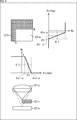
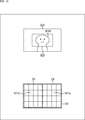
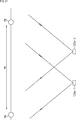
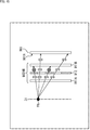
- the object plane 31 of the upper left object in FIG. 1 is composed of the point light source PA to the point light source PC, and the point light source PA to the point light source PC respectively emit a plurality of light rays of light intensity a to light intensity c around It shall be.
- the imaging device 51 includes pixels (hereinafter, referred to as pixels Pa to Pc) having different incident angle directivity at positions Pa to Pc.
- rays of the same light intensity emitted from the same point light source are made incident on the respective pixels of the image sensor 51.
- a light beam of light intensity a emitted from the point light source PA is incident on the pixels Pa to Pc of the imaging device 51, respectively.
- rays emitted from the same point light source are incident at different incident angles for each pixel.
- light rays from the point light source PA are incident on the pixels Pa to Pc at different incident angles.
- the incident angle directivity of the pixels Pa to Pc is different from each other, light rays of the same light intensity emitted from the same point light source are detected with different sensitivities in each pixel. As a result, rays of the same light intensity are detected at different detection signal levels for each pixel. For example, detection signal levels for light rays of light intensity a from the point light source PA have different values in the pixels Pa to Pc.
- the light receiving sensitivity level of each pixel with respect to the light beam from each point light source is determined by multiplying the light intensity of the light beam by a coefficient indicating the light receiving sensitivity (that is, the incident angle directivity) with respect to the incident angle of the light beam.
- the detection signal level of the pixel Pa with respect to the light beam from the point light source PA multiplies the light intensity a of the light beam of the point light source PA by a coefficient indicating the incident angle directivity of the pixel Pa with respect to the incident angle of the light beam to the pixel Pa It is determined by
- the detection signal levels DA, DB, DC of the pixels Pc, Pb, Pa are expressed by the following formulas (1) to (3), respectively.
- DA ⁇ 1 ⁇ a + ⁇ 1 ⁇ b + ⁇ 1 ⁇ c ...
- DB ⁇ 2 ⁇ a + ⁇ 2 ⁇ b + ⁇ 2 ⁇ c ...
- DC ⁇ 3 ⁇ a + ⁇ 3 ⁇ b + ⁇ 3 ⁇ c ...
- the coefficient ⁇ 1 is a coefficient indicating the incident angle directivity of the pixel Pc with respect to the incident angle of the ray from the point light source PA to the pixel Pc, and is set according to the incident angle. Further, ⁇ 1 ⁇ a indicates the detection signal level of the pixel Pc with respect to the light beam from the point light source PA.
- the coefficient ⁇ 1 is a coefficient indicating the incident angle directivity of the pixel Pc with respect to the incident angle of a ray from the point light source PB to the pixel Pc, and is set according to the incident angle. Further, ⁇ 1 ⁇ b represents the detection signal level of the pixel Pc with respect to the ray from the point light source PB.
- the coefficient ⁇ 1 is a coefficient indicating the incident angle directivity of the pixel Pc with respect to the incident angle of the light beam from the point light source PC to the pixel Pc, and is set according to the incident angle. Further, ⁇ 1 ⁇ c indicates the detection signal level of the pixel Pc with respect to the ray from the point light source PC.
- the detection signal level DA of the pixel Pa includes the light intensities a, b and c of the light rays from the point light sources PA, PB and PC at the pixel Pc, and the incident angle directivity according to the respective incident angles. It is obtained by product-sum with coefficients ⁇ 1, ⁇ 1, and ⁇ 1.
- the detection signal level DB of the pixel Pb is, as shown in equation (2), the respective light intensities a, b and c of the light rays from the point light sources PA, PB and PC in the pixel Pb It is obtained by the product-sum with the coefficients ⁇ 2, ⁇ 2, and ⁇ 2 indicating the incident angle directivity according to the angle.
- the detection signal level DC of the pixel Pc is, as shown in the equation (3), the respective light intensities a, b and c of the light rays from the point light sources PA, PB and PC at the pixel Pa and the respective incident angles It is determined by product-sum with the coefficients ⁇ 2, ⁇ 2 and ⁇ 2 indicating the incident angle directivity according to
- the detection signal levels DA, DB, DC of the pixels Pa, Pb, Pc are light of the light beams emitted from the point light sources PA, PB, PC as shown in the equations (1) to (3).
- the strengths a, b and c are mixed. Therefore, as shown in the upper right of FIG. 1, the detection signal level in the imaging device 51 is different from the light intensity of each point light source on the object plane 31. Therefore, the image obtained by the imaging device 51 is different from that on which the image of the object plane 31 is formed.
- a set of coefficients for example, coefficients ⁇ 1, ⁇ 1, ⁇ 1 for each of the equations constituting the simultaneous equations is referred to as a coefficient set.
- a set of a plurality of coefficient sets corresponding to a plurality of equations included in the simultaneous equations for example, coefficient set ⁇ 1, ⁇ 1, ⁇ 1, coefficient set ⁇ 2, ⁇ 2, ⁇ 2, coefficient set ⁇ 3, ⁇ 3, ⁇ 3) Is called a coefficient set group.
- Patent Document 1 Non-Patent Document 1
- Patent Document etc. It is possible to realize an imaging device in which the element 51 is an essential component.
- the imaging lens, the pinhole, and the optical filter described in the patent document and the like do not become an essential component, the height of the imaging device can be reduced, that is, the thickness in the incident direction of light in the configuration realizing the imaging function. It becomes possible to make it thinner.
- the essential configuration is only the imaging device 51, it is possible to improve the degree of freedom in design.
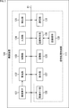
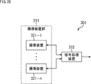
- FIG. 2 is a block diagram showing a configuration example of an imaging device 101 which is a basic imaging device to which the technology of the present disclosure is applied.
- the imaging device 101 includes an imaging element 121, a restoration unit 122, a control unit 123, an input unit 124, a detection unit 125, an association unit 126, a display unit 127, a storage unit 128, a recording and reproduction unit 129, a recording medium 130, and a communication unit. 131 is provided. Further, signal processing and imaging are performed by the restoration unit 122, the control unit 123, the input unit 124, the detection unit 125, the association unit 126, the display unit 127, the storage unit 128, the recording and reproducing unit 129, the recording medium 130, and the communication unit 131.
- a signal processing control unit 111 that controls the device 101 is configured. Note that the imaging device 101 does not include an imaging lens (imaging lens free).
- the imaging device 121, the restoration unit 122, the control unit 123, the input unit 124, the detection unit 125, the association unit 126, the display unit 127, the storage unit 128, the recording and reproduction unit 129, and the communication unit 131 are connected via the bus B1. Are connected to each other, and transmit and receive data via the bus B1.
- the description of the bus B1 in the case where each unit of the imaging apparatus 101 transmits and receives data via the bus B1 is omitted.
- the input unit 124 supplies data to the control unit 123 via the bus B1
- the input unit 124 supplies data to the control unit 123.
- the image pickup device 121 corresponds to the image pickup device 51 described with reference to FIG. 1 and includes a pixel having incident angle directivity, and an image formed of a detection signal indicating a detection signal level corresponding to the amount of incident light. Are output to the restoration unit 122 or the bus B1.
- the imaging device 121 may have the same basic structure as that of a general imaging device such as a complementary metal oxide semiconductor (CMOS) image sensor.
- CMOS complementary metal oxide semiconductor
- the imaging device 121 has a configuration in which the incident angle directivity is given, as will be described later with reference to FIGS. ing.
- the image sensor 121 varies (changes) the light reception sensitivity in accordance with the incident angle of incident light for each pixel, and has incident angle directivity with respect to the incident angle of incident light in pixel units.
- the image output from the imaging element 121 is an image constituted by a detection signal in which the image of the subject is not formed as shown in the upper right of FIG. 1 described above, the subject can be visually recognized. Can not. That is, although the detection image which consists of a detection signal which image sensor 121 outputs is a set of pixel signals, it is an image which can not recognize a subject even if a user looks at a subject (it can not see a subject).
- an image composed of a detection signal on which the image of the subject is not formed, that is, an image captured by the imaging element 121 is referred to as a detected image.
- the imaging device 121 may not be configured as a pixel array, and may be configured as, for example, a line sensor.
- the incident angle directivity does not necessarily have to be all different for each pixel, and the incident angle directivity may include the same pixels.
- the restoration unit 122 corresponds to the subject distance corresponding to the distance from the imaging device 51 to the subject plane 31 (the subject plane corresponding to the restored image) in FIG. 1, for example, and the coefficients ⁇ 1 to ⁇ 3, ⁇ 1 to ⁇ 3, ⁇ 1 described above.
- the coefficient set group corresponding to ⁇ 3 is acquired from the storage unit 128.
- the restoration unit 122 uses the detection signal level of each pixel of the detection image output from the imaging device 121 and the acquired coefficient set group to be represented by the above-described Equations (1) to (3). Make simultaneous equations. Then, the reconstruction unit 122 solves the created simultaneous equations to obtain the pixel values of the respective pixels constituting the image on which the image of the subject shown in the lower right of FIG. 1 is formed.
- an image from which the user can visually recognize and recognize the subject (and can visually recognize the subject) is restored from the detected image.
- an image restored from the detected image will be referred to as a restored image.
- the restored image is not an image that can identify the subject as a normal image, but also in this case the restored image It is called.
- a restored image which is an image in a state in which an image of a subject is formed, and an image before color separation such as demosaicing processing or synchronization processing is referred to as a RAW image
- the detected image is distinguished as an image according to the array of color filters but not a RAW image.
- the number of pixels of the imaging device 121 and the number of pixels of the pixels forming the restored image do not necessarily have to be the same.
- the restoration unit 122 performs demosaicing processing, ⁇ correction, white balance adjustment, conversion processing to a predetermined compression format, and the like on the restored image as necessary. Then, the restoration unit 122 outputs the restored image to the bus B1.
- the control unit 123 includes, for example, various processors, and controls each unit of the imaging apparatus 101.
- the input unit 124 includes an input device (for example, a key, a switch, a button, a dial, a touch panel, a remote controller, and the like) for performing an operation of the imaging apparatus 101, an input of data used for processing, and the like.
- the input unit 124 outputs an operation signal, input data, and the like to the bus B1.
- the detection unit 125 includes the imaging device 101 and various sensors used to detect the state of the subject and the like.
- the detection unit 125 may be an acceleration sensor or a gyro sensor that detects the posture or movement of the imaging device 101, a position detection sensor (for example, a GNSS (Global Navigation Satellite System) receiver) that detects the position of the imaging device 101, an object A distance measuring sensor or the like for detecting a distance is provided.
- the detection unit 125 outputs a signal indicating the detection result to the bus B1.
- the associating unit 126 associates the detection image obtained by the imaging device 121 with the metadata corresponding to the detection image.
- the metadata includes, for example, a coefficient set group for restoring a restored image using a target detection image, an object distance, and the like.
- the method of associating the detection image with the metadata is not particularly limited as long as the correspondence between the detection image and the metadata can be specified. For example, metadata is added to image data including a detected image, the same ID is added to a detected image and metadata, or the detected image and metadata are recorded on the same recording medium 130. Metadata is associated.
- the display unit 127 is, for example, a display, and displays various types of information (for example, a restored image and the like). Note that the display unit 127 can also be provided with an audio output unit such as a speaker to output audio.
- the storage unit 128 includes one or more storage devices such as a read only memory (ROM), a random access memory (RAM), and a flash memory, and stores, for example, programs and data used for processing of the imaging device 101.
- the storage unit 128 stores coefficient set groups corresponding to the above-described coefficients ⁇ 1 to ⁇ 3, ⁇ 1 to ⁇ 3, and ⁇ 1 to ⁇ 3 in association with various object distances. More specifically, for example, the storage unit 128 stores, for each subject plane 31 at each subject distance, a coefficient set group including a coefficient for each pixel 121a of the image sensor 121 for each point light source set on the subject plane 31. doing.
- the recording and reproduction unit 129 performs recording of data on the recording medium 130 and reproduction (reading) of data recorded on the recording medium 130.
- the recording / reproducing unit 129 records the restored image on the recording medium 130 or reads the restored image from the recording medium 130.
- the recording / reproducing unit 129 records the detection image and the corresponding metadata on the recording medium 130 or reads out from the recording medium 130.
- the recording medium 130 is made of, for example, any of a hard disk drive (HDD), a solid state drive (SSD), a magnetic disk, an optical disk, a magneto-optical disk, a semiconductor memory, or a combination thereof.
- HDD hard disk drive
- SSD solid state drive
- magnetic disk magnetic disk
- optical disk magnetic disk
- magneto-optical disk magnetic disk
- semiconductor memory or a combination thereof.
- the communication unit 131 communicates with another device (for example, another imaging device, a signal processing device, and the like) by a predetermined communication method.
- the communication method of the communication unit 131 may be wired or wireless. Further, the communication unit 131 can also correspond to a plurality of communication methods.
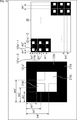
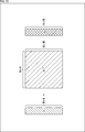
- FIG. 3 shows a front view of a part of the pixel array portion of the imaging element 121.
- FIG. 3 shows an example in which the number of pixels in the pixel array portion is 6 vertical pixels ⁇ 6 horizontal pixels, the number of pixels in the pixel array portion is not limited to this.
- a light shielding film 121b which is one of the modulation elements, is provided for each pixel 121a so as to cover a part of the light receiving area (light receiving surface) of the photodiode. Incident incident light is optically modulated according to the incident angle. Then, for example, by providing the light shielding film 121b in a different range for each pixel 121a, the light receiving sensitivity with respect to the incident angle of incident light differs for each pixel 121a, and each pixel 121a has different incident angle directivity .
- the light shielding film 121b-1 and the light shielding film 121b-2 provided in the pixel 121a-1 and the pixel 121a-2 have different ranges for shielding the light receiving region of the photodiode (a light shielding region (position), And at least one of the shaded areas). That is, in the pixel 121a-1, the light shielding film 121b-1 is provided so as to shield a part of the left side of the light receiving region of the photodiode by a predetermined width. On the other hand, in the pixel 121a-2, a light shielding film 121b-2 is provided so as to shield a part of the right side of the light receiving region by a predetermined width.
- the width at which the light shielding film 121b-1 shields the light receiving area of the photodiode may be different from or the same as the width at which the light shielding film 121b-2 shields the light receiving area of the photodiode. .
- the light shielding films 121b are randomly arranged in the pixel array so as to shield a different range of the light receiving area for each pixel.
- the amount of light that can be received by the photodiode decreases as the rate at which the light shielding film 121b obscures the light receiving area of each pixel increases. Therefore, it is desirable that the area of the light shielding film 121b be such an area that a desired light quantity can be secured, and for example, a restriction of up to about 3/4 of the light receiving area may be added. By doing this, it is possible to secure a light amount of a desired amount or more. However, it is possible to receive a minimum amount of light if each pixel is provided with an unshielded range having a width corresponding to the wavelength of light to be received. That is, for example, in the case of the B pixel (blue pixel), the wavelength is about 500 nm, but it is possible to receive the minimum light amount unless the light is blocked beyond the width corresponding to this wavelength.
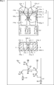
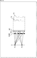
- the upper part of FIG. 4 is a side cross-sectional view of the first configuration example of the imaging device 121
- the middle part of FIG. 4 is a top view of the first configuration example of the imaging device 121.
- the side cross-sectional view of the upper stage of FIG. 4 is an AB cross section in the middle stage of FIG. 4.
- the lower part of FIG. 4 is a circuit configuration example of the imaging element 121.
- the adjacent pixels 121a-1 and 121a-2 are so-called back side illumination type in which the wiring layer Z12 is provided in the lowermost layer in the drawing and the photoelectric conversion layer Z11 is provided thereon.
- the description of the numbers at the end of the reference numerals is omitted and simply referred to as the pixel 121a.
- the numbers at the end of the reference numerals may be omitted in the same manner for the other configurations.
- FIG. 4 shows only the side view and the top view of two pixels constituting the pixel array of the image sensor 121, and needless to say, although more pixels 121a are arranged, Is omitted.
- the pixels 121a-1 and 121a-2 respectively include photodiodes 121e-1 and 121e-2 in the photoelectric conversion layer Z11.
- on-chip lenses 121c-1 and 121c-2 and color filters 121d-1 and 121d-2 are stacked on the photodiodes 121e-1 and 121e-2, respectively.
- the on-chip lenses 121c-1 and 121c-2 condense incident light on the photodiodes 121e-1 and 121e-2.
- the color filters 121d-1 and 121d-2 are optical filters that transmit light of a specific wavelength, such as red, green, blue, infrared, and white. In the case of white, the color filters 121d-1 and 121d-2 may or may not be transparent filters.
- Light shielding films 121g-1 to 121g-3 are formed at the boundaries between the pixels in the photoelectric conversion layer Z11 of the pixels 121a-1 and 121a-2, and for example, as shown in FIG. L is incident on an adjacent pixel to suppress the occurrence of crosstalk.
- the light shielding films 121b-1 and 121b-2 shield a part of the light receiving surface S as viewed from the top.
- different ranges are shielded by the light shielding films 121b-1 and 121b-2, respectively, whereby different incident angles are obtained.
- the directivity is set independently for each pixel.
- the light shielding range does not have to be different for all the pixels 121 a of the imaging device 121, and some pixels 121 a may have the same light shielding region.
- the light shielding film 121b-1 and the light shielding film 121g-1 are connected to each other, and are L-shaped when viewed from the side.
- the light shielding film 121b-2 and the light shielding film 121g-2 are connected to each other, and are configured in an L shape when viewed from the side.
- the light shielding film 121b-1, the light shielding film 121b-2, and the light shielding films 121g-1 to 121g-3 are made of metal, and for example, tungsten (W), aluminum (Al), or Al and copper Composed of an alloy with (Cu).
- the light shielding film 121b-1, the light shielding film 121b-2, and the light shielding films 121g-1 to 121g-3 are simultaneously formed of the same metal as the wiring in the same process as the wiring in the semiconductor process. It may be done.
- the film thicknesses of the light shielding film 121b-1, the light shielding film 121b-2, and the light shielding films 121g-1 to 121g-3 may not be the same depending on the position.
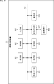
- the pixel 121 a includes a photodiode 161 (corresponding to the photodiode 121 e), a transfer transistor 162, an FD (Floating Diffusion: floating diffusion) portion 163, a selection transistor 164, and an amplification transistor 165. And a reset transistor 166, and is connected to the current source 168 via the vertical signal line 167.
- the anode electrode of the photodiode 161 is grounded, and the cathode electrode is connected to the gate electrode of the amplification transistor 165 via the transfer transistor 162.
- the transfer transistor 162 is driven according to the transfer signal TG. For example, when the transfer signal TG supplied to the gate electrode of the transfer transistor 162 becomes high level, the transfer transistor 162 is turned on. Thereby, the charge accumulated in the photodiode 161 is transferred to the FD unit 163 via the transfer transistor 162.
- the amplification transistor 165 is an input portion of a source follower which is a readout circuit for reading out a signal obtained by photoelectric conversion in the photodiode 161, and a pixel signal of a level corresponding to the charge stored in the FD portion 163 is a vertical signal line 167. Output to That is, the amplification transistor 165 has a drain terminal connected to the power supply VDD and a source terminal connected to the vertical signal line 167 via the selection transistor 164, thereby connecting the current source 168 connected to one end of the vertical signal line 167. Configure a source follower.
- the FD unit 163 is a floating diffusion region having a charge capacity C1 provided between the transfer transistor 162 and the amplification transistor 165, and temporarily accumulates the charge transferred from the photodiode 161 via the transfer transistor 162.
- the FD unit 163 is a charge detection unit that converts a charge into a voltage, and the charge stored in the FD unit 163 is converted into a voltage by the amplification transistor 165.
- the selection transistor 164 is driven according to the selection signal SEL, and is turned on when the selection signal SEL supplied to the gate electrode becomes high level, and connects the amplification transistor 165 and the vertical signal line 167.
- the reset transistor 166 is driven according to the reset signal RST. For example, the reset transistor 166 is turned on when the reset signal RST supplied to the gate electrode becomes high level, discharges the charge stored in the FD unit 163 to the power supply VDD, and resets the FD unit 163.
- the pixel circuit shown in the lower part of FIG. 4 operates as follows.
- the reset transistor 166 and the transfer transistor 162 are turned on, the charge stored in the FD unit 163 is discharged to the power supply VDD, and the FD unit 163 is reset.
- the reset transistor 166 and the transfer transistor 162 are turned off, and during the exposure period, the photodiode 161 accumulates a charge according to the amount of incident light.
- the reset transistor 166 is turned on and the FD section 163 is reset, and then the reset transistor 166 is turned off.
- the FD unit 163 is set to the reference potential.
- the potential of the FD section 163 in a reset state is output from the amplification transistor 165 as a reference potential.
- the transfer transistor 162 is turned on, and the charge accumulated in the photodiode 161 is transferred to the FD portion 163.
- the potential of the FD section 163 to which the charge of the photodiode is transferred is output from the amplification transistor 165 as a signal potential.
- a signal obtained by subtracting the reference potential from the signal potential by CDS is output as a detection signal (pixel signal) of the pixel 121a.
- the value (output pixel value) of the detection signal is modulated according to the incident angle of incident light from the subject, and the characteristic (directivity) differs depending on the incident angle (having incident angle directivity).
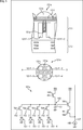
- FIG. 5 is a diagram showing a second configuration example of the imaging device 121.
- the upper side of FIG. 5 shows a side cross-sectional view of the pixel 121a of the imaging device 121 which is the second configuration example, and the middle stage of FIG. 5 shows a top view of the imaging device 121.
- the side cross-sectional view of the upper stage of FIG. Furthermore, the lower part of FIG. 5 is a circuit configuration example of the imaging element 121.
- the imaging device 121 of FIG. 5 In the imaging device 121 of FIG. 5, four photodiodes 121f-1 to 121f-4 are formed in one pixel 121a, and a light shielding film 121g is formed in a region separating the photodiodes 121f-1 to 121f-4.
- the configuration is different from that of the imaging device 121 of FIG. That is, in the imaging element 121 of FIG. 5, the light shielding film 121 g is formed in a “+” shape when viewed from the upper surface.
- symbol same as FIG. 4 is attached
- the photodiodes 121 f-1 to 121 f-4 are separated by the light shielding film 121 g, so that electrical and optical crosstalk between the photodiodes 121 f-1 to 121 f-4 occurs. It is prevented. That is, the light shielding film 121g of FIG. 5 is for preventing crosstalk similarly to the light shielding film 121g of the imaging device 121 of FIG. 4, and is not for providing incident angle directivity.
- one FD unit 163 is shared by the four photodiodes 121f-1 to 121f-4.
- the lower part of FIG. 5 shows an example of a circuit configuration in which one FD portion 163 is shared by four photodiodes 121f-1 to 121f-4. In the lower part of FIG. 5, the description of the same configuration as the lower part of FIG. 4 is omitted.
- the lower part of FIG. 5 differs from the circuit configuration of the lower part of FIG. 4 in that photodiodes 161-1 to 161- are used instead of the photodiode 161 (corresponding to the photodiode 121e in the upper part of FIG. 4) and the transfer transistor 162. 4 (corresponding to the photodiodes 121f-1 to 121f-4 in the upper part of FIG. 5) and the transfer transistors 162-1 to 162-4 and share the FD section 163.
- the charge accumulated in the photodiodes 121f-1 to 121f-4 has a predetermined capacitance provided at the connection portion between the photodiodes 121f-1 to 121f-4 and the gate electrode of the amplification transistor 165. It is transferred to the common FD unit 163. Then, a signal corresponding to the level of the charge held in the FD unit 163 is read as a detection signal (pixel signal) (however, the CDS processing is performed as described above).
- the charges accumulated in the photodiodes 121f-1 to 121f-4 can be selectively contributed to the output of the pixel 121a, that is, the detection signal in various combinations. That is, the photodiodes 121f-1 to 121f-4 are configured to be able to read out the charge independently, and the photodiodes 121f-1 to 121f-4 (the photodiodes 121f-1 to 121f-4 output Different incident angle directivity can be obtained.
- the incident angle directivity in the left-right direction can be obtained.
- the incident angle directivity in the vertical direction by transferring the electric charges of the photodiode 121f-1 and the photodiode 121f-3 to the FD portion 163 and adding the signals obtained by reading out each, the incident angle directivity in the left-right direction can be obtained.
- the incident angle directivity in the vertical direction by transferring the electric charges of the photodiode 121f-1 and the photodiode 121f-2 to the FD portion 163 and adding the signals obtained by reading the respective, it is possible to obtain the incident angle directivity in the vertical direction.
- a signal obtained based on the charges selectively read out independently from the four photodiodes 121f-1 to 121f-4 is a detection signal corresponding to one pixel constituting the detection image.
- the contribution of (the charge of) each photodiode 121f to the detection signal is not limited to, for example, whether or not the charge (the detected value) of each photodiode 121f is transferred to the FD unit 163, but also using an electronic shutter function. This can also be realized by resetting the charge accumulated in the photodiode 121 f before transfer to the FD unit 163. For example, if the charge of the photodiode 121f is reset immediately before transfer to the FD portion 163, the photodiode 121f does not contribute to the detection signal at all. On the other hand, by giving time to the charge of the photodiode 121f between the reset and the transfer of the charge to the FD portion 163, the photodiode 121f partially contributes to the detection signal.
- the combination of the four photodiodes 121 f-1 to 121 f-4 used for the detection signal is changed to have different incident angle directivity for each pixel.
- the detection signal output from each pixel 121a of the image sensor 121 in FIG. 5 has a value (output pixel value) modulated according to the incident angle of the incident light from the subject, and the characteristic (directivity) according to the incident angle Are different (having incident angle directivity).
- the pixel output unit includes at least one or more photodiodes, and generally, each pixel 121a of the imaging device 121 corresponds to one pixel output unit.
- one pixel output unit includes one photodiode 121 e.
- one pixel 121e constitutes one pixel output unit.
- the incident angle directivity of each pixel output unit can be made different.
- incident light to each pixel 121a is optically modulated using the light shielding film 121b, and as a result, the incident angle is directed by the signal output from the photodiode 121e of each pixel 121a.
- a detection signal for one pixel of the detected image reflecting the polarity is obtained. That is, the image pickup device 121 of FIG. 4 includes a plurality of pixel output units for receiving incident light from an object incident without any of the imaging lens and the pinhole, and each pixel output unit includes one photodiode 121e.
- the characteristic (incident angle directivity) with respect to the incident angle of incident light from the subject is set for each pixel output unit.
- one pixel output unit includes four photodiodes 121e. Become. In other words, one pixel output unit is configured by the four photodiodes 121 f. On the other hand, individual pixel output units are not configured by each photodiode 121e alone.
- the incident angle directivity for each pixel output unit is different. It becomes a thing. That is, in the imaging device 121 of FIG. 5, the range not contributing to the output (detection signal) among the four photodiodes 121f-1 to 121f-4 functions in the same manner as the light-shielded region. Then, by combining the signals output from the photodiodes 121f-1 to 121f-4, a detection signal for one pixel of the detection image reflecting the incident angle directivity is obtained. That is, the imaging device 121 of FIG.
- each pixel output unit includes a plurality of photodiodes (for example, Characteristics (incident angle directivity) of each pixel output unit with respect to the incident angle of incident light from the subject by providing the photodiodes 121f-1 to 121f-4) and varying (the degree of) the photodiodes contributing to the output Are different from each other.
- photodiodes for example, Characteristics (incident angle directivity) of each pixel output unit with respect to the incident angle of incident light from the subject by providing the photodiodes 121f-1 to 121f-4) and varying (the degree of) the photodiodes contributing to the output Are different from each other.
- incident light is incident on all the photodiodes 121f-1 to 121f-4 without being optically modulated, so that the detection signal is a signal obtained by optical modulation. Absent. Further, hereinafter, the photodiode 121 f not contributing to the detection signal is also referred to as a photodiode 121 f not contributing to a pixel output unit or an output.
- the light receiving surface of the pixel output unit (pixel 121a) is equally divided into four, and photodiodes 121f having the same size as the light receiving surface are arranged in each region, that is, four photodiodes, etc.
- the division number and division position of the photodiode can be set arbitrarily.
- the photodiodes do not necessarily have to be equally divided, and the division positions of the photodiodes may be different for each pixel output unit.
- the incident angle directivity differs between the pixel output units.
- by setting the number of divisions to be different between pixel output units it is possible to more freely set the incident angle directivity.
- both the division number and the division position may be made different between pixel output units.
- each of the image sensor 121 of FIG. 4 and the image sensor 121 of FIG. 5 has a configuration in which each pixel output unit can independently set the incident angle directivity.
- each pixel output unit of an image sensor does not have the composition which can set up incidence angle directivity independently.
- the incident angle directivity of each pixel output unit is set by the light shielding film 121 b at the time of manufacture.
- the image sensor 121 of FIG. 4 the image sensor 121 of FIG.
- the division number and division position of the photodiode of each pixel output unit are set at the time of manufacture, but the incident angle directivity of each pixel output unit (combination of photodiodes contributing to output) Can be set at the time of use (for example, at the time of imaging).
- the imaging device 121 of FIG. 4 and the imaging device 121 of FIG. 5 it is not necessary to have a configuration in which all the pixel output units have incident angle directivity.
- each pixel of the imaging device corresponds to one pixel output unit, but as described later, there may be a case where one pixel output unit is formed by a plurality of pixels. . The following description will be made assuming that each pixel of the imaging device corresponds to one pixel output unit unless otherwise noted.
- the incident angle directivity of each pixel of the imaging element 121 is generated, for example, according to the principle shown in FIG.
- the upper left part and the upper right part of FIG. 6 are diagrams for explaining the generation principle of the incident angle directivity in the imaging element 121 of FIG. 4, and the lower left part and the lower right part of FIG. 6 are for the imaging element 121 of FIG. It is a figure explaining the generation
- Each of the upper left and upper right pixels in FIG. 6 includes one photodiode 121 e.
- the lower left and lower right pixels in FIG. 6 each include two photodiodes 121 f.
- an example in which one pixel includes two photodiodes 121 f is shown here, this is for convenience of explanation, and the number of photodiodes 121 f provided in one pixel may be another number. .
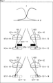
- a light shielding film 121b-11 is formed to shield the right half of the light receiving surface of the photodiode 121e-11. Further, in the pixel at the upper right portion of FIG. 6, a light shielding film 121b-12 is formed so as to shield the left half of the light receiving surface of the photodiode 121e-12. Note that the alternate long and short dash line in the drawing is an auxiliary line which passes through the horizontal center of the light receiving surface of the photodiode 121e and is perpendicular to the light receiving surface.
- incident light from the upper right direction forming the incident angle ⁇ 1 with respect to the alternate long and short dash line in the drawing is left unshielded by the light shielding film 121b-11 of the photodiode 121e-11. It is easy to receive light by the half range.
- incident light from the upper left direction forming the incident angle ⁇ 2 with respect to the alternate long and short dash line in the figure is hard to be received by the left half range not blocked by the light shielding film 121b-11 of the photodiode 121e-11. . Therefore, the pixel in the upper left part of FIG. 6 has high incidence sensitivity with respect to incident light from the upper right in the figure and low sensitivity to incident light from the upper left. .
- incident light from the upper right direction forming the incident angle ⁇ 1 is received by the left half range shielded by the light shielding film 121b-12 of the photodiode 121e-12. Hateful.
- incident light from the upper left direction forming the incident angle ⁇ 2 is likely to be received by the right half range which is not blocked by the light shielding film 121b-12 of the photodiode 121e-12. Therefore, the pixel in the upper right part of FIG. 6 has low incident sensitivity to incident light from the upper right in the figure and high incident sensitivity to incident light from the upper left. .
- photodiodes 121f-11 and 121f-12 are provided on the left and right in the drawing, and a light shielding film 121b is provided by reading out one of the detection signals. It is set as the structure which has incident angle directivity.
- incident angle directivity similar to that of the upper left part in FIG. You can get it. That is, incident light from the upper right direction forming the incident angle ⁇ 1 with respect to the alternate long and short dash line in the figure is incident on the photodiode 121f-11 and a signal corresponding to the amount of light received is read out from the photodiode 121f-11. It contributes to the detection signal output from the pixel.
- incident light from the upper left direction forming the incident angle ⁇ 2 with respect to the alternate long and short dash line in the figure is incident on the photodiode 121f-12 but is not read out from the photodiode 121f-12. It does not contribute to the output detection signal.
- incident light from the upper left direction forming the incident angle ⁇ 2 is incident on the photodiode 121f-14, and a signal corresponding to the amount of light received is read out from the photodiode 121f-14, so that it is output from this pixel Contribute to the detection signal.
- the upper graph in FIG. 7 shows the incident angle directivity of the middle and lower pixels in FIG.
- the horizontal axis represents the incident angle ⁇
- the vertical axis represents the detection signal level.
- the incident angle ⁇ is 0 degrees when the direction of incident light coincides with the alternate long and short dash line in the middle left of FIG. 7, and the middle left incident angle ⁇ 21 in FIG. 7 is a positive direction.
- the right incident angle ⁇ 22 side is a negative direction. Therefore, with respect to the on-chip lens 121c, the incident angle of the incident light entering from the upper right is larger than the incident angle of the incident light entering from the upper left. That is, the incident angle ⁇ becomes larger as the traveling direction of the incident light leans to the left (larger in the positive direction) and smaller as it leans to the right (larger in the negative direction).
- the pixels in the middle left part of FIG. 7 are the on-chip lens 121 c-11 for condensing incident light and the color filters 121 d-11 for transmitting light of a predetermined wavelength to the pixels in the upper left part of FIG. Is added. That is, in this pixel, the on-chip lens 121c-11, the color filter 121d-11, the light shielding film 121b-11, and the photodiode 121e-11 are laminated in order from the incident direction of the upper light in the drawing.
- the pixel at the middle right of FIG. 7, the pixel at the lower left of FIG. 7, and the pixel at the lower right of FIG. 7 are respectively the pixel at the upper right of FIG. 6 and the lower left of FIG.
- the on-chip lens 121 c-11 and the color filter 121 d-11 or the on-chip lens 121 c-12 and the color filter 121 d-12 are added to the pixel of FIG.
- the detection signal level (light receiving sensitivity) of the photodiode 121e-11 changes according to the incident angle ⁇ of incident light. That is, the larger the incident angle ⁇ which is the angle formed by the incident light with respect to the alternate long and short dash line in the figure (the larger the incident angle ⁇ in the positive direction (the more inclined in the right direction in the figure)) When the light is collected in the range in which 11 is not provided, the detection signal level of the photodiode 121e-11 is increased.
- the smaller the incident angle ⁇ of the incident light the larger the incident angle ⁇ in the negative direction (the more inclined in the left direction in the figure)
- the light is collected in the range in which the light shielding film 121b-11 is provided.
- the detection signal level of the photodiode 121e-11 decreases.
- the detection signal level (light receiving sensitivity) of the photodiode 121e-12 changes according to the incident angle ⁇ of incident light.
- the incident angle ⁇ of the incident light is larger (the incident angle ⁇ is larger in the positive direction)
- the light is condensed in the range in which the light shielding film 121b-12 is provided, thereby the photodiode 121e-12.
- the detection signal level increases.
- the waveforms of the solid line and the dotted line shown in the upper part of FIG. 7 can be changed according to the range of the light shielding film 121 b. Therefore, it is possible to give different incident angle directivity to each other in pixel units by the range of the light shielding film 121b.
- the incident angle directivity is a characteristic of the light receiving sensitivity of each pixel according to the incident angle ⁇ , but this is a characteristic of the light blocking value according to the incident angle ⁇ in the middle pixel of FIG. It can be said that That is, although the light shielding film 121 b blocks incident light in a specific direction at a high level, incident light from other directions can not be blocked sufficiently.
- the change of the light shieldable level produces different detection signal levels according to the incident angle ⁇ as shown in the upper part of FIG.
- the direction in which light can be blocked at the highest level in each pixel is defined as the light blocking direction of each pixel, having different incident angle directivity in pixel units means, in other words, light blocking mutually different in pixel units It means that it has a direction.
- the middle left pixel in FIG. 7 It is possible to obtain incident angle directivity similar to that of the pixels of a part. That is, when the incident angle ⁇ of the incident light increases (when the incident angle ⁇ increases in the positive direction), the light is collected in the range of the photodiode 121f-11 from which the signal is read, and the detection signal level is large. Become. Conversely, the smaller the incident angle ⁇ of the incident light (the larger the incident angle ⁇ in the negative direction), the more light is collected in the range of the photodiode 121 f-12 from which the signal is not read out, and thus the detection signal level Becomes smaller.
- the signal of only the photodiode 121 f-14 in the right in FIG. An incident angle directivity similar to that of the pixel in the middle right part of can be obtained. That is, when the incident angle ⁇ of incident light increases (when the incident angle ⁇ increases in the positive direction), light is collected in the range of the photodiode 121 f-13 that does not contribute to the output (detection signal). The level of the unit detection signal decreases.
- the smaller the incident angle ⁇ of the incident light the larger the incident angle ⁇ in the negative direction
- the more light is collected in the range of the photodiode 121f-14 that contributes to the output (detection signal)
- the level of the detection signal in units of pixels is increased.
- each photodiode has directivity with respect to the incident angle of incident light
- the on-chip lens 121c is an essential component of each pixel in order to generate incident angle directivity in pixel units.
- the incident angle directivity it is desirable that the randomness be high in pixel units.
- the above-described equations (1) to (3) or equations (4) to (6) described later may be the same as each other.
- the number of equations is insufficient for the unknowns that are solutions of simultaneous equations, which may make it impossible to obtain the pixel values that make up the restored image.
- the light shielding film 121b that shields the entire light receiving surface of the pixel 121a in the vertical direction and shields the light receiving surface with a predetermined width in the horizontal direction It is called a band type light shielding film 121b.
- a light shielding film 121b that shields the entire light receiving surface of the pixel 121a in the horizontal direction and shields the light receiving surface at a predetermined height in the vertical direction is referred to as a vertical band type light shielding film 121b.
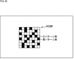
- an L-shaped light shielding film 121 b is formed for each pixel of the Bayer arrangement. It may be provided.
- the black range represents the light shielding film 121b, and the same applies to the following drawings unless otherwise noted.
- the pixels 121a-21 and 121a-24 of G (green) pixels, the pixels 121a-22 of R (red) pixels, and the pixels 121a-23 of B (blue) pixels, which are in the Bayer array, are provided.
- L-shaped light shielding films 121b-21 to 121b-24 are provided for each of them.
- each pixel 121a has incident angle directivity as shown in the right part of FIG. That is, in the right part of FIG. 8, the distribution of the light receiving sensitivity of each pixel 121a is shown, the horizontal axis represents the incident angle ⁇ x in the horizontal direction (x direction) of the incident light, and the vertical axis is the vertical of the incident light
- the incident angle ⁇ y in the direction (y direction) is represented.
- the light receiving sensitivity in the range C4 is higher than the outside of the range C4
- the light receiving sensitivity in the range C3 is higher than the outside of the range C3
- the light receiving sensitivity in the range C2 is higher than the outside of the range C2.
- the light reception sensitivity in the range C1 is higher than the outside of the range C1.
- the detection signal level for the incident light in which the incident angle ⁇ x in the horizontal direction (x direction) and the incident angle ⁇ y in the vertical direction (y direction) fall within the range C1 is the highest. Then, the detection signal level decreases in the order of incident light in which the incident angle ⁇ x and the incident angle ⁇ y fall within the range C2, within the range C3, within the range C4, and outside the range C4.
- the intensity distribution of the light receiving sensitivity shown in the right part of FIG. 8 is determined by the range shielded by the light shielding film 121b in each pixel 121a regardless of the Bayer arrangement.
- the light shielding film 121b is generically referred to as an L-shaped light shielding film 121b.
- the light shielding range in the horizontal direction of the light shielding film 121b is from the left end of the pixel 121a to the position A, and the light shielding range in the vertical direction is from the upper end of the pixel 121a
- the range is up to B.
- the weights Wx and Wy change as in the graph of FIG. 9 when ideal conditions are satisfied.
- the incident angle directivity of each pixel 121a that is, the coefficient corresponding to the light receiving sensitivity characteristic
- a value obtained by multiplying the weight Wx corresponding to the incident angle ⁇ x of incident light from a certain point light source on the object surface 31 and the weight Wy corresponding to the incident angle ⁇ y is set as the coefficient for the point light source.
- the inclination (1 / 2 ⁇ ) indicating the change of the weight in the range in which the weight Wx in the horizontal direction and the weight Wy in the vertical direction are around 0.5 is obtained by using the on-chip lens 121c having different focal lengths. It can be set.
- the focal length of the on-chip lens 121c matches the surface of the light shielding film 121b
- the focal length of the on-chip lens 121c changes with the curvature of the on-chip lens 121c. Therefore, different incident angle directivity, that is, different light receiving sensitivity characteristics can be obtained by changing the focal length of the on-chip lens 121 c using the on-chip lens 121 c having different curvatures.
- the incident angle directivity of the pixel 121a can be adjusted by the combination of the range in which the photodiode 121e is shielded by the light shielding film 121b and the curvature of the on-chip lens 121c.
- the curvature of the on-chip lens may be the same for all the pixels 121 a of the imaging device 121 or may be different for some of the pixels 121 a.
- each pixel 121a For example, based on the position of each pixel 121a, the shape, position and range of the light shielding film 121b of each pixel 121a, and the curvature of the on-chip lens 121c as an index indicating the incident angle directivity of each pixel 121a of the image sensor 121.
- the characteristics of the weight Wx and the weight Wy as in the graph of FIG. 9 are set for each pixel 121a.
- the incident angle of the light beam from the point light source to the pixel 121a is obtained.
- the coefficient of the pixel 121a with respect to the point light source is determined.
- the coefficients are obtained as described above to obtain the coefficient sets ⁇ 1 and ⁇ 1 of the equations (1) to (3) described above.
- the coefficient set group of the image sensor 121 with respect to the object plane 31 can be obtained, such as ⁇ 1, ⁇ 1, coefficient set ⁇ 2, ⁇ 2, ⁇ 2, coefficient set ⁇ 3, ⁇ 3, ⁇ 3.
- the incident angle of the light beam from each point light source of the subject surface 31 to the imaging device 121 is Because they are different, different coefficient set groups are required for each subject distance.
- each pixel 121 a needs to be set so as to ensure the independence of the above-described simultaneous equations.
- the imaging element 121 does not require an optical block or a pinhole formed of an imaging lens, but as described above, the on-chip lens 121 c is provided.
- the on-chip lens 121c and the imaging lens have different physical actions.
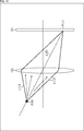
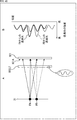
- the imaging lens 152 is designed to condense diffused light incident at different angles from the point light source P101 at the pixel position P111 and form an image of the point light source P101.
- the pixel position P111 is specified by the chief ray L101 passing through the point light source P101 and the center of the imaging lens 152.
- the imaging lens 152 is designed to condense diffused light incident at different angles from the point light source P102 at the pixel position P112 and form an image of the point light source P102.
- the pixel position P112 is specified by the chief ray L102 passing through the point light source P102 and the center of the imaging lens 152.
- the imaging lens 152 forms images of point light sources P101 and P102 having different chief rays at different pixel positions P111 and P112 on the imaging element 151.
- the imaging lens 152 when the point light source P101 is at infinity, a part of the diffused light emitted from the point light source P101 is incident on the imaging lens 152 as parallel light parallel to the chief ray L101.
- parallel light which is a light ray between the light ray L121 and the light ray L122 parallel to the chief ray L101, enters the imaging lens 152.
- the parallel light incident on the imaging lens 152 is condensed at the pixel position P111 on the imaging element 151. That is, the imaging lens 152 is designed to condense parallel light from the point light source P101 existing at infinity into the pixel position P111 and form an image of the point light source P101.
- the imaging lens 152 causes diffused light from a point light source having a chief ray incident angle ⁇ 1 to enter into the pixel (pixel output unit) P1 and has a chief ray incident angle ⁇ 2 different from the chief ray incident angle ⁇ 1. It has a light collecting function of causing diffused light from a light source to be incident on a pixel (pixel output unit) P2 different from the pixel P1. That is, the imaging lens 152 has a light collecting function for causing diffused light from light sources with different incident angles of principal rays to a plurality of pixels (pixel output units) adjacent to each other. However, for example, light from point light sources close to each other or point light sources existing at infinity and substantially close to each other may be incident on the same pixel (pixel output unit).
- the light passing through the on-chip lens 121c is received by the photodiode 121e or the photodiode 121f constituting the corresponding pixel (pixel output unit). It is incident only on the surface.
- the on-chip lens 121 c is provided for each pixel (pixel output unit), and condenses incident light incident thereon to only the corresponding pixel (pixel output unit). That is, the on-chip lens 121c does not have a light collecting function for causing light from different point light sources to be incident on different pixels (pixel output units).
- the incident angle directivity can not be set freely and freely for each pixel.
- DA ⁇ 1 ⁇ a + ⁇ 1 ⁇ b + ⁇ 1 ⁇ c ...
- DB ⁇ 2 ⁇ a + ⁇ 2 ⁇ b + ⁇ 2 ⁇ c ...
- DC ⁇ 3 ⁇ a + ⁇ 3 ⁇ b + ⁇ 3 ⁇ c ...
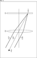
- the object surface 31 ′ at which the object distance to the image pickup element 121 is a distance d 2 larger by d than the distance d 1 is a distance d 2 larger by d than the distance d 1
- the detection signal levels at the pixels Pc, Pb and Pa on the image sensor 121 are the same as the detection signal levels DA, DB and DC as shown in the lower center of FIG. become.
- the coefficient set group consisting of the coefficient sets ⁇ 11, ⁇ 11, ⁇ 11, the coefficient sets ⁇ 12, ⁇ 12, ⁇ 12, the coefficient sets ⁇ 13, ⁇ 13, ⁇ 13 is the coefficient sets ⁇ 1, ⁇ 1, ⁇ 1 and the coefficient sets ⁇ 2, ⁇ 2 for the object surface 31. , ⁇ 2, and coefficient sets ⁇ 3, ⁇ 3, and ⁇ 3 for the object plane 31 ′.
- the object plane can be obtained by solving the simultaneous equations of equations (4) to (6) using preset coefficient set groups ⁇ 11, ⁇ 11, ⁇ 11, ⁇ 12, ⁇ 12, ⁇ 13, ⁇ 13, ⁇ 13.
- the point light source PA ′ of the object surface 31 ′ as shown in the lower right of FIG. 13, in the same manner as in the case of obtaining the light intensities a, b and c of the light from the 31 point light sources PA, PB and PC.
- the light intensities a ', b' and c 'of the rays from PB' and PC ' can be determined. As a result, it is possible to restore the restored image of the subject surface 31 '.
- a coefficient set group for each distance (subject distance) from the imaging element 121 to the subject surface is prepared in advance, and the coefficient set group is switched for each subject distance to perform simultaneous equations.
- the coefficient set group is switched according to the distance to the object surface using the recorded detected image, and the restored image is restored. It is possible to generate a restored image of the object plane.
- the pixels having incident angle directivity suitable for imaging the subject surface corresponding to the specified subject distance and angle of view without using all the pixels.
- the detection signal may be used to generate a restored image.
- a restored image can be generated using detection signals of pixels suitable for imaging the object plane corresponding to the specified object distance and angle of view.
- FIG. 15 shows an example of the incident angle of incident light from the object plane 31 to the center position C1 of the image sensor 121.
- FIG. 15 shows an example of the incident angle of incident light in the horizontal direction, the same applies to the vertical direction.
- the pixels 121a and 121a 'in FIG. 14 are shown.
- the pixel 121a of FIG. 14 when the pixel 121a of FIG. 14 is disposed at the center position C1 of the imaging element 121, the range of the incident angle of incident light from the object plane 31 to the pixel 121a is an angle as shown in the left part of FIG. It becomes A1. Accordingly, the pixel 121a can receive incident light for the width W1 in the horizontal direction of the object plane 31.
- the pixel 121a ′ when the pixel 121a 'in FIG. 14 is disposed at the center position C1 of the imaging device 121, the pixel 121a' has a wider range of light shielding than the pixel 121a.
- the range of the incident angle of the incident light is the angle A2 ( ⁇ A1) as shown in the left part of FIG. Therefore, the pixel 121 a ′ can receive incident light corresponding to the width W 2 ( ⁇ W 1) in the horizontal direction of the object surface 31.
- the pixel 121 a having a narrow light shielding range is a wide angle of view pixel suitable for imaging a wide range on the object surface 31
- the pixel 121 a ′ having a wide light shielding range is narrow on the object surface 31. It is a narrow angle-of-view pixel suitable for imaging a range.
- the wide angle of view pixel and the narrow angle of view pixel are expressions for comparing both of the pixels 121a and 121a 'in FIG. 14 and are not limited to the case of comparing pixels of other angles of view.
- pixel 121a is used to restore image I1 of FIG.
- the image I1 is an image of an angle of view SQ1 corresponding to the subject width W1 including the whole of the person H101 as the subject in the upper stage of FIG.
- the pixel 121a ' is used to restore the image I2 of FIG.
- the image I2 is an image of an angle of view SQ2 corresponding to the subject width W2 in which the periphery of the face of the person H101 in the upper part of FIG. 16 is zoomed up.
- the pixel 121a of FIG. 14 is specified in the range ZA surrounded by the dotted line of the imaging device 121, and the pixel 121a ′ is specified in the range ZB surrounded by the dashed dotted line. It is conceivable to collect and arrange each pixel number. Then, for example, when the image of the angle of view SQ1 corresponding to the subject width W1 is restored, the image of the angle of view SQ1 is appropriately restored by using the detection signal of each pixel 121a in the range ZA. it can. On the other hand, when the image of the angle of view SQ2 corresponding to the subject width W2 is restored, the image of the angle of view SQ2 can be appropriately restored by using the detection signal of each pixel 121a 'in the range ZB. .
- the angle of view SQ2 is narrower than the angle of view SQ1
- the image of the angle of view SQ2 is restored rather than the image of the angle of view SQ1. It is possible to obtain a higher quality restored image.
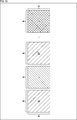
- the right part of FIG. 17 shows a configuration example within the range ZA of the imaging device 121 of FIG.
- the left part of FIG. 17 shows a configuration example of the pixel 121a in the range ZA.
- the range shown in black is the light shielding film 121b, and the light shielding range of each pixel 121a is determined, for example, according to the rule shown in the left part of FIG.
- the main light-shielding portion Z101 in the left part of FIG. 17 is a range in which light is shielded in common in each pixel 121a.
- the main light shielding portion Z101 has a height in the range of dx1 from the left side and the right side of the pixel 121a and in the range from the upper side and the lower side of the pixel 121a to the inside of the pixel 121a. It is the range of dy1.
- a rectangular opening Z111 which is not shielded by the light shielding film 121b is provided within the range Z102 inside the main light shielding portion Z101. Therefore, in each pixel 121a, the range other than the opening Z111 is shielded by the light shielding film 121b.
- the openings Z111 of the pixels 121a are regularly arranged. Specifically, the horizontal position of the opening Z111 in each pixel 121a is the same in the pixels 121a in the same vertical direction. Further, the position in the vertical direction of the opening Z111 in each pixel 121a is the same in the pixels 121a in the same horizontal row.
- the horizontal position of the opening Z111 in each pixel 121a is shifted at a predetermined interval according to the horizontal position of the pixel 121a. That is, as the position of the pixel 121a advances to the right, the left side of the opening Z111 moves to the position shifted to the right from the left side of the pixel 121a by the widths dx1, dx2,.
- the distance between the width dx1 and the width dx2, the distance between the width dx2 and the width dx3, ..., the distance between the width dxn-1 and the width dxn is the length obtained by subtracting the width of the opening Z111 from the width of the range Z102 Divided by the number of pixels n-1 in the horizontal direction.
- the position in the vertical direction of the opening Z111 in each pixel 121a is shifted at a predetermined interval according to the position in the vertical direction of the pixel 121a. That is, as the position of the pixel 121a moves downward, the upper side of the opening Z111 moves downward from the upper side of the pixel 121a by heights dy1, dy2,.
- the distance between the height dy1 and the height dy2, the distance between the height dy2 and the height dy3, ..., the distance between the height dyn-1 and the height dyn are respectively from the vertical height of the range Z102 to the opening Z111
- the length obtained by subtracting the height of the image is divided by the number of pixels m-1 in the vertical direction.
- the right part of FIG. 18 shows a configuration example within the range ZB of the imaging device 121 of FIG.
- the left part of FIG. 18 shows a configuration example of the pixel 121a 'in the range ZB.
- the range shown in black is the light shielding film 121b ', and the light shielding range of each pixel 121a' is determined, for example, according to the rule shown in the left part of FIG.
- the main light shielding portion Z151 at the left part of FIG. 18 is a range in which light is shielded in common in each pixel 121a '. Specifically, the main light shielding portion Z151 goes from the left side and the right side of the pixel 121a 'to the inside of the pixel 121a' and in the range of the width dx1 'and from the upper side and the lower side of the pixel 121a' And the height dy1 '.
- a rectangular opening Z161 which is not shielded by the light shielding film 121b' is provided in a range Z152 inside the main light shielding portion Z151. Therefore, in each pixel 121a ', the range other than the opening Z161 is shielded by the light shielding film 121b'.
- the opening Z161 of each pixel 121a ' is regularly arranged similarly to the opening Z111 of each pixel 121a of FIG. Specifically, the horizontal position of the opening Z161 in each pixel 121a 'is the same in the pixels 121a' in the same vertical direction. Further, the vertical position of the opening Z 161 in each pixel 121 a ′ is the same in the pixels 121 a ′ in the same horizontal row.
- the horizontal position of the opening Z161 in each pixel 121a ' is shifted at a predetermined interval in accordance with the horizontal position of the pixel 121a'. That is, as the position of the pixel 121a 'proceeds to the right, the left side of the opening Z161 moves to the position shifted to the right by the widths dx1', dx2 ', ..., dxn' from the left side of the pixel 121a '. Do.
- the length obtained by subtracting the width is divided by the number of pixels n-1 in the horizontal direction.
- the position in the vertical direction of the opening Z161 in each pixel 121a ' is shifted at a predetermined interval according to the position in the vertical direction of the pixel 121a'. That is, as the position of the pixel 121a 'moves downward, the upper side of the opening Z161 is shifted downward by height dy1', dy2 ', ..., dyn' from the upper side of the pixel 121a '.
- the distance between the height dy1 ′ and the height dy2 ′, the distance between the height dy2 ′ and the height dy3 ′,..., The distance between the height dyn ⁇ 1 ′ and the height dyn ′ are in the vertical direction of the range Z152
- the length obtained by subtracting the height of the opening Z161 from the height is divided by the number of pixels m-1 in the vertical direction.
- the length obtained by subtracting the width of the opening Z111 from the width of the range Z102 of the pixel 121a in FIG. 17 is the width of the opening Z161 from the width of the range Z152 of the pixel 121a ′ in FIG. It becomes larger than the width which I pulled. Therefore, the intervals of change in the widths dx1, dx2,..., Dxn in FIG. 17 are larger than the intervals of changes in the widths dx1 ', dx2',.
- the length obtained by subtracting the height of the opening Z111 from the height in the vertical direction of the range Z102 of the pixel 121a of FIG. 17 is the height of the opening Z161 in the vertical direction of the range Z152 of the pixel 121a ′ of FIG. It is larger than the length minus the height. Accordingly, the change intervals of the heights dy1, dy2... Dyn in FIG. 17 are larger than the change intervals of the heights dy1 ', dy2'.
- the interval of change of the position in the horizontal direction and the vertical direction of the opening Z111 of the light shielding film 121b of each pixel 121a of FIG. 17 and the horizontal direction of the opening Z161 of the light shielding film 121b ′ of each pixel 121a ′ of FIG. It is different from the interval of change of position in the direction and vertical direction.
- the difference in this interval is the difference in object resolution (angular resolution) in the restored image. That is, the change in the horizontal and vertical positions of the opening Z161 of the light shielding film 121b 'of each pixel 121a' in FIG. 18 corresponds to the horizontal direction of the opening Z111 of the light shielding film 121b in each pixel 121a of FIG.
- the restored image restored using the detection signal of each pixel 121a 'in FIG. 18 has a higher subject resolution than the restored image restored using the detection signal of each pixel 121a in FIG. Become.
- the imaging device 121 including pixels (having various incident angle directivity) of various angles of view is realized. It becomes possible.
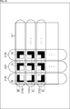
- the pixel 121a and the pixel 121a ′ are divided into the range ZA and the range ZB is described above, this is to simplify the description, and the pixels 121a corresponding to different angles of view are the same. It is desirable to be mixedly arranged in the area.
- each unit U is a pixel 121a-W with a wide angle of view, a middle angle of view
- pixels of a pixel 121a-M, a pixel 121a-N with a narrow angle of view, and a pixel 121a-AN with a very narrow angle of view are used.
- images of intermediate angles of view of four types of angle of view and images of angles of view before and after that may be generated by interpolation from images of four types of angle of view, and images of various angles of view are seamlessly generated By doing this, a pseudo optical zoom may be realized.
- all wide angle of view pixels may be used, or part of the wide angle of view pixels may be used.
- all narrow angle of view pixels may be used, or a part of narrow angle of view pixels may be used.
- Imaging processing by the imaging device 101 in FIG. 2 will be described with reference to the flowchart in FIG.
- step S1 the imaging element 121 captures an image of a subject.
- a detection signal indicating a detection signal level corresponding to the light amount of incident light from the subject is output from each pixel 121a of the imaging device 121 having different incident angle directivity, and the imaging device 121 detects each pixel 121a.
- the detection image composed of a signal is supplied to the restoration unit 122.
- step S2 the restoration unit 122 obtains a coefficient used for image restoration. Specifically, the restoration unit 122 sets the distance to the object plane 31 to be restored, that is, the object distance. Note that any method can be adopted as a method of setting the subject distance. For example, the restoration unit 122 sets the subject distance input by the user via the input unit 124 or the subject distance detected by the detection unit 125 as the distance to the subject plane 31 to be restored.
- the restoration unit 122 reads out from the storage unit 128 the coefficient set group associated with the set subject distance.
- step S3 the restoration unit 122 restores the image using the detected image and the coefficients. Specifically, the restoration unit 122 uses the detection signal level of each pixel of the detection image and the coefficient set group acquired in the process of step S2 to set the above-mentioned equation (1) to equation (3) or The simultaneous equations described with reference to equations (4) to (6) are created. Next, the restoration unit 122 calculates the light intensity of each point light source on the object plane 31 corresponding to the set object distance by solving the created simultaneous equations. Then, the restoration unit 122 arranges the pixels having pixel values according to the calculated light intensity according to the arrangement of the point light sources of the object plane 31 to generate a restored image on which the image of the object is formed.
- step S4 the imaging apparatus 101 performs various processes on the restored image.
- the restoration unit 122 performs demosaicing processing, ⁇ correction, white balance adjustment, conversion processing to a predetermined compression format, and the like on the restored image as necessary.
- the restoration unit 122 supplies, for example, a restored image to the display unit 127 for display, or supplies the restored image to the recording and reproduction unit 129, and records the restored image on the recording medium 130 as needed. , Output to other devices.
- the example of restoring the restored image from the detected image using the image sensor 121 and the coefficient set group associated with the subject distance has been described, but, for example, as described above in addition to the subject distance
- the set of coefficients corresponding to the angle of view of the restored image may be further prepared, and the set of coefficients corresponding to the subject distance and the angle of view may be used to restore the restored image.
- the resolution for the subject distance and the angle of view depends on the number of coefficient set groups prepared.
- the example using detection signals of all the pixels included in the detected image has been described, but the subject distance specified among the pixels constituting the image sensor 121 And a detection image consisting of detection signals of pixels having incident angle directivity corresponding to the angle of view may be generated and used to restore a restored image.
- Such processing enables the restored image to be restored with a detected image suitable for the subject distance and angle of view of the restored image to be obtained, and the restoration accuracy and image quality of the restored image are improved. That is, when the image corresponding to the specified subject distance and angle of view is, for example, an image corresponding to the angle of view SQ1 in FIG. 16, the pixel 121a having the incident angle directivity corresponding to the angle of view SQ1 is selected. By restoring the restored image with the detected image obtained from these, it is possible to restore the image of the angle of view SQ1 with high accuracy.
- the imaging device 101 having the imaging device 121 as an essential component in which each pixel is made to have incident angle directivity.
- the imaging lens, the pinhole, and the optical filter described in the above-mentioned patent documents and the like become unnecessary, it is possible to increase the degree of freedom in the design of the device, and configured separately from the imaging device 121
- it becomes unnecessary to use an optical element assumed to be mounted together with the imaging device 121 at the stage of configuring as an imaging device it becomes possible to realize miniaturization of the device with respect to the incident direction of incident light It is possible to reduce the cost.
- a lens corresponding to an imaging lens for forming an optical image such as a focus lens, is not necessary.
- a zoom lens for changing the magnification may be provided.
- a detection image is recorded, for example, without performing a decompression
- the restored image may be restored using a detected image at a desired timing.
- restoration of the restored image may be performed by the imaging device 101 or may be performed by another device.
- a restored image is obtained by solving simultaneous equations created using coefficient set groups according to an arbitrary subject distance and an angle of view, thereby obtaining an restored object for the object plane of an arbitrary subject distance and an angle of view. It is possible to realize refocusing and the like.
- the imaging apparatus 101 it is possible to restore the restored image of an arbitrary subject distance or angle of view by switching the coefficient set group in this manner, so the focal length (that is, object distance) or angle of view changes variously. This eliminates the need for processing such as repeated imaging while making it happen.
- the user switches the coefficient set group corresponding to different subject distance and angle of view, and displays the restored image on the display unit 127 while restoring the restored image of the desired subject distance and angle of view. It is also possible to get.
- Metadata is associated with the detected image. For example, metadata is added to image data including a detected image, the same ID is added to a detected image and metadata, or the detected image and metadata are recorded on the same recording medium 130. Metadata is associated.
- the detected image and the metadata can be recorded on different recording media, or can be output individually from the imaging apparatus 101.
- the metadata may or may not include the coefficient set group used for restoration.
- the subject distance and the angle of view at the time of restoration are included in the metadata, and at the time of restoration, a coefficient set group corresponding to the subject distance and the angle of view is acquired from the storage unit 128 or the like.
- the restored image is immediately restored at the time of imaging, it is possible to select, for example, an image to be recorded or output to the outside from among the detected image and the restored image.
- both images may be recorded or output to the outside, or only one of the images may be recorded or output to the outside.
- the presence or absence of restoration of a restored image and selection of an image to be recorded or output to the outside can be performed for each frame. For example, it is possible to switch the presence or absence of restoration of a restored image for each frame. In addition, for example, it is possible to individually switch the presence / absence of recording of the detected image and the presence / absence of recording of the restored image for each frame. Also, for example, while adding metadata to a detection image of a useful frame that may be used later, the detection images of all the frames may be recorded.
- an autofocus function as in an imaging apparatus using an imaging lens.
- the autofocus function can be realized by determining the optimum subject distance by the hill climbing method similar to the contrast AF (Auto Focus) method based on the restored image.
- the imaging device 121 is an essential component, and for example, the optical filter described in the above-mentioned patent documents and the like are not required. It is possible to realize an imaging device with high environmental resistance without distortion.
- the imaging lens, the pinhole, and the optical filter described in the above-mentioned patent documents and the like are not required, so the degree of freedom in design of a configuration having an imaging function is improved. It becomes possible.
- the processing by the restoration unit 122 is performed as the randomness of the difference in the light shielding range increases.
- the load on the Therefore, the processing load may be reduced by reducing the randomness by setting a part of the change in the light shielding range of the light shielding film 121b of each pixel 121a to be regular.
- the L-shaped light shielding film 121b is formed by combining the vertical band type and the horizontal band type, and the horizontal band type light shielding film 121b having the same width is combined in a predetermined column direction. In the row direction of, the vertical band type light shielding films 121b of the same height are combined.
- the light blocking range of the light blocking film 121b of each pixel 121a changes randomly in pixel units while having regularity in the column direction and the row direction.
- the difference in light blocking range of the light blocking film 121b of each pixel 121a that is, the randomness of the difference in incident angle directivity can be reduced, and the processing load of the restoration unit 122 can be reduced.
- the horizontal band type light shielding film 121b having the same width X0 is used for all pixels in the same column indicated by the range Z130.
- a vertical band type light shielding film 121b of the same height Y0 is used for the pixels in the same row indicated by the range Z150.
- an L-shaped light shielding film 121b in which these are combined is used for the pixels 121a specified in each row and column.
- the light shielding film 121b of the horizontal band type having the same width X1 is used, and the same row indicated by the range Z151 adjacent to the range Z150.
- the vertical band type light shielding film 121b of the same height Y1 is used for the pixel of.
- the light shielding film 121b of the horizontal band type having the same width X2 is used for all pixels in the same row indicated by the range Z152 adjacent to the range Z151.
- a vertical band type light shielding film 121b of the same height Y2 is used for the pixels 121a specified in each row and column.
- each element of matrix N of (N ⁇ N) rows ⁇ (N ⁇ N) rows of coefficient sets, and (N ⁇ N) rows ⁇ 1 row vector X representing a restored image It is shown that the result of multiplication of is a vector Y of (N ⁇ N) rows ⁇ 1 column representing a detected image. Then, from this relationship, simultaneous equations corresponding to, for example, the above-described Equation (1) to Equation (3) or Equation (4) to Equation (6) are configured.
- each element of the first column indicated by the range Z201 of the matrix A corresponds to an element of the first row of the vector X
- an N ⁇ N column indicated by the range Z202 of the matrix A Indicates that each element of X corresponds to an element of the N ⁇ Nth row of the vector X.
- the matrix A is a diagonal matrix in which all the down-tilting diagonal components become one.
- the matrix A does not form a diagonal matrix.
- the restored image is obtained by solving the simultaneous equations based on the determinant shown in FIG. 22 and finding each element of the vector X.
- the matrix A can not be accurately determined, the matrix A can not be accurately measured, the basis vector of the matrix A can not be solved in the case near linear dependence, and each element of the detected image It contains noise. And it may not be possible to solve simultaneous equations by any of those reasons or their combination.
- a t is the transposed matrix of the matrix A
- I is the identity matrix
- the matrix A the matrix AL of N rows ⁇ N columns, decomposed into matrix AR T of N rows ⁇ N columns, N rows ⁇ N columns, each representing a restored image
- the result obtained by multiplying the former stage and the latter stage of the matrix X of X is made to be an N-row ⁇ N-column matrix Y representing a detected image.
- matrix AL of number of elements is (N ⁇ N)
- AR T the number of elements of each matrix is 1 / (N ⁇ N).
- a matrix matrix AL in parentheses of formula (8) is realized by an inverse matrix of the transposed matrix of the matrix A and matrix AR T.
- the element group Z222 is obtained by multiplying each element group Z221 of the corresponding column of the matrix AL by the element of interest Xp in the matrix X Be Further, by multiplying the elements in the row corresponding to the element of interest Xp the element group Z222 matrix AR T, 2-dimensional response Z224 that corresponds to the element of interest Xp is calculated. Then, the two-dimensional response Z 224 corresponding to all elements of the matrix X is integrated to obtain the matrix Y.
- the matrix can be made smaller, the capacity of the memory used for calculation can be reduced, and the device cost can be reduced.
- FIG. 21 shows an example in which the light shielding range (light receiving range) is changed in pixel units while giving predetermined regularity in the horizontal direction and the vertical direction, but in the present disclosure, such an example is shown.
- the light blocking range (light receiving range) is not completely randomly set in a pixel unit, it is considered that the light blocking range (light receiving range) is also set randomly at some random settings. In other words, in the present disclosure, not only when the light blocking range (light receiving range) is completely set randomly on a pixel basis, but also to a certain degree random (for example, regularity for some of all pixels).
- Embodiment >> Next, an embodiment of the present disclosure will be described with reference to FIGS. 26 to 35.
- the imaging device 121 using pixels having incident angle directivity an imaging lens, an optical filter, and the like are not necessary, so the degree of freedom of arrangement of the pixels 121a is high.
- an object is imaged by a plurality of imaging devices respectively provided with imaging elements having incident angle directivity, and a restored image is restored using detection signals obtained by each imaging device.
- FIG. 26 is a block diagram showing a configuration example of an imaging system 301 according to an embodiment of the present disclosure.
- the imaging system 301 includes an imaging device group 311 and a signal processing device 312 configured as separate housings.
- the imaging device group 311 includes two or more n imaging devices 321-1 to 321-n.
- the imaging devices 321-1 to 321-n are simply referred to as imaging devices 321 when it is not necessary to distinguish them individually.
- Each imaging device 321 is installed at a predetermined position and direction using, for example, a jig or the like. Alternatively, each imaging device 321 may be appropriately installed, and the position and orientation of each imaging device 321 may be detected by a predetermined method. In addition, each imaging device 321 includes the imaging element 121 having the incident angle directivity described above, generates an image file including a detection signal set including a detection signal output from each pixel 121 a of each imaging element 121, and outputs a signal Transmit to processing unit 312.
- the image file is a data set that includes image data, and optionally includes metadata corresponding to the image data.
- the image data includes, for example, at least one of a detection signal set, a detection image, or a restored image.
- the metadata includes, for example, an ID for identifying each imaging device 321, a coefficient set group corresponding to image data, and the like.
- the signal processing device 312 controls imaging by each imaging device 321, acquires an image file from each imaging device 321, and performs restoration processing and the like of a restored image using the acquired image file.
- FIG. 27 is a block diagram showing a configuration example of the imaging device 321 of FIG. In the figure, parts corresponding to those of the imaging apparatus 101 in FIG. 2 are assigned the same reference numerals, and the description thereof will be omitted as appropriate.
- the imaging device 321 includes an imaging element 121, a control unit 411, an association unit 413, a storage unit 414, and a communication unit 414. Further, a signal processing control unit 401 is configured by the control unit 411, the association unit 413, the storage unit 414, and the communication unit 414. Note that the imaging device 321 does not include an imaging lens.
- the imaging device 121, the control unit 411, the association unit 413, the storage unit 414, and the communication unit 414 are connected to one another via the bus B2, and transmit and receive data via the bus B2.
- the description of the bus B2 in the case where each unit of the imaging device 321 transmits and receives data via the bus B2 is omitted.
- the imaging element 121 outputs a detection signal set including the detection signal output from each pixel 121a to the bus B2.
- the control unit 411 includes, for example, various processors, and controls each unit of the imaging device 321.
- the input unit 412 includes an input device (for example, a key, a switch, a button, a dial, a touch panel, a remote controller, and the like) for performing an operation of the imaging device 321, an input of data used for processing, and the like.
- the input unit 412 outputs an operation signal, input data, and the like to the bus B2.
- the association unit 413 associates the detection signal set obtained by the imaging device 121 with the metadata corresponding to the detection signal set in cooperation with the association unit 504 (FIG. 29) of the signal processing device 312 or independently. Do.
- the storage unit 414 includes one or more storage devices such as a read only memory (ROM), a random access memory (RAM), and a flash memory, and stores, for example, programs and data used for processing of the imaging device 321.
- ROM read only memory
- RAM random access memory
- flash memory stores, for example, programs and data used for processing of the imaging device 321.
- the storage unit 414 stores an ID for uniquely identifying the imaging device 321.
- the communication unit 415 communicates with another device (for example, the other imaging device 321, the signal processing device 312, and the like) by a predetermined communication method.
- the communication method of the communication unit 415 may be wired or wireless. Further, the communication unit 415 can also correspond to a plurality of communication methods.
- FIG. 28 shows an example of the pattern of the light shielding film 121b in the pixel array portion of the imaging device 121-1 of the imaging device 321-1 to the imaging device 121-n of the imaging device 321-n.
- the light shielding film 121b is disposed so as to surround four sides, and a rectangular opening is provided in the pixel 121a.
- the openings are set to the same size in all the pixels 121 a in the same imaging element 121, and are set to different sizes among the pixels 121 a of different imaging elements 121. Further, the positions of the openings of the respective pixels 121 a in the same image sensor 121 are all different. Therefore, at least one of the sizes and positions of the openings is different among all the pixels 121a of the imaging elements 121-1 to 121-n, and the incident angle directivity of all the pixels 121a is different from each other.
- imaging is performed by a plurality of imaging devices 321 each having different incident angle directivity.
- the number of equations constituting the simultaneous equations used for restoration of the restored image can be increased.
- the number of pixels of the restored image can be increased, and the resolution of the restored image is improved.
- the incident angle directivity of all the pixels 121 a does not necessarily have to be different, and some of them may be the same. However, the smaller the number of pixels 121a having the same incident angle directivity, the more the number of equations constituting the simultaneous equations used for restoration of the restored image can be increased, and the number of pixels of the restored image can be increased. The resolution of the image is improved.
- FIG. 29 is a block diagram showing a configuration example of the signal processing device 312 of FIG.
- the signal processing device 312 includes a restoration unit 501, a control unit 502, an input unit 503, an association unit 504, a display unit 505, a storage unit 506, a recording and reproduction unit 507, a recording medium 508, and a communication unit 509.
- the restoration unit 501, the control unit 502, the input unit 503, the display unit 505, the storage unit 506, the recording and reproduction unit 507, and the communication unit 509 are mutually connected via the bus B3, and data are connected via the bus B3.
- Send and receive In the following, in order to simplify the description, the description of the bus B3 in the case where each part of the signal processing device 312 transmits and receives data via the bus B3 is omitted.
- the restoration unit 501 performs restoration processing and the like of a restored image by the same processing as the restoration unit 122 of the imaging device 101 in FIG. 2 using the detection signal set included in the image file received from each of the imaging devices 321.
- the restoration unit 501 outputs the restored image to the bus B3.
- the control unit 502 includes, for example, various types of processors, and controls each unit of the signal processing device 312.
- the input unit 503 includes an input device (for example, a key, a switch, a button, a dial, a touch panel, a remote controller, and the like) for performing an operation of the signal processing apparatus 312, an input of data used for processing, and the like.
- the input unit 503 outputs an operation signal, input data, and the like to the bus B3.
- the associating unit 504 associates the detection signal set acquired from each imaging device 321 with the metadata corresponding to each detection signal set in cooperation with the associating unit 413 of the imaging device 321 or by itself.
- the display unit 505 includes, for example, a display, and displays various types of information (for example, a restored image and the like). Note that the display unit 505 may include an audio output unit such as a speaker to output audio.
- the storage unit 506 includes one or more storage devices such as a ROM, a RAM, and a flash memory, and stores, for example, programs and data used for the processing of the signal processing device 312.
- the storage unit 506 stores installation information regarding the installation state of each imaging device 321.
- the installation information includes, for example, information on the position and the orientation of the light receiving surface of the imaging device 121 of each imaging device 321.
- the installation information is created at the time of installation of the imaging device 321 or the like, and stored in the storage unit 506.
- each imaging device 321 detects its own installation state using a position sensor such as GNSS (Global Navigation Satellite System) or a direction sensor, and transmits the detection result to the signal processing device 312, and as a signal
- the processing device 312 may generate the installation information based on the information received from each imaging device 321.
- the signal processing device 312 or another device detects the installation state of each imaging device 321 based on an image or the like obtained by imaging each imaging device 321, and generates installation information based on the detection result. May be
- the storage unit 506 stores a coefficient set group corresponding to each imaging element 121 of each imaging device 321.
- the setting method of the coefficient corresponding to each image pick-up element 121 of each imaging device 321 is later mentioned with reference to FIG. 30 thru
- the recording and reproducing unit 507 performs recording of data on the recording medium 508 and reproduction (reading) of data recorded on the recording medium 508.
- the recording / reproducing unit 507 records the restored image on the recording medium 508 or reads it from the recording medium 508.
- the recording / reproducing unit 507 records the detection signal set and the corresponding metadata on the recording medium 508 or reads out from the recording medium 508.
- the recording medium 508 is, for example, an HDD, an SSD, a magnetic disk, an optical disk, a magneto-optical disk, a semiconductor memory or the like, or a combination thereof.
- the communication unit 509 communicates with another device (for example, each imaging device 321 or the like) by a predetermined communication method.
- the communication method of the communication unit 509 may be either wired or wireless.
- the communication unit 509 can also correspond to a plurality of communication methods.
- the imaging elements 121-1 to 121-n are arranged such that the respective light receiving surfaces are arranged in the same straight line in the same plane. Further, the point light source P of the subject is present at a position separated by the distance Ds1 from the center of the line formed by the light receiving surface of each of the imaging elements 121.
- Dw the distance from the left end of the light receiving surface of the imaging element 121-1 in the drawing to the right end of the light receiving surface of the imaging element 121-n.
- an angle ⁇ w indicating the range of the incident light incident on each imaging element 121 is expressed by the following expression (9).
- the restored images are adjacent
- the angular resolution between pixels is 0.04 degrees.
- a distance Ds1 at which the angle ⁇ w in Equation (9) is equal to or less than 0.04 degrees which is an angular resolution between adjacent pixels in the restored image can be regarded as infinity.
- the point light source P can be regarded as existing at infinity if the following equation (10) is satisfied.
- incident light from each point light source of the subject can be regarded as parallel light, and the incident angle of incident light from each point light source to each pixel 121a of each imaging element 121 is , All become equal.
- incident light from a point light source PA existing at infinity with respect to the pixels 121a-1 and 121a-2 at distant positions can be regarded as parallel light, and The incident angle is the same between the pixel 121a-1 and the pixel 121a-2.
- the incident light from the point light source PB existing at infinity with respect to the pixel 121a-1 and the pixel 121a-2 can be regarded as parallel light, and the incident angles at the pixel 121a-1 and the pixel 121a-2 Will be the same.
- the incident angle of the incident light from each point light source of the subject existing at infinity does not change depending on the position of (the image pickup element 121 of) each image pickup device 321.
- the range Ws (angle of view) between the point light source PA and the point light source PB where the pixel 121a-1 and the pixel 121a-2 can receive incident light is, as described above with reference to FIG. It becomes settled by the light shielding range etc. of 121a.
- the incident angle of the incident light from the point light source PA of the object plane 31 present at a distance closer than infinity (a distance less than infinity) is determined by the imaging element 121 of each imaging device 321. It depends on the position. More strictly, the incident angle of the incident light from the point light source PA differs depending on the position of each pixel 121 a of each imaging element 121. Specifically, the incident angle ⁇ 1 of the incident light incident on each pixel 121a from the point light source PA is expressed by the following equation (12).
- Ds2 is the distance between the object plane 31 and the light receiving surface of each image sensor 121.
- Xa is the position of the point light source PA in the object plane 31
- Xp is the position of the pixel 121a in a plane parallel to the object plane 31
- Xa-Xp is the point light source PA in the direction parallel to the object plane 31 It is the distance between the pixel 121a.
- white circles on the object surface 31 schematically indicate the positions of the point light sources, and shaded dots on the light receiving surfaces of the imaging device 121-1 and the imaging device 121-n are The position of the pixel 121a is schematically shown.
- the incident angle ⁇ 1 varies with the subject distance Ds2 and the relative position (Xa ⁇ Xp) of the point light source PA and the pixel 121a. Therefore, the incident angle from the point light source of the subject present at a distance closer than infinity changes depending on the subject distance and the position of the imaging device 321 (the image sensor 121 thereof).
- the orientation of the imaging device 321, more accurately, of the imaging device 121 of the imaging device 321 with respect to the subject changes depending on the orientation of the light receiving surface.
- the point light source PA to each pixel 121a of the imaging element 121-n.
- the incident angle ⁇ 2 of incident light is expressed by the following equation (13).
- ⁇ 2 atan ((Xa ⁇ Xp) / Ds2) + ⁇ r ... (13)
- the incident angle ⁇ 2 is an angle obtained by adding the inclination ⁇ r of the light receiving surface of the image sensor 121-n with respect to the object surface 31 to the incident angle ⁇ 1 of equation (12). This is the same as when the subject is at infinity.
- the coefficient set group corresponding to each imaging element 121 of each imaging device 321 with respect to the subject existing at infinity changes depending on the direction of the light receiving surface of the imaging element 121 with respect to the object surface to be restored.
- the coefficient set group in each imaging element 121 of each imaging device 321 for an object located at a distance closer than infinity, the subject distance with respect to the object plane to be restored, and the position and orientation of the light receiving surface Depending on the
- the coefficient set group corresponding to each imaging element 121 of each imaging device 321 is the subject distance of the subject plane to be restored, and the subject plane. It is set for each combination of orientation (hereinafter referred to as subject direction). Then, for example, a coefficient set group corresponding to each image sensor 121 is prepared for each combination of subject distance and subject direction, and stored in the storage unit 506.
- step S101 the signal processing device 312 transmits an imaging command.
- the control unit 502 generates an imaging command, and transmits the imaging command to each imaging device 321 via the communication unit 509.
- Each imaging device 321 receives an imaging command in step S151 of FIG. 35 described later, and transmits an image file in step S153.
- Each image file includes, for example, an ID for identifying each imaging device 321, and a detection signal set obtained by the imaging element 121 of each imaging device 321.
- step S102 the communication unit 509 receives the image file transmitted from each imaging device 321.
- the communication unit 509 supplies the received image file to the restoration unit 501.
- the restoration unit 501 obtains a coefficient used for image restoration. Specifically, the restoring unit 501 sets a combination of the distance (subject distance) and the direction (subject direction) to the subject plane 31 to be restored. An arbitrary method can be adopted as a setting method of the combination of the subject distance and the subject direction. For example, the restoration unit 501 sets the subject distance and the subject direction input by the user via the input unit 503 as a combination of the subject distance and the subject direction of the subject surface 31 to be restored.
- the restoration unit 501 reads out from the storage unit 506 the coefficient set group associated with the combination of the set subject distance and subject direction.
- step S104 the reconstruction unit 501 reconstructs one image using the detection signal set and the coefficient. That is, the restoration unit 501 performs a process similar to the process performed by the restoration unit 122 of the imaging apparatus 101 in step S3 of FIG. 20, thereby setting a plurality of detection signal sets included in the image file received from each imaging apparatus 321; One restored image is restored using one simultaneous equation using the coefficient set group obtained by the processing of
- step S105 the signal processing device 312 performs various processes on the restored image. That is, the signal processing device 312 performs various processing on the restored image by the same processing as the imaging device 101 in step S4 of FIG.
- step S151 the communication unit 415 receives the imaging command transmitted from the signal processing device 312 in step S101 of FIG.
- the communication unit 415 supplies the received imaging command to the control unit 411.
- step S152 the imaging element 121 captures an image of a subject, as in the process of step S1 in FIG.
- the imaging element 121 supplies the detection signal set including the detection signal of each pixel 121a to the associating unit 413.
- the imaging device 321 transmits an image file.
- the association unit 413 generates an image file including the ID of the imaging device 321 and the detection signal set acquired from the imaging device 121.
- the detection signal set is associated with the ID of the imaging device 321.
- the association unit 413 transmits the generated image file to the signal processing apparatus 312 via the communication unit 415.
- the number of pixels of the restored image can be increased as compared with the case where imaging is performed by only one imaging device 321, and the image quality of the restored image, more specifically, the resolution of the restored image can be improved. it can.
- each imaging element 121 of each imaging device 321 can be reduced and the size thereof can be reduced.
- the number of pixels of the restored image can be increased by increasing the number of imaging devices 321 without increasing the number of pixels of each imaging device 121 of each imaging device 321. Therefore, for example, there is no need to introduce a new manufacturing apparatus or the like due to the enlargement of the imaging device 121, and the manufacturing cost can be reduced.
- each imaging device 321 can be miniaturized, the degree of freedom of arrangement of each imaging device 321 is improved, and the application range of the imaging device 321 can be expanded, for example, in the field of IoT (Internet of Things) .
- IoT Internet of Things
- a coefficient set group corresponding to the angle of view of the restored image is further prepared, and further using the coefficient set group corresponding to the angle of view May be restored.
- FIG. 28 shows an example in which the pattern of the light shielding film 121b of the imaging device 121 of each imaging device 321 is different, for example, as shown in FIG. 36, the same imaging device 121 is used for each imaging device 321.
- the pattern of the light shielding film 121b of the imaging element 121 may be the same. In this case, imaging is performed by a plurality of imaging devices 321 having the same incident angle directivity.
- coefficient set groups corresponding to the respective imaging elements 121 are all the same for an object at infinity. Therefore, since the equations constituting the simultaneous equations used for restoring the restored image overlap, and the number of expressions can not be increased, the number of pixels of the restored image can not be increased. However, it is assumed that the detection signal levels are different between the pixels 121 a at the same position of the respective imaging elements 121 due to the influence of noise or the like. As a result, in the equations (for example, Equations (1) to (6) described above) corresponding to the pixel 121a at the same position of each imaging device 121, even if the right side overlaps, the detection signal level on the left side is different. become.
- the incident angle of the incident light from the subject to each imaging element 121 is different, so the coefficient set group corresponding to each imaging element 121 is different. Therefore, the number of equations constituting the simultaneous equations used to restore the restored image can be increased, and the number of pixels of the restored image can be increased.
- the incident angle directivity of some of the imaging elements 121 may be the same, and the incident angle directivity of some of the imaging elements 121 may be different.
- ⁇ Modification concerning coefficient> when the position and the orientation of each imaging device 321 are variable, as described above with reference to FIGS. 32 and 33, the coefficient set group corresponding to each imaging element 121 corresponds to the subject distance and the subject direction.
- the position and the orientation of the imaging device 321, and more precisely, the position and the orientation of the light receiving surface of the imaging element 121 of the imaging device 321 are different. Therefore, when the position and the orientation of each imaging device 321 are variable, for example, each combination of the subject distance and the subject direction, and the position and orientation of the imaging device 121 of each imaging device 321 corresponds to each imaging device 121
- a coefficient set group may be prepared.
- the restoration unit 501 sets the coefficient set group corresponding to the imaging device 121 of each imaging device 321.
- the restored image may be restored using the coefficient set read out from the storage unit 506 and read out.
- the restoration unit 501 may be calculated using the characteristics of the weight Wx and the weight Wy described above with reference to 9.
- each imaging device 321 detects the installation state including the position and orientation at the time of imaging of each imaging device 321, and includes metadata including the detection result in the image file and transmits it to the signal processing device 312 You may Alternatively, for example, the installation state of each imaging device 321 may be detected based on an image or the like obtained by imaging the imaging device 321 by the signal processing device 312 or another device.
- each imaging device 321 includes metadata including a coefficient set group corresponding to the subject distance, subject direction, and angle of view. May be included in the image file and transmitted to the signal processing device 312.
- FIG. 37 shows a configuration example of an imaging system 601 which is a first modified example of the imaging system.
- parts corresponding to those of the imaging system 301 in FIG. 26 are assigned the same reference numerals, and the description thereof will be omitted as appropriate.
- the imaging system 601 is different from the imaging system 301 of FIG. 26 in that an imaging device group 611 is provided instead of the imaging device group 311 and the signal processing device 312 is deleted.
- the imaging device group 611 is different from the imaging device group 311 in that an imaging device 621 is added.
- the imaging device 621 has, for example, the same configuration as the imaging device 101 in FIG. Then, the imaging device 621 transmits an imaging command to each imaging device 321 as in the signal processing device 312 of FIG. 26, and controls imaging of the subject by each imaging device 321, and also images itself of the subject itself. Do. Then, the imaging device 621 receives an image file from each imaging device 321, and uses one of the detection signal set included in the received image file and the detection signal set acquired by imaging by oneself, one restored image Restore the
- the number of imaging devices 321 may be one.
- FIG. 38 shows a configuration example of an imaging system 651 which is a second modified example of the imaging system.
- parts corresponding to those of the imaging system 301 in FIG. 26 are assigned the same reference numerals, and the description thereof will be omitted as appropriate.
- the imaging system 651 is different from the imaging system 301 of FIG. 26 in that an imaging device group 661 is provided instead of the imaging device group 311.
- the imaging device group 661 differs from the imaging device group 311 in that an imaging device 671 is added.
- the imaging device 671 has, for example, the same configuration as the imaging device 321 in FIG. Then, as with the signal processing device 312 shown in FIG. 26, the imaging device 671 transmits an imaging command to each imaging device 321 to control the imaging of the subject by each imaging device 321, and also performs imaging of the subject itself. Do. Then, the imaging device 621 receives an image file from each imaging device 321, and receives an image file received from each imaging device 321, and an image file including a detection signal set acquired by imaging by itself. Send to That is, the imaging device 621 plays a role of relaying the image file from each imaging device 321 to the signal processing device 312.
- the signal processing device 312 restores the restored image using the detection signal data included in each of the received image files.
- the number of imaging devices 321 may be one.
- the imaging system 301 the imaging system 601, and the imaging system 651
- the imaging devices 321 synchronously perform imaging in accordance with an external command.
- imaging may be performed synchronously, or each imaging device 321 may individually perform imaging without synchronization.
- FIG. 39 shows a configuration example of an imaging device 701 provided with a plurality of imaging elements 121.
- parts corresponding to those of the imaging device 101 in FIG. 2 are assigned the same reference numerals, and the description thereof will be omitted as appropriate.
- the imaging device 701 is different from the imaging device 101 of FIG. 2 in that the imaging device 701 includes an imaging unit 711 including two or more n imaging devices 121-1 to 121-n.
- Each imaging element 121 supplies a detection signal set obtained by imaging a subject to the restoration unit 122 or outputs the same to the bus B1.
- the restoration unit 122 restores a restored image using the detection signal set acquired from each imaging element 121.
- Each imaging element 121 is installed in the housing of the imaging device 701.
- the imaging device 621 in FIG. 37, and the imaging device 671 in FIG. It is possible to do so.
- restoration image was shown using the several detection signal set obtained by imaging using the several imaging device 121 from which an installation state differs, the same, for example
- the restored image may be restored using a plurality of detection signal sets obtained by imaging the imaging device 121 in a plurality of installation states in which at least one of the position and the orientation with respect to the subject is different.
- the image pickup device 121 or an image pickup apparatus including the image pickup device 121 may restore a restored image using a plurality of detection signal sets obtained by imaging the same subject while moving. .
- the imaging device 121 or the imaging device including the imaging device 121 restores a restored image using a plurality of detection signal sets obtained by imaging while changing the direction to the subject at the same position. You may do so.
- the imaging device 121 or the imaging device including the imaging device 121 restores the restored image using a plurality of detection signal sets obtained by imaging while changing the distance to the subject. It is also good.
- each detection signal set is associated with metadata corresponding to each detection signal set, and a restored image is restored using each detection signal set at a desired timing after imaging.
- detection signals can be obtained by putting the detection signal set and the metadata in the same image file, assigning the same ID to the detection signal set and the metadata, or recording the detection signal set and the metadata on the same recording medium.
- Sets are associated with metadata.
- the detection signal set and the metadata may be recorded by each imaging device that has performed imaging of a subject, or may be performed by a signal processing device or an imaging device that restores an image.
- the detection signal set and the metadata are recorded by each imaging device that has performed imaging of the subject, for example, a signal processing device or imaging that restores an image through the recording medium by the recorded detection signal set and the metadata. It is supplied to the device.
- the metadata may or may not include the coefficient set group used for restoration.
- the coefficient set group used for restoration for example, one or more of the subject distance at the time of restoration, the subject direction, and the angle of view, and the installation state of the imaging device or the imaging device at the time of imaging are included in the metadata.
- the user may transmit an imaging command to each imaging device 321 using a remote controller or the like.
- each imaging device 321 captures a still image of a subject without motion
- each imaging device 321 captures an image at an arbitrary timing without using an imaging command, or the input unit 124 of each imaging device 321.
- the imaging command may be individually generated and supplied to the control unit 123 in the same apparatus.
- ⁇ Modification Example Regarding Imaging Element 121> As the shape of the light shielding film 121b of each pixel 121a, it is possible to adopt a shape other than the above-described horizontal band type, vertical band type, L-shaped type, and a type provided with a rectangular opening.
- one pixel output unit may include nine photodiodes 121 f.
- the photodiodes 121f-11, 121f-114, 121f-117 to 121f-119 are substantially made.
- An incident angle characteristic similar to that of the pixel 121a provided with the L-shaped light shielding film 121b in which the light shielding film 121b is set in the range of -117 to 121f -119 can be obtained.
- the incident angle directivity can be changed as in the case where the position and the range shielded by the light shielding film 121 b are changed.
- one pixel output unit is configured by one pixel 121a.
- one pixel output unit may be configured by a plurality of pixels 121a.
- each of the pixels 121 a-111 to 121 a-119 includes, for example, one photodiode and does not include an on-chip lens.
- the incident angle directivity of the pixel output unit 801b can be realized.
- the pixel signals of the pixels 121a-112, 121a-113, 121a-115, and 121a-116 are added to generate a detection signal, and the pixels 121a-111, 121a-114, and It is possible to obtain the same incident angle directivity as in the case where the L-shaped light shielding film 121b is provided in the range of the pixels 121a-117 to the pixels 121a-119.
- the incident angle directivity can be set to different values as in the case where the position and the range shielded by the light shielding film 121b are changed.
- a pixel output unit 801 s can be configured by pixels 121 a-111, pixels 121 a-112, pixels 121 a-114, and pixels 121 a in 2 rows ⁇ 2 columns including the pixels 121 a-115.
- the range of the pixel output unit later by recording the pixel signals of all the pixels 121 a and setting the combination of the pixels 121 a later. Furthermore, it is possible to set the incident angle directivity of a pixel output unit later by selecting the pixel 121a which adds a pixel signal to a detection signal among the pixels 121a in the set pixel output unit.
- FIG. 4 illustrates an example in which different incident angle directivity is given to each pixel by using the light shielding film 121b as the modulation element or changing the combination of photodiodes contributing to the output. Then, for example, as shown in FIG. 42, it is also possible to use an optical filter 902 covering the light receiving surface of the imaging element 901 as a modulation element so that each pixel has incident angle directivity.
- the optical filter 902 is disposed to cover the entire surface of the light receiving surface 901A at a predetermined interval from the light receiving surface 901A of the imaging element 901.
- the light from the subject surface 31 is modulated by the optical filter 902, and then enters the light receiving surface 901 ⁇ / b> A of the image sensor 901.
- optical filter 902BW having a black and white lattice pattern shown in FIG.
- a white pattern portion that transmits light and a black pattern portion that blocks light are randomly disposed.
- the size of each pattern is set independently of the size of the pixel of the image sensor 901.
- FIG. 44 shows the light receiving sensitivity characteristics of the image sensor 901 with respect to light from the point light source PA and the point light source PB on the object plane 31 when the optical filter 902BW is used.
- the light from the point light source PA and the light from the point light source PB are respectively modulated by the optical filter 902BW, and then enter the light receiving surface 901A of the imaging element 901.
- the light reception sensitivity characteristic of the image pickup device 901 with respect to the light from the point light source PA becomes like a waveform Sa. That is, since a shadow is generated by the black pattern portion of the optical filter 902BW, a light and dark pattern is generated in the image on the light receiving surface 901A for the light from the point light source PA.
- the light receiving sensitivity characteristic of the image sensor 901 with respect to the light from the point light source PB becomes like a waveform Sb. That is, since a shadow is generated by the black pattern portion of the optical filter 902BW, a light and dark pattern is generated in the image on the light receiving surface 901A for the light from the point light source PB.
- each pixel of the image sensor 901 has incident angle directivity with respect to each point light source of the object plane 31.
- the optical filter 902HW of FIG. 45 may be used instead of the black pattern portion of the optical filter 902BW.
- the optical filter 902HW includes a linear polarization element 911A and a linear polarization element 911B having the same polarization direction, and a half wave plate 912.
- the half wave plate 912 is between the linear polarization element 911A and the linear polarization element 911B. It is pinched.
- a polarized portion shown by oblique lines is provided, and the white pattern portion and the polarized portion are randomly arranged.
- the linear polarization element 911A transmits only light of a predetermined polarization direction out of substantially non-polarized light emitted from the point light source PA.
- the linear polarization element 911A transmits only light whose polarization direction is parallel to the drawing.
- the polarized light transmitted through the linear polarizing element 911A the polarized light transmitted through the polarizing portion of the half-wave plate 912 is changed in polarization direction in a direction perpendicular to the drawing as the plane of polarization is rotated.
- the linear polarization element 911A transmits the polarized light transmitted through the white pattern portion, and hardly transmits the polarized light transmitted through the polarized portion. Therefore, the quantity of polarized light transmitted through the polarizing section is smaller than that of polarized light transmitted through the white pattern section. As a result, a pattern of shading similar to that in the case of using the optical filter BW is generated on the light receiving surface 901A of the imaging element 901.
- an optical interference mask can be used as the optical filter 902LF.
- the light emitted from the point light sources PA and PB of the object plane 31 is irradiated onto the light receiving surface 901A of the imaging element 901 through the optical filter 902LF.
- corrugation of a wavelength grade is provided in the light-incidence surface of optical filter 902LF.
- the optical filter 902LF maximizes transmission of light of a specific wavelength emitted from the vertical direction.
- the optical path length changes.
- the light weakens when the optical path length is an odd multiple of a half wavelength, and the light strengthens when an even multiple of a half wavelength. That is, the intensity of the transmitted light of the specific wavelength emitted from the point light sources PA and PB and transmitted through the optical filter 902LF is modulated according to the incident angle with respect to the optical filter 902LF as shown in B of FIG.
- the light is incident on the light receiving surface 901A. Therefore, the detection signal output from each pixel output unit of the imaging element 901 is a signal obtained by combining the light intensity after modulation of each point light source for each pixel output unit.
- the present disclosure can be applied to an imaging device and an imaging element that perform imaging of light of wavelengths other than visible light such as infrared light.
- the restored image is not an image that allows the user to visually recognize the subject, but is an image in which the user can not visually recognize the subject.
- the image quality of the restored image is improved with respect to the image processing apparatus or the like that can recognize the subject.
- the present technology since it is difficult for the normal imaging lens to transmit far infrared light, the present technology is effective, for example, when imaging far infrared light. Therefore, the restored image may be an image of far infrared light, and may be an image of other visible light or non-visible light without being limited to far infrared light.
- the series of processes described above can be performed by hardware or software.
- a program that configures the software is installed on a computer.
- the computer includes a computer (for example, the control unit 123 or the like) incorporated in dedicated hardware.
- the program executed by the computer can be provided by being recorded in, for example, a recording medium (eg, the recording medium 130 or the like) as a package medium or the like. Also, the program can be provided via a wired or wireless transmission medium such as a local area network, the Internet, or digital satellite broadcasting.
- a recording medium eg, the recording medium 130 or the like
- the program can be provided via a wired or wireless transmission medium such as a local area network, the Internet, or digital satellite broadcasting.
- the program executed by the computer may be a program that performs processing in chronological order according to the order described in this specification, in parallel, or when necessary, such as when a call is made. It may be a program to be processed.
- the present technology can have a cloud computing configuration in which one function is shared and processed by a plurality of devices via a network.
- each step described in the above-described flowchart can be executed by one device or in a shared manner by a plurality of devices.
- the plurality of processes included in the one step can be executed by being shared by a plurality of apparatuses in addition to being executed by one apparatus.
- the present disclosure can also have the following configurations.
- a plurality of pixel output units each receiving incident light from an object incident without passing through either the imaging lens or the pinhole, and outputting one detection signal indicating an output pixel value modulated by the incident angle of the incident light
- a plurality of images obtained in a plurality of states in which at least one of the position and the direction with respect to the subject is different by an imaging device that outputs a detection signal set including the plurality of detection signals output from the plurality of pixel output units.
- a signal processing apparatus comprising: a restoration unit that restores one restored image using a detection signal set.
- the restoration unit restores the one restored image using the plurality of detection signal sets and a coefficient set group selected based on a distance between each of the plurality of imaging elements and the subject.
- the signal processing apparatus as described in (2).
- the restoration unit is a coefficient set group selected based on both the distance and the position of each of the image sensors with respect to the subject when the distance between each of the image sensors and the object is less than a predetermined distance.
- the signal processing apparatus according to (3) wherein the one restored image is restored using the plurality of detection signal sets.
- the restoration unit uses the coefficient set group selected based on the distance, the position, and the orientation of each of the image sensors with respect to the subject, and the plurality of detection signal sets to perform the one restored image.
- the restoration unit restores the one restored image using one simultaneous equation using the plurality of detection signal sets and the coefficient set group, The signal according to any one of (3) to (5) Processing unit.
- the restoration unit is obtained by a detection signal set obtained by the at least a part of the imaging devices provided in the signal processing device, and an imaging device different from the imaging device provided in the signal processing device The signal processing apparatus according to (7), wherein the one restored image is restored using the set of detected signals.
- a plurality of pixel output units each receiving incident light from an object incident without passing through either the imaging lens or the pinhole, and outputting one detection signal indicating an output pixel value modulated by the incident angle of the incident light
- One or more imaging devices that output a detection signal set including a plurality of the detection signals output from the plurality of pixel output units;
- An imaging device comprising: an associating unit that associates the detection signal set with metadata used for restoration of a restored image using the detection signal set.
- the metadata includes at least one of a distance between the imaging device and the subject, a position of the imaging device with respect to the subject, and an orientation of the imaging device with respect to the subject. Imaging device.
- the association unit associates a plurality of detection signal sets obtained by a plurality of imaging elements including the one or more imaging elements with metadata used for restoration of a restored image using the plurality of detection signal sets.
- the imaging device as described in (16) or (17).
- (19) The imaging device according to any one of (16) to (18), wherein the plurality of imaging devices include imaging devices provided in another imaging device.
- Imaging device (21) The imaging device according to any one of (16) to (20), further including a communication unit that transmits the detection signal set.
- SYMBOLS 101 imaging apparatus 111 signal processing control part, 121 imaging element, 121a, 121a 'pixel, 121aA restoration pixel, 121aB exposure pixel, 121A light receiving surface, 121b light shielding film, 121c on-chip lens, 121e, 121f photodiode, 122 Restoration unit, 123 control unit, 125 detection unit, 126 association unit, 301 imaging system, 311 imaging device group, 312 signal processing device, 321-1 to 321-n imaging device, 401 signal processing control unit, 411 control unit, 413 Association unit, 501 restoration unit, 502 control unit, 504 association unit, 601 imaging system, 611 imaging device group, 621 imaging device, 651 imaging system, 661 Image unit group, 671 imaging device, 701 an imaging device, 711 imaging unit, 801b, 801S pixel output unit, 901 imaging device, 901A-receiving surface, 902,902BW, 902F optical filter
Landscapes
- Engineering & Computer Science (AREA)
- Multimedia (AREA)
- Signal Processing (AREA)
- Physics & Mathematics (AREA)
- General Physics & Mathematics (AREA)
- Theoretical Computer Science (AREA)
- Human Computer Interaction (AREA)
- Computer Vision & Pattern Recognition (AREA)
- Studio Devices (AREA)
- Transforming Light Signals Into Electric Signals (AREA)
- Image Processing (AREA)
- Solid State Image Pick-Up Elements (AREA)
Abstract
Priority Applications (6)
| Application Number | Priority Date | Filing Date | Title |
|---|---|---|---|
| EP18868956.6A EP3700187B1 (fr) | 2017-10-19 | 2018-10-19 | Dispositif de traitement de signal et dispositif d'imagerie |
| US16/754,489 US11431898B2 (en) | 2017-10-19 | 2018-10-19 | Signal processing device and imaging device |
| KR1020207008239A KR20200073207A (ko) | 2017-10-19 | 2018-10-19 | 신호 처리 장치 및 촬상 장치 |
| JP2019549362A JP7230821B2 (ja) | 2017-10-19 | 2018-10-19 | 信号処理装置及び撮像装置 |
| CN201880066132.0A CN111201777B (zh) | 2017-10-19 | 2018-10-19 | 信号处理装置和成像装置 |
| JP2023007067A JP7552746B2 (ja) | 2017-10-19 | 2023-01-20 | 撮像装置及び信号処理装置 |
Applications Claiming Priority (2)
| Application Number | Priority Date | Filing Date | Title |
|---|---|---|---|
| JP2017-202770 | 2017-10-19 | ||
| JP2017202770 | 2017-10-19 |
Publications (1)
| Publication Number | Publication Date |
|---|---|
| WO2019078332A1 true WO2019078332A1 (fr) | 2019-04-25 |
Family
ID=66173714
Family Applications (1)
| Application Number | Title | Priority Date | Filing Date |
|---|---|---|---|
| PCT/JP2018/038939 Ceased WO2019078332A1 (fr) | 2017-10-19 | 2018-10-19 | Dispositif de traitement de signal et dispositif d'imagerie |
Country Status (6)
| Country | Link |
|---|---|
| US (1) | US11431898B2 (fr) |
| EP (1) | EP3700187B1 (fr) |
| JP (2) | JP7230821B2 (fr) |
| KR (1) | KR20200073207A (fr) |
| CN (1) | CN111201777B (fr) |
| WO (1) | WO2019078332A1 (fr) |
Families Citing this family (3)
| Publication number | Priority date | Publication date | Assignee | Title |
|---|---|---|---|---|
| US11368609B2 (en) * | 2017-10-19 | 2022-06-21 | Sony Corporation | Electronic apparatus |
| EP3780576A4 (fr) * | 2018-03-29 | 2021-04-21 | Sony Corporation | Dispositif de traitement d'informations, procédé de traitement d'informations, programme, et système de traitement d'informations |
| EP4535809A4 (fr) * | 2022-06-03 | 2025-10-08 | Sony Group Corp | Appareil de traitement d'informations et procédé de traitement d'informations |
Citations (4)
| Publication number | Priority date | Publication date | Assignee | Title |
|---|---|---|---|---|
| JP2016510910A (ja) | 2013-03-05 | 2016-04-11 | ラムバス・インコーポレーテッド | 高解像度レンズなし光学検知の奇対称を有する位相格子 |
| WO2016123529A1 (fr) | 2015-01-29 | 2016-08-04 | William Marsh Rice University | Système d'imagerie sans lentille utilisant un capteur d'image comprenant une ou plusieurs couches d'atténuation |
| WO2017145348A1 (fr) * | 2016-02-26 | 2017-08-31 | 株式会社日立製作所 | Dispositif d'imagerie |
| WO2017149687A1 (fr) * | 2016-03-02 | 2017-09-08 | 株式会社日立製作所 | Dispositif d'imagerie |
Family Cites Families (10)
| Publication number | Priority date | Publication date | Assignee | Title |
|---|---|---|---|---|
| JP3545247B2 (ja) * | 1998-04-27 | 2004-07-21 | シャープ株式会社 | 二次元画像検出器 |
| JP4763469B2 (ja) * | 2005-03-07 | 2011-08-31 | 富士フイルム株式会社 | 固体撮像装置および画像入力装置、ならびにその画像補正方法 |
| GB2434934A (en) | 2006-02-06 | 2007-08-08 | Qinetiq Ltd | Processing coded aperture image data by applying weightings to aperture functions and data frames |
| JP5335566B2 (ja) * | 2009-06-04 | 2013-11-06 | 株式会社日立国際電気 | 高精細映像信号処理装置 |
| JP5526014B2 (ja) * | 2010-12-21 | 2014-06-18 | 株式会社日立製作所 | 撮像装置 |
| JP6055332B2 (ja) * | 2013-02-12 | 2016-12-27 | キヤノン株式会社 | 画像処理装置、撮像装置、制御方法、及びプログラム |
| CN104995912B (zh) | 2013-03-05 | 2017-03-08 | 富士胶片株式会社 | 摄像装置、图像处理装置及图像处理方法 |
| US9746593B2 (en) * | 2013-08-28 | 2017-08-29 | Rambus Inc. | Patchwork Fresnel zone plates for lensless imaging |
| JP2016123529A (ja) | 2014-12-26 | 2016-07-11 | 株式会社大都技研 | 遊技台 |
| JP6713549B2 (ja) * | 2016-12-27 | 2020-06-24 | 富士フイルム株式会社 | 撮像装置及び撮像モジュール |
-
2018
- 2018-10-19 WO PCT/JP2018/038939 patent/WO2019078332A1/fr not_active Ceased
- 2018-10-19 JP JP2019549362A patent/JP7230821B2/ja active Active
- 2018-10-19 US US16/754,489 patent/US11431898B2/en active Active
- 2018-10-19 KR KR1020207008239A patent/KR20200073207A/ko not_active Withdrawn
- 2018-10-19 EP EP18868956.6A patent/EP3700187B1/fr active Active
- 2018-10-19 CN CN201880066132.0A patent/CN111201777B/zh active Active
-
2023
- 2023-01-20 JP JP2023007067A patent/JP7552746B2/ja active Active
Patent Citations (4)
| Publication number | Priority date | Publication date | Assignee | Title |
|---|---|---|---|---|
| JP2016510910A (ja) | 2013-03-05 | 2016-04-11 | ラムバス・インコーポレーテッド | 高解像度レンズなし光学検知の奇対称を有する位相格子 |
| WO2016123529A1 (fr) | 2015-01-29 | 2016-08-04 | William Marsh Rice University | Système d'imagerie sans lentille utilisant un capteur d'image comprenant une ou plusieurs couches d'atténuation |
| WO2017145348A1 (fr) * | 2016-02-26 | 2017-08-31 | 株式会社日立製作所 | Dispositif d'imagerie |
| WO2017149687A1 (fr) * | 2016-03-02 | 2017-09-08 | 株式会社日立製作所 | Dispositif d'imagerie |
Non-Patent Citations (1)
| Title |
|---|
| M. SALMAN ASIF: "Flatcam: Replacing lenses with masks and computation", 2015 IEEE INTERNATIONAL CONFERENCE ON COMPUTER VISION WORKSHOP (ICCVW, 2015, pages 663 - 666, XP032865019, DOI: 10.1109/ICCVW.2015.89 |
Also Published As
| Publication number | Publication date |
|---|---|
| JP7230821B2 (ja) | 2023-03-01 |
| EP3700187A4 (fr) | 2020-11-11 |
| EP3700187A1 (fr) | 2020-08-26 |
| JP2023041751A (ja) | 2023-03-24 |
| KR20200073207A (ko) | 2020-06-23 |
| JPWO2019078332A1 (ja) | 2020-11-19 |
| CN111201777B (zh) | 2022-02-01 |
| CN111201777A (zh) | 2020-05-26 |
| JP7552746B2 (ja) | 2024-09-18 |
| US20200396380A1 (en) | 2020-12-17 |
| US11431898B2 (en) | 2022-08-30 |
| EP3700187B1 (fr) | 2023-04-12 |
Similar Documents
| Publication | Publication Date | Title |
|---|---|---|
| JP7259756B2 (ja) | 撮像装置および信号処理装置 | |
| JP7156297B2 (ja) | 撮像素子、画像処理装置、画像処理方法、および、プログラム | |
| JP7552746B2 (ja) | 撮像装置及び信号処理装置 | |
| JP7192778B2 (ja) | 撮像装置および方法、並びに、画像処理装置および方法 | |
| JP7259757B2 (ja) | 撮像装置、並びに、画像処理装置および方法 | |
| KR20190022619A (ko) | 촬상 장치, 촬상 소자, 및 화상 처리 장치 | |
| KR20200074101A (ko) | 촬상 장치 및 방법, 및, 화상 처리 장치 및 방법 | |
| JP7156299B2 (ja) | 撮像装置、露出制御方法、プログラム、及び、撮像素子 | |
| KR102708579B1 (ko) | 촬상 소자, 촬상 장치, 및 정보 처리 방법 | |
| JP7147841B2 (ja) | 撮像装置および方法、画像処理装置および方法、並びに、撮像素子 |
Legal Events
| Date | Code | Title | Description |
|---|---|---|---|
| 121 | Ep: the epo has been informed by wipo that ep was designated in this application |
Ref document number: 18868956 Country of ref document: EP Kind code of ref document: A1 |
|
| ENP | Entry into the national phase |
Ref document number: 20207008239 Country of ref document: KR Kind code of ref document: A |
|
| ENP | Entry into the national phase |
Ref document number: 2019549362 Country of ref document: JP Kind code of ref document: A |
|
| NENP | Non-entry into the national phase |
Ref country code: DE |
|
| ENP | Entry into the national phase |
Ref document number: 2018868956 Country of ref document: EP Effective date: 20200519 |