WO2019082568A1 - Dispositif d'imagerie à semi-conducteur et appareil électronique - Google Patents
Dispositif d'imagerie à semi-conducteur et appareil électroniqueInfo
- Publication number
- WO2019082568A1 WO2019082568A1 PCT/JP2018/035176 JP2018035176W WO2019082568A1 WO 2019082568 A1 WO2019082568 A1 WO 2019082568A1 JP 2018035176 W JP2018035176 W JP 2018035176W WO 2019082568 A1 WO2019082568 A1 WO 2019082568A1
- Authority
- WO
- WIPO (PCT)
- Prior art keywords
- pixel
- pixels
- solid
- imaging device
- state imaging
- Prior art date
- Legal status (The legal status is an assumption and is not a legal conclusion. Google has not performed a legal analysis and makes no representation as to the accuracy of the status listed.)
- Ceased
Links
Images







Classifications
-
- H—ELECTRICITY
- H04—ELECTRIC COMMUNICATION TECHNIQUE
- H04N—PICTORIAL COMMUNICATION, e.g. TELEVISION
- H04N25/00—Circuitry of solid-state image sensors [SSIS]; Control thereof
- H04N25/70—SSIS architectures; Circuits associated therewith
- H04N25/703—SSIS architectures incorporating pixels for producing signals other than image signals
- H04N25/704—Pixels specially adapted for focusing, e.g. phase difference pixel sets
-
- H—ELECTRICITY
- H04—ELECTRIC COMMUNICATION TECHNIQUE
- H04N—PICTORIAL COMMUNICATION, e.g. TELEVISION
- H04N25/00—Circuitry of solid-state image sensors [SSIS]; Control thereof
- H04N25/40—Extracting pixel data from image sensors by controlling scanning circuits, e.g. by modifying the number of pixels sampled or to be sampled
- H04N25/46—Extracting pixel data from image sensors by controlling scanning circuits, e.g. by modifying the number of pixels sampled or to be sampled by combining or binning pixels
-
- G—PHYSICS
- G02—OPTICS
- G02B—OPTICAL ELEMENTS, SYSTEMS OR APPARATUS
- G02B7/00—Mountings, adjusting means, or light-tight connections, for optical elements
- G02B7/28—Systems for automatic generation of focusing signals
- G02B7/34—Systems for automatic generation of focusing signals using different areas in a pupil plane
-
- G—PHYSICS
- G03—PHOTOGRAPHY; CINEMATOGRAPHY; ANALOGOUS TECHNIQUES USING WAVES OTHER THAN OPTICAL WAVES; ELECTROGRAPHY; HOLOGRAPHY
- G03B—APPARATUS OR ARRANGEMENTS FOR TAKING PHOTOGRAPHS OR FOR PROJECTING OR VIEWING THEM; APPARATUS OR ARRANGEMENTS EMPLOYING ANALOGOUS TECHNIQUES USING WAVES OTHER THAN OPTICAL WAVES; ACCESSORIES THEREFOR
- G03B13/00—Viewfinders; Focusing aids for cameras; Means for focusing for cameras; Autofocus systems for cameras
- G03B13/32—Means for focusing
- G03B13/34—Power focusing
- G03B13/36—Autofocus systems
-
- H—ELECTRICITY
- H04—ELECTRIC COMMUNICATION TECHNIQUE
- H04N—PICTORIAL COMMUNICATION, e.g. TELEVISION
- H04N25/00—Circuitry of solid-state image sensors [SSIS]; Control thereof
- H04N25/10—Circuitry of solid-state image sensors [SSIS]; Control thereof for transforming different wavelengths into image signals
-
- H—ELECTRICITY
- H04—ELECTRIC COMMUNICATION TECHNIQUE
- H04N—PICTORIAL COMMUNICATION, e.g. TELEVISION
- H04N25/00—Circuitry of solid-state image sensors [SSIS]; Control thereof
- H04N25/70—SSIS architectures; Circuits associated therewith
- H04N25/76—Addressed sensors, e.g. MOS or CMOS sensors
- H04N25/77—Pixel circuitry, e.g. memories, A/D converters, pixel amplifiers, shared circuits or shared components
-
- H—ELECTRICITY
- H04—ELECTRIC COMMUNICATION TECHNIQUE
- H04N—PICTORIAL COMMUNICATION, e.g. TELEVISION
- H04N25/00—Circuitry of solid-state image sensors [SSIS]; Control thereof
- H04N25/70—SSIS architectures; Circuits associated therewith
- H04N25/76—Addressed sensors, e.g. MOS or CMOS sensors
- H04N25/77—Pixel circuitry, e.g. memories, A/D converters, pixel amplifiers, shared circuits or shared components
- H04N25/778—Pixel circuitry, e.g. memories, A/D converters, pixel amplifiers, shared circuits or shared components comprising amplifiers shared between a plurality of pixels, i.e. at least one part of the amplifier must be on the sensor array itself
Definitions
- the present disclosure relates to a solid-state imaging device and an electronic device.
- phase difference detection by pupil division for focusing of a solid-state imaging device.
- the solid-state imaging device can calculate the amount of focus shift (defocus amount) with respect to the subject from the amount of shift (shift amount) of the image formed on each of the pair of sub-pixels.
- phase difference detection it has been proposed to obtain not only phase difference detection but also pixel information for image generation in a pixel that performs such phase difference detection. For example, it has been proposed to obtain information for image generation by processing signals detected in each of a pair of sub-pixels as signals of one pixel in a pixel performing phase difference detection.
- Patent Document 1 focus detection and image generation are performed by controlling a potential barrier between photoelectric conversion elements included in two sub-pixels in a pixel that performs phase difference detection by pupil division. It is disclosed to improve the performance of both.
- phase difference detection by pupil division as disclosed in Patent Document 1, when the amount of deviation between the images formed on each of two sub pixels is small, accurate detection of the amount of defocus can be performed. It was difficult. For example, in phase difference detection based on pupil division, it has been difficult to detect an accurate defocus amount for a long and thin object extending in a direction perpendicular to the direction in which the pair of sub-pixels are arranged.
- the present disclosure proposes a new and improved solid-state imaging device and electronic device capable of performing focus detection and image generation on objects of various shapes.
- a pixel array in which a plurality of pixels each receiving light in a predetermined wavelength band are arranged, and the pixel array is a pair provided in parallel in a first direction under one microlens. And a second pixel formed of a pair of sub-pixels provided under one microlens in a second direction orthogonal to the first direction.
- a solid-state imaging device is provided, each including at least one or more of
- a solid-state imaging device having a pixel array in which a plurality of pixels each receiving light in a predetermined wavelength band is arranged is provided, the pixel array being in a first direction under one microlens And a pair of sub-pixels provided in a second direction orthogonal to the first direction under one microlens.
- An electronic device is provided, which includes at least one or more second pixels to be selected.
- pixels for acquiring information for focus detection and information for image generation it is possible to mix plural types of pixels having different arrangement directions of a pair of sub-pixels.
- the solid-state imaging device and the electronic apparatus it is possible to perform focus detection and image generation for objects of various shapes.
- FIG. 4 is a circuit diagram showing an equivalent circuit of the configuration shown in FIG. 3A. It is the top view which showed the plane structure of the wiring with respect to each of a 1st pixel and a 2nd pixel. It is a longitudinal cross-sectional view which shows the modification of a structure of one sub pixel.
- FIG. 5C is a circuit diagram showing an equivalent circuit of the configuration shown in FIG. 5A. It is the top view which showed the modification of the plane configuration containing a plurality of pixels. It is the top view which showed the modification of the planar structure of a pixel array. It is the top view which showed the modification of the planar structure of a pixel array.
- FIG. 7 is an external view showing an example of an electronic device to which the solid-state imaging device according to the embodiment can be applied.
- FIG. 14 is an external view showing another example of an electronic device to which the solid-state imaging device according to the embodiment can be applied.
- FIG. 7 is an external view showing an example of an electronic device to which the solid-state imaging device according to the embodiment can be applied.
- FIG. 14 is an external view showing another example of an electronic device to which the solid-state imaging device according to the embodiment can be applied.
- FIG. 14 is an external view showing another example of an electronic device to which the solid-state imaging device according to the embodiment can be applied. It is a figure which shows an example of a schematic structure of an endoscopic surgery system. It is a block diagram which shows an example of a function structure of a camera head and CCU. It is a block diagram showing an example of rough composition of an internal information acquisition system. It is a block diagram showing an example of rough composition of a vehicle control system. It is explanatory drawing which shows an example of the installation position of a vehicle exterior information detection part and an imaging part.
- Solid-state imaging device 1.1. Schematic Configuration of Pixel Array 1.2. Specific configuration of pixel array Modified example 3. Application example 3.1. Electronic device 3.2. Endoscopic surgery system 3.3. Internal Information Acquisition System 3.4. Moving body
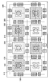
- FIG. 1 is a plan view showing an example of a planar layout of a pixel array provided in a solid-state imaging device according to the present embodiment.
- the planar layout of the pixel array 500 provided in the solid-state imaging device according to the present embodiment will be described.
- the pixel array 500 included in the solid-state imaging device according to the present embodiment is configured by arranging a plurality of pixels that respectively receive light of a predetermined wavelength band.
- the pixel array 500 is configured by arranging pixels (red pixels, green pixels and blue pixels) that respectively receive light in wavelength bands corresponding to red, green and blue in a predetermined array. It is also good.
- the pixel array 500 may be configured by repeatedly arranging pixel units in which four pixels of a red pixel, a blue pixel, and two green pixels form one set.
- the pixel array 500 may be configured by repeatedly arranging pixel units in which four pixels of red pixels, green pixels, blue pixels, and white pixels (that is, pixels without a color filter) are one set.
- the arrangement of the plurality of pixels in the pixel array 500 is not particularly limited. For example, various arrangements such as a delta arrangement, a stripe arrangement, a diagonal arrangement, or a rectangular arrangement can be applied.
- each of the pixels acquires distance measurement information for focus detection in addition to the pixel information for image generation.
- each of the pixels is configured by providing a pair of sub-pixels under one microlens in order to obtain distance measurement information for focus detection.
- a light flux incident from one side of the microlens is received by one sub-pixel, and a light flux incident from the other side of the microlens is received by the other sub-pixel.
- a shift amount (shift amount) that is correlated with the defocus amount of the focal point with respect to the subject is generated between the image received by one sub-pixel and the image received by the other sub-pixel.
- each of the pixels can detect the defocus amount of the focal point with respect to the subject by comparing the images received by each of the pair of sub-pixels with each other.
- the pixel array 500 includes the first pixel 100 in which the pair of sub pixels 110 and 120 are arranged in the first direction, and the pair of sub pixels 210 and 220. At least one or more second pixels 200 provided in line in a second direction orthogonal to one direction are included.
- the first pixel 100 includes a pair of sub pixels 110 and 120 and a pixel transistor group 150. Further, the second pixel 200 includes a pair of sub-pixels 210 and 220 and a pixel transistor group 250 similarly to the first pixel 100.
- the first pixel 100 and the second pixel 200 have substantially the same configuration except for the direction in which the pair of sub-pixels are arranged, and therefore, the first pixel 100 will be described below as an example.
- the pair of sub-pixels 110 and 120 are provided below the one microlens and the color filter in the first direction or the second direction, and ranging information for focus detection by photoelectrically converting incident light. And obtain pixel information for image generation.
- the sub pixels 110 and 120 can obtain information for focus detection by calculating the shift amount of the image received by each of the sub pixels 110 and 120.
- the sub-pixels 110 and 120 can acquire pixel information for obtaining a color image of a subject by performing signal processing on signals photoelectrically converted in each of the sub-pixels 110 and 120.
- the sub pixels 110 and 120 may be provided in the same planar shape. By providing the sub-pixels 110 and 120 with the same configuration except for the position with respect to the microlens, it is possible to accurately detect the amount of image shift due to pupil division. Specifically, the sub pixels 110 and 120 may be provided in the same planar shape so as to have the same aperture. For example, the planar shape of the sub pixels 110 and 120 may be a rectangular shape obtained by dividing a square into two.
- the pixel transistor group 150 generates information output from the first pixel 100 by transferring and amplifying signals output from the sub-pixels 110 and 120. Specifically, the pixel transistor group 150 may generate distance measurement information for focus detection and pixel information for image generation based on the signals output from the sub-pixels 110 and 120. For example, the pixel transistor group 150 may obtain pixel information for generating an image by adding up the signals output from each of the sub-pixels 110 and 120.
- each of the pixels of the pixel array 500 can obtain distance measurement information for focus detection and pixel information for image generation from the same pixel. Become.
- each of the pixels of the pixel array 500 acquires either information for focus detection or information for image generation, the more pixels for focus detection, the less pixels for acquiring pixel information. The image quality of the image is degraded. On the other hand, as the number of pixels for which focus detection is performed is reduced, the focusing accuracy is lowered, and the image tends to be blurred. That is, when each of the pixels of the pixel array 500 acquires either information for focus detection or information for image generation, the accuracy of focusing and the image quality of the image have a trade-off relationship. I will. On the other hand, according to the solid-state imaging device according to the present embodiment, it is possible to improve the focusing accuracy without degrading the image quality of the image.
- the directions in which the pair of sub-pixels are arranged are orthogonal to each other.
- the amount of shift in focus with respect to the object is calculated using the amount of shift generated between the image received by one sub-pixel and the image received by the other sub-pixel doing. Therefore, it may be difficult to detect an accurate defocus amount for an object having a shape that does not easily generate a displacement amount between each of the pair of sub-pixels. For example, in the case where the subject has an elongated shape extending in a direction orthogonal to the direction in which the pair of sub-pixels is arranged, an accurate defocus amount is detected only with the pixel in which the pair of sub-pixels is arranged in one direction. Can be difficult.
- the shape of the object is elongated in any direction Even with the shape, it is possible to detect an accurate defocus amount.
- the pixel array 500 even if the shape of the subject is elongated in any direction, an accurate defocus amount is detected in either the first pixel 100 or the second pixel 200. Is possible. Therefore, according to the solid-state imaging device according to the present embodiment, it is possible to perform focus detection and image generation on subjects of various shapes, and thus it is possible to obtain a clearer image.
- the planar shape of the first pixel 100 and the second pixel 200 may be a four-fold symmetric planar shape.
- the planar shapes of the first pixel 100 and the second pixel 200 may be shapes that coincide with each other by rotating 90 ° around the center of gravity.
- the planar shape of the first pixel 100 and the second pixel 200 is four-fold symmetric, the second pixel 200 can be formed by rotating the first pixel 100 by 90 °.
- the two pixels 200 can be more easily mixed and formed.
- a four-fold symmetrical shape for example, a square, regular octagon or circular shape can be exemplified.
- the first pixel 100 and the second pixel 200 may have the same planar shape. In such a case, it is easy to spread the first pixel 100 and the second pixel 200 in the pixel array 500. Further, in such a case, since the aperture ratio of the pixel is the same in each of the first pixel 100 and the second pixel 200, it may be used for image generation without correcting the pixel information acquired from each pixel. it can.
- the pixel array 500 may include pixels having at least one or more pairs of sub-pixels for obtaining distance measurement information for focusing as described above and pixel information for image generation. That is, the pixel array 500 may include at least one or more of the first pixel 100 and the second pixel 200 described above. In such a case, the green pixel may be the first pixel 100 and the second pixel 200 including a pair of sub-pixels.
- the green light photoelectrically converted by the green pixel is more easily absorbed by the silicon photodiode than the red light and blue light photoelectrically converted by the red pixel and the blue pixel, so it is easily photoelectrically converted and a signal is easily obtained. Therefore, when the first pixel 100 and the second pixel 200 are green pixels, it is possible to obtain distance measurement information for focus detection with higher accuracy.
- FIG. 2 is a longitudinal sectional view showing the configuration of one sub-pixel in FIG.
- the sub-pixels constituting the first pixel 100 and the second pixel 200 and the like are configured by the photoelectric conversion element 11 embedded in the semiconductor substrate 50, the transfer transistor 12, and the floating diffusion layer 13. Be done.
- the pixel control transistor 14 is, for example, one of the transistors included in the transistor group shown as the pixel transistor group 150 in FIG.
- the semiconductor substrate 50 is a substrate formed of a semiconductor material.
- the semiconductor substrate 50 may be a silicon substrate.
- the semiconductor substrate 50 is a substrate formed of another elemental semiconductor such as germanium or a substrate formed of a compound semiconductor such as gallium arsenide (GaAs), gallium nitride (GaN) or silicon carbide (SiC). It is also good.
- GaAs gallium arsenide
- GaN gallium nitride
- SiC silicon carbide
- the photoelectric conversion element 11 is, for example, a photodiode, and is embedded in the semiconductor substrate 50 and provided. Specifically, the photoelectric conversion element 11 converts light incident on the sub-pixel into electrons and holes by the photovoltaic effect by the pn junction or the pin junction.
- the photoelectric conversion element 11 may be configured by an n-type semiconductor region provided inside a p-type semiconductor region. In the photoelectric conversion element 11, when light is incident, electrons are generated in the n-type semiconductor region, and holes are generated in the p-type semiconductor region.
- the sub-pixel can convert the light incident on the sub-pixel into a signal by extracting the electrons generated in the n-type semiconductor region by the transfer transistor 12.
- the transfer transistor 12 takes out the charge from the photoelectric conversion element 11 provided inside the semiconductor substrate 50 and transfers the taken out charge to the floating diffusion layer 13 on the surface of the semiconductor substrate 50.
- the transfer transistor 12 is provided as a vertical transistor having a vertical gate structure extending toward the inside of the semiconductor substrate 50, and causes the photoelectric conversion element 11 and the floating diffusion layer 13 to function as a source or drain region. . Therefore, when a voltage higher than the threshold voltage is applied to the vertical gate, the transfer transistor 12 forms a channel along the vertical gate, thereby floating the charge generated in the photoelectric conversion element 11 into the floating diffusion layer 13. Can be transferred to
- the floating diffusion layer 13 is formed as an n-type semiconductor region and stores charge.
- the floating diffusion layer 13 functions as a floating diffusion.
- the floating diffusion layer 13 controls, for example, the gate voltage of the amplification transistor by the potential generated by the accumulated charge, and reads out the signal generated by the light reception of the sub-pixel to the outside of the pixel.
- the pixel control transistor 14 is a field effect transistor provided on the surface of the semiconductor substrate 50.
- the pixel control transistor 14 includes a gate electrode provided on the semiconductor substrate 50 and a source or drain region provided on the semiconductor substrate 50 with the gate electrode interposed therebetween.
- the pixel control transistor 14 may be provided in a region overlapping with the photoelectric conversion element 11 when the main surface of the semiconductor substrate 50 is viewed in plan.
- the photoelectric conversion element 11 is embedded in the semiconductor substrate 50, and the distance from the surface of the semiconductor substrate 50 is large. According to this configuration, it is possible to superimpose the pixel control transistor 14 that is easily affected by noise or the like on the photoelectric conversion element 11 when the pixel control transistor 11 approaches the photoelectric conversion element 11.
- the photoelectric conversion element 11 and the pixel control transistor 14 can be formed so as to be superimposed on the same planar region, so that the volume of the photoelectric conversion element 11 can be increased.
- the sub-pixel can reduce the area of the entire sub-pixel without reducing the sensitivity, the amount of saturated electrons, and the like of the photoelectric conversion element 11.
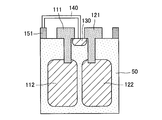
- FIG. 3A is a plan view showing a plan configuration of one pixel of the solid-state imaging device according to the present embodiment
- FIG. 3B is a longitudinal sectional view schematically showing a cross section cut along line A-AA in FIG. 3A.
- FIG. 3C is a circuit diagram showing an equivalent circuit of the configuration shown in FIG. 3A.
- the first pixel 100 is described as an example, the second pixel 200 is the same except that the arrangement direction of the pair of sub-pixels is different.
- the first pixel 100 includes a pair of sub-pixels 110 and 120, vertical gate electrodes 111 and 121, a floating diffusion layer 130, a pixel wiring 140, and an amplification transistor 151.
- a selection transistor 152, a reset transistor 153, and a dummy gate 154 are provided.
- photoelectric conversion elements 112 and 122 are provided in the semiconductor substrate 50 in the regions corresponding to the sub-pixels 110 and 120, respectively.
- the pair of sub pixels 110 and 120 includes a pair of photoelectric conversion elements 112 and 122 formed inside the semiconductor substrate 50, and converts the received light into a charge.
- the pair of sub-pixels 110 and 120 correspond to a pair of photoelectric conversion elements 112 and 122
- the photoelectric conversion elements 112 and 122 are a pair of n-type semiconductor regions provided inside a p-type semiconductor region. It consists of In the photoelectric conversion elements 112 and 122, the incident light is converted into charges by the photovoltaic effect. Specifically, electrons are generated in the n-type semiconductor region, and holes are generated in the p-type semiconductor region.
- the photoelectric conversion elements 112 and 122 can convert the amount of incident light into the amount of electrons generated in the n-type semiconductor region. Note that since the photoelectric conversion elements 112 and 122 are p-type semiconductor regions between n-type semiconductor regions, they are electrically separated from each other by potential barriers.
- the photoelectric conversion elements 112 and 122 can be increased in volume by being provided inside the semiconductor substrate 50, so that the sensitivity, the amount of saturated electrons, and the like can be increased without increasing the planar occupied area. it can.
- the semiconductor substrate 50 may be a substrate formed of a semiconductor material such as silicon, a substrate formed of another elemental semiconductor such as germanium, or gallium arsenide (GaAs), gallium nitride (GaN), or silicon carbide It may be a substrate formed of a compound semiconductor such as SiC).
- the vertical gate electrodes 111 and 121 are gates of field effect transistors that transfer the charges generated by the photoelectric conversion elements 112 and 122 to the floating diffusion layer 130, respectively.
- the vertical gate electrodes 111 and 121 are provided in the form of vertically elongated columns extending inside the semiconductor substrate 50 in order to extract charges from the photoelectric conversion elements 112 and 122 provided inside the semiconductor substrate 50.
- the vertical gate electrodes 111 and 121 form a channel between the photoelectric conversion elements 112 and 122 and the floating diffusion layer 130 along the vertical gate electrodes 111 and 121, respectively using the source and drain regions.
- the vertical gate electrodes 111 and 121 can transfer charges from the photoelectric conversion elements 112 and 122 to the floating diffusion layer 130 through the formed channel.
- the floating diffusion layer 130 is formed as an n-type semiconductor region, and stores charge.
- the floating diffusion layer 130 functions as a floating diffusion.
- the charge transferred from the photoelectric conversion elements 112 and 122 and accumulated in the floating diffusion layer 130 generates a potential to control the gate voltage of the amplification transistor 151 via the pixel wiring 140.
- the floating diffusion layer 130 may be provided, for example, at the boundary between the pair of sub-pixels 110 and 120 (that is, the photoelectric conversion elements 112 and 122). More specifically, the floating diffusion layer 130 may be provided at the center of the first pixel 100 configured by the pair of sub-pixels 110 and 120. In such a case, the center of the floating diffusion layer 130 can be substantially aligned with the center of the microlens provided on the first pixel 100.
- the pixel wiring 140 is a wiring and a contact which electrically connect the floating diffusion layer 130 and the gate electrode of the amplification transistor 151 and electrically connect the floating diffusion layer 130 and the source or drain region of the reset transistor 153.
- the pixel line 140 may be formed of a metal such as copper (Cu), aluminum (Al), titanium (Ti), or tungsten (W).
- the pixel wiring 140 may be formed of one type of metal or may be formed of a plurality of types of metals. For example, the pixel wiring 140 may be formed of a different metal for each wiring and contact.
- the gate electrode of the amplification transistor 151 is electrically connected to the floating diffusion layer 130 by the pixel wiring 140, and on / off is controlled by the potential generated by the charge accumulated in the floating diffusion layer 130. Specifically, when the potential generated by the charge accumulated in the floating diffusion layer 130 exceeds the threshold, the amplification transistor 151 is turned on to cause a current to flow between the source and the drain. Thereby, the amplification transistor 151 can convert and amplify the charge stored in the floating diffusion layer 130 into the current between the source and the drain.
- the selection transistor 152 is connected in series to the amplification transistor 151, and controls selection or non-selection of a pixel. Specifically, the selection transistor 152 controls whether or not the signal is read from the first pixel 100 by the voltage applied to the gate electrode. Thereby, in the solid-state imaging device, signals can be read out sequentially from each of the pixels.
- the source or drain region and the floating diffusion layer 130 are electrically connected by the pixel wiring 140, and the potential of the floating diffusion layer 130 is controlled.
- the source or drain of the reset transistor 153 is connected to, for example, a power supply (VDD).
- the reset transistor 153 is turned on to form a channel between the source and the drain, and controls the potential of the floating diffusion layer 130 to be equal to the potential of the power supply (VDD).
- the dummy gate 154 is an electrode which is not electrically connected to the wiring for exchanging signals and the like but is electrically connected to the ground. That is, the dummy gate 154 is an electrode that is not used for signal processing of the signal output from the first pixel 100.
- the dummy gate 154 is provided to make the arrangement of gate electrodes provided around the pair of sub-pixels 110 and 120 of the first pixel 100 symmetrical with respect to the sub-pixels 110 and 120.
- the dummy gate 154 is provided so that light reflected by each gate electrode of the amplification transistor 151, the selection transistor 152, and the reset transistor 153 leaks symmetrically to the photoelectric conversion elements 112 and 122.
- the amplification transistor 151, the selection transistor 152, the reset transistor 153, and the dummy gate 154 are formed along two sides of the first pixel 100 configured by a pair of sub pixels 110 and 120. On the remaining two sides of the first pixel 100, any of the amplification transistor 151, the selection transistor 152, the reset transistor 153, and the dummy gate 154 of the adjacent pixel may be formed.
- FIG. 3C An equivalent circuit of the circuit of the first pixel 100 described above is shown in FIG. 3C.
- the photoelectric conversion elements 112 and 122 are connected to the gate of the amplification transistor 151 via the floating diffusion layer 130.
- the floating diffusion layer 130 is connected to the power supply (VDD) through the source or drain of the reset transistor 153.
- the amplification transistor 151 is connected in series to the selection transistor 152, the source or drain of the amplification transistor 151 is connected to the power supply (VDD), and the source or drain of the selection transistor 152 is connected to the output (VOUT).
- the charge photoelectrically converted by the photoelectric conversion elements 112 and 122 is output to the floating diffusion layer 130 by the potential difference between the ground and the VDD.
- the output charge is accumulated in the floating diffusion layer 130 to increase the voltage applied to the gate of the amplification transistor 151, thereby turning on the amplification transistor 151.
- the selection transistor 152 is turned on to form an electrical connection from the power supply (VDD) to the output (VOUT).
- VDD power supply
- VOUT output
- the reset transistor 153 is turned on to discharge the charge stored in the floating diffusion layer 130, and the potential of the floating diffusion layer 130 is reset to the potential of the power supply (VDD). It is set. Thus, the floating diffusion layer 130 returns to the state before the charge photoelectrically converted by the photoelectric conversion elements 112 and 122 is accumulated.
- FIG. 3D is a plan view showing a planar configuration of the wiring for each of the first pixel 100 and the second pixel 200.
- FIG. 3D shows a specific example of the wiring connection in the case where the first pixel 100 and the second pixel 200 are adjacent to each other.
- the second pixel 200 has substantially the same configuration as the first pixel 100 except that the arrangement direction of the pair of sub-pixels 210 and 220 is different.
- the second pixel 200 includes a pair of sub-pixels 210 and 220, vertical gate electrodes 211 and 221, a floating diffusion layer 230, a pixel wiring 240, an amplification transistor 251, and a selection transistor 252, A reset transistor 253 and a dummy gate 254 are provided. These configurations are substantially the same as the configurations of the same name described in the first pixel 100.
- the pixel wiring 140 is provided in a shape bent in a bowl shape.
- the pixel wiring 140 is electrically connected to the floating diffusion layer 130 by the contact 163 provided at the apex of the wedge shape, and electrically connected to the gate electrode of the amplification transistor 151 by the contact 162 provided at one end of the wedge shape.
- the pixel wiring 240 is provided in a wedge shape.
- the pixel wiring 240 is electrically connected to the floating diffusion layer 230 at the contact 263 provided at the apex of the wedge, and electrically connected to the gate electrode of the amplification transistor 251 at the contact 262 provided at one end of the wedge. Connecting.
- gate wirings 141 and 142 for controlling on / off of transfer transistors that control transfer of charges from each of the pair of sub-pixels 110 and 120 are provided in the form of parallel line segments.
- the gate wiring 141 is electrically connected to the vertical gate electrode 111 at the contact 161
- the gate wiring 142 is electrically connected to the vertical gate electrode 121 at the contact 164.
- the contact 161 and the contact 164 are provided to be located on the diagonal of the first pixel 100, respectively. Since the gate wirings 141 and 142 are provided in the same layer as the pixel wiring 140, they are provided so as not to overlap with each other.
- the pixel wiring 140 is provided on the third quadrant side of the first pixel 100
- the gate wiring 141 is provided on the first quadrant and the second quadrant side
- the gate wiring 142 is provided on the fourth quadrant side.
- the gate wirings 141 and 142 are electrically connected to the interpixel wirings 310 and 320 provided in the upper layer by the vias 171 and 172, respectively.
- gate wirings 241 and 242 for controlling on / off of transfer transistors for controlling transfer of charges from each of the pair of sub-pixels 210 and 220 are provided in the form of parallel line segments.
- the gate wiring 241 is electrically connected to the vertical gate electrode 211 at the contact 261
- the gate wiring 242 is electrically connected to the vertical gate electrode 221 at the contact 264.
- the contact 261 and the contact 264 are provided on the diagonal of the second pixel 200, respectively. Since the gate wirings 241 and 242 are provided in the same layer as the pixel wiring 240, they are provided so as not to overlap with each other.
- the pixel wiring 240 is provided on the third quadrant side of the second pixel 200
- the gate wiring 241 is provided on the first quadrant and the second quadrant side
- the gate wiring 242 is provided on the fourth quadrant side.
- the gate wirings 241 and 242 are electrically connected to the interpixel wirings 310 and 320 provided in the upper layer by the vias 271 and 272, respectively.
- the arrangement direction of the pair of sub-pixels is orthogonal.
- the first pixel 100 and the second pixel 200 have the same wiring shape by providing contacts for the vertical gate electrodes provided in each of the pair of sub-pixels on the diagonal of each pixel. Can be connected.
- the pixel wiring 140 and the gate wirings 141 and 142, and the pixel wiring 240 and the gate wirings 241 and 242 can be provided in the same shape.
- the inter-pixel wirings 310 and 320 provided over the first pixel 100 and the second pixel 200 can be provided in a linear shape extending in one direction.
- the first pixel 100 and the second pixel 200 are provided with the wiring of the same shape, there is no difference in the conversion efficiency with respect to the parasitic capacitance. Further, even when the arrangement of the first pixel 100 and the second pixel 200 is changed, it is possible to cope with the case without changing the wiring only by changing the configuration of the transistor of the semiconductor substrate 50.
- FIG. 4 is a longitudinal sectional view showing a modification of the configuration of one sub-pixel.
- the sub-pixels constituting the first pixel 100, the second pixel 200, etc. are formed of the photoelectric conversion element 11 embedded in the semiconductor substrate 50, the extraction region 16, the transfer transistor 15, and the floating diffusion layer. 13 and the pixel control transistor 14.
- the transfer transistor 15 does not have a vertical gate structure, but has a planar gate structure in which a gate is provided on the surface of a semiconductor substrate 50.
- a lead-out area 16 extending from the photoelectric conversion element 11 toward the surface of the semiconductor substrate 50 is provided.
- description here is abbreviate
- the lead-out area 16 is an n-type semiconductor area, and the electrons generated in the n-type semiconductor area of the photoelectric conversion element 11 are drawn to the surface of the semiconductor substrate 50.
- the transfer transistor 15 can function as a gate the electrode provided on the surface of the semiconductor substrate 50, and can function the extraction region 16 and the floating diffusion layer 13 as a source or drain region. That is, in the transfer transistor 15, when a voltage higher than the threshold voltage is applied to the gate electrode provided on the surface of the semiconductor substrate 50, the channel between the floating region 13 and the extraction region 16 near the surface of the semiconductor substrate 50. Can be formed.
- the transfer transistor 15 can transfer the electrons generated by the photoelectric conversion element 11 to the floating diffusion layer 13 through the lead-out region 16.
- FIG. 5A is a plan view showing a modification of a planar configuration including a plurality of pixels
- FIG. 5B is a circuit diagram showing an equivalent circuit of the configuration shown in FIG. 5A.
- the floating diffusion layers 131 and 132 of two pixels are electrically connected by the pixel wiring 140, so that the pixel transistor group 150 after the amplification transistor is shared by two pixels. doing.
- the floating diffusion layer 131 which accumulates the charge photoelectrically converted in the pair of sub-pixels 110A and 120A of the first pixel 101, and the pair of sub-pixels 110B and 120B of the first pixel 102.
- the pixel wiring 140 electrically connects to the floating diffusion layer 132 which stores the photoelectrically converted charge.
- the floating diffusion layer 131, the floating diffusion layer 132, and the pixel wiring 140 are at the same potential, so that the entire floating diffusion layer 131, the floating diffusion layer 132, and the pixel wiring 140 can function as one floating diffusion.
- the first pixels 101 and 102 can share the pixel transistor group 150 (that is, the amplification transistor, the selection transistor, and the reset transistor) constituting the circuit of the latter stage of the floating diffusion by two pixels,
- the area occupied by the signal processing circuit can be reduced, and the area occupied by the pixel can be expanded.
- the photoelectric conversion is performed by the floating diffusion layer 133 that accumulates the charge photoelectrically converted by the pair of sub-pixels 110C and 120C of the first pixel 103 and the pair of sub-pixels 210 and 220 of the second pixel 201
- the pixel wiring 240 electrically connects the floating diffusion layer 230 for storing the charge.
- the floating diffusion layer 133, the floating diffusion layer 230, and the pixel wiring 240 are at the same potential, so that the entire floating diffusion layer 133, the floating diffusion layer 230, and the pixel wiring 140 can function as one floating diffusion.
- the first pixel 103 and the second pixel 201 can share the pixel transistor group 250 (that is, the amplification transistor, the selection transistor, and the reset transistor) constituting the circuit of the latter stage of the floating diffusion by two pixels. Therefore, the area occupied by the signal processing circuit can be reduced, and the area occupied by the pixel can be expanded.
- the pixel transistor group 250 that is, the amplification transistor, the selection transistor, and the reset transistor
- FIG. 5B An equivalent circuit of the circuit of the first pixels 101 and 102 sharing the signal processing circuit described in FIG. 5A is shown in FIG. 5B.
- the floating diffusion layers 131 and 132 and the pixel wiring 140 function as floating diffusions and are connected to the gate of the amplification transistor 151.
- the floating diffusion is connected to the power supply (VDD) through the source or drain of the reset transistor 153.
- the amplification transistor 151 is connected in series to the selection transistor 152, the source or drain of the amplification transistor 151 is connected to the power supply (VDD), and the source or drain of the selection transistor 152 is connected to the output (VOUT) There is.
- the charges photoelectrically converted in each of the sub-pixels 110A, 120A, 110B, and 120B are output to the floating diffusion layers 131 and 132 by the potential difference between the ground and the VDD.
- the output charge is accumulated across the floating diffusion layers 131 and 132 and the pixel wiring 140 to increase the voltage applied to the gate of the amplification transistor 151, thereby turning on the amplification transistor 151.
- the selection transistor 152 is turned on to form an electrical connection from the power supply (VDD) to the output (VOUT).
- VDD power supply
- VOUT output
- the reset transistor 153 is turned on, whereby the charges accumulated over the floating diffusion layers 131 and 132 and the pixel wiring 140 are discharged, and the potential of the floating diffusion layers 131 and 132 Is reset to the potential of the power supply (VDD). Thereby, the floating diffusion layers 131 and 132 return to the state before the charge is accumulated.
- FIG. 6 is a plan view showing a modification of the plane configuration including a plurality of pixels.
- the floating diffusion layer 130 is provided at the boundary between two pixels, so that the pixel transistor group 150 constituting the circuit of the subsequent stage of the floating diffusion layer 130 is shared by two pixels. ing.
- the charge photoelectrically converted in the pair of sub-pixels 110A and 120A of the first pixel 101 and the charge photoelectrically converted in the pair of sub-pixels 110B and 120B of the first pixel 102 are the first It is accumulated in the floating diffusion layer 130 provided at the boundary between the pixels 101 and 102.
- the floating diffusion layer 130 is electrically connected to the pixel transistor group 150 including the amplification transistor and the reset transistor by the pixel wiring 140. According to this, since the first pixels 101 and 102 can share the floating diffusion layer 130 and the pixel transistor group 150 (that is, the amplification transistor, the selection transistor, and the reset transistor) by two pixels, the signal processing circuit The area occupied can be reduced, and the area occupied by the pixel can be enlarged.
- the charge photoelectrically converted by the pair of sub-pixels 210A and 220A of the second pixel 201 and the charge photoelectrically converted by the pair of sub-pixels 210B and 220B of the second pixel 202 are the second It is accumulated in the floating diffusion layer 230 provided at the boundary between the pixels 201 and 202.
- the floating diffusion layer 230 is electrically connected to the pixel transistor group 250 including the amplification transistor and the reset transistor by the pixel wiring 240.
- the second pixels 201 and 202 can share the floating diffusion layer 230 and the pixel transistor group 250 (that is, the amplification transistor, the selection transistor, and the reset transistor) by two pixels, the signal processing circuit The area occupied can be reduced, and the area occupied by the pixel can be enlarged.
- FIG. 7 is a plan view showing a modification of the plane configuration of the pixel array 500. As shown in FIG.
- the pixel array 500 may be provided to be inclined with respect to the solid-state imaging device. Specifically, the pixel array 500 may be provided to be inclined 45 ° with respect to the horizontal direction of the solid-state imaging device.
- the pair of sub-pixels 110 and 120 of the first pixel 100 are arranged in a direction inclined 45 ° clockwise, for example, with respect to the horizontal direction of the solid-state imaging device.
- the pair of sub-pixels 110 and 120 of the second pixel 200 are arranged in a direction inclined 45 ° counterclockwise, for example, with respect to the horizontal direction of the solid-state imaging device.
- the pixel array 500 provided in the solid-state imaging device according to the present embodiment may have another planar configuration other than the planar configuration in which each of the pixels is arranged in a matrix.
- FIG. 8 is a plan view showing a modification of the planar configuration of the pixel array 500. As shown in FIG.
- the pixel array 500 may be provided at an angle to the solid-state imaging device. Specifically, the pixel array 500 may be provided to be inclined 45 ° with respect to the horizontal direction of the solid-state imaging device.
- the pair of sub-pixels 110 and 120 of the first pixel 100 are provided to be arranged in the vertical direction with respect to the horizontal direction of the solid-state imaging device.
- the sub-pixels 110 and 120 are arranged in the horizontal direction of the solid-state imaging device.
- the planar shape of the pair of sub-pixels of each pixel may be, for example, a right-angled isosceles triangle obtained by cutting a square with a diagonal.
- the shape of the pair of sub-pixels may be another shape other than a rectangle obtained by equally dividing a square into two.
- the first to fifth modifications described above can be combined with one another as long as no contradiction arises, and these are also included in the technical scope of the present disclosure.
- a plurality of types of plane configurations according to the second to fifth modifications may be included in the same pixel array 500.
- the solid-state imaging device according to an embodiment of the present disclosure can be applied to, for example, an imaging unit mounted in various electronic devices. Subsequently, examples of electronic devices to which the solid-state imaging device according to the present embodiment can be applied will be described with reference to FIGS. 9A to 9C.
- 9A to 9C are external views showing an example of an electronic apparatus to which the solid-state imaging device according to the present embodiment can be applied.
- the solid-state imaging device according to the present embodiment can be applied to an imaging unit mounted in an electronic device such as a smartphone.
- the smartphone 900 includes a display unit 901 for displaying various information, and an operation unit 903 configured of a button or the like for receiving an operation input by the user.
- the solid-state imaging device according to the present embodiment may be applied to the imaging unit included in the smartphone 900.
- the solid-state imaging device can be applied to an imaging unit mounted in an electronic device such as a digital camera.
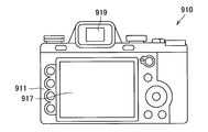
- the digital camera 910 includes a main body (camera body) 911, an interchangeable lens unit 913, a grip 915 gripped by the user at the time of photographing, A monitor unit 917 for displaying information and an EVF (Electronic View Finder) 919 for displaying a through image observed by the user at the time of shooting are provided.
- 9B is an external view of the digital camera 910 as viewed from the front (ie, the object side)
- FIG. 9C is an external view of the digital camera 910 as viewed from the rear (ie, the photographer side).
- the solid-state imaging device may be applied to the imaging unit of the digital camera 910.
- the electronic device to which the solid-state imaging device according to the present embodiment is applied is not limited to the above example.
- the solid-state imaging device according to the present embodiment can be applied to an imaging unit mounted in an electronic device in any field.
- an electronic device for example, a glasses-type wearable device, an HMD (Head Mounted Display), a television device, an electronic book, a PDA (Personal Digital Assistant), a notebook personal computer, a video camera, a game device, etc. are illustrated. be able to.
- FIG. 10 is a diagram showing an example of a schematic configuration of an endoscopic surgery system to which the technology (the present technology) according to the present disclosure can be applied.
- FIG. 10 illustrates how a surgeon (doctor) 11131 is performing surgery on a patient 11132 on a patient bed 11133 using the endoscopic surgery system 11000.
- the endoscopic surgery system 11000 includes an endoscope 11100, other surgical instruments 11110 such as an insufflation tube 11111 and an energy treatment instrument 11112, and a support arm device 11120 for supporting the endoscope 11100.
- a cart 11200 on which various devices for endoscopic surgery are mounted.
- the endoscope 11100 includes a lens barrel 11101 whose region of a predetermined length from the tip is inserted into a body cavity of a patient 11132, and a camera head 11102 connected to a proximal end of the lens barrel 11101.
- the endoscope 11100 configured as a so-called rigid endoscope having a rigid barrel 11101 is illustrated, but even if the endoscope 11100 is configured as a so-called flexible mirror having a flexible barrel Good.
- the endoscope 11100 may be a straight endoscope, or may be a oblique endoscope or a side endoscope.
- An optical system and an imaging device are provided inside the camera head 11102, and the reflected light (observation light) from the observation target is condensed on the imaging device by the optical system.
- the observation light is photoelectrically converted by the imaging element to generate an electric signal corresponding to the observation light, that is, an image signal corresponding to the observation image.
- the image signal is transmitted as RAW data to a camera control unit (CCU: Camera Control Unit) 11201.
- CCU Camera Control Unit
- the CCU 11201 is a CPU (Central Processing Unit) or a GPU (Graphics). (Processing Unit) etc., and controls the operation of the endoscope 11100 and the display device 11202 in a centralized manner. Furthermore, the CCU 11201 receives an image signal from the camera head 11102 and performs various image processing for displaying an image based on the image signal, such as development processing (demosaicing processing), on the image signal.
- image processing demosaicing processing
- the display device 11202 displays an image based on an image signal subjected to image processing by the CCU 11201 under control of the CCU 11201.
- the light source device 11203 includes, for example, a light source such as an LED (light emitting diode), and supplies the endoscope 11100 with irradiation light at the time of imaging an operation part or the like.
- a light source such as an LED (light emitting diode)
- the input device 11204 is an input interface to the endoscopic surgery system 11000.
- the user can input various information and input instructions to the endoscopic surgery system 11000 via the input device 11204.
- the user inputs an instruction to change the imaging condition (type of irradiated light, magnification, focal length, and the like) by the endoscope 11100, and the like.
- the treatment tool control device 11205 controls the drive of the energy treatment tool 11112 for ablation of tissue, incision, sealing of a blood vessel, and the like.
- the insufflation apparatus 11206 is a gas within the body cavity via the insufflation tube 11111 in order to expand the body cavity of the patient 11132 for the purpose of securing a visual field by the endoscope 11100 and securing a working space of the operator.
- Send The recorder 11207 is a device capable of recording various types of information regarding surgery.
- the printer 11208 is an apparatus capable of printing various types of information regarding surgery in various types such as text, images, and graphs.
- the light source device 11203 that supplies the irradiation light when imaging the surgical site to the endoscope 11100 can be configured of, for example, an LED, a laser light source, or a white light source configured by a combination of these.
- a white light source is configured by a combination of RGB laser light sources
- the output intensity and output timing of each color (each wavelength) can be controlled with high precision. It can be carried out.
- the laser light from each of the RGB laser light sources is irradiated to the observation target in time division, and the drive of the image pickup element of the camera head 11102 is controlled in synchronization with the irradiation timing to cope with each of RGB. It is also possible to capture a shot image in time division. According to the method, a color image can be obtained without providing a color filter in the imaging device.
- the drive of the light source device 11203 may be controlled so as to change the intensity of the light to be output every predetermined time.
- the drive of the imaging device of the camera head 11102 is controlled in synchronization with the timing of the change of the light intensity to acquire images in time division, and by combining the images, high dynamic without so-called blackout and whiteout is obtained. An image of the range can be generated.
- the light source device 11203 may be configured to be able to supply light of a predetermined wavelength band corresponding to special light observation.
- special light observation for example, the mucous membrane surface layer is irradiated by irradiating narrow band light as compared with irradiation light (that is, white light) at the time of normal observation using the wavelength dependency of light absorption in body tissue.
- the so-called narrow band imaging is performed to image a predetermined tissue such as a blood vessel with high contrast.
- fluorescence observation may be performed in which an image is obtained by fluorescence generated by irradiation with excitation light.
- body tissue is irradiated with excitation light and fluorescence from the body tissue is observed (autofluorescence observation), or a reagent such as indocyanine green (ICG) is locally injected into body tissue and the body tissue is Excitation light corresponding to the fluorescence wavelength of the reagent can be irradiated to obtain a fluorescence image or the like.
- the light source device 11203 can be configured to be able to supply narrow band light and / or excitation light corresponding to such special light observation.
- FIG. 11 is a block diagram showing an example of functional configurations of the camera head 11102 and the CCU 11201 shown in FIG.
- the camera head 11102 includes a lens unit 11401, an imaging unit 11402, a drive unit 11403, a communication unit 11404, and a camera head control unit 11405.
- the CCU 11201 includes a communication unit 11411, an image processing unit 11412, and a control unit 11413.
- the camera head 11102 and the CCU 11201 are communicably connected to each other by a transmission cable 11400.
- the lens unit 11401 is an optical system provided at a connection portion with the lens barrel 11101.
- the observation light taken in from the tip of the lens barrel 11101 is guided to the camera head 11102 and is incident on the lens unit 11401.
- the lens unit 11401 is configured by combining a plurality of lenses including a zoom lens and a focus lens.
- the imaging device constituting the imaging unit 11402 may be one (a so-called single-plate type) or a plurality (a so-called multi-plate type).
- the imaging unit 11402 When the imaging unit 11402 is configured as a multi-plate type, for example, an image signal corresponding to each of RGB may be generated by each imaging element, and a color image may be obtained by combining them.
- the imaging unit 11402 may be configured to have a pair of imaging devices for acquiring image signals for right eye and left eye corresponding to 3D (dimensional) display. By performing 3D display, the operator 11131 can more accurately grasp the depth of the living tissue in the operation site.
- a plurality of lens units 11401 may be provided corresponding to each imaging element.
- the imaging unit 11402 may not necessarily be provided in the camera head 11102.
- the imaging unit 11402 may be provided inside the lens barrel 11101 immediately after the objective lens.
- the driving unit 11403 is configured by an actuator, and moves the zoom lens and the focusing lens of the lens unit 11401 by a predetermined distance along the optical axis under the control of the camera head control unit 11405. Thereby, the magnification and the focus of the captured image by the imaging unit 11402 can be appropriately adjusted.
- the communication unit 11404 is configured of a communication device for transmitting and receiving various types of information to and from the CCU 11201.
- the communication unit 11404 transmits the image signal obtained from the imaging unit 11402 to the CCU 11201 as RAW data via the transmission cable 11400.
- the communication unit 11404 also receives a control signal for controlling the drive of the camera head 11102 from the CCU 11201 and supplies the control signal to the camera head control unit 11405.
- the control signal includes, for example, information indicating that the frame rate of the captured image is designated, information indicating that the exposure value at the time of imaging is designated, and / or information indicating that the magnification and focus of the captured image are designated, etc. Contains information about the condition.
- the imaging conditions such as the frame rate, exposure value, magnification, and focus described above may be appropriately designated by the user, or may be automatically set by the control unit 11413 of the CCU 11201 based on the acquired image signal. Good. In the latter case, the so-called AE (Auto Exposure) function, AF (Auto Focus) function, and AWB (Auto White Balance) function are incorporated in the endoscope 11100.
- AE Auto Exposure
- AF Auto Focus
- AWB Automatic White Balance
- the camera head control unit 11405 controls the drive of the camera head 11102 based on the control signal from the CCU 11201 received via the communication unit 11404.
- the communication unit 11411 is configured by a communication device for transmitting and receiving various types of information to and from the camera head 11102.
- the communication unit 11411 receives an image signal transmitted from the camera head 11102 via the transmission cable 11400.
- the communication unit 11411 transmits a control signal for controlling driving of the camera head 11102 to the camera head 11102.
- the image signal and the control signal can be transmitted by telecommunication or optical communication.
- An image processing unit 11412 performs various types of image processing on an image signal that is RAW data transmitted from the camera head 11102.
- the control unit 11413 performs various types of control regarding imaging of a surgical site and the like by the endoscope 11100 and display of a captured image obtained by imaging of the surgical site and the like. For example, the control unit 11413 generates a control signal for controlling the drive of the camera head 11102.
- control unit 11413 causes the display device 11202 to display a captured image in which a surgical site or the like is captured, based on the image signal subjected to the image processing by the image processing unit 11412.
- the control unit 11413 may recognize various objects in the captured image using various image recognition techniques. For example, the control unit 11413 detects a shape, a color, and the like of an edge of an object included in a captured image, thereby enabling a surgical tool such as forceps, a specific biological site, bleeding, mist when using the energy treatment tool 11112, and the like. It can be recognized.
- control unit 11413 may superimpose various surgical support information on the image of the surgery section using the recognition result.
- the operation support information is superimposed and presented to the operator 11131, whereby the burden on the operator 11131 can be reduced and the operator 11131 can reliably proceed with the operation.
- a transmission cable 11400 connecting the camera head 11102 and the CCU 11201 is an electric signal cable corresponding to communication of an electric signal, an optical fiber corresponding to optical communication, or a composite cable of these.
- communication is performed by wire communication using the transmission cable 11400, but communication between the camera head 11102 and the CCU 11201 may be performed wirelessly.
- the technology according to the present disclosure may be applied to, for example, the endoscope 11100 or the camera head 11102 among the configurations described above.
- the solid-state imaging device according to the present embodiment can be applied to the endoscope 11100 or the imaging unit 11402 of the camera head 11102.
- the technology according to the present disclosure may be applied to an in-vivo information acquisition system.
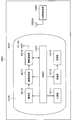
- FIG. 12 is a block diagram showing an example of a schematic configuration of a patient's in-vivo information acquiring system using a capsule endoscope to which the technology (the present technology) according to the present disclosure can be applied.
- the in-vivo information acquisition system 10001 includes a capsule endoscope 10100 and an external control device 10200.
- the capsule endoscope 10100 is swallowed by the patient at the time of examination.
- the capsule endoscope 10100 has an imaging function and a wireless communication function, and moves inside the organ such as the stomach and intestine by peristaltic movement and the like while being naturally discharged from the patient, Images (hereinafter, also referred to as in-vivo images) are sequentially captured at predetermined intervals, and information on the in-vivo images is sequentially wirelessly transmitted to the external control device 10200 outside the body.
- the external control device 10200 centrally controls the operation of the in-vivo information acquisition system 10001. Further, the external control device 10200 receives the information on the in-vivo image transmitted from the capsule endoscope 10100, and based on the information on the received in-vivo image, the in-vivo image is displayed on the display device (not shown). Generate image data to display the
- the in-vivo information acquisition system 10001 can obtain an in-vivo image obtained by imaging the appearance of the inside of the patient's body at any time during the period from when the capsule endoscope 10100 is swallowed until it is discharged.
- the capsule endoscope 10100 has a capsule type casing 10101, and in the casing 10101, a light source unit 10111, an imaging unit 10112, an image processing unit 10113, a wireless communication unit 10114, a power feeding unit 10115, a power supply unit 10116 and a control unit 10117 are accommodated.
- the light source unit 10111 includes, for example, a light source such as an LED (light emitting diode), and emits light to the imaging field of the imaging unit 10112.
- a light source such as an LED (light emitting diode)
- the imaging unit 10112 includes an imaging device and an optical system including a plurality of lenses provided in front of the imaging device. Reflected light of light irradiated to the body tissue to be observed (hereinafter referred to as observation light) is collected by the optical system and is incident on the imaging device. In the imaging unit 10112, in the imaging device, observation light incident thereon is photoelectrically converted, and an image signal corresponding to the observation light is generated. The image signal generated by the imaging unit 10112 is provided to the image processing unit 10113.
- the image processing unit 10113 is a central processing unit (CPU) or graphics processing (GPU). Processor or the like, and performs various signal processing on the image signal generated by the imaging unit 10112.
- the image processing unit 10113 supplies the image signal subjected to the signal processing to the wireless communication unit 10114 as RAW data.
- the wireless communication unit 10114 performs predetermined processing such as modulation processing on the image signal subjected to the signal processing by the image processing unit 10113, and transmits the image signal to the external control device 10200 via the antenna 10114A. Also, the wireless communication unit 10114 receives a control signal related to drive control of the capsule endoscope 10100 from the external control device 10200 via the antenna 10114A. The wireless communication unit 10114 supplies the control signal received from the external control device 10200 to the control unit 10117.
- the feeding unit 10115 includes an antenna coil for receiving power, a power regeneration circuit that regenerates power from the current generated in the antenna coil, a booster circuit, and the like.
- the power supply unit 10115 generates power using the principle of so-called contactless charging.
- the power supply unit 10116 is formed of a secondary battery, and stores the power generated by the power supply unit 10115.
- an arrow or the like indicating the supply destination of the power from the power supply unit 10116 is omitted to avoid the drawing being complicated, but the power stored in the power supply unit 10116 is the light source unit 10111.
- the image processing unit 10113, the wireless communication unit 10114, and the control unit 10117 and may be used to drive them.
- the control unit 10117 includes a processor such as a CPU, and is a control signal transmitted from the external control device 10200 to drive the light source unit 10111, the imaging unit 10112, the image processing unit 10113, the wireless communication unit 10114, and the power feeding unit 10115. Control as appropriate.
- the external control device 10200 is configured of a processor such as a CPU or a GPU, or a microcomputer or control board or the like in which memory elements such as a processor and a memory are mixed and mounted.
- the external control device 10200 controls the operation of the capsule endoscope 10100 by transmitting a control signal to the control unit 10117 of the capsule endoscope 10100 via the antenna 10200A.
- the control condition from the external control device 10200 may change the irradiation condition of light to the observation target in the light source unit 10111.
- an imaging condition for example, a frame rate in the imaging unit 10112, an exposure value, and the like
- the contents of processing in the image processing unit 10113 and conditions (for example, transmission interval, number of transmission images, etc.) under which the wireless communication unit 10114 transmits an image signal may be changed by a control signal from the external control device 10200. .
- the external control device 10200 performs various types of image processing on the image signal transmitted from the capsule endoscope 10100, and generates image data for displaying the captured in-vivo image on the display device.
- image processing for example, development processing (demosaicing processing), high image quality processing (band emphasis processing, super-resolution processing, NR (noise reduction) processing and / or camera shake correction processing, etc.), and / or enlargement processing ( Various signal processing such as electronic zoom processing can be performed.
- the external control device 10200 controls driving of the display device to display the in-vivo image captured based on the generated image data.
- the external control device 10200 may cause the generated image data to be recorded on a recording device (not shown) or cause the printing device (not shown) to print out.
- the technology according to the present disclosure may be applied to the imaging unit 10112 among the configurations described above.
- the solid-state imaging device according to the present embodiment can be applied to the imaging unit 10112.
- the technology according to the present disclosure is realized as a device mounted on any type of mobile object such as a car, an electric car, a hybrid electric car, a motorcycle, a bicycle, personal mobility, an airplane, a drone, a ship, a robot May be
- FIG. 13 is a block diagram showing a schematic configuration example of a vehicle control system that is an example of a mobile control system to which the technology according to the present disclosure can be applied.
- Vehicle control system 12000 includes a plurality of electronic control units connected via communication network 12001.
- the vehicle control system 12000 includes a drive system control unit 12010, a body system control unit 12020, an external information detection unit 12030, an in-vehicle information detection unit 12040, and an integrated control unit 12050.
- a microcomputer 12051, an audio image output unit 12052, and an in-vehicle network I / F (Interface) 12053 are illustrated as a functional configuration of the integrated control unit 12050.
- the driveline control unit 12010 controls the operation of devices related to the driveline of the vehicle according to various programs.
- the drive system control unit 12010 includes a drive force generation device for generating a drive force of a vehicle such as an internal combustion engine or a drive motor, a drive force transmission mechanism for transmitting the drive force to the wheels, and a steering angle of the vehicle. It functions as a control mechanism such as a steering mechanism that adjusts and a braking device that generates a braking force of the vehicle.
- Body system control unit 12020 controls the operation of various devices equipped on the vehicle body according to various programs.
- the body system control unit 12020 functions as a keyless entry system, a smart key system, a power window device, or a control device of various lamps such as a headlamp, a back lamp, a brake lamp, a blinker or a fog lamp.
- the body system control unit 12020 may receive radio waves or signals of various switches transmitted from a portable device substituting a key.
- Body system control unit 12020 receives the input of these radio waves or signals, and controls a door lock device, a power window device, a lamp and the like of the vehicle.
- Outside vehicle information detection unit 12030 detects information outside the vehicle equipped with vehicle control system 12000.
- an imaging unit 12031 is connected to the external information detection unit 12030.
- the out-of-vehicle information detection unit 12030 causes the imaging unit 12031 to capture an image outside the vehicle, and receives the captured image.
- the external information detection unit 12030 may perform object detection processing or distance detection processing of a person, a vehicle, an obstacle, a sign, characters on a road surface, or the like based on the received image.
- the imaging unit 12031 is an optical sensor that receives light and outputs an electrical signal according to the amount of light received.
- the imaging unit 12031 can output an electric signal as an image or can output it as distance measurement information.
- the light received by the imaging unit 12031 may be visible light or non-visible light such as infrared light.
- In-vehicle information detection unit 12040 detects in-vehicle information.
- a driver state detection unit 12041 that detects a state of a driver is connected to the in-vehicle information detection unit 12040.
- the driver state detection unit 12041 includes, for example, a camera for imaging the driver, and the in-vehicle information detection unit 12040 determines the degree of fatigue or concentration of the driver based on the detection information input from the driver state detection unit 12041. It may be calculated or it may be determined whether the driver does not go to sleep.
- the microcomputer 12051 calculates a control target value of the driving force generation device, the steering mechanism or the braking device based on the information inside and outside the vehicle acquired by the outside information detecting unit 12030 or the in-vehicle information detecting unit 12040, and a drive system control unit A control command can be output to 12010.
- the microcomputer 12051 controls the driving force generating device, the steering mechanism, the braking device, and the like based on the information around the vehicle acquired by the outside information detecting unit 12030 or the in-vehicle information detecting unit 12040 so that the driver can Coordinated control can be performed for the purpose of automatic driving that travels autonomously without depending on the operation.
- the microcomputer 12051 can output a control command to the body system control unit 12020 based on the information outside the vehicle acquired by the external information detection unit 12030.
- the microcomputer 12051 controls the headlamp according to the position of the preceding vehicle or oncoming vehicle detected by the external information detection unit 12030, and performs cooperative control for the purpose of antiglare such as switching the high beam to the low beam. It can be carried out.
- the audio image output unit 12052 transmits an output signal of at least one of audio and image to an output device capable of visually or aurally notifying information to a passenger or the outside of a vehicle.
- an audio speaker 12061, a display unit 12062, and an instrument panel 12063 are illustrated as the output device.
- the display unit 12062 may include, for example, at least one of an on-board display and a head-up display.
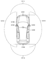
- FIG. 14 is a diagram illustrating an example of the installation position of the imaging unit 12031.
- imaging units 12101, 12102, 12103, 12104, and 12105 are provided as the imaging unit 12031.
- the imaging units 12101, 12102, 12103, 12104, and 12105 are provided, for example, on the front nose of the vehicle 12100, a side mirror, a rear bumper, a back door, an upper portion of a windshield of a vehicle interior, and the like.
- the imaging unit 12101 provided in the front nose and the imaging unit 12105 provided in the upper part of the windshield in the vehicle cabin mainly acquire an image in front of the vehicle 12100.
- the imaging units 12102 and 12103 included in the side mirror mainly acquire an image of the side of the vehicle 12100.
- the imaging unit 12104 provided in the rear bumper or the back door mainly acquires an image of the rear of the vehicle 12100.
- the imaging unit 12105 provided on the top of the windshield in the passenger compartment is mainly used to detect a leading vehicle or a pedestrian, an obstacle, a traffic light, a traffic sign, a lane, or the like.
- FIG. 14 shows an example of the imaging range of the imaging units 12101 to 12104.
- the imaging range 12111 indicates the imaging range of the imaging unit 12101 provided on the front nose
- the imaging ranges 12112 and 12113 indicate the imaging ranges of the imaging units 12102 and 12103 provided on the side mirrors
- the imaging range 12114 indicates The imaging range of the imaging part 12104 provided in the rear bumper or the back door is shown. For example, by overlaying the image data captured by the imaging units 12101 to 12104, a bird's eye view of the vehicle 12100 viewed from above can be obtained.
- At least one of the imaging units 12101 to 12104 may have a function of acquiring distance information.
- at least one of the imaging units 12101 to 12104 may be a stereo camera including a plurality of imaging devices, or an imaging device having pixels for phase difference detection.
- the microcomputer 12051 measures the distance to each three-dimensional object in the imaging ranges 12111 to 12114, and the temporal change of this distance (relative velocity with respect to the vehicle 12100). In particular, it is possible to extract a three-dimensional object traveling at a predetermined speed (for example, 0 km / h or more) in substantially the same direction as the vehicle 12100 as a leading vehicle, in particular by finding the it can. Further, the microcomputer 12051 can set an inter-vehicle distance to be secured in advance before the preceding vehicle, and can perform automatic brake control (including follow-up stop control), automatic acceleration control (including follow-up start control), and the like. As described above, it is possible to perform coordinated control for the purpose of automatic driving or the like that travels autonomously without depending on the driver's operation.
- automatic brake control including follow-up stop control
- automatic acceleration control including follow-up start control
- the microcomputer 12051 converts three-dimensional object data relating to three-dimensional objects into two-dimensional vehicles such as two-wheeled vehicles, ordinary vehicles, large vehicles, pedestrians, telephone poles, and other three-dimensional objects. It can be classified, extracted and used for automatic avoidance of obstacles. For example, the microcomputer 12051 identifies obstacles around the vehicle 12100 into obstacles visible to the driver of the vehicle 12100 and obstacles difficult to see.
- the microcomputer 12051 determines the collision risk indicating the degree of risk of collision with each obstacle, and when the collision risk is a setting value or more and there is a possibility of a collision, through the audio speaker 12061 or the display unit 12062 By outputting an alarm to the driver or performing forcible deceleration or avoidance steering via the drive system control unit 12010, driving support for collision avoidance can be performed.
- At least one of the imaging units 12101 to 12104 may be an infrared camera that detects infrared light.
- the microcomputer 12051 can recognize a pedestrian by determining whether a pedestrian is present in the images captured by the imaging units 12101 to 12104.
- pedestrian recognition is, for example, a procedure for extracting feature points in images captured by the imaging units 12101 to 12104 as an infrared camera, and pattern matching processing on a series of feature points indicating the outline of an object to determine whether it is a pedestrian or not
- the procedure is to determine
- the audio image output unit 12052 generates a square outline for highlighting the recognized pedestrian.
- the display unit 12062 is controlled so as to display a superimposed image. Further, the audio image output unit 12052 may control the display unit 12062 to display an icon or the like indicating a pedestrian at a desired position.
- the technology according to the present disclosure may be applied to the imaging unit 12031 among the configurations described above.
- the solid-state imaging device according to the present embodiment can be applied to the imaging unit 12031.
- the pixel array is A first pixel composed of a pair of sub-pixels arranged in the first direction under one microlens;
- a solid-state imaging device comprising at least one or more each.
- Each of the first pixel and the second pixel converts received light into an electric charge, and a photoelectric conversion unit provided for each of the pair of sub-pixels;
- An FD unit for storing charge output from each of the photoelectric conversion units, an amplification transistor whose on / off is controlled by the charge stored in the FD unit, a selection provided between the amplification transistor and the vertical signal line
- a signal processing circuit including a transistor and a reset transistor that resets the charge accumulated in the FD unit;
- the solid-state imaging device according to any one of (1) to (4), comprising: (6) The solid-state imaging device according to (5), wherein the FD unit is shared by each of the pair of sub-pixels constituting the first pixel and the second pixel.
- a solid-state imaging device having a pixel array in which a plurality of pixels each receiving light of a predetermined wavelength band is arranged,
- the pixel array is A first pixel composed of a pair of sub-pixels arranged in the first direction under one microlens;
- An electronic device including at least one or more of each.
- Pixel control transistor 50 Semiconductor substrate 100 First pixel 110, 120, 210, 220 Sub pixel 111, 121, 211, 221 Vertical type Gate electrode 140 240 Pixel wiring 150 250 Pixel transistor group 151 251 Amplification transistor 152 252 Selection transistor 153 Reset transistor 154 Dummy gate 200 Second pixel 500 Pixel array
Landscapes
- Engineering & Computer Science (AREA)
- Multimedia (AREA)
- Signal Processing (AREA)
- Physics & Mathematics (AREA)
- General Physics & Mathematics (AREA)
- Optics & Photonics (AREA)
- Solid State Image Pick-Up Elements (AREA)
- Focusing (AREA)
- Automatic Focus Adjustment (AREA)
- Transforming Light Signals Into Electric Signals (AREA)
Abstract
[Problème] Fournir un dispositif d'imagerie à semi-conducteur et un appareil électronique capables de réaliser une détection de mise au point et une génération d'image pour des sujets de diverses formes. À cet effet, l'invention concerne un dispositif d'imagerie à semi-conducteur qui comprend un réseau de pixels dans lequel une pluralité de pixels qui reçoivent chacun une lumière dans une bande de longueur d'onde prescrite sont agencés, le réseau de pixels comprenant au moins un de chaque pixel parmi : un premier pixel constitué par une paire de sous-pixels disposés côte à côte dans une première direction sous une microlentille ; et un second pixel constitué par une paire de sous-pixels disposés côte à côte dans une seconde direction orthogonale à la première direction sous une microlentille.
Priority Applications (1)
| Application Number | Priority Date | Filing Date | Title |
|---|---|---|---|
| US16/756,188 US11290665B2 (en) | 2017-10-24 | 2018-09-21 | Solid-state imaging device and electronic apparatus |
Applications Claiming Priority (2)
| Application Number | Priority Date | Filing Date | Title |
|---|---|---|---|
| JP2017-204912 | 2017-10-24 | ||
| JP2017204912A JP2019080141A (ja) | 2017-10-24 | 2017-10-24 | 固体撮像装置及び電子機器 |
Publications (1)
| Publication Number | Publication Date |
|---|---|
| WO2019082568A1 true WO2019082568A1 (fr) | 2019-05-02 |
Family
ID=66246442
Family Applications (1)
| Application Number | Title | Priority Date | Filing Date |
|---|---|---|---|
| PCT/JP2018/035176 Ceased WO2019082568A1 (fr) | 2017-10-24 | 2018-09-21 | Dispositif d'imagerie à semi-conducteur et appareil électronique |
Country Status (3)
| Country | Link |
|---|---|
| US (1) | US11290665B2 (fr) |
| JP (1) | JP2019080141A (fr) |
| WO (1) | WO2019082568A1 (fr) |
Cited By (2)
| Publication number | Priority date | Publication date | Assignee | Title |
|---|---|---|---|---|
| CN111586323A (zh) * | 2020-05-07 | 2020-08-25 | Oppo广东移动通信有限公司 | 图像传感器、控制方法、摄像头组件和移动终端 |
| JP2023088223A (ja) * | 2021-12-14 | 2023-06-26 | キヤノン株式会社 | 撮像装置およびその制御方法 |
Families Citing this family (1)
| Publication number | Priority date | Publication date | Assignee | Title |
|---|---|---|---|---|
| WO2021102832A1 (fr) * | 2019-11-28 | 2021-06-03 | Oppo广东移动通信有限公司 | Capteur d'image, procédé de commande, ensemble caméra et terminal mobile |
Citations (3)
| Publication number | Priority date | Publication date | Assignee | Title |
|---|---|---|---|---|
| JP2014072541A (ja) * | 2012-09-27 | 2014-04-21 | Nikon Corp | 撮像素子および撮像装置 |
| WO2016111175A1 (fr) * | 2015-01-07 | 2016-07-14 | ソニー株式会社 | Dispositif de traitement d'images, procédé de traitement d'images, et programme |
| WO2017130723A1 (fr) * | 2016-01-27 | 2017-08-03 | ソニー株式会社 | Élément de capture d'image à semiconducteur et dispositif électronique |
Family Cites Families (7)
| Publication number | Priority date | Publication date | Assignee | Title |
|---|---|---|---|---|
| JP5040960B2 (ja) * | 2009-06-04 | 2012-10-03 | 株式会社ニコン | 電子カメラ |
| JP5967950B2 (ja) * | 2011-04-20 | 2016-08-10 | キヤノン株式会社 | 撮像素子及び撮像装置 |
| JP5743837B2 (ja) * | 2011-10-07 | 2015-07-01 | キヤノン株式会社 | 光電変換装置、撮像装置および撮像システム |
| JP2013157883A (ja) * | 2012-01-31 | 2013-08-15 | Sony Corp | 固体撮像素子およびカメラシステム |
| JP6355362B2 (ja) | 2014-02-28 | 2018-07-11 | キヤノン株式会社 | 光電変換装置および撮像システム |
| CN208093559U (zh) * | 2015-09-17 | 2018-11-13 | 半导体元件工业有限责任公司 | 图像像素 |
| US10033949B2 (en) * | 2016-06-16 | 2018-07-24 | Semiconductor Components Industries, Llc | Imaging systems with high dynamic range and phase detection pixels |
-
2017
- 2017-10-24 JP JP2017204912A patent/JP2019080141A/ja active Pending
-
2018
- 2018-09-21 WO PCT/JP2018/035176 patent/WO2019082568A1/fr not_active Ceased
- 2018-09-21 US US16/756,188 patent/US11290665B2/en active Active
Patent Citations (3)
| Publication number | Priority date | Publication date | Assignee | Title |
|---|---|---|---|---|
| JP2014072541A (ja) * | 2012-09-27 | 2014-04-21 | Nikon Corp | 撮像素子および撮像装置 |
| WO2016111175A1 (fr) * | 2015-01-07 | 2016-07-14 | ソニー株式会社 | Dispositif de traitement d'images, procédé de traitement d'images, et programme |
| WO2017130723A1 (fr) * | 2016-01-27 | 2017-08-03 | ソニー株式会社 | Élément de capture d'image à semiconducteur et dispositif électronique |
Cited By (3)
| Publication number | Priority date | Publication date | Assignee | Title |
|---|---|---|---|---|
| CN111586323A (zh) * | 2020-05-07 | 2020-08-25 | Oppo广东移动通信有限公司 | 图像传感器、控制方法、摄像头组件和移动终端 |
| JP2023088223A (ja) * | 2021-12-14 | 2023-06-26 | キヤノン株式会社 | 撮像装置およびその制御方法 |
| JP7837711B2 (ja) | 2021-12-14 | 2026-03-31 | キヤノン株式会社 | 撮像装置およびその制御方法 |
Also Published As
| Publication number | Publication date |
|---|---|
| JP2019080141A (ja) | 2019-05-23 |
| US11290665B2 (en) | 2022-03-29 |
| US20210195124A1 (en) | 2021-06-24 |
Similar Documents
| Publication | Publication Date | Title |
|---|---|---|
| US20240258356A1 (en) | Imaging device and electronic apparatus | |
| US12191326B2 (en) | Solid-state imaging device | |
| JP7270616B2 (ja) | 固体撮像素子および固体撮像装置 | |
| JP7615246B2 (ja) | 撮像装置および電子機器 | |
| US12002825B2 (en) | Solid-state imaging device and electronic apparatus with improved sensitivity | |
| US12464838B2 (en) | Solid-state imaging device and electronic apparatus | |
| US11756971B2 (en) | Solid-state imaging element and imaging apparatus | |
| JP2023100745A (ja) | 固体撮像素子および撮像装置 | |
| US12557415B2 (en) | Imaging element and imaging device | |
| US20240395838A1 (en) | Imaging device | |
| US20260075974A1 (en) | Imaging device | |
| TW202040807A (zh) | 攝像裝置及攝像系統 | |
| US20240038807A1 (en) | Solid-state imaging device | |
| US11290665B2 (en) | Solid-state imaging device and electronic apparatus | |
| WO2022259855A1 (fr) | Dispositif à semi-conducteur, son procédé de fabrication et appareil électronique | |
| WO2019239754A1 (fr) | Élément d'imagerie à semi-conducteur, procédé de fabrication d'élément d'imagerie à semi-conducteur et dispositif électronique | |
| CN112771672A (zh) | 固态摄像元件、固态摄像装置和电子设备 | |
| EP4694177A1 (fr) | Dispositif de détection de lumière et appareil électronique | |
| US20260090117A1 (en) | Imaging device and electronic apparatus | |
| WO2019239767A1 (fr) | Dispositif de capture d'image | |
| WO2024057805A1 (fr) | Élément d'imagerie et dispositif électronique | |
| WO2025169695A1 (fr) | Dispositif de détection de lumière et appareil électronique | |
| WO2023058352A1 (fr) | Dispositif d'imagerie à semi-conducteurs |
Legal Events
| Date | Code | Title | Description |
|---|---|---|---|
| 121 | Ep: the epo has been informed by wipo that ep was designated in this application |
Ref document number: 18870498 Country of ref document: EP Kind code of ref document: A1 |
|
| NENP | Non-entry into the national phase |
Ref country code: DE |
|
| 122 | Ep: pct application non-entry in european phase |
Ref document number: 18870498 Country of ref document: EP Kind code of ref document: A1 |