WO2019082806A1 - Élément à ondes acoustiques - Google Patents
Élément à ondes acoustiquesInfo
- Publication number
- WO2019082806A1 WO2019082806A1 PCT/JP2018/038985 JP2018038985W WO2019082806A1 WO 2019082806 A1 WO2019082806 A1 WO 2019082806A1 JP 2018038985 W JP2018038985 W JP 2018038985W WO 2019082806 A1 WO2019082806 A1 WO 2019082806A1
- Authority
- WO
- WIPO (PCT)
- Prior art keywords
- substrate
- thickness
- piezoelectric layer
- elastic wave
- electrode
- Prior art date
- Legal status (The legal status is an assumption and is not a legal conclusion. Google has not performed a legal analysis and makes no representation as to the accuracy of the status listed.)
- Ceased
Links
Images






Classifications
-
- H—ELECTRICITY
- H03—ELECTRONIC CIRCUITRY
- H03H—IMPEDANCE NETWORKS, e.g. RESONANT CIRCUITS; RESONATORS
- H03H9/00—Networks comprising electromechanical or electro-acoustic elements; Electromechanical resonators
- H03H9/02—Details
- H03H9/125—Driving means, e.g. electrodes, coils
- H03H9/145—Driving means, e.g. electrodes, coils for networks using surface acoustic waves
-
- H—ELECTRICITY
- H03—ELECTRONIC CIRCUITRY
- H03H—IMPEDANCE NETWORKS, e.g. RESONANT CIRCUITS; RESONATORS
- H03H9/00—Networks comprising electromechanical or electro-acoustic elements; Electromechanical resonators
- H03H9/25—Constructional features of resonators using surface acoustic waves
Definitions
- the present invention relates to an elastic wave device.
- WO 2012/073871 proposes an elastic wave device including a support layer provided with a recess, a piezoelectric thin film disposed so as to extend onto the recess, and an IDT electrode formed on the piezoelectric thin film. ing.
- the elastic wave device of the present disclosure comprises an IDT electrode, a piezoelectric layer, and a substrate.
- the IDT electrode includes a plurality of electrode fingers.
- the piezoelectric layer is made of lithium tantalate single crystal having a thickness of less than 0.5 ⁇ , where ⁇ is a wavelength defined by twice the repetition interval of the plurality of electrode fingers, and the IDT electrode is located on the top surface.
- the substrate has a first surface which has a shear wave velocity V (m / s) of 5800 m / s or more and is bonded to the lower surface of the piezoelectric layer.
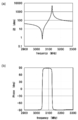
- FIGS. 3A and 3B are diagrams showing frequency characteristics of the acoustic wave device according to the present disclosure, respectively.
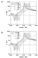
- FIGS. 4 (a) and 4 (b) are diagrams showing the frequency characteristics of the elastic wave element when the Euler angle of the piezoelectric layer is changed.
- FIGS. 5 (a) and 5 (b) are diagrams showing frequency characteristics of the acoustic wave device according to the reference example.
- FIGS. 6 (a) and 6 (b) are diagrams showing frequency characteristics of the acoustic wave device according to the reference example.
- FIGS. 8 (a) and 8 (b) are diagrams showing frequency characteristics of the acoustic wave device, respectively.
- 9 (a) and 9 (b) are diagrams showing frequency characteristics of the acoustic wave device.
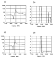
- FIGS. 11 (a) to 11 (d) are diagrams showing the frequency characteristics of the modification of the acoustic wave device shown in FIG. 1, respectively.
- FIGS. 17 (a) to 7 (c) are exploded top views showing each configuration of a modification of the acoustic wave device shown in FIG. It is a diagram which shows the relationship between the thickness of a piezoelectric layer, and a resonant frequency. It is a diagram which shows the relationship between the thickness of a piezoelectric layer, and a resonant frequency. It is a diagram which shows the relationship between the thickness of a piezoelectric layer, and a resonant frequency.
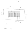
- the elastic wave device 1 (SAW device 1) according to the present embodiment includes a support substrate 10, a substrate 20, a piezoelectric layer 30, and an IDT electrode 4 as shown in FIG.
- the support substrate 10, the substrate 20, and the piezoelectric layer 30 are stacked in this order.
- the supporting substrate 10 supports the substrate 20 and the piezoelectric layer 30 located on the upper side, and the material is not limited as long as the strength is provided.
- a ceramic substrate, an organic substrate, a dielectric substrate such as quartz crystal or sapphire, a piezoelectric substrate, a semiconductor substrate, etc. can be exemplified, and it may be a substrate made of the same material system as the piezoelectric layer 30 described later. In this example, a single crystal silicon substrate is used.
- the thermal expansion coefficient is smaller than the material of the piezoelectric layer 30 described later. Therefore, when a temperature change occurs, a thermal stress is generated in the piezoelectric layer 30. At this time, the temperature dependency and the stress dependency of the elastic constant cancel each other, and the temperature change of the electrical characteristics of the SAW element 1 is reduced (temperature Special compensation).
- the thickness of the support substrate 10 is not particularly limited, but may be, for example, about 100 ⁇ m to 250 ⁇ m. The thickness decreases in the order of the support substrate 10, the substrate 20, the piezoelectric layer 30, and the IDT electrode 4 described later.
- the substrate 20 includes a first surface 20A and a second surface 20B opposite to the first surface 20A. Then, the second surface 20B is bonded to the upper surface of the support substrate 10, and the first surface 20A is bonded to the lower surface of the piezoelectric layer 30. In this example, the first surface 20A and the piezoelectric layer 30, and the second surface 20B and the support substrate 10 are directly bonded together, but the present invention is not limited to this. In particular, when the substrate 20 has a thickness equal to or greater than the wavelength ⁇ defined by twice the repetition interval Pt1 of the electrode finger 41 of the IDT electrode 4 described later, a bonding layer or the like is formed between the substrate 20 and the support substrate 10. It may be joined via
- the substrate 20 is made of a material having a shear wave velocity of 5800 m / s or more.
- a material having a shear wave velocity of 5800 m / s or more aluminum nitride (AlN), titanium nitride (TiN), silicon nitride (Si 3 N 4 ), silicon carbide (SiC), sapphire, alumina, boron nitride (BN), diamond, diamond like carbon ( DLC) etc. can be illustrated.
- the thickness of the substrate 20 is, for example, 0.8 ⁇ or more. More preferably, it is 1 ⁇ or more. Although the upper limit of the thickness of the substrate 20 is not particularly limited, in the case of forming the substrate 20 by a thin film process or the like, it may be 10 ⁇ or less in consideration of film forming property and the like.
- the piezoelectric layer 30 is located on the first surface 20 ⁇ / b> A of the substrate 20. In other words, the substrate 20 and the piezoelectric layer 30 are bonded directly or indirectly.
- the piezoelectric layer 30 is made of lithium tantalate single crystal (LiTaO 3 : sometimes abbreviated as LT below) having a thickness of less than 0.35 ⁇ .
- the Euler angles ( ⁇ , ⁇ , ⁇ ) are (90 ° ⁇ 0.5 °, 90 ° ⁇ 1 °, 20 ° to 50 °).
- the IDT electrode 4 is located on the top surface of the piezoelectric layer 30.
- the IDT electrode excites a surface acoustic wave, and as shown in FIG. 2, for example, constitutes a resonator composed of a pair of comb-like electrodes 40A and 40B.
- the comb-like electrode includes a plurality of electrode fingers 41.
- the electrode finger 41A connected to one potential and the electrode finger 41B connected to the other potential are alternately arranged so as to cross each other, and the SAW propagates along the arrangement direction of the electrode finger 41. .
- An interval between centers of widths of the electrode fingers 41A and 41B is referred to as a pitch Pt1.
- the width of the electrode finger 41 is w1 and the thickness thereof is s.
- an Al—Cu alloy As a material constituting such an IDT electrode 4, an Al—Cu alloy can be exemplified. The thickness is determined in consideration of the excitation efficiency of the SAW, the electromechanical coupling coefficient with the LT substrate, and the like. Further, the IDT electrode 4 may be a laminate of a plurality of electrode layers.
- the protective layer 6 is located on the top surface of the IDT electrode 4 in order to reduce its oxidation.
- Examples of the material of the protective layer 6 include inorganic insulating materials such as silicon oxide and silicon nitride.
- FIG. 3 (a) shows impedance characteristics with respect to frequency
- FIG. 3 (b) shows phase characteristics
- the horizontal axis represents frequency (unit: MHz)
- the vertical axis represents impedance (unit: ⁇ )
- the horizontal axis represents frequency (unit: MHz)
- the vertical axis represents impedance phase (unit: °).
- the basic configuration of the simulation model 1 is as follows.
- the most common SAW element in the prior art uses a 42 ° rotated YX propagation LT substrate having a thickness of 1 ⁇ or more as the piezoelectric layer 30 with an Euler angle of (0, -48, 0) There is.
- the pitch of the electrode fingers 41 is 1 ⁇ m
- the resonance frequency is about 2 GHz.
- the pitch of the electrode fingers 41 is 1 ⁇ m in the model 1 as shown in FIG. 3 by changing the thickness of the conventional SAW element and the piezoelectric layer 30 and the Euler angle. It was also confirmed that the resonance frequency could be 3.05 GHz.
- the value (sound velocity) obtained by multiplying the resonant frequency by ⁇ is 6000 m / s. From this, it can be confirmed that the resonator functions as a resonator using an elastic wave of a mode faster than the elastic wave of the mode used in the conventional SAW element.
- ⁇ f is as large as or larger than that of the conventional SAW element, and there is no bulk wave spurious between the resonant frequency and the antiresonant frequency. It was confirmed that a SAW device 1 with low loss and excellent in characteristics could be provided.
- the model 1 can provide the SAW element 1 with high frequency and less loss compared to the conventional SAW element even if the above-mentioned Euler angles are changed in the angle range of ⁇ 1 ° and ⁇ of ⁇ 2 °. It was confirmed.
- FIG. 4 shows changes in the impedance waveform of the resonator when the Euler angles ⁇ and ⁇ of the piezoelectric body are changed in the model 1.
- the horizontal axis is frequency (unit: MHz), and the vertical axis is impedance (unit: ⁇ ).
- the horizontal axis frequency of each impedance waveform is appropriately shifted (in fact, all the resonance frequencies are almost the same) for easy viewing.
- spurious noise occurs in the vicinity of resonance and antiresonance.
- occurrence of a small spurious is confirmed in the vicinity of the antiresonance frequency when ⁇ is ⁇ 1 ° and ⁇ is ⁇ 2 °.
- the influence of the spurious increases.
- generation of spurious was not confirmed when the range of ⁇ was ⁇ 0.5 ° and ⁇ was ⁇ 1 ° from the above Euler angle. From the above, high frequency characteristics can be provided by setting the range of ⁇ 0.5 ° and ⁇ to ⁇ 1 ° from the above-mentioned Euler angles.
- the SAW element 1 having a high frequency and less loss in the range of 20 ° to 50 ° compared to the conventional SAW element, but more specifically, the thickness of the electrode There is an appropriate range in relation to the thickness of the and the piezoelectric layer. This range will be described later.
- the substrate 20 is located on the entire lower surface of the piezoelectric layer 30, the handling is easy and the reliability can be high.
- the substrate 20 By making the substrate 20 a material having a cutoff frequency higher than the resonance frequency band of the resonator realized by the SAW element 1, leakage to the substrate 20 side is reduced, and the SAW element 1 with less loss is provided. can do.
- the cutoff frequency of AlN used as the substrate 20 in this example is 3.3 GHz.
- the thickness of AlN is reduced, part of the acoustic wave reaches the support substrate 10 and leaks. Therefore, the thickness of the substrate 20 needs to be at least 0.8 ⁇ or more, preferably 1 ⁇ or more.
- an adhesion layer or an adjustment layer for adjusting the characteristics may be inserted between the substrate 20 and the piezoelectric layer 30.
- the substrate 20 is 1 ⁇ , and the supporting substrate 10 made of Si is provided on the lower surface thereof.
- the thermal stress due to Si having a small thermal expansion coefficient is applied to the piezoelectric layer 30, so that it is possible to obtain the SAW element 1 in which the characteristic change due to the temperature change is reduced.
- FIG. 5A is a graph showing impedance characteristics with respect to frequency.
- the vertical axis represents impedance (unit: ⁇ ), and the horizontal axis represents frequency (unit: MHz).
- 5B is a diagram showing phase characteristics with respect to frequency, in which the vertical axis is phase (unit: °) and the horizontal axis is frequency (unit: MHz).
- the impedance phase characteristic in the vicinity of the antiresonance rises more than -90 °. This indicates that a large loss occurs in this frequency range.
- FIG. 6 (a) and 6 (b) correspond to FIGS. 5 (a) and 5 (b). In this case, a large spurious vibration is generated on the high frequency side than the antiresonance.
- the thickness of the piezoelectric layer 30 has an appropriate range, and the range is related to the Euler angle of the piezoelectric layer 30 and the thickness of the electrode 4.
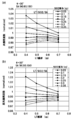
- FIG. 7 is a result of simulating a change in impedance characteristics with respect to the thickness of the piezoelectric layer 30 and the thickness of the electrode 4 when the Euler angle of the piezoelectric layer 30 is changed.
- the horizontal axis represents the thickness of the electrode 4 and the vertical axis represents the thickness of the piezoelectric layer 30, and the region (R1) with a good parameter of the impedance waveform is filled for each ridge.
- a region indicated as SP in FIG. 7 is a region where a large spurious vibration occurs as shown in FIG.
- a region indicated by LS is a region where a large loss occurs in the impedance characteristic as shown in FIG.
- the filled area R1 excluding this area is a range in which good impedance characteristics are obtained.
- a dark color portion and a light color portion exist in the region R1.
- the thickness of the electrode 4, the thickness of the electrode 4 and the thickness of the piezoelectric layer 30 are adjusted so as to be the area of the dark color part of the area R1 in consideration of the manufacturing variation and the like. It is also good.
- FIG. 7 will be described in detail.
- the combination of the electrode thickness and the thickness of the piezoelectric layer 30 which is in the region R1 but outside the range of the region R1 in the case of the next level angle is adjacent It is assumed that it is outside the region R1 between the angles of the eyebrows.
- the combination of the electrode thickness of model 1: 0.07 ⁇ and the thickness of piezoelectric layer 30: 0.25 ⁇ it is located within the R1 region regardless of whether ⁇ is -10 ° to 60 °. .
- the impedance characteristics of the SAW element 1 appear spurious with a slight change with respect to the Euler angles ⁇ and ⁇ , but as can be seen from FIG. does not change. However, when ⁇ changes significantly, the resonance frequency fr and the frequency difference df (anti-resonance frequency fa ⁇ resonance frequency fr) change.
- the thickness of the piezoelectric layer 30 is fixed at 0.25 ⁇ with the parameters of the model 1, and the changes in fr and df when the thickness of the electrode 4 is changed are shown for each ridge. It shows what was plotted.
- the horizontal axis is frequency (unit: MHz), and the vertical axis is impedance (unit: ⁇ ).
- FIG. 9 (a) and 9 (b) when the thickness of the electrode 4 is fixed to 0.07 ⁇ by the parameter of the model 1 and the thickness of the piezoelectric layer 30 is changed, the changes between fr and df are shown in FIG. It shows what was plotted about.
- the horizontal axis is frequency (unit: MHz), and the vertical axis is impedance (unit: ⁇ ).
- fr increases while df decreases slightly.
- the thickness of the piezoelectric layer 30 is 0.225 ⁇ . It is desirable that ⁇ 0.3 ⁇ .
- the SAW element 1 having the support substrate 10 has been described.
- the substrate 20 since the thickness of the substrate 20 has no upper limit in electrical characteristics, the substrate 20 can be thickened to have the function as the support substrate 10
- the support substrate 10 may be omitted.
- an AlN substrate, a sapphire substrate or the like in which the substrate 20 has a thickness of about 50 ⁇ m to 250 ⁇ m may be used.
- an adhesion layer or an adjustment layer for adjusting the characteristics may be inserted between the substrate 20 and the piezoelectric layer 30.
- the support substrate 10 may be made of sapphire single crystal and the substrate 20 may be made of AlN.
- both the support substrate 10 and the substrate 2 become an Al-based material. Therefore, when the support substrate 10 and the substrate 20 are bonded and bonded, the mismatch of the bonding interface can be reduced, so the loss of elastic waves can be reduced. Further, since strong bonding can be realized, reliability can be improved.
- the interface mismatch can be reduced, and the quality of the film to be formed can be enhanced, and the loss of elastic waves It can be reduced.
- the piezoelectric layer 30 has two thicknesses of 0.3 ⁇ and 0.5 ⁇ , and an Euler angle of (86 ° to 94 °, 86 ° to 94 °, ⁇ 10 ° to 70 °).
- the frequency characteristics were simulated by setting the thickness of V to 0.04 ⁇ to 0.08 ⁇ .
- the thickness of the electrode 4 was changed to check the position and the magnitude of fr and spurious. As a result, the influence of the thickness of the electrode 4 was not confirmed for the magnitude of fr and spurious. However, it was confirmed that the position of the spurious shifts to the higher frequency side as the thickness of the electrode 4 is thinner. From the result, the thickness of the electrode 4 may be 0.04 ⁇ to 0.08 ⁇ . When it is 0.04 ⁇ or more, resonance characteristics can be obtained without deterioration of the resistance as an electrode. When the wavelength is 0.08 ⁇ or less, the position of the spurious is about 3500 MHz, and the resonance characteristics can be obtained without deterioration of the loss on the side higher than the antiresonance frequency.
- the positions of fr, df and spurious are also used when using a ceramic SiC substrate And there was no difference in strength, loss, etc. Further, in both of the single crystal SiC substrate and the ceramic SiC substrate, no change in the characteristics was observed even when rotated in the plane direction with respect to the propagation direction of the SAW (when the crucible of the SiC substrate was rotated). . That is, in the case where SiC is used as the substrate 20 in the SAW element 1, it is possible to provide the SAW element 1 having stable characteristics without being strongly affected by various parameters including the crystallinity of the substrate.
- SiC is a semiconductor and generally has conductivity. As the conductivity increases, the SAW characteristics are affected, so the conductivity of the SiC substrate should be high. Specifically, the conductivity of the SiC substrate may be 1 k ⁇ cm or more.
- the piezoelectric layer 30 has two thicknesses of 0.3 ⁇ and 0.5 ⁇ , and an Euler angle of (86 ° to 94 °, 86 ° to 94 °, ⁇ 10 ° to 70 °).
- the thickness of each was 0.04 ⁇ to 0.08 ⁇ , and the frequency characteristics were simulated by combining the respective conditions.
- FIGS. 11A and 11B show frequency characteristics when the substrate 20 is made of sapphire. Further, as reference examples, frequency characteristics when the substrate 20 is made of alumina are shown in FIGS. 11 (c) and 11 (d).
- the horizontal axis represents frequency
- the vertical axis represents impedance.
- the horizontal axis indicates the frequency
- the vertical axis indicates the phase.
- the thickness of the piezoelectric layer 30 is 0.3 ⁇ , the Euler angles (90 °, 90 °, 30 °), and the Euler angles of the substrate 20 are changed to (90 °, 90 °, 120 ° to 170 °). It shows the frequency characteristics in the case of The upper stage shows impedance characteristics, and the lower stage shows phase characteristics.
- middle layer 50 may be made to intervene.
- the intermediate layer 50 is made of a material in which the acoustic velocity of the elastic wave propagating through the piezoelectric layer 30 is smaller than that of the piezoelectric layer 30 and the substrate 20.
- a material is, for example, SiO 2 .
- the thickness thereof is thinner than that of the piezoelectric layer 30, and may be, for example, 0.08 ⁇ to 0.1 ⁇ .
- the intermediate layer 50 having a low sound velocity
- the vibration of the elastic wave propagating in the piezoelectric layer 30 is moved to the intermediate layer 50 in a large amount.
- the acoustic velocity of the elastic wave is reduced.
- the resonance frequency shifts to the high frequency side.
- the elastic wave moves to the intermediate layer 50 as the thickness of the piezoelectric layer 30 becomes thinner, and as a result, the speed of sound becomes slower and the resonance frequency becomes lower.
- the effect of increasing the resonant frequency by thinning the piezoelectric layer 30 and the effect of decreasing the resonant frequency by thinning the piezoelectric layer 30 cancel each other.
- the elastic wave element 1 with high robustness can be provided in which the resonance frequency does not change.
- FIG. 18 shows the same result when the substrate 20 is SiC when the substrate 20 is sapphire single crystal, but the result is almost similar to the case of AlN shown in FIG.
- the SAW element 1 may include a capacitance unit 60 connected in parallel to the IDT electrode 4. Since the capacitance portion 60 can reduce df, it can be adjusted to have a desired df.
- a capacitive portion 60 is formed of an interdigital electrode similar to the IDT electrode 4, the repetitive arrangement direction D1 of the electrode fingers 43 (capacitive portion electrode fingers 43) of the capacitive portion functions as a resonator.
- the arrangement direction D 2 of the electrode fingers 41 of the IDT electrode 4 may be different. With such a configuration, the influence of the resonance by the capacitive section 60 can be reduced.
- the arrangement direction D1 is -60 ° ⁇ 5 °, 60 ° ⁇ 5 °, the frequency is higher than fr. The maximum intensity of the located spurs can be lowered.
- the (111) plane of Si is (-45 °, -54.7 °, ⁇ ) in Euler angles.
- the maximum intensity of the spurious was simulated when ⁇ was changed. The results are shown in FIG. In FIG. 16, the horizontal axis is the arrangement direction D 1 and the vertical axis is ⁇ , and the maximum intensity of the spurious is indicated by contour lines. As apparent from FIG. 16, the spurious intensity can be reduced when the wedge of the support substrate 10 is set to 0 ° to 20 °, 40 ° to 140 °, and 160 ° to 180 °.
- FIG. 17A is a view of the piezoelectric layer 30 from the top
- FIG. 17B is a view of the substrate 20 from the top
- FIG. 17C is a view of the support substrate 10 from the top.
- FIG. 17A also shows a schematic view showing the arrangement relationship between the IDT electrode 4 and the capacitor portion 60 disposed on the piezoelectric layer 30. As shown in FIG.
- the cutoff frequency of the substrate 20 is increased to reduce the loss on the high frequency side relative to the antiresonance frequency, and the intensity of the spurious generated on the high frequency side relative to the antiresonance frequency is also obtained. It can be reduced.
- Elastic wave element 20 Substrate 30: Piezoelectric layer 4: IDT electrode 41: Electrode finger
Landscapes
- Physics & Mathematics (AREA)
- Acoustics & Sound (AREA)
- Surface Acoustic Wave Elements And Circuit Networks Thereof (AREA)
Abstract
L'invention concerne un élément à ondes acoustiques 1 pourvu : d'une électrode IDT 4 comprenant une pluralité de doigts d'électrode 41 ; d'une couche piézoélectrique 30 comportant l'électrode IDT 4 positionnée sur sa surface supérieure, ayant une épaisseur inférieure à 0,35 λ, λ représentant une longueur d'onde définie par deux fois l'intervalle de répétition des doigts d'électrode 41, qui est constituée d'un monocristal de tantalite de lithium, et qui a des angles d'Euler de 90 ±1, de 90 ±2, de 20 à 50 ; et d'un substrat 20 dans lequel une vitesse acoustique d'onde transversale V (m/s) est supérieure ou égale à 5800 m/s et comportant une première surface jointe à la surface inférieure de la couche piézoélectrique 30.
Priority Applications (1)
| Application Number | Priority Date | Filing Date | Title |
|---|---|---|---|
| JP2019551094A JP7073392B2 (ja) | 2017-10-23 | 2018-10-19 | 弾性波素子 |
Applications Claiming Priority (2)
| Application Number | Priority Date | Filing Date | Title |
|---|---|---|---|
| JP2017204478 | 2017-10-23 | ||
| JP2017-204478 | 2017-10-23 |
Publications (1)
| Publication Number | Publication Date |
|---|---|
| WO2019082806A1 true WO2019082806A1 (fr) | 2019-05-02 |
Family
ID=66246485
Family Applications (1)
| Application Number | Title | Priority Date | Filing Date |
|---|---|---|---|
| PCT/JP2018/038985 Ceased WO2019082806A1 (fr) | 2017-10-23 | 2018-10-19 | Élément à ondes acoustiques |
Country Status (2)
| Country | Link |
|---|---|
| JP (1) | JP7073392B2 (fr) |
| WO (1) | WO2019082806A1 (fr) |
Cited By (4)
| Publication number | Priority date | Publication date | Assignee | Title |
|---|---|---|---|---|
| WO2020050401A1 (fr) * | 2018-09-07 | 2020-03-12 | 株式会社村田製作所 | Dispositif à onde élastique, circuit frontal haute fréquence et dispositif de communication |
| JP2021044738A (ja) * | 2019-09-12 | 2021-03-18 | 京セラ株式会社 | 弾性波素子 |
| WO2021090775A1 (fr) * | 2019-11-06 | 2021-05-14 | 株式会社村田製作所 | Dispositif à ondes élastiques |
| CN119010830A (zh) * | 2024-10-22 | 2024-11-22 | 泉州市三安集成电路有限公司 | 弹性波器件及模组 |
Citations (9)
| Publication number | Priority date | Publication date | Assignee | Title |
|---|---|---|---|---|
| JPH08316781A (ja) * | 1995-05-17 | 1996-11-29 | Yasutaka Shimizu | 弾性表面波素子 |
| JPH10178331A (ja) * | 1996-12-19 | 1998-06-30 | Matsushita Electric Ind Co Ltd | 弾性表面波素子 |
| JP2006025396A (ja) * | 2004-06-09 | 2006-01-26 | Seiko Epson Corp | 弾性表面波装置、その製造方法、および電子機器 |
| JP2006524016A (ja) * | 2003-03-03 | 2006-10-19 | クリー インコーポレイテッド | 窒化物ベースの集積音波デバイスおよび窒化物ベースの集積音波デバイスを製造する方法 |
| WO2011037145A1 (fr) * | 2009-09-25 | 2011-03-31 | 株式会社村田製作所 | Dispositif a ondes acoustiques de surface |
| WO2012086441A1 (fr) * | 2010-12-24 | 2012-06-28 | 株式会社村田製作所 | Dispositif à ondes élastiques et procédé de fabrication correspondant |
| JP3187231U (ja) * | 2013-09-05 | 2013-11-14 | 日本碍子株式会社 | 複合基板 |
| WO2016104598A1 (fr) * | 2014-12-26 | 2016-06-30 | 京セラ株式会社 | Dispositif à onde acoustique |
| WO2018097016A1 (fr) * | 2016-11-25 | 2018-05-31 | 国立大学法人東北大学 | Dispositif à ondes élastiques |
Family Cites Families (2)
| Publication number | Priority date | Publication date | Assignee | Title |
|---|---|---|---|---|
| KR100904368B1 (ko) * | 2005-10-19 | 2009-06-23 | 가부시키가이샤 무라타 세이사쿠쇼 | 램파 디바이스 |
| DE112015001242B4 (de) * | 2014-03-14 | 2024-07-25 | Murata Manufacturing Co., Ltd. | Vorrichtung für elastische Wellen |
-
2018
- 2018-10-19 JP JP2019551094A patent/JP7073392B2/ja active Active
- 2018-10-19 WO PCT/JP2018/038985 patent/WO2019082806A1/fr not_active Ceased
Patent Citations (9)
| Publication number | Priority date | Publication date | Assignee | Title |
|---|---|---|---|---|
| JPH08316781A (ja) * | 1995-05-17 | 1996-11-29 | Yasutaka Shimizu | 弾性表面波素子 |
| JPH10178331A (ja) * | 1996-12-19 | 1998-06-30 | Matsushita Electric Ind Co Ltd | 弾性表面波素子 |
| JP2006524016A (ja) * | 2003-03-03 | 2006-10-19 | クリー インコーポレイテッド | 窒化物ベースの集積音波デバイスおよび窒化物ベースの集積音波デバイスを製造する方法 |
| JP2006025396A (ja) * | 2004-06-09 | 2006-01-26 | Seiko Epson Corp | 弾性表面波装置、その製造方法、および電子機器 |
| WO2011037145A1 (fr) * | 2009-09-25 | 2011-03-31 | 株式会社村田製作所 | Dispositif a ondes acoustiques de surface |
| WO2012086441A1 (fr) * | 2010-12-24 | 2012-06-28 | 株式会社村田製作所 | Dispositif à ondes élastiques et procédé de fabrication correspondant |
| JP3187231U (ja) * | 2013-09-05 | 2013-11-14 | 日本碍子株式会社 | 複合基板 |
| WO2016104598A1 (fr) * | 2014-12-26 | 2016-06-30 | 京セラ株式会社 | Dispositif à onde acoustique |
| WO2018097016A1 (fr) * | 2016-11-25 | 2018-05-31 | 国立大学法人東北大学 | Dispositif à ondes élastiques |
Cited By (9)
| Publication number | Priority date | Publication date | Assignee | Title |
|---|---|---|---|---|
| WO2020050401A1 (fr) * | 2018-09-07 | 2020-03-12 | 株式会社村田製作所 | Dispositif à onde élastique, circuit frontal haute fréquence et dispositif de communication |
| US11855609B2 (en) | 2018-09-07 | 2023-12-26 | Murata Manufacturing Co., Ltd. | Acoustic wave device, radio-frequency front end circuit, and communication device |
| JP2021044738A (ja) * | 2019-09-12 | 2021-03-18 | 京セラ株式会社 | 弾性波素子 |
| JP7401999B2 (ja) | 2019-09-12 | 2023-12-20 | 京セラ株式会社 | 弾性波素子 |
| WO2021090775A1 (fr) * | 2019-11-06 | 2021-05-14 | 株式会社村田製作所 | Dispositif à ondes élastiques |
| JPWO2021090775A1 (fr) * | 2019-11-06 | 2021-05-14 | ||
| JP7392734B2 (ja) | 2019-11-06 | 2023-12-06 | 株式会社村田製作所 | 弾性波装置 |
| US12537508B2 (en) | 2019-11-06 | 2026-01-27 | Murata Manufacturing Co., Ltd. | Acoustic wave device |
| CN119010830A (zh) * | 2024-10-22 | 2024-11-22 | 泉州市三安集成电路有限公司 | 弹性波器件及模组 |
Also Published As
| Publication number | Publication date |
|---|---|
| JPWO2019082806A1 (ja) | 2020-10-22 |
| JP7073392B2 (ja) | 2022-05-23 |
Similar Documents
| Publication | Publication Date | Title |
|---|---|---|
| JP6856825B2 (ja) | 弾性波装置、分波器および通信装置 | |
| CN103891139B (zh) | 弹性表面波装置 | |
| JP5099151B2 (ja) | 弾性境界波装置の製造方法 | |
| CN109075770B (zh) | 复合基板以及使用其的弹性波元件 | |
| JP4337816B2 (ja) | 弾性境界波装置 | |
| JP7278305B2 (ja) | 弾性波装置、分波器および通信装置 | |
| JP6915076B2 (ja) | 複合基板、およびそれを用いた弾性波素子 | |
| JP7433873B2 (ja) | 弾性波共振器、フィルタ、及びマルチプレクサ | |
| JP6854891B2 (ja) | 弾性波装置、分波器および通信装置 | |
| US8476984B2 (en) | Vibration device, oscillator, and electronic apparatus | |
| JPWO2005086345A1 (ja) | 弾性境界波装置 | |
| JP7466562B2 (ja) | 弾性波装置 | |
| JP7624796B2 (ja) | ラダー型フィルタおよびマルチプレクサ | |
| JP7073392B2 (ja) | 弾性波素子 | |
| CN113454912B (zh) | 弹性波装置 | |
| WO2024043343A1 (fr) | Dispositif à ondes acoustiques | |
| JP7493306B2 (ja) | 弾性波装置 | |
| WO2022230723A1 (fr) | Dispositif à ondes élastiques | |
| US20240014793A1 (en) | Acoustic wave device and method for manufacturing acoustic wave device | |
| JP5039362B2 (ja) | 弾性波デバイス | |
| JP2023166577A (ja) | 弾性波素子 | |
| WO2025070641A1 (fr) | Dispositif de filtre | |
| WO2025100131A1 (fr) | Dispositif à ondes élastiques | |
| JP2026005000A (ja) | 弾性波装置 |
Legal Events
| Date | Code | Title | Description |
|---|---|---|---|
| 121 | Ep: the epo has been informed by wipo that ep was designated in this application |
Ref document number: 18871174 Country of ref document: EP Kind code of ref document: A1 |
|
| ENP | Entry into the national phase |
Ref document number: 2019551094 Country of ref document: JP Kind code of ref document: A |
|
| NENP | Non-entry into the national phase |
Ref country code: DE |
|
| 122 | Ep: pct application non-entry in european phase |
Ref document number: 18871174 Country of ref document: EP Kind code of ref document: A1 |