WO2019082932A1 - Procédé de fabrication de module de conversion thermoélectrique, module de conversion thermoélectrique, et liant pour module de conversion thermoélectrique - Google Patents
Procédé de fabrication de module de conversion thermoélectrique, module de conversion thermoélectrique, et liant pour module de conversion thermoélectriqueInfo
- Publication number
- WO2019082932A1 WO2019082932A1 PCT/JP2018/039507 JP2018039507W WO2019082932A1 WO 2019082932 A1 WO2019082932 A1 WO 2019082932A1 JP 2018039507 W JP2018039507 W JP 2018039507W WO 2019082932 A1 WO2019082932 A1 WO 2019082932A1
- Authority
- WO
- WIPO (PCT)
- Prior art keywords
- bonding
- thermoelectric conversion
- conversion module
- type semiconductor
- copper particles
- Prior art date
- Legal status (The legal status is an assumption and is not a legal conclusion. Google has not performed a legal analysis and makes no representation as to the accuracy of the status listed.)
- Ceased
Links
Images
Classifications
-
- H—ELECTRICITY
- H10—SEMICONDUCTOR DEVICES; ELECTRIC SOLID-STATE DEVICES NOT OTHERWISE PROVIDED FOR
- H10N—ELECTRIC SOLID-STATE DEVICES NOT OTHERWISE PROVIDED FOR
- H10N10/00—Thermoelectric devices comprising a junction of dissimilar materials, i.e. devices exhibiting Seebeck or Peltier effects
- H10N10/01—Manufacture or treatment
-
- B—PERFORMING OPERATIONS; TRANSPORTING
- B22—CASTING; POWDER METALLURGY
- B22F—WORKING METALLIC POWDER; MANUFACTURE OF ARTICLES FROM METALLIC POWDER; MAKING METALLIC POWDER; APPARATUS OR DEVICES SPECIALLY ADAPTED FOR METALLIC POWDER
- B22F7/00—Manufacture of composite layers, workpieces, or articles, comprising metallic powder, by sintering the powder, with or without compacting wherein at least one part is obtained by sintering or compression
- B22F7/06—Manufacture of composite layers, workpieces, or articles, comprising metallic powder, by sintering the powder, with or without compacting wherein at least one part is obtained by sintering or compression of composite workpieces or articles from parts, e.g. to form tipped tools
- B22F7/08—Manufacture of composite layers, workpieces, or articles, comprising metallic powder, by sintering the powder, with or without compacting wherein at least one part is obtained by sintering or compression of composite workpieces or articles from parts, e.g. to form tipped tools with one or more parts not made from powder
-
- C—CHEMISTRY; METALLURGY
- C22—METALLURGY; FERROUS OR NON-FERROUS ALLOYS; TREATMENT OF ALLOYS OR NON-FERROUS METALS
- C22C—ALLOYS
- C22C19/00—Alloys based on nickel or cobalt
- C22C19/03—Alloys based on nickel or cobalt based on nickel
-
- C—CHEMISTRY; METALLURGY
- C22—METALLURGY; FERROUS OR NON-FERROUS ALLOYS; TREATMENT OF ALLOYS OR NON-FERROUS METALS
- C22C—ALLOYS
- C22C5/00—Alloys based on noble metals
- C22C5/02—Alloys based on gold
-
- C—CHEMISTRY; METALLURGY
- C22—METALLURGY; FERROUS OR NON-FERROUS ALLOYS; TREATMENT OF ALLOYS OR NON-FERROUS METALS
- C22C—ALLOYS
- C22C5/00—Alloys based on noble metals
- C22C5/04—Alloys based on a platinum group metal
-
- C—CHEMISTRY; METALLURGY
- C22—METALLURGY; FERROUS OR NON-FERROUS ALLOYS; TREATMENT OF ALLOYS OR NON-FERROUS METALS
- C22C—ALLOYS
- C22C5/00—Alloys based on noble metals
- C22C5/06—Alloys based on silver
-
- C—CHEMISTRY; METALLURGY
- C22—METALLURGY; FERROUS OR NON-FERROUS ALLOYS; TREATMENT OF ALLOYS OR NON-FERROUS METALS
- C22C—ALLOYS
- C22C9/00—Alloys based on copper
-
- C—CHEMISTRY; METALLURGY
- C22—METALLURGY; FERROUS OR NON-FERROUS ALLOYS; TREATMENT OF ALLOYS OR NON-FERROUS METALS
- C22C—ALLOYS
- C22C9/00—Alloys based on copper
- C22C9/06—Alloys based on copper with nickel or cobalt as the next major constituent
-
- H—ELECTRICITY
- H10—SEMICONDUCTOR DEVICES; ELECTRIC SOLID-STATE DEVICES NOT OTHERWISE PROVIDED FOR
- H10N—ELECTRIC SOLID-STATE DEVICES NOT OTHERWISE PROVIDED FOR
- H10N10/00—Thermoelectric devices comprising a junction of dissimilar materials, i.e. devices exhibiting Seebeck or Peltier effects
- H10N10/80—Constructional details
- H10N10/81—Structural details of the junction
- H10N10/817—Structural details of the junction the junction being non-separable, e.g. being cemented, sintered or soldered
Definitions
- the present invention relates to a method of manufacturing a thermoelectric conversion module, a thermoelectric conversion module, and a bonding material for a thermoelectric conversion module.
- thermoelectric conversion module using a thermoelectric semiconductor of p-type semiconductor and n-type semiconductor as a thermoelectric conversion material is simple in structure and has no movable part, so it has high reliability and easy maintenance and inspection.
- a power generation system is a small-scale distributed power generation system using an exhaust heat source such as a waste incinerator or a cogeneration system, an on-vehicle power generation using the heat of exhaust gas from an automobile, etc.
- Application to a system is expected, and reduction of the unit price of power generation and improvement of the durability of the thermoelectric conversion system are desired.
- the thermoelectric conversion module has, for example, an electrode made of copper or the like joined to both sides of a thermoelectric semiconductor, an electric insulating layer made of mica or the like provided on the other surface of the electrode, and layers stacked on the respective electric insulating layers. It has a high temperature side heat source and a low temperature side heat source (for example, refer to the following patent documents 1).
- a temperature difference is provided at both ends of the thermoelectric conversion element by supplying a high temperature exhaust gas or the like to the low temperature side heat source while blowing air to the low temperature side heat source.
- a thermoelectromotive force can be generated inside the thermoelectric conversion element to extract a direct current from the electrode.
- thermoelectric conversion module having the above configuration, the thermoelectric semiconductor and the high temperature side electrode or the low temperature side electrode are generally joined by a bonding material such as a brazing material and a solder.
- the electromotive force of the thermoelectric conversion module is proportional to the temperature difference inside the thermoelectric semiconductor generated between the high temperature side electrode and the low temperature side electrode. Therefore, the heat conduction property of the bonding material also affects the temperature difference in the thermoelectric semiconductor, that is, the power generation performance.
- the thermal conductivity of a bonding material such as a brazing material or a solder may be lower than that of the electrode, which may lead to a decrease in power generation performance.
- thermoelectric semiconductor is a brittle material, if a large thermal expansion difference occurs between the electrode and the thermoelectric semiconductor during bonding or operation, destruction of the thermoelectric semiconductor may be caused to break the circuit. Since the brazing material and the solder have a low stress absorbing effect, it is difficult to suppress the above problems.
- thermoelectric semiconductor if variations occur in the position of the junction surface with the electrodes of the thermoelectric semiconductor or the distance between the electrodes due to the variation in the length of the thermoelectric semiconductor, the surface pressure distribution will occur when pressing the electrodes and the thermoelectric semiconductor at the time of joining. The adhesion is aggravated as it occurs. If the adhesion between the thermoelectric semiconductor and the electrode is poor, the contact thermal resistance increases and the electrical conductivity decreases, so the power generation performance decreases. Usually, in order to ensure sufficient adhesion between the thermoelectric semiconductor and the electrode, assembly is carried out using the thermoelectric semiconductor sorted so that the variation in length is about 10 ⁇ m or less, or an electrode with small deformation and small surface roughness. It will be. As described above, when there is a variation in the length of the thermoelectric semiconductor, additional processing such as processing for selecting work and, in some cases, processing for adjusting the position (height) of the joint surface occurs, which increases the manufacturing cost. It will be easier.
- the present invention has been made in view of the above circumstances, and can produce a thermoelectric conversion module excellent in power generation performance and thermal stress characteristics with high productivity even when the length of the thermoelectric semiconductor varies. It is an object of the present invention to provide a method of manufacturing a thermoelectric conversion module, a thermoelectric conversion module excellent in power generation performance and thermal stress characteristics, and a bonding material for a thermoelectric conversion module used for these.
- the present invention electrically connects in series a thermoelectric semiconductor portion in which a plurality of p-type semiconductors and n-type semiconductors are alternately arranged, an adjacent p-type semiconductor and an n-type semiconductor, p Of thermoelectric conversion module with high temperature side electrode joined to junction surface of high temperature heat source side of n-type semiconductor and n type semiconductor and low temperature side electrode joined to junction surface of low temperature heat source side of p type semiconductor and n type semiconductor A bonding layer including metal particles provided between at least one of the high-temperature side electrode and the low-temperature side electrode, the p-type semiconductor and the n-type semiconductor.
- the manufacturing method of the thermoelectric conversion module provided with the joining process of joining by the said, and the said joining layer is formed of the joining material which contains a copper particle as said metal particle is provided.
- the manufacturing method of the present invention by sintering the bonding layer containing copper particles, the thermal resistance can be reduced as compared with the brazing material, and a thermoelectric conversion module excellent in power generation performance can be obtained.
- the sintered bonding layer is a porous body, it is possible to reduce the stress caused by the thermal expansion difference between the thermoelectric semiconductor and the electrode during bonding or operation.
- the bonding layer has shape following property, even when there is variation in the length of the thermoelectric semiconductor, sufficient adhesion between the thermoelectric semiconductor and the electrode can be obtained. Thereby, the yield of the thermoelectric conversion module can be improved.
- thermoelectric conversion module obtained by the manufacturing method according to the present invention comprises a sintered body formed by sintering a bonding layer containing copper particles, whereby a temperature of ⁇ 50 ° C. to 1085 ° C., which is the melting point of copper. It can be used in the temperature range of According to the manufacturing method of the present invention, it is possible to manufacture a thermoelectric conversion module that can be used even in a high temperature environment of 300 ° C. or higher, which is difficult in solder bonding.
- the bonding layer can be sintered under a load of 0 to 100 MPa.
- the bonding layer is formed of a coating film of the bonding material with a thickness of 10 ⁇ m to 1000 ⁇ m from the viewpoint of stress relaxation effect, thermal variation of the length of the thermoelectric semiconductor or variation of distance between the electrodes, and printing accuracy. It may be one. It becomes easy to acquire a stress relaxation effect as the thickness of a coating film is 10 micrometers or more, and it becomes easy to secure printing accuracy as it is 1000 micrometers or less.
- the variation in length in the current direction of the p-type semiconductor and the n-type semiconductor before bonding may be 10 to 200 ⁇ m. Even when there is a variation in the length of such a thermoelectric semiconductor, the adhesion between the thermoelectric semiconductor and the electrode can be sufficiently obtained by the bonding layer having shape following property. Moreover, it becomes easy to adjust the height of the thermoelectric conversion module after joining in a predetermined range. As a result, the yield of the thermoelectric conversion module can be improved, and the cost of the thermoelectric conversion module can be reduced.
- bonding surfaces of the p-type semiconductor and the n-type semiconductor to the high temperature side electrode and the low temperature side electrode, and bonding surfaces of the high temperature side electrode and the low temperature side electrode to the p type semiconductor and the n type semiconductor, A part or all of at least one surface of the metal may have a metal diffusion prevention layer.
- thermoelectric semiconductor By providing the metal diffusion prevention layer, it is possible to prevent the deterioration of the power generation performance due to the diffusion of the metal component contained in the thermoelectric semiconductor.
- the bonding material may further include a dispersion medium.
- the bonding material may include a solvent having a boiling point of 300 ° C. or more as a dispersion medium, 2% by mass or more based on the total mass of the bonding material, or 15% by volume or more based on the total volume of the bonding material.
- the bonding material contains, as the copper particles, sub-micro copper particles having a volume average particle diameter of 0.12 ⁇ m to 0.8 ⁇ m in an amount of 30% by mass to 90% by mass based on the total mass of the metal particles. Can.
- the bonding material has 10 mass% or more of flake-like micro copper particles having a volume average particle diameter of 2 ⁇ m to 50 ⁇ m and an aspect ratio of 3.0 or more as the copper particles, based on the total mass of the metal particles. 50 mass% or less can be included.
- the bonding material contains other particles other than the copper particles as the metal particles, and the other particles contain at least one metal selected from the group consisting of zinc, nickel, silver, gold, palladium and platinum. It may be one.
- the bonding layer is heated at 350 ° C. or less in hydrogen with a concentration of 1% or more, and the volume resistivity, the thermal conductivity and the bonding strength are each 1 ⁇ 10 ⁇ 5 ⁇ ⁇ cm.
- a sintered body which is 50 W ⁇ m ⁇ 1 ⁇ K ⁇ 1 or more and 20 MPa or more can be formed.
- the present invention also relates to a p-type semiconductor and an n-type semiconductor electrically connecting in series a thermoelectric semiconductor portion in which a plurality of p-type semiconductors and n-type semiconductors are alternately arranged, and an adjacent p-type semiconductor and n-type semiconductor.
- thermoelectric conversion module having a high temperature side electrode joined to a junction surface on the high temperature heat source side of the above and a low temperature side electrode joined to a junction surface on the low temperature heat source side of a p type semiconductor and an n type semiconductor;
- a thermoelectric conversion including: a bonding portion bonding at least one of a high temperature side electrode and a low temperature side electrode to a p-type semiconductor and an n-type semiconductor, the bonding portion including a sintered material of a bonding material including copper particles module.
- the present invention is also a bonding material used for bonding a thermoelectric semiconductor of a thermoelectric semiconductor and an electrode to a thermoelectric semiconductor of a thermoelectric conversion module, the bonding material containing metal particles, and the metal particles containing copper particles. Provides a bonding material.
- the bonding material for a thermoelectric conversion module may further include a dispersion medium.
- the bonding material for a thermoelectric conversion module contains 2% by mass or more of a solvent having a boiling point of 300 ° C. or more as the dispersion medium, or 15% by volume or more based on the total mass of the bonding material be able to.
- the bonding material for a thermoelectric conversion module comprises, as the copper particles, submicro copper particles having a volume average particle diameter of 0.12 ⁇ m to 0.8 ⁇ m in an amount of 30% by mass to 90% by mass based on the total mass of the metal particles. Can be included.
- the bonding material for a thermoelectric conversion module is a flake-like micro copper particle having a volume average particle diameter of 2 ⁇ m to 50 ⁇ m and an aspect ratio of 3.0 or more as the copper particles, 10 based on the total mass of the metal particles. It can be contained in an amount of 50% by mass or more.
- the bonding material for a thermoelectric conversion module includes at least one metal selected from the group consisting of zinc, nickel, silver, gold, palladium, and platinum, wherein the metal particles include other particles other than copper particles. It may be included.
- thermoelectric conversion module capable of manufacturing a thermoelectric conversion module excellent in power generation performance and thermal stress characteristics with high productivity even if there is variation in the length of the thermoelectric semiconductor, and It is possible to provide a thermoelectric conversion module excellent in power generation performance and thermal stress characteristics, and a bonding material for a thermoelectric conversion module used for these.
- thermoelectric conversion module It is a schematic cross section which shows one Embodiment of a thermoelectric conversion module. It is a schematic cross section which shows other embodiment of the thermoelectric conversion module. It is a schematic cross section which shows other embodiment of the thermoelectric conversion module. It is a cross-sectional enlarged view of a junction part.
- each component in the bonding material means the total amount of the plurality of materials present in the bonding material unless a plurality of substances corresponding to each component are present in the bonding material, unless otherwise specified.
- the numerical range shown using “to” shows the range which includes the numerical value described before and after “to” as the minimum value and the maximum value, respectively.
- the upper limit or lower limit of the numerical range of one step may be replaced with the upper limit or lower limit of the numerical range of another step in the numerical range which is described stepwise in this specification.
- the upper limit value or the lower limit value of the numerical range may be replaced with the value shown in the example.
- the term "layer” includes a structure of a shape formed in part, in addition to a structure of a shape formed on the entire surface when observed as a plan view.
- thermoelectric conversion module is a p-type semiconductor in which a thermoelectric semiconductor portion in which a plurality of p-type semiconductors and n-type semiconductors are alternately arranged is electrically connected in series to adjacent p-type semiconductors and n-type semiconductors.
- thermoelectric conversion module having a high temperature side electrode joined to a junction surface of a high temperature heat source side of an n-type semiconductor and a low temperature side electrode joined to a junction surface of a p type semiconductor and a low temperature heat source side of an n type semiconductor,
- the thermoelectric conversion module has a bonding portion for bonding at least one of the high temperature side electrode and the low temperature side electrode, and the p-type semiconductor and the n-type semiconductor, and the bonding portion is a sintered body of a bonding material containing copper particles.
- a method of manufacturing a thermoelectric conversion module includes metal particles provided between at least one of the high-temperature side electrode and the low-temperature side electrode, the p-type semiconductor, and the n-type semiconductor.
- a bonding step of bonding by sintering the bonding layer is provided, and the bonding layer is formed of a bonding material including copper particles as the metal particles.
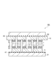
- FIG. 1 is a schematic cross-sectional view showing an embodiment of a thermoelectric conversion module.
- the thermoelectric conversion module 101 shown in FIG. 1 includes opposing high (low) heat side heat sources 21 and low (high) heat side heat sources 22, and a plurality of p-types arranged between them and arranged separately from each other.
- a thermoelectric semiconductor part comprising the semiconductor 1 and a plurality of n-type semiconductors 2 and electrodes 11 and 12 joined by junctions 31 and 32 on both ends of the p-type semiconductor 1 and the n-type semiconductor 2 are provided.
- the p-type semiconductor 1 and the n-type semiconductor 2 are alternately arranged and connected in series by the electrodes 11 and 12.
- a metal diffusion prevention layer 33 is provided on the bonding surface of the p-type semiconductor 1 and the n-type semiconductor 2.
- the high (low) temperature side insulating layer 41 is located between the high (low) temperature side heat source 21 and the electrode 11 and between the low (high) temperature side heat source 22 and the electrode 12. And a low (high) temperature side insulating layer 42 is provided. Note that the installation range of the insulating layer may be either the entire heat source or only the portion in contact with the electrode.
- Examples of the material of the electrodes 11 and 12 include copper, aluminum, nickel, molybdenum, titanium, stainless steel, gold, silver, platinum and the like from the viewpoints of thermal conductivity and conductivity.
- the electrodes 11 and 12 it is preferable to provide a metallized layer on the bonding surface with the bonding portions 31 and 32.
- the material of the metallized layer include nickel, gold, silver, titanium, tungsten, molybdenum and the like.
- the metallized layer can be formed, for example, by a method such as plating, sputtering or vapor deposition.
- the thickness of the metallized layer can be 0.05 ⁇ m to 500 ⁇ m.
- the p-type semiconductor 1 and the n-type semiconductor 2 for example, silicon-germanium type, magnesium-silicon type, manganese-silicon type, bismuth-tellurium type, lead-tellurium type, iron-vanadium-aluminum type, cobalt-antimony type Etc.
- the metal diffusion prevention layer 33 is preferably made of, for example, Ni, Mo, Ti, TiN, Al or the like.
- the thickness of the metal diffusion prevention layer 33 can be 0.01 ⁇ m to 100 ⁇ m.
- thermoelectric conversion module includes the low (high) high temperature heat source 22 and the low (high) high temperature insulation layer between the high (low) high temperature heat source 21 and the high (low) high temperature insulation layer 41.
- a buffer layer is provided on at least one of them.
- the buffer layer is preferably in the form of a sheet from the viewpoint of processability.
- a grease-like one can also be used.
- the material of the sheet-like buffer layer those capable of plastic deformation or elastic deformation between the high (low) heat side heat source 21 or the low (high) heat side heat source 22 and the electrodes 11, 12; What has is preferable.
- gum are mentioned, for example.
- the insulating layer 41 is interposed between the high (low) heat side heat source 21 or the low (high) heat side heat source 22 in contact with the buffer layer or between the electrodes 11 and 12 (42) may not be provided.
- thermoelectric conversion module when used at a low temperature of 200 ° C. or less as the heat source, it is also possible to use a resin film such as a polyimide film, a polyimide tape, or a polytetrafluoroethylene sheet, or a tape.
- a resin film such as a polyimide film, a polyimide tape, or a polytetrafluoroethylene sheet, or a tape.
- the material of the metal fiber and the porous body is preferably made of copper, aluminum, nickel, molybdenum or the like which has high heat conductivity and is easily deformed.
- the electrode 11 and the p-type semiconductor 1 and the n-type semiconductor 2, and the junctions 31 and 32 provided between the electrode 12 and at least one of the p-type semiconductor 1 and the n-type semiconductor 2 It comprises a sintered body of a bonding material (copper paste) containing copper particles. Details of the bonding material (copper paste) will be described later.
- a bonding material is applied to the bonding position of the electrode 11 to the p-type semiconductor 1 and the n-type semiconductor 2 or the bonding surface of the p-type semiconductor 1 and the n-type semiconductor 2 Can be formed by bringing the electrode or the p-type semiconductor and the n-type semiconductor into contact with the coating film provided by drying using a jig if necessary, and baking this coating film (bonding layer) .
- the printing dimension is preferably printed in an area of 80% or more and 120% or less with respect to the area of the end face.
- the thickness of the coating film may be 1 ⁇ m to 1000 ⁇ m, may be 10 ⁇ m to 1000 ⁇ m, may be 10 ⁇ m to 500 ⁇ m, may be 50 ⁇ m to 200 ⁇ m, and is 10 ⁇ m to 3000 ⁇ m. May be 15 ⁇ m to 500 ⁇ m, may be 20 ⁇ m to 300 ⁇ m, may be 5 ⁇ m to 500 ⁇ m, may be 10 ⁇ m to 250 ⁇ m, and may be 15 ⁇ m to 150 ⁇ m. It may be
- the stress relaxation effect, the effect of absorbing the variation in the length of the thermoelectric semiconductor or the variation in the distance between the electrodes, and the printing accuracy are preferably 10 ⁇ m to 1000 ⁇ m. It becomes easy to acquire a stress relaxation effect as the thickness of a coating film is 10 micrometers or more, and it becomes easy to secure printing accuracy as it is 1000 micrometers or less.
- the method of drying the coating film may be drying by standing at normal temperature, heating drying, or drying under reduced pressure.
- heat drying or reduced pressure drying for example, a hot plate, a hot air dryer, a hot air heater, a nitrogen dryer, an infrared dryer, an infrared heater, a far infrared heater, a microwave heater, a laser heater, an electromagnetic A heating device, a heater heating device, a steam heating furnace, a hot plate press device or the like can be used.
- the temperature and time of drying may be appropriately adjusted according to the type and amount of dispersion medium used.
- the drying temperature and time may be, for example, drying at 50 ° C. or more and 180 ° C. or less for 1 minute or more and 120 minutes or less.
- Sintering of the coating film (bonding layer) can be carried out by heat treatment.
- heat treatment for example, a hot plate, a warm air dryer, a warm air heater, a nitrogen dryer, an infrared dryer, an infrared heater, a far infrared heater, a microwave heater, a laser heater, an electromagnetic heater, A heater heating device, a steam heating furnace or the like can be used.
- the gas atmosphere at the time of sintering may be an oxygen-free atmosphere from the viewpoint of oxidation suppression.
- the gas atmosphere at the time of sintering may be a reducing atmosphere from the viewpoint of removing the surface oxide of the copper particles.
- the oxygen-free atmosphere include the introduction of an oxygen-free gas such as nitrogen and a rare gas, or under vacuum.
- a reducing atmosphere for example, in pure hydrogen gas, in a mixed gas of hydrogen and nitrogen represented by forming gas, in nitrogen containing formic acid gas, in a mixed gas of hydrogen and noble gas, in rare gas containing formic acid gas, etc. It can be mentioned.
- the maximum temperature reached during the heat treatment may be 200 ° C. or more and 450 ° C. or less, and 250 ° C. or more and 450 ° C. or less from the viewpoint of reducing the thermal damage to members constituting the thermoelectric conversion module and improving the yield.
- the temperature may be 250 ° C. or more and 400 ° C. or less, or 250 ° C. or more and 350 ° C. or less. If the ultimate maximum temperature is 200 ° C. or higher, sintering tends to proceed sufficiently in the ultimate maximum temperature holding time of 60 minutes or less.
- a bonding material containing a specific amount of a specific additive described later sufficient bonding strength can be obtained even when the ultimate maximum temperature is 250 ° C. or less, preferably 225 ° C. or less.
- the maximum temperature holding time to be reached may be 1 minute or more and 60 minutes or less, or 1 minute or more and less than 40 minutes, or 1 minute More than 30 minutes may be sufficient.
- heating is performed at 350 ° C. or less in hydrogen with a concentration of 1% or more from the viewpoint of the reducibility of the bonding material mainly composed of copper nanoparticles and the reduction of the thermal stress generated between the electrode and the thermoelectric semiconductor. It is preferable to do.
- the coating can be sintered under a load of 0 to 100 MPa.
- bonding can be performed without pressure.
- pressureless means a state in which a pressure of 0.01 MPa or less is received in addition to the weight of the members to be joined or the weight thereof.
- a bonding material contains metal particles and a dispersion medium, and the metal particles have submicro copper particles having a volume average particle diameter of 0.01 ⁇ m to 0.8 ⁇ m and a volume average particle diameter of 2.0 ⁇ m.
- the total of the content of the sub-micro copper particles and the content of the micro copper particles is 80% by mass or more based on the total mass of the metal particles, containing the micro copper particles having a size of 50 ⁇ m or more and 80% by mass or more.
- Content is 30% by mass or more and 90% by mass or less based on the total of the mass of the sub-micro copper particles and the mass of the micro copper particles, and the content of the micro copper particles is based on the total mass of all the metal particles In the case of 10% by mass or more and 50% by mass or less, sufficient bonding strength can be obtained even when bonding is performed without pressure.
- the above-mentioned reason is attributed to the surface protective agent or the dispersion medium while maintaining sufficient sinterability by containing the sub-micro copper particles and the micro copper particles contained in the bonding material in a specific ratio. It is possible that the volume contraction at the time of sintering can be sufficiently suppressed, and securing of the strength of the sintered body and improvement of the bonding strength with the adherend surface can be achieved.
- the above-mentioned bonding material can obtain the above-mentioned effect by submicro copper particles and micro copper particles, compared with the bonding material which has expensive copper nanoparticles as a main component, it is cheaper and stably. It has the advantage of being able to supply.
- the micro copper particles are preferably in the form of flakes.
- the use of the flake-like micro copper particles makes it easier to reduce the thermal stress generated between the electrode and the thermoelectric semiconductor.
- the micro copper particles in the bonding material being oriented substantially parallel to the bonding surface, it is possible to suppress the volume contraction when the bonding material is sintered, flakes It is considered that the bonding strength is improved by increasing the overlapping area of the micro copper particles in the form of a circle, and that the flake-like micro copper particles align the sub-micro copper particles to obtain a reinforcing effect.
- the bonding material (copper paste) after bonding becomes a sintered body (porous body) of copper.
- thermoelectric conversion module is formed in one bonding step. It can also be done.
- one of the bonding portions 31 and 32 is formed using a bonding material such as a brazing material or solder, that is, one of the electrodes 11 and 12 and the p-type semiconductor 1 and the n-type semiconductor 2 is a brazing material or
- a bonding step of bonding with a brazing material or solder can be performed first, and then a bonding step of bonding with a bonding material containing copper particles can be performed.
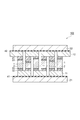
- FIG. 2 is a schematic cross-sectional view showing another embodiment of the thermoelectric conversion module.
- the lengths in the current direction of the p-type semiconductor 1 and the n-type semiconductor 2, which are thermoelectric semiconductors are dispersed. .
- the lengths of the p-type semiconductor 1 and the n-type semiconductor 2 in the current direction are the same for the p-type semiconductor 1 and the n-type semiconductor 2 in which the electrode 11 is located below and joined or disposed on the electrode 11 It can also be referred to as the variation in height, and it can also be referred to as the variation in position of the bonding surface on the electrode 12 side.
- the p-type semiconductor 1 and the p-type semiconductor 1 are manufactured similarly to the first embodiment.
- a bonding material containing copper particles is applied to the bonding surface of the n-type semiconductor 2 or the bonding position with the p-type semiconductor 1 and the n-type semiconductor 2 in the other of the electrodes 11 and 12, and the second bonding step is performed be able to.
- the second bonding step it is preferable to press the other of the electrodes 11 and 12 and the p-type semiconductor 1 and the n-type semiconductor 2 in directions approaching each other and thereafter bake the bonding layer.
- the firing may be performed while pressing the other of the electrodes 11 and 12 and the p-type semiconductor 1 and the n-type semiconductor 2 in directions approaching each other.
- the p-type semiconductor 1 and the n-type semiconductor 2 can be formed by the bonding layer having shape following property. Adhesion to the other of the electrodes 11 and 12 can be sufficiently obtained. Moreover, the height variation of the thermoelectric conversion module after joining can be reduced.
- thermoelectric conversion module when the variation in the length of the p-type semiconductor 1 and the n-type semiconductor 2 is 30 ⁇ m or more, it is easy to adjust the height of the thermoelectric conversion module within a predetermined range by performing the second bonding step. Thus, the cost of the thermoelectric conversion module can be reduced.
- the variation in the length of the p-type semiconductor 1 and the n-type semiconductor 2 is preferably 200 ⁇ m or less from the viewpoint of processing accuracy and shape retention of the bonding portion 31.
- the variation in lengths of the p-type semiconductor 1 and the n-type semiconductor 2 may be 10 to 200 ⁇ m, 100 to 200 ⁇ m, 10 to 50 ⁇ m, or 50 to 100 ⁇ m. Good.
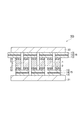
- FIG. 3 is a schematic cross-sectional view showing another embodiment of the thermoelectric conversion module.
- the electrodes in the thermoelectric conversion module of FIGS. 1 and 2 are changed to electrodes 15 and 16 with insulating layers, and the high (low) heat side insulating layer 41 and the low (high) temperature It has the component same as the said 1st embodiment and the said 2nd embodiment except the side insulating layer 42 being not provided. That is, also in the present embodiment, the lengths of the p-type semiconductor 1 and the n-type semiconductor 2 may have variations.
- the thermoelectric conversion module 103 includes the electrodes 15 and 16 with the insulating layer, so that the high (low) temperature side insulating layer 41 and the low (high) temperature side insulating layer 42 shown in the first embodiment are provided. Can be omitted, and the structure of the thermoelectric conversion module can be simplified.
- the electrodes 15 and 16 with an insulating layer those having a laminated structure in which the insulating layer 14 is sandwiched between the conductive layers 13 can be mentioned.
- the material of the conductive layer 13 include copper, aluminum, nickel, and molybdenum.
- the material of the insulating layer 14 may be ceramic, resin, glass or the like, and ceramic is preferable from the viewpoint of heat resistance and contact thermal resistance.
- the bonding material of the present embodiment contains metal particles and a dispersion medium.
- the metal particles include copper particles and metal particles other than copper particles.
- the copper particles include sub-micro copper particles and micro copper particles.
- the sub-micro copper particles refer to copper particles having a particle size of 0.01 ⁇ m or more and less than 1.00 ⁇ m.
- the micro copper particles refer to copper particles having a particle size of 1 ⁇ m or more and less than 50 ⁇ m.
- the particle size of the copper particles can be determined by the following method.
- the particle size of the copper particles can be calculated, for example, from an SEM image.
- the powder of copper particles is placed on a carbon tape for SEM with a spatula to make a sample for SEM. This SEM sample is observed at 5000 ⁇ with a SEM apparatus.
- a quadrangle circumscribed to the copper particles of this SEM image is drawn by image processing software, and one side thereof is taken as the particle diameter of the particles.
- sub-micro copper particles examples include those containing copper particles having a particle diameter of 0.12 ⁇ m or more and 0.8 ⁇ m or less, and, for example, using copper particles having a volume average particle diameter of 0.12 ⁇ m or more and 0.8 ⁇ m or less it can. If the volume average particle size of the submicro copper particles is 0.12 ⁇ m or more, effects such as suppression of the synthesis cost of the submicro copper particles, good dispersibility, and suppression of the amount of the surface treatment agent can be easily obtained. If the volume average particle size of the submicro copper particles is 0.8 ⁇ m or less, the effect of excellent sintering properties of the submicro copper particles is easily obtained.
- the volume average particle diameter of the sub-micro copper particles may be 0.15 ⁇ m or more and 0.8 ⁇ m or less, or 0.15 ⁇ m or more and 0.6 ⁇ m or less, or 0 It may be 0.2 ⁇ m or more and 0.5 ⁇ m or less, and may be 0.3 ⁇ m or more and 0.45 ⁇ m or less.
- the volume average particle size means 50% volume average particle size.
- SALD-7500 nano, Shimadzu Corporation make Shimadzu nanoparticle distribution measurement apparatus
- hexane, toluene, ⁇ -terpineol or the like can be used as a dispersion medium.
- the sub-micro copper particles can contain 10% by mass or more of copper particles having a particle diameter of 0.12 ⁇ m to 0.8 ⁇ m. From the viewpoint of the sinterability of the bonding material, the sub-micro copper particles can contain 20 mass% or more, 30 mass% or more of copper particles with a particle size of 0.12 ⁇ m or more and 0.8 ⁇ m or less, 100 It can contain mass%.
- the dispersibility of a copper particle improves more that the content rate of the copper particle whose particle size in a submicro copper particle is 0.12 micrometer or more and 0.8 micrometer or less is 20 mass% or more, a raise of a viscosity, and the fall of paste concentration It can suppress more.
- the content of the sub-micro copper particles may be 20% by mass or more and 90% by mass or less, 30% by mass or more and 90% by mass or less, 35% by mass or more, based on the total mass of the metal particles. 85 mass% or less may be sufficient, and 40 mass% or more and 80 mass% or less may be sufficient. If the content of the sub-micro copper particles is within the above range, it becomes easy to form the bonding portion according to the present embodiment described above.
- the bonding material of the present embodiment includes sub-micro copper particles and flaky micro copper particles as copper particles
- the content of the sub-micro copper particles is the mass of sub-micro copper particles and flaky micro copper particles. 20 mass% or more and 90 mass% or less may be sufficient based on the sum total of mass. If the content of the sub-micro copper particles is 20% by mass or more, the flake-like micro copper particles can be sufficiently filled, and it becomes easy to form the bonding portion according to the above-described embodiment. . If the content of the sub-micro copper particles is 90% by mass or less, the volume contraction can be sufficiently suppressed when the bonding material is sintered, so that it is easy to form the bonding portion according to the above-described embodiment. Become.
- the content of the sub-micro copper particles is 30% by mass or more and 85% by mass or less based on the total of the mass of the sub-micro copper particles and the mass of the flaky micro copper particles And may be 35% by mass or more and 85% by mass or 40% by mass or more and 80% by mass or less.
- the shape of the sub-micro copper particles is not particularly limited.
- Examples of the shape of the sub-micro copper particles include spherical, massive, needle-like, flake-like, substantially spherical and aggregates thereof.
- the shape of the sub-micro copper particles may be spherical, substantially spherical, or flake-like, and from the viewpoint of combustibility, dispersibility, mixing with flake-like micro copper particles, etc. It may be spherical or substantially spherical.
- the submicro copper particles may have an aspect ratio of 5 or less or 3 or less from the viewpoint of dispersibility, filling property, and miscibility with the flake-like micro copper particles.
- aspect ratio indicates the long side / thickness of particles. The measurement of the long side and the thickness of the particle can be determined, for example, from the SEM image of the particle.
- the sub-micro copper particles may be treated with a specific surface treatment agent.
- Specific surface treatment agents include, for example, organic acids having 8 to 16 carbon atoms. Examples of the organic acid having 8 to 16 carbon atoms include caprylic acid, methylheptanoic acid, ethylhexanoic acid, propylpentanoic acid, pelargonic acid, methyloctanoic acid, ethylheptanoic acid, propylhexanoic acid, capric acid, methylnonanoic acid, ethyl Octanoic acid, propyl heptanoic acid, butyl hexanoic acid, undecanoic acid, methyl decanoic acid, ethyl nonanoic acid, propyl octanoic acid, butyl heptanoic acid, lauric acid, methyl undecanoic acid, ethyl decanoic acid, propyl nonanoic acid,
- An organic acid may be used individually by 1 type, and may be used in combination of 2 or more type. By combining such an organic acid and the above-described sub-micro copper particles, the dispersibility of the sub-micro copper particles tends to be compatible with the releasability of the organic acid at the time of sintering.
- the specific surface area of the submicro copper particles can be calculated by measuring the dried submicro copper particles by a BET specific surface area measurement method.
- Minimum coverage of the surface treatment agent if the surface treatment agent is a straight-chain saturated fatty acids, is 2.05 ⁇ 10 -19 m 2/1 molecule.
- calculation from a molecular model or “chemistry and education” Kohiro Ueda, Sumio Inafuku, Morishima, 40 (2), 1992, p 114-117) It can measure by the method of a statement. An example of the quantification method of a surface treating agent is shown.
- the surface treatment agent can be identified by the thermal desorption gas / gas chromatography mass spectrometer of the dry powder obtained by removing the dispersion medium from the bonding material, whereby the carbon number and the molecular weight of the surface treatment agent can be determined.
- the carbon content of the surface treatment agent can be analyzed by carbon content analysis.
- a carbon content analysis method a high frequency induction furnace combustion / infrared absorption method is mentioned, for example.
- the amount of surface treatment agent can be calculated by the above equation from the carbon number, molecular weight and carbon content ratio of the identified surface treatment agent.
- the above-mentioned processing amount of a surface treating agent may be 0.07 mass% or more and 2.1 mass% or less, may be 0.10 mass% or more and 1.6 mass% or less, 0.2 mass% More than 1.1 mass% may be sufficient.
- a commercially available thing can be used as a submicro copper particle.
- sub-micro copper particles for example, CH-0200 (manufactured by Mitsui Mining & Smelting Co., Ltd., volume average particle diameter 0.36 ⁇ m), HT-14 (manufactured by Mitsui Mining & Smelting Co., Ltd., volume average particle diameter 0. 41 ⁇ m), CT-500 (manufactured by Mitsui Mining & Smelting Co., Ltd., volume average particle diameter 0.72 ⁇ m), Tn-Cu 100 (manufactured by Taiyo Nichi acid Co., Ltd., volume average particle diameter 0.12 ⁇ m).
- micro copper particles examples include those containing copper particles having a particle diameter of 1.0 ⁇ m to 50 ⁇ m.
- copper particles having a volume average particle diameter of 1.0 ⁇ m to 50 ⁇ m can be used.
- the volume average particle size of the micro copper particles may be 2.0 ⁇ m or more and 20 ⁇ m or less, may be 2.0 ⁇ m or more and 10 ⁇ m or less, 3.0 ⁇ m or more and 20 ⁇ m or less, and 3.0 ⁇ m or more It may be up to 10 ⁇ m or less.
- micro copper particles examples include, for example, spheres, lumps, needles, flakes, substantially spheres, and aggregates thereof.
- flake shape is preferable.
- flake shape includes flat shapes, such as plate shape and scale shape.
- the flake-like micro copper particles include those containing copper particles having a maximum diameter of 1 ⁇ m to 20 ⁇ m and an aspect ratio of 4 or more, and, for example, an average maximum diameter of 1 ⁇ m to 20 ⁇ m and an aspect ratio of 4
- the above copper particles can be used. If the mean maximum diameter and aspect ratio of the flake-like micro copper particles are within the above range, the volume contraction at the time of sintering the bonding material can be sufficiently reduced, and the bonding portion according to the present embodiment described above can be formed. It becomes easy. From the viewpoint of achieving the above-mentioned effect more, the average maximum diameter of the flake-like micro copper particles may be 1 ⁇ m to 10 ⁇ m, or 3 ⁇ m to 10 ⁇ m.
- the measurement of the maximum diameter and the average maximum diameter of the flake-like micro copper particles can be determined, for example, from a SEM image of the particles, and determined as the major axis X of the flaky structure described later and the average value X av of the major axes.
- the flaky micro copper particles can contain 50% by mass or more of copper particles having a maximum diameter of 1 ⁇ m or more and 20 ⁇ m or less.
- the flake-like micro copper particles can contain 70% by mass or more and 80% by mass or more of copper particles having a maximum diameter of 1 ⁇ m or more and 20 ⁇ m or less, from the viewpoint of orientation in a joined body, reinforcing effect, and filling property of bonding paste. It can be 100% by mass. From the viewpoint of suppressing the bonding failure, it is preferable that the flaky micro copper particles do not contain particles having a size larger than the bonding thickness, such as particles having a maximum diameter of more than 20 ⁇ m, for example.
- the method of calculating the major axis X of flaky micro copper particles from a SEM image is illustrated.
- the powder of flaky micro copper particles is placed on a carbon tape for SEM with a spatula to make a sample for SEM.
- This SEM sample is observed at 5000 ⁇ with a SEM apparatus.
- a rectangle circumscribing the flaky micro copper particles of the SEM image is drawn by image processing software, and the long side of the rectangle is taken as the major axis X of the particle.
- This measurement is performed on 50 or more flake-like micro copper particles using a plurality of SEM images, and the average value Xav of the major axis is calculated.
- the flake-like micro copper particles may have an aspect ratio of 4 or more, or 6 or more. If the aspect ratio is within the above range, the volumetric shrinkage when the bonding layer (bonding material) is sintered can be achieved by the flaky micro copper particles in the bonding material being oriented substantially parallel to the bonding surface. This can be suppressed, and it becomes easy to form the joint according to the above-described embodiment.
- the shape of the flake-like micro copper particles according to the present embodiment can also be defined by the parameters of long diameter (average maximum diameter) X, medium diameter (width) Y, and short diameter (thickness) T.
- the major axis X is a distance between two parallel planes selected so that the distance between the two parallel planes is the largest among the parallel two planes circumscribed to the flake-like micro copper particles in the three-dimensional shape of the flake-like micro copper particles is there.
- Medium diameter Y is orthogonal to parallel two planes giving major axis X, and among parallel two planes circumscribed to flake-like micro copper particles, parallel two planes selected so as to maximize the distance between these parallel two planes Distance.
- the minor diameter T is orthogonal to the parallel two planes giving the major axis X and the parallel two planes giving the medium diameter Y, and the distance between the parallel two planes of the parallel two planes circumscribed to the flaky micro copper particles is the largest.
- the mean value Xav of the major axis may be 1 ⁇ m to 50.0 ⁇ m, may be 1 ⁇ m to 20 ⁇ m, or may be 3 ⁇ m to 10 ⁇ m. If Xav is within the above range, it is easy to form a sintered body of the bonding material with an appropriate thickness in a bonded body manufactured by sintering the bonding material.
- the ratio (aspect ratio) of the ratio (averaged aspect ratio) of the average value Xav of the major axis to the average value Tav of the minor axis may be 4.0 or more, or 6.0 or more, and 10.0 or more It may be. If Xav / Tav is in the above range, the flake-like micro copper particles in the bonding material can be easily oriented substantially parallel to the bonding surface, and the volume contraction can be suppressed when the bonding material is sintered, It becomes easy to secure the bonding strength of the bonded body manufactured by sintering the bonding material. When the bonding material is used to bond the thermoelectric semiconductor and the electrode in the thermoelectric conversion module, the bonding strength and connection reliability of the thermoelectric conversion module can be easily improved.
- the ratio Xav / Yav which is the ratio of the mean value Xav of the major diameter to the mean value Yav of the median diameter, may be 2.0 or less, 1.7 or less, or 1.5 or less. . If Xav / Yav is within the above range, the flake-like micro copper particles become flake-like particles having a certain area, and the flake-like micro copper particles in the bonding material are oriented substantially parallel to the bonding surface It becomes easy, it can control the volume contraction at the time of sintering a joining material, and it becomes easy to secure the junction intensity of the joined object manufactured by sintering a joining material.
- thermoelectric conversion module When the bonding material is used to bond the thermoelectric semiconductor and the electrode in the thermoelectric conversion module, the bonding strength and connection reliability of the thermoelectric conversion module can be easily improved.
- Xav / Yav exceeds 2.0, it means that the shape of the flaky micro copper particles approaches an elongated linear shape.
- the ratio Yav / Tav which is the ratio of the mean value Yav of the medium diameter to the mean value Tav of the short diameter, may be 2.5 or more, may be 4.0 or more, or even 8.0 or more. Good.
- Yav / Tav is in the above range, the flake-like micro copper particles in the bonding material can be easily oriented substantially parallel to the bonding surface, and the volume contraction when the bonding material is sintered can be suppressed. It becomes easy to secure the bonding strength of the bonded body manufactured by sintering the bonding material.
- the bonding material is used to bond the thermoelectric semiconductor and the electrode in the thermoelectric conversion module, the bonding strength and connection reliability of the thermoelectric conversion module can be easily improved.
- the content of the flaky micro copper particles may be 1% by mass or more and 90% by mass or less, 10% by mass or more and 70% by mass, or 20% by mass, based on the total mass of the metal particles. More than 50 mass% may be sufficient. When the content of the flaky micro copper particles is within the above range, it becomes easy to form the bonding portion according to the above-described embodiment.
- the total content of sub-micro copper particles and the content of flaky micro copper particles is the total of metal particles. 80 mass% or more may be sufficient on the basis of mass. If the sum of the content of the submicro copper particles and the content of the flaky micro copper particles is within the above range, it becomes easy to form the bonding portion according to the present embodiment described above. From the viewpoint of achieving the above effect, the total content of the sub-micro copper particles and the content of the flaky micro copper particles may be 90% by mass or more based on the total mass of the metal particles, 95 It may be mass% or more, and may be 100 mass%.
- the presence or absence of the treatment of the surface treatment agent is not particularly limited.
- the flake-like micro copper particles may be treated with a surface treatment agent.
- the surface treatment agent may be removed at the time of bonding.
- Such surface treatment agents include aliphatic carboxylic acids such as palmitic acid, stearic acid, arachidic acid and oleic acid; aromatic carboxylic acids such as terephthalic acid, pyromellitic acid and o-phenoxybenzoic acid; cetyl alcohol Aliphatic alcohols such as stearyl alcohol, isobornyl cyclohexanol and tetraethylene glycol; aromatic alcohols such as p-phenylphenol; alkyl amines such as octylamine, dodecylamine and stearylamine; stearonitrile, decanenitrile and the like Aliphatic nitriles; silane coupling agents such as alkyl alkoxysilanes; and polymer processing agents such as polyethylene glycol, polyvinyl alcohol, polyvinyl pyrrolidone, silicone oligomers and the like.
- a surface treatment agent may be used individually by 1 type, and may be used in combination of 2 or more
- the treatment amount of the surface treatment agent may be an amount of one or more molecular layers on the particle surface.
- the throughput of such a surface treatment agent varies depending on the specific surface area of the flaky micro copper particles, the molecular weight of the surface treatment agent, and the minimum coverage area of the surface treatment agent.
- the treatment amount of the surface treatment agent is usually 0.001% by mass or more.
- the specific surface area of the flaky micro copper particles, the molecular weight of the surface treatment agent, and the minimum coverage area of the surface treatment agent can be calculated by the method described above.
- the bonding material is prepared only from the above-mentioned sub-micro copper particles, the volume shrinkage and sintering shrinkage accompanying the drying of the dispersion medium are large, so it becomes easy to separate from the adherend surface during sintering of the bonding material and bonding of thermoelectric semiconductors etc. In this case, it is difficult to obtain sufficient bonding and reliability.
- the sub-micro copper particles and the flaky micro copper particles in combination, the volume contraction when the bonding material is sintered is suppressed, and it becomes easy to form the bonding portion according to the above-described embodiment.
- the content of the micro copper particles having a maximum diameter of 1 ⁇ m to 20 ⁇ m and an aspect ratio of less than 2 contained in the metal particles is a maximum diameter of 1 ⁇ m to 20 ⁇ m, and the aspect ratio 50 mass% or less is preferable on the basis of 4 or more flaky micro copper particle whole quantity, and it is more preferable to set it as 30 mass% or less.
- the flaky micro copper particles in the bonding material are oriented substantially parallel to the bonding surface It becomes easy and it can control more effectively volume contraction when sintering a jointing material.
- the content of the micro copper particles having an average maximum diameter of 1 ⁇ m or more and 20 ⁇ m or less and an aspect ratio of less than 2 is 1 ⁇ m or more and 20 ⁇ m or less in that such effects can be further easily obtained.
- 20 mass% or less may be 10 mass% or less on the basis of 4 or more flaky micro copper particle whole quantity.
- flake shaped micro copper particle which concerns on this embodiment.
- examples of commercially available flake-like micro copper particles include MA-C025 (manufactured by Mitsui Mining & Smelting Co., Ltd., average maximum diameter 4.1 ⁇ m), 3L3 (manufactured by Fukuda Metal Foil & Powder Industry Co., Ltd., maximum volume diameter 7.3 ⁇ m). 1110F (manufactured by Mitsui Mining & Smelting Co., Ltd., average maximum diameter 5.8 ⁇ m), 2L3 (manufactured by Fukuda Metal Foil & Powder Co., Ltd., average maximum diameter 9 ⁇ m).
- the micro copper particles to be blended include flake-like micro copper particles having a maximum diameter of 1 ⁇ m to 20 ⁇ m and an aspect ratio of 4 or more, and a maximum diameter of 1 ⁇ m to 20 ⁇ m. It is possible to use micro copper particles in which the content of micro copper particles having an aspect ratio of less than 2 is 50% by mass or less, preferably 30% by mass or less, based on the total amount of the flake-like micro copper particles.
- flake-like micro copper particles which are commercially available, they contain flake-like micro copper particles having a maximum diameter of 1 ⁇ m to 20 ⁇ m and an aspect ratio of 4 or more, and a maximum diameter of 1 ⁇ m to 20 ⁇ m,
- the content of the micro copper particles having a ratio of less than 2 may be selected to be 50% by mass or less, preferably 30% by mass or less, based on the total amount of the flake-like micro copper particles.
- the metal particles may contain other metal particles other than the above-described sub-micro copper particles and micro copper particles, and may contain, for example, particles of zinc, nickel, silver, gold, palladium, platinum, etc. .
- the other metal particles may have a volume average particle diameter of 0.01 ⁇ m to 10 ⁇ m, may be 0.01 ⁇ m to 5 ⁇ m, or may be 0.05 ⁇ m to 3 ⁇ m.
- the content may be less than 20% by mass and not more than 10% by mass based on the total mass of the metal particles from the viewpoint of obtaining sufficient bondability. May be Other metal particles may not be included.
- the shape of the other metal particles is not particularly limited.
- the bonding material of the present embodiment includes metal particles other than copper particles, it is possible to obtain a sintered metal layer in which a plurality of metals are dissolved or dispersed in a solid solution. Characteristics are improved and connection reliability is likely to be improved. In addition, by adding a plurality of types of metal particles, the bonding portion formed can easily improve bonding strength and connection reliability with respect to an adherend such as a thermoelectric semiconductor and an electrode.
- the dispersion medium is not particularly limited, and may be volatile.
- volatile dispersion media include pentanol, hexanol, heptanol, octanol, decanol, ethylene glycol, diethylene glycol, propylene glycol, butylene glycol, ⁇ -terpineol, isobornyl cyclohexanol (MTPH), etc.
- Alcohols ethylene glycol butyl ether, ethylene glycol phenyl ether, diethylene glycol methyl ether, diethylene glycol ethyl ether, diethylene glycol butyl ether, diethylene glycol isobutyl ether, diethylene glycol hexyl ether, triethylene glycol methyl ether, diethylene glycol dimethyl ether, diethylene glycol diethyl ether, diethylene glycol Butyl ether, diethylene glycol butyl methyl ether, diethylene glycol isopropyl methyl ether, triethylene glycol dimethyl ether, triethylene glycol butyl methyl ether, propylene glycol propyl ether, dipropylene glycol methyl ether, dipropylene glycol ethyl ether, dipropylene glycol propyl ether, dipropylene glycol propyl ether Ethers such as butyl ether, dipropylene glycol dimethyl ether, tripropylene glycol methyl
- Examples of mercaptans having an alkyl group having 1 to 18 carbon atoms include ethyl mercaptan, n-propyl mercaptan, i-propyl mercaptan, n-butyl mercaptan, i-butyl mercaptan, t-butyl mercaptan, pentyl mercaptan and hexyl mercaptan And dodecyl mercaptan.
- Examples of mercaptans having a cycloalkyl group having 5 to 7 carbon atoms include cyclopentyl mercaptan, cyclohexyl mercaptan and cycloheptyl mercaptan.
- the content of the dispersion medium may be 5 to 50 parts by mass based on 100 parts by mass of the total mass of the metal particles. If the content of the dispersion medium is within the above range, the bonding material can be adjusted to a more appropriate viscosity, and sintering of the copper particles is less likely to be inhibited.
- the dispersion medium preferably contains a solvent having a boiling point of 300 ° C. or higher.
- the boiling point of the solvent having a boiling point of 300 ° C. or higher is 300 ° C. from the viewpoint of rapid evaporation / removal when the bonding temperature is reached without hindering sintering and densification.
- the temperature may be 450 ° C. or less, 305 ° C. to 400 ° C., or 310 ° C. to 380 ° C.
- the solvent having a boiling point of 300 ° C. or higher is preferably selected to have a structure having high affinity to the metal particle surface in order to improve the dispersibility of the contained metal particles.
- a solvent having an alkyl group As a solvent having such a boiling point of 300 ° C.
- a solvent having a boiling point of 300 ° C. or higher is selected from the group consisting of a hydroxy group, an ether group, and an ester group because an organic acid, an organic amine, a hydroxyl group-containing polymer, polyvinyl pyrrolidone and the like are easy to handle as a surface treatment agent. It is preferable to have at least one kind of group.
- the Hansen solubility parameter can be retrieved, for example, from the end database of the following published document, or retrieved / calculated by the database and simulation integrated software HSPiP. Open literature: "HANSEN SOLUBILITY PARAMETERS: A USER'S HANDBOOK" (CRC Press, 1999)
- the content of the solvent having a boiling point of 300 ° C. or more can be 2% by mass or more based on the total mass of the bonding material.
- the content of the solvent having a boiling point of 300 ° C. or more may be 2.2% by mass or more, or 2.4% by mass or more based on the total mass of the bonding material. If the content of the solvent having a boiling point of 300 ° C. or more falls within the above range, a certain amount of solvent can remain in the bonding layer when sintering the bonding layer of the present embodiment, and between the members The flexibility and adhesion of the bonding material are easily maintained, and even when the members used for bonding have different thermal expansion coefficients, bonding tends to be possible without peeling.
- the upper limit of the content of the solvent having a boiling point of 300 ° C. or higher is not particularly limited. From the viewpoint of shortening the time until the dispersion medium is removed at the sintering temperature and shortening the sintering time, it may be 9% by mass or less based on the total mass of the bonding material.
- the content of the solvent having a boiling point of 300 ° C. or more may be 15% by volume or more, or 17% by volume or more based on the total volume of the bonding material. It may be 23% by volume or more. If the content of the solvent having a boiling point of 300 ° C. or more falls within the above range, a certain amount of solvent can remain in the bonding layer when sintering the bonding layer of the present embodiment, and between the members The flexibility and adhesion of the bonding material are easily maintained, and even when the members used for bonding have different thermal expansion coefficients, bonding tends to be possible without peeling.
- the upper limit of the content of the solvent having a boiling point of 300 ° C. or higher is not particularly limited. From the viewpoint of suppressing the time until the dispersion medium is removed at the sintering temperature and shortening the sintering time, it may be 60% by volume or less based on the total volume of the bonding material.
- the type of dispersion medium contained in the bonding material can be analyzed by, for example, gas chromatography-mass spectrometry of high temperature desorbed gas, and TOF-SIMS.
- the supernatant obtained by separating the particle components by centrifugation may be identified by ordinary organic analysis such as FT-IR, NMR, liquid chromatograph and a combination thereof.
- the ratio of the type of dispersion medium can be quantified by liquid chromatography, NMR or the like.
- the bonding material if necessary, a monovalent carboxylic acid having 1 to 9 carbon atoms; a wetting improver such as a nonionic surfactant or a fluorinated surfactant; an antifoamer such as silicone oil; inorganic ion exchange You may add ion trap agents etc. of a body etc. suitably.
- the bonding material preferably contains a monovalent carboxylic acid having 1 to 9 carbon atoms in that bonding can be performed at a low temperature of 250 ° C. or less and sufficient bonding strength can be obtained.
- the monovalent carboxylic acid having 1 to 9 carbon atoms is, for example, a carboxylic acid having a hydrocarbon group having 1 to 8 carbon atoms and one carboxyl group.
- the hydrocarbon group may be either a saturated hydrocarbon group or an unsaturated hydrocarbon group, and may be linear, branched or cyclic.
- the monovalent carboxylic acid having 1 to 9 carbon atoms preferably has no hydroxy group.
- Examples of the monovalent carboxylic acid having 1 to 9 carbon atoms include formic acid (CH 2 O 2 ), acetic acid (C 2 H 4 O 2 ), propionic acid or propanoic acid (C 3 H 6 O 2 ), butanoic acid or butyric acid (C 4 H 8 O 2 ), pentanoic acid or valeric acid (C 5 H 10 O 2 ), caproic acid or hexanoic acid (C 6 H 12 O 2 ), 2-methylpentanoic acid or 2-methyl valerate acid (C) 6 H 12 O 2 ), heptanoic acid or enanthate (C 7 H 14 O 2 ), caprylic acid or octanoic acid (C 8 H 16 O 2 ), pelargonic acid or nonanoic acid (C 9 H 18 O 2 ), crotonate Acid (C 4 H 6 O 2 ), methacrylic acid (C 4 H 6 O 2 ), angelica acid (C 5 H 8 O 2 ), tiglic acid
- the content of the monovalent carboxylic acid having 1 to 9 carbon atoms is preferably 0.2% by mass or more based on the total amount of the dispersion medium from the viewpoint of low temperature bonding and bonding strength.
- the content of the monovalent carboxylic acid having 1 to 9 carbon atoms is preferably less than 1.0% by mass, based on the total amount of the dispersion medium, from the viewpoint of storage stability of the bonding material, and 0.9% It is more preferable that the content is less than%.
- the bonding material according to the present embodiment described above is suitable as a bonding material for a thermoelectric conversion module used to bond the thermoelectric semiconductor of the thermoelectric conversion module including the thermoelectric semiconductor and the electrode to the electrode.
- the bonding material may be prepared by mixing the above-described sub-micro copper particles, micro copper particles, other metal particles and optional additives in a dispersion medium. An agitation process may be performed after mixing of each component. The bonding material may adjust the maximum particle size of the dispersion by classification operation.
- sub-micro copper particles, a surface treatment agent, and a dispersion medium are mixed in advance and dispersion treatment is performed to prepare a dispersion liquid of sub-micro copper particles, and further micro copper particles, other metal particles and optional addition
- the agents may be mixed and prepared.
- the bonding portion includes a sintered body of a bonding material according to the present embodiment, which includes copper particles.
- FIG. 4 is an enlarged cross-sectional view of the joint portion according to the present embodiment.
- the bonding portion 31 for bonding the electrode 12 and the thermoelectric semiconductor is a sintered body of a bonding layer including a metal particle and a dispersion medium, and the metal particle is formed of a bonding material including submicro copper particles and micro copper particles.
- the bonding layer formed of the bonding material of the present embodiment described above is heated at 350 ° C. or less in hydrogen at a concentration of 1% or more, and the volume resistivity, the thermal conductivity and the bonding strength are respectively
- a sintered body which is 1 ⁇ 10 ⁇ 5 ⁇ ⁇ cm or less, 50 W ⁇ m ⁇ 1 ⁇ K ⁇ 1 or more and 20 MPa or more can be formed, and the joint portion includes such a sintered body, It is possible to realize a thermoelectric conversion module excellent in power generation performance and thermal stress characteristics.
- ⁇ is the electrical resistivity per unit volume (volume resistivity) ( ⁇ ⁇ m)
- R is the resistance of the sintered body ( ⁇ )
- A is the sectional area of the sintered body (m 2 )
- L is the burning
- the thickness (m) of the body is shown.
- the thermal conductivity can be calculated from the thermal diffusivity, the specific heat capacity, and the density of the joint.
- the thermal diffusivity of the joint is measured by a laser flash method (LFA 467, manufactured by Netti), and this thermal diffusivity, and the specific heat capacity obtained by a differential scanning calorimeter (DSC 8500, manufactured by Perkin Elmer),
- the thermal conductivity [W / (m ⁇ K)] of the joint at 25 ° C. can be calculated by the product of the density and the density obtained in the same manner as described above.
- the bonding strength can be measured using a universal bond tester (4000 series, manufactured by DAGE) or the like. Moreover, it can also measure by the method as described in an Example.
- the bonding portion includes a structure 31 (b) derived from flake-like copper particles oriented substantially parallel to the interface with the electrode, and the copper content in the bonding portion is based on the volume of the bonding portion, 65 volume% or more may be sufficient.
- a flake-like structure in the structure originating in the copper particle of flake-like micro copper particles ie, sintered copper which has flake-like structure
- five or more may be sufficient as a ratio of a major axis and thickness.
- the number average diameter of the major axis of the flake-like structure may be 2 ⁇ m or more, 3 ⁇ m or more, or 4 ⁇ m or more. If the shape of the flake-like structure is in this range, the reinforcing effect by the flake-like structure contained in the bonding portion is improved, and the thermoelectric conversion module becomes more excellent in reliability.
- the major axis and thickness of the flake-like structure can be determined, for example, from the SEM image of the bonded body (the bonding portion and the electrode or the thermoelectric semiconductor).
- the method of measuring the long diameter and thickness of a flaky structure from a SEM image is illustrated.
- the joint is poured so that the entire sample is filled with an epoxy casting resin and cured.
- the cast sample is cut in the vicinity of the cross section to be observed, the cross section is cut by polishing, and CP (cross section polisher) processing is performed.
- the cross section of the sample is observed at 5000 ⁇ with a SEM device.
- a cross-sectional image (for example, 5000 times) of the joined body is acquired, and it is a dense continuous portion, and in a linear, rectangular, or ellipsoidal portion, the maximum length of straight lines included in this portion
- the major axis length is 1 ⁇ m or more
- the major axis / thickness ratio is 4 or more, where the major axis length and the length of the longest straight line included in this portion orthogonal to it are the thickness.
- a certain thing is regarded as a flaky structure, and the major axis and thickness of the flaky structure can be measured by image processing software having a length measuring function. These average values can be obtained by calculating a number average with 20 or more randomly selected points.
- the major axis of the flake-like structure is given as the distance between the parallel straight lines selected so as to maximize the distance between the parallel two straight lines circumscribing the flake-like structure.
- the thickness of the flake-like structure is a distance between two parallel parallel planes which are orthogonal to the parallel two straight lines giving the major axis and which circumscribe the flake like structure and in which the distance between the parallel two planes is maximized. Given.
- the image processing software is not particularly limited, and, for example, Microsoft PowerPoint (manufactured by Microsoft) or ImageJ (manufactured by the National Institutes of Health) can be used.
- the content ratio of the flake-like structure to the entire structure is obtained by determining the cross-sectional area of the joined body from the SEM image of the joined body, and determining the cross-sectional area of the flake-like structure from the major axis and thickness of the flaked structure measured by the above method Can be calculated by dividing the total cross-sectional area of the flake-like structure obtained by summing
- the content ratio of the flake-like structure to the entire structure obtained by the above method may be 10 to 40%, or may be 20 to 30%.
- the content (volume ratio) of copper in the bonding portion can be 65% by volume or more based on the volume of the bonding portion.
- the content of copper in the bonding portion may be 67% by volume or more, or 70% by volume or more based on the volume of the bonding portion. From the viewpoint of easiness of the manufacturing process, the content of copper in the joint may be 90% by volume or less based on the volume of the joint.
- the copper content in the joint can be determined by the following procedure. First, a junction is cut out in a rectangular solid, the longitudinal and lateral lengths of the junction are measured with a caliper or an external shape measuring device, and the thickness is measured with a film thickness meter to calculate the volume of the junction.
- the apparent density M 1 (g / cm 3 ) is determined from the volume of the cut-out joint and the weight of the joint measured by a precision balance.
- acetic acid manufactured by Wako Pure Chemical Industries, Ltd.
- terpineol manufactured by Wako Pure Chemical Industries, Ltd.
- tributyrin manufactured by Wako Pure Chemical Industries, Ltd.
- hexanoic acid made by Wako Pure Chemical Industries, Ltd.
- nonanoic acid made by Wako Pure Chemical Industries, Ltd.
- stearic acid made by Wako Pure Chemical Industries, Ltd.
- tartaric acid made by Wako Pure Chemical Industries, Ltd.
- succinic acid made by Wako Pure Chemical Industries, Ltd.) 2,2-bis (hydroxymethyl) propionic acid (Tokyo Chemical Industry Co., Ltd.), dodecylamine (Wako Pure Chemical Industries, Ltd.), N, N-dimethylformamide (Wako Pure Chemical Industries, Ltd.), ethyl acetate (Wako Pure Chemical Industries, Ltd.), acetonitrile (Wako
- Preparation of copper paste (joining material) for joining> Preparation Example 1
- a dispersion medium 0.77 g of ⁇ -terpineol (manufactured by Wako Pure Chemical Industries, Ltd.) and 0.33 g of tributyrin (manufactured by Wako Pure Chemical Industries, Ltd.), and acetic acid (manufactured by Wako Pure Chemical Industries, Ltd.) as an additive 0.0022 g
- the dried powder in the agate mortar is 6.23 g of CH-0200 (manufactured by Mitsui Mining & Smelting Co., Ltd.) as sub-micro copper particles and 2.67 g of 3 L 3 N (manufactured by Fukuda Metal Foil & Powder Industry Co., Ltd.) as micro copper particles.
- the mixture was kneaded until it disappeared and the mixture was transferred to a plastic bottle.
- the stoppered poly bottle was stirred for 2 minutes at 2000 min -1 (2000 rpm) using a rotation and revolution type stirring device (Planetary Vacuum Mixer ARV-310, manufactured by Shinky Co., Ltd.). Thereafter, 0.018 g of zinc (Product No .: 13789, manufactured by Alfa Aesar) and the mixture were kneaded in an agate mortar until dry powder disappeared, and the mixture was transferred to a poly bottle.
- the mixture was stirred for 2 minutes at 2000 min -1 (2000 rpm) using Shinky Co., Ltd.). This mixed solution was used as copper paste 1 for bonding.
- Preparation Example 2 As shown in the table, a copper paste for bonding was obtained in the same manner as in Preparation Example 1 except that the addition amount of the copper particles and the zinc particles, the addition amount of the dispersion medium, and the addition amount of the additive were changed.
- the stoppered poly bottle was stirred for 2 minutes at 2000 min -1 (2000 rpm) using a rotation and revolution type stirring device (Planetary Vacuum Mixer ARV-310, manufactured by Shinky Co., Ltd.). Thereafter, 0.0088 g of zinc (Product No .: 13789, manufactured by Alfa Aesar) and the mixture were kneaded in an agate mortar until dry powder disappeared, and the mixture was transferred to a poly bottle. The mixture was stirred for 2 minutes at 2000 min -1 (2000 rpm) using Shinky Co., Ltd.). This mixed solution was used as a bonding copper paste 2.
- Preparation Examples 13 to 25 As shown in the table, bonding was performed in the same manner as in Preparation Example 1 except that the types of additives were changed and the addition amounts of copper particles and zinc particles, the addition amount of dispersion medium, and the addition amounts of additives were set. Copper pastes 13 to 25 were obtained respectively.
- Preparation Example 26 As shown in the table, a copper paste for bonding 26 was obtained in the same manner as in Preparation Example 1 except that the additive amount was not added, and the addition amount of the copper particles and the zinc particles and the addition amount of the dispersion medium were set.
- thermoelectric conversion module ⁇ Manufacturing of thermoelectric conversion module> (Examples 1 to 26)
- a bonding body was manufactured according to the following method using bonding copper pastes 1 to 26.
- Stainless steel metal mask (2 rows ⁇ 1 row of 2 mm ⁇ 2 mm square openings on the 5.5 mm ⁇ 11.5 mm copper plate (thickness: 0.5 mm) where the p-type semiconductor or n-type semiconductor is mounted Thickness: 200 ⁇ m) was applied, and a bonding copper paste was applied by stencil printing using a metal squeegee.
- a 2 mm ⁇ 2 mm p-type semiconductor and a n-type semiconductor (thickness: 400 ⁇ m) nickel-sputtered on the outermost surface are alternately placed on the applied bonding copper paste so as to be in contact with the bonding copper paste. I pressed it. Furthermore, at this time, the surface of the p-type semiconductor or n-type semiconductor on which the electrode is not mounted and the electrode coated with the bonding copper paste are mounted so that another pair of p-type and n-type alternate. It was formed to be a series circuit by being lightly suppressed with tweezers. In addition, the element was not mounted but the copper stranded wire was mounted for wiring for the rise-and-fall end part of the thermoelectric conversion module.
- the thermal resistance can be reduced as compared to the brazing material, and a thermoelectric conversion module excellent in power generation performance can be obtained.
- the sintered copper paste for bonding becomes a porous body, it is possible to reduce the stress caused by the thermal expansion difference between the thermoelectric semiconductor and the electrode.
- the sintered porous copper paste for bonding has a shape-following property, sufficient adhesion between the thermoelectric semiconductor and the electrode can be obtained even when the length of the thermoelectric semiconductor varies. Can.
- the bonding strength of the bonded body obtained above was evaluated by die shear strength.
- the junction was measured using a universal bond tester (Royce 650, manufactured by Royce Instruments) equipped with a load cell (SMS-200K-24200, manufactured by Royce Instruments) at a measurement temperature of room temperature, a measurement speed of 5 mm / min, and a measurement height of 50 ⁇ m.
- the copper block was pressed in the horizontal direction, and the die shear strength of the bonded body was measured. The average value of the values obtained by measuring eight bonded bodies was taken as the die shear strength.
- thermoelectric conversion module capable of manufacturing a thermoelectric conversion module excellent in power generation performance and thermal stress characteristics with high productivity even if there is variation in the length of the thermoelectric semiconductor, and It is possible to provide a thermoelectric conversion module excellent in power generation performance and thermal stress characteristics, and a bonding material for a thermoelectric conversion module used for these.
- thermoelectric conversion system provided with the thermoelectric conversion module according to the present invention is a waste incinerator, a small-scale distributed power generation system using waste heat sources such as a cogeneration system, or an on-vehicle type using heat of exhaust gases such as automobiles. It can be suitably used for a power generation system.
Landscapes
- Chemical & Material Sciences (AREA)
- Engineering & Computer Science (AREA)
- Materials Engineering (AREA)
- Mechanical Engineering (AREA)
- Metallurgy (AREA)
- Organic Chemistry (AREA)
- Manufacturing & Machinery (AREA)
- Composite Materials (AREA)
- Powder Metallurgy (AREA)
- Measuring Temperature Or Quantity Of Heat (AREA)
Abstract
Priority Applications (7)
| Application Number | Priority Date | Filing Date | Title |
|---|---|---|---|
| CN201880068703.4A CN111247647A (zh) | 2017-10-24 | 2018-10-24 | 热电转换模块的制造方法、热电转换模块及热电转换模块用接合材料 |
| MYPI2020001637A MY203375A (en) | 2017-10-24 | 2018-10-24 | Method for manufacturing thermoelectric conversion module, thermoelectric conversion module, and binder for thermoelectric conversion module |
| EP18870513.1A EP3703140B1 (fr) | 2017-10-24 | 2018-10-24 | Procédé de fabrication de module de conversion thermoélectrique, module de conversion thermoélectrique, et liant pour module de conversion thermoélectrique |
| JP2019551205A JP7302478B2 (ja) | 2017-10-24 | 2018-10-24 | 熱電変換モジュールの製造方法、熱電変換モジュール及び熱電変換モジュール用接合材 |
| US16/758,166 US11575076B2 (en) | 2017-10-24 | 2018-10-24 | Method for manufacturing thermoelectric conversion module, thermoelectric conversion module, and binder for thermoelectric conversion module |
| KR1020207006565A KR20200070222A (ko) | 2017-10-24 | 2018-10-24 | 열전 변환 모듈의 제조 방법, 열전 변환 모듈 및 열전 변환 모듈용 접합재 |
| SG11202003001VA SG11202003001VA (en) | 2017-10-24 | 2018-10-24 | Method for manufacturing thermoelectric conversion module, thermoelectric conversion module, and binder for thermoelectric conversion module |
Applications Claiming Priority (2)
| Application Number | Priority Date | Filing Date | Title |
|---|---|---|---|
| JP2017-205096 | 2017-10-24 | ||
| JP2017205096 | 2017-10-24 |
Publications (1)
| Publication Number | Publication Date |
|---|---|
| WO2019082932A1 true WO2019082932A1 (fr) | 2019-05-02 |
Family
ID=66247847
Family Applications (1)
| Application Number | Title | Priority Date | Filing Date |
|---|---|---|---|
| PCT/JP2018/039507 Ceased WO2019082932A1 (fr) | 2017-10-24 | 2018-10-24 | Procédé de fabrication de module de conversion thermoélectrique, module de conversion thermoélectrique, et liant pour module de conversion thermoélectrique |
Country Status (9)
| Country | Link |
|---|---|
| US (1) | US11575076B2 (fr) |
| EP (1) | EP3703140B1 (fr) |
| JP (1) | JP7302478B2 (fr) |
| KR (1) | KR20200070222A (fr) |
| CN (1) | CN111247647A (fr) |
| MY (1) | MY203375A (fr) |
| SG (1) | SG11202003001VA (fr) |
| TW (2) | TWI842683B (fr) |
| WO (1) | WO2019082932A1 (fr) |
Cited By (6)
| Publication number | Priority date | Publication date | Assignee | Title |
|---|---|---|---|---|
| WO2021045186A1 (fr) | 2019-09-05 | 2021-03-11 | 日立金属株式会社 | Procédé de fabrication de module de conversion thermoélectrique |
| WO2021132974A1 (fr) * | 2019-12-24 | 2021-07-01 | 엘지이노텍 주식회사 | Dispositif thermoélectrique |
| WO2021226480A1 (fr) * | 2020-05-08 | 2021-11-11 | Micropower Global Limited | Élément thermoélectrique et son procédé de fabrication |
| JP2022072379A (ja) * | 2020-10-29 | 2022-05-17 | 株式会社ノリタケカンパニーリミテド | 合金材料の製造方法およびその利用 |
| JP2022119182A (ja) * | 2021-02-03 | 2022-08-16 | 三菱マテリアル株式会社 | 熱電変換モジュール、および、熱電変換モジュールの製造方法 |
| US11937505B2 (en) | 2020-01-07 | 2024-03-19 | Lg Innotek Co., Ltd. | Thermoelectric device |
Families Citing this family (5)
| Publication number | Priority date | Publication date | Assignee | Title |
|---|---|---|---|---|
| JP7315377B2 (ja) * | 2018-10-05 | 2023-07-26 | 株式会社Kelk | 熱電モジュール |
| KR102794628B1 (ko) | 2020-09-18 | 2025-04-14 | 엘지이노텍 주식회사 | 열전소자 |
| KR20230011131A (ko) * | 2021-07-13 | 2023-01-20 | 현대자동차주식회사 | 열전 모듈 및 이를 포함하는 자동차 |
| KR20250133297A (ko) * | 2023-11-15 | 2025-09-05 | 더 존스 홉킨스 유니버시티 | 개선된 디바이스 성능을 위한 최적의 박막 열전 주기적 구조체들의 에피택셜 성장 방법들 |
| WO2025254724A1 (fr) * | 2024-06-05 | 2025-12-11 | The Johns Hopkins University | Substrats métallisés liés pour dispositifs, modules thermoélectriques et réseaux thermoélectriques |
Citations (6)
| Publication number | Priority date | Publication date | Assignee | Title |
|---|---|---|---|---|
| JPH09293906A (ja) | 1996-04-25 | 1997-11-11 | Osaka Gas Co Ltd | 熱電変換素子 |
| JP2004273489A (ja) * | 2003-03-05 | 2004-09-30 | Atsushi Suzuki | 熱電変換モジュール及びその製造方法 |
| JP2010108958A (ja) * | 2008-10-28 | 2010-05-13 | Kyocera Corp | 熱電モジュールおよびその製造方法 |
| JP2017059698A (ja) * | 2015-09-17 | 2017-03-23 | 古河機械金属株式会社 | 熱電変換素子の製造方法 |
| JP2017098282A (ja) * | 2015-11-18 | 2017-06-01 | 日東電工株式会社 | 半導体装置の製造方法 |
| JP2017183566A (ja) * | 2016-03-31 | 2017-10-05 | 日立金属株式会社 | 応力緩和構造体及び熱電変換モジュール |
Family Cites Families (10)
| Publication number | Priority date | Publication date | Assignee | Title |
|---|---|---|---|---|
| JP4914705B2 (ja) * | 2006-12-08 | 2012-04-11 | ハリマ化成株式会社 | 微細な銅系配線パターンの形成方法 |
| JP5427462B2 (ja) * | 2008-07-02 | 2014-02-26 | 沖電気防災株式会社 | 熱電変換モジュール |
| JP5011225B2 (ja) | 2008-07-09 | 2012-08-29 | ニホンハンダ株式会社 | 金属製部材用接合剤、金属製部材接合体の製造方法、金属製部材接合体、および電気回路接続用バンプの製造方法 |
| AT508277B1 (de) * | 2009-06-09 | 2011-09-15 | Avl List Gmbh | Thermoelektrisches modul mit paarweise angeordneten p- und n- dotierten schenkeln |
| US20130087180A1 (en) * | 2011-10-10 | 2013-04-11 | Perpetua Power Source Technologies, Inc. | Wearable thermoelectric generator system |
| WO2013059239A1 (fr) * | 2011-10-20 | 2013-04-25 | Sheetak, Inc. | Convertisseurs d'énergie thermoélectrique perfectionnés et procédé de fabrication de ces convertisseurs |
| CN103311423B (zh) * | 2012-02-17 | 2017-06-30 | 雅马哈株式会社 | 热电转换组件及热电转换组件的制造方法 |
| JP5712340B1 (ja) * | 2013-08-09 | 2015-05-07 | リンテック株式会社 | 熱電変換材料及びその製造方法 |
| TWI745302B (zh) * | 2015-09-07 | 2021-11-11 | 日商昭和電工材料股份有限公司 | 接合用銅糊、接合體及其製造方法、半導體裝置及其製造方法 |
| EP3348338B1 (fr) * | 2015-09-07 | 2020-06-10 | Hitachi Chemical Company, Ltd. | Pâte de cuivre pour l'assemblage, procédé de production de corps assemblé, et procédé de production de dispositif à semi-conducteur |
-
2018
- 2018-10-24 US US16/758,166 patent/US11575076B2/en active Active
- 2018-10-24 JP JP2019551205A patent/JP7302478B2/ja active Active
- 2018-10-24 MY MYPI2020001637A patent/MY203375A/en unknown
- 2018-10-24 EP EP18870513.1A patent/EP3703140B1/fr active Active
- 2018-10-24 KR KR1020207006565A patent/KR20200070222A/ko not_active Ceased
- 2018-10-24 TW TW107137590A patent/TWI842683B/zh active
- 2018-10-24 CN CN201880068703.4A patent/CN111247647A/zh active Pending
- 2018-10-24 WO PCT/JP2018/039507 patent/WO2019082932A1/fr not_active Ceased
- 2018-10-24 TW TW113101394A patent/TW202420972A/zh unknown
- 2018-10-24 SG SG11202003001VA patent/SG11202003001VA/en unknown
Patent Citations (6)
| Publication number | Priority date | Publication date | Assignee | Title |
|---|---|---|---|---|
| JPH09293906A (ja) | 1996-04-25 | 1997-11-11 | Osaka Gas Co Ltd | 熱電変換素子 |
| JP2004273489A (ja) * | 2003-03-05 | 2004-09-30 | Atsushi Suzuki | 熱電変換モジュール及びその製造方法 |
| JP2010108958A (ja) * | 2008-10-28 | 2010-05-13 | Kyocera Corp | 熱電モジュールおよびその製造方法 |
| JP2017059698A (ja) * | 2015-09-17 | 2017-03-23 | 古河機械金属株式会社 | 熱電変換素子の製造方法 |
| JP2017098282A (ja) * | 2015-11-18 | 2017-06-01 | 日東電工株式会社 | 半導体装置の製造方法 |
| JP2017183566A (ja) * | 2016-03-31 | 2017-10-05 | 日立金属株式会社 | 応力緩和構造体及び熱電変換モジュール |
Non-Patent Citations (2)
| Title |
|---|
| KATSUHIRO UEDASUMIO INAFUKUIWAO MORI, CHEMISTRY AND EDUCATION, vol. 40, no. 2, 1992, pages ll4 - 117 |
| See also references of EP3703140A4 |
Cited By (19)
| Publication number | Priority date | Publication date | Assignee | Title |
|---|---|---|---|---|
| JPWO2021045186A1 (ja) * | 2019-09-05 | 2021-09-27 | 日立金属株式会社 | 熱電変換モジュールの製造方法 |
| WO2021045186A1 (fr) | 2019-09-05 | 2021-03-11 | 日立金属株式会社 | Procédé de fabrication de module de conversion thermoélectrique |
| JP7037734B2 (ja) | 2019-09-05 | 2022-03-17 | 日立金属株式会社 | 熱電変換モジュールの製造方法 |
| US11877513B2 (en) | 2019-09-05 | 2024-01-16 | Proterial, Ltd. | Method for manufacturing thermoelectric conversion module |
| WO2021132974A1 (fr) * | 2019-12-24 | 2021-07-01 | 엘지이노텍 주식회사 | Dispositif thermoélectrique |
| KR20210081617A (ko) * | 2019-12-24 | 2021-07-02 | 엘지이노텍 주식회사 | 열전소자 |
| KR102795368B1 (ko) * | 2019-12-24 | 2025-04-16 | 엘지이노텍 주식회사 | 열전소자 |
| CN114902436A (zh) * | 2019-12-24 | 2022-08-12 | Lg伊诺特有限公司 | 热电元件 |
| US12239019B2 (en) | 2019-12-24 | 2025-02-25 | Lg Innotek Co., Ltd. | Thermoelectric device |
| JP2023510149A (ja) * | 2019-12-24 | 2023-03-13 | エルジー イノテック カンパニー リミテッド | 熱電素子 |
| JP7625604B2 (ja) | 2019-12-24 | 2025-02-03 | エルジー イノテック カンパニー リミテッド | 熱電素子 |
| US11937505B2 (en) | 2020-01-07 | 2024-03-19 | Lg Innotek Co., Ltd. | Thermoelectric device |
| WO2021226480A1 (fr) * | 2020-05-08 | 2021-11-11 | Micropower Global Limited | Élément thermoélectrique et son procédé de fabrication |
| JP7557341B2 (ja) | 2020-10-29 | 2024-09-27 | ノリタケ株式会社 | 合金材料の製造方法およびその利用 |
| JP2024177671A (ja) * | 2020-10-29 | 2024-12-20 | ノリタケ株式会社 | 合金材料の製造方法およびその利用 |
| JP2025010598A (ja) * | 2020-10-29 | 2025-01-22 | ノリタケ株式会社 | 合金材料の製造方法およびその利用 |
| JP2022072379A (ja) * | 2020-10-29 | 2022-05-17 | 株式会社ノリタケカンパニーリミテド | 合金材料の製造方法およびその利用 |
| JP7248091B2 (ja) | 2021-02-03 | 2023-03-29 | 三菱マテリアル株式会社 | 熱電変換モジュール、および、熱電変換モジュールの製造方法 |
| JP2022119182A (ja) * | 2021-02-03 | 2022-08-16 | 三菱マテリアル株式会社 | 熱電変換モジュール、および、熱電変換モジュールの製造方法 |
Also Published As
| Publication number | Publication date |
|---|---|
| KR20200070222A (ko) | 2020-06-17 |
| JP7302478B2 (ja) | 2023-07-04 |
| TW201933636A (zh) | 2019-08-16 |
| TW202420972A (zh) | 2024-05-16 |
| EP3703140A4 (fr) | 2021-08-04 |
| SG11202003001VA (en) | 2020-05-28 |
| MY203375A (en) | 2024-06-26 |
| CN111247647A (zh) | 2020-06-05 |
| EP3703140B1 (fr) | 2023-11-22 |
| US20200295248A1 (en) | 2020-09-17 |
| US11575076B2 (en) | 2023-02-07 |
| TWI842683B (zh) | 2024-05-21 |
| JPWO2019082932A1 (ja) | 2020-11-12 |
| EP3703140A1 (fr) | 2020-09-02 |
Similar Documents
| Publication | Publication Date | Title |
|---|---|---|
| WO2019082932A1 (fr) | Procédé de fabrication de module de conversion thermoélectrique, module de conversion thermoélectrique, et liant pour module de conversion thermoélectrique | |
| JP7359267B2 (ja) | 接合用銅ペースト、接合体の製造方法及び半導体装置の製造方法 | |
| JP7056724B2 (ja) | 接合体及び半導体装置 | |
| KR102687424B1 (ko) | 무가압 접합용 구리 페이스트, 접합체 및 반도체 장치 | |
| EP3348337B1 (fr) | Pâte de cuivre pour l'assemblage, procédé de fabrication d'un corps assemblé, et procédé de fabrication de dispositif à semi-conducteur | |
| JP7005121B2 (ja) | 無加圧接合用銅ペースト、接合体、及び半導体装置 | |
| CN110430951A (zh) | 接合用金属糊料、接合体及其制造方法以及半导体装置及其制造方法 | |
| JP7651822B2 (ja) | 接合用金属ペースト、接合体、半導体装置、及び接合体の製造方法 | |
| CN110461504A (zh) | 接合用金属糊料、接合体及其制造方法以及半导体装置及其制造方法 | |
| JP2024150645A (ja) | 両面冷却型半導体モジュールの製造方法及び両面冷却型半導体装置の製造方法 | |
| JP7107355B2 (ja) | 無加圧接合用銅ペースト、接合体、及び半導体装置 | |
| JP7468358B2 (ja) | 接合体及び半導体装置の製造方法、並びに接合用銅ペースト | |
| JP2025021643A (ja) | 接合体の製造方法、金属ペースト及びその製造方法 |
Legal Events
| Date | Code | Title | Description |
|---|---|---|---|
| 121 | Ep: the epo has been informed by wipo that ep was designated in this application |
Ref document number: 18870513 Country of ref document: EP Kind code of ref document: A1 |
|
| ENP | Entry into the national phase |
Ref document number: 2019551205 Country of ref document: JP Kind code of ref document: A |
|
| ENP | Entry into the national phase |
Ref document number: 20207006565 Country of ref document: KR Kind code of ref document: A |
|
| NENP | Non-entry into the national phase |
Ref country code: DE |
|
| ENP | Entry into the national phase |
Ref document number: 2018870513 Country of ref document: EP Effective date: 20200525 |