WO2019084832A1 - Circuit de reconnaissance d'empreinte digitale, capteur d'empreinte digitale, et terminal mobile - Google Patents
Circuit de reconnaissance d'empreinte digitale, capteur d'empreinte digitale, et terminal mobile Download PDFInfo
- Publication number
- WO2019084832A1 WO2019084832A1 PCT/CN2017/108875 CN2017108875W WO2019084832A1 WO 2019084832 A1 WO2019084832 A1 WO 2019084832A1 CN 2017108875 W CN2017108875 W CN 2017108875W WO 2019084832 A1 WO2019084832 A1 WO 2019084832A1
- Authority
- WO
- WIPO (PCT)
- Prior art keywords
- fingerprint
- circuit
- charge
- capacitor
- comparator
- Prior art date
- Legal status (The legal status is an assumption and is not a legal conclusion. Google has not performed a legal analysis and makes no representation as to the accuracy of the status listed.)
- Ceased
Links
Images



Classifications
-
- G—PHYSICS
- G06—COMPUTING OR CALCULATING; COUNTING
- G06V—IMAGE OR VIDEO RECOGNITION OR UNDERSTANDING
- G06V40/00—Recognition of biometric, human-related or animal-related patterns in image or video data
- G06V40/10—Human or animal bodies, e.g. vehicle occupants or pedestrians; Body parts, e.g. hands
- G06V40/12—Fingerprints or palmprints
- G06V40/13—Sensors therefor
- G06V40/1306—Sensors therefor non-optical, e.g. ultrasonic or capacitive sensing
Definitions
- the present application relates to the field of fingerprint recognition technologies, and in particular, to a fingerprint identification circuit and a fingerprint sensor and a mobile terminal using the fingerprint identification circuit.
- Fingerprints which have become synonymous with biometrics because of their individual differences, uniqueness, convenience and recognizability, are widely used in various terminal devices.
- consumer electronic products such as mobile phones and notebook computers often use a capacitive fingerprint sensor with high integration to realize fingerprint recognition. Since there are protruding portions and concave portions (ie, ridges and valleys) in the fingerprint texture, when the capacitive fingerprint sensor is pressed with a finger, the distance between the ridge and the valley and the fingerprint detecting electrode of the capacitive fingerprint sensor may be different. Therefore, the fingerprint capacitance of the finger fingerprint and the fingerprint detecting electrode in the ridges and valleys is different, and thus the fingerprint detection signals corresponding to the ridges and valleys are different.
- Capacitive fingerprint sensors are based on this "different" to achieve fingerprint recognition.
- an analog-to-digital converter ie, an ADC
- the addition of the analog-to-digital converter hardware will not only increase the cost, but also increase the difficulty of installation design and increase power consumption.
- the subsequent digital algorithm circuit finally receives a fixed number of digital signals, which will inevitably limit the selection of the digital algorithm circuit, because different digital algorithm circuits can The range of digital signals processed is different. So the addition of analog-to-digital converters, too This can lead to poor compatibility with digital algorithm circuits.
- the purpose of some embodiments of the present application is to provide a fingerprint identification circuit, a fingerprint sensor, and a mobile terminal, so that the capacitance between each detecting plate and the touch portion of the finger can be obtained without installing an analog-to-digital converter, thereby obtaining a finger.
- Fingerprint information to reduce costs, reduce the design difficulty of fingerprint identification circuits, reduce power consumption, and improve compatibility with different digital algorithm circuits.
- An embodiment of the present application provides a fingerprint identification circuit including a capacitance sensing array and a plurality of integration modules, wherein the capacitance sensing array includes a plurality of detection plates arranged in an array, each of the detection plates respectively Correspondingly connecting an integration module; the detection plate is configured to couple with a touch portion of the finger and form a fingerprint capacitance; the integration module is configured to charge a corresponding fingerprint capacitor, and transfer the charge of the fingerprint capacitor And calculating a charging count value of the fingerprint capacitor when the total amount of accumulated transferred charges satisfies the preset condition; wherein the charging count value is used to represent a capacitance value of the fingerprint capacitor.
- the embodiment of the present application further provides a mobile terminal, including a cover plate and a fingerprint sensor, wherein the fingerprint sensor is disposed under the cover plate, and includes a fingerprint identification circuit as described above.
- the embodiment of the present application further provides a fingerprint sensor including the fingerprint identification circuit as described above.
- the embodiment of the present application can calculate each detecting plate and finger according to the number of times of charging of the integrating module (that is, the total number of accumulated transferred charges satisfies the counting value of the charging frequency of the fingerprint capacitor when the preset condition is met).
- the fingerprint capacitance between the touched parts After calculating the fingerprint capacitance between each detecting plate and the touched portion of the finger, the fingerprint of the finger can be obtained according to the calculated fingerprint capacitance. interest.
- ADC analog-to-digital converter
- the digital signal processed by the digital algorithm circuit is no longer
- the fixed number of digital signals also reduces the requirements for digital algorithm circuits, which helps to improve the compatibility of different types of digital algorithm circuits.
- the integration module includes an integrator circuit, a comparator circuit, and a counter circuit; the integrator circuit is coupled to a corresponding detection plate for charging a fingerprint capacitor and transferring a charge of the fingerprint capacitor;
- the comparator circuit is connected to the integrator circuit and the counter circuit for determining whether the total amount of accumulated charge currently meets a preset condition, and outputting the determination result to the counter circuit;
- the counter circuit is used to control the The integrating circuit charges and charges the fingerprint capacitor, and outputs a charging count value of the fingerprint capacitor when the total accumulated charge amount currently satisfies the preset condition.
- the counter circuit is further configured to control the integrator circuit to perform charging and charge transfer on the fingerprint capacitor again when the total accumulated charge amount does not satisfy the preset condition.
- a counter circuit is provided to control the conditions of the integrator circuit for charging and charge transfer.
- the integrator circuit includes: a feedback capacitor, an operational amplifier, a first switch, and a second switch; wherein, one end of the first switch is used to receive a first reference voltage, and the other end is connected to a corresponding detecting plate and a One end of the second switch; the other end of the second switch is connected to an input end of the operational amplifier; an output end of the operational amplifier is used as an output end of the integrator circuit and is connected to the comparator circuit; A feedback capacitor is coupled between the input and output of the operational amplifier.
- a structure of an integrator circuit is provided.
- the integrator circuit controls charging and charge transfer of the fingerprint capacitor through the first switch and the second switch, wherein the charge of the fingerprint capacitor is transferred to the A feedback capacitance is accumulated at the feedback capacitance, and a voltage at an output of the integrator circuit is used to indicate the amount of charge of the current feedback capacitance.
- the voltage at the output of the integrator circuit can be adjusted by adjusting the magnitude of the feedback capacitor, thereby controlling the final number of times of charging (ie, the count of the number of times the fingerprint capacitor is charged when the total amount of accumulated transferred charge satisfies a preset condition).
- the range of the output digital signal can be adjusted, which is beneficial to further improve the compatibility of different types of digital algorithm circuits.
- the comparator circuit includes a comparator having a first input coupled to an output of the integrator circuit and a second input configured to receive a second reference voltage; an output of the comparator And connecting the counter circuit; the comparator is configured to determine that the total amount of accumulated current transferred charges meets a preset condition when a voltage at an output end of the integrator circuit is greater than the second reference voltage.
- a comparator circuit is provided.
- the comparator circuit includes a comparator, a first voltage dividing unit and a second voltage dividing unit; a first input end of the comparator is connected to an output end of the integrator circuit through the first voltage dividing unit, And being grounded by the second voltage dividing unit; the second input end of the comparator is configured to receive a second reference voltage, and an output end thereof is connected to the counter circuit; the first voltage dividing unit and the second a voltage dividing unit configured to divide a voltage of an output end of the scorer circuit, wherein the comparator is configured to divide a voltage of the first voltage dividing unit and the second voltage dividing unit by the second When the voltage is referenced, it is determined that the total amount of accumulated charge is satisfied by the preset condition.
- Another comparator circuit is provided.
- the counter circuit controls the integrator circuit to charge and charge the corresponding fingerprint capacitor by transmitting an enable signal and a timing control signal to the integrator circuit.
- a manner is provided in which a counter circuit controls an integrator circuit.
- the counter circuit receives the judgment result output by the comparator circuit each time, The control charging count value is incremented by one, and when the judgment result output by the comparator circuit indicates that the total amount of charge currently accumulated by the fingerprint capacitor satisfies the preset condition, the counting is stopped and the charging count value is output.
- a manner is provided in which the counter circuit obtains the number of times of charging.
- a digital algorithm circuit is further connected to the plurality of integration modules, and configured to calculate capacitances of the fingerprint capacitors corresponding to the plurality of detection plates respectively according to the number of charging times output by the plurality of integration modules And obtaining the fingerprint information of the finger according to the capacitance value of the fingerprint capacitor. Provides a way to obtain fingerprint information of a finger.
- the cover plate is a protective cover of the mobile terminal, and the thickness of the protective cover in the area where the fingerprint sensor is located is smaller than the thickness of other areas. It is beneficial to improve the transmittance of the fingerprint detection signal.
- the cover is a display screen of the mobile terminal, and the fingerprint sensor is attached under the display screen to form a screen fingerprint recognition structure. A placement location of another fingerprint sensor in the mobile terminal is provided.
- the cover plate is a glass cover plate, a ceramic cover plate, a sapphire cover plate or a coating layer disposed on the surface of the fingerprint sensor.
- the material of the various cover plates is provided, so that it can be flexibly selected according to actual conditions in practical applications.
- FIG. 1 is a schematic structural view of a typical capacitive fingerprint recognition circuit
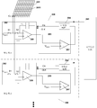
- FIG. 2 is a schematic structural diagram of a fingerprint identification circuit according to a first embodiment of the present application
- FIG. 3 is a schematic structural diagram of a comparator circuit of a fingerprint identification circuit according to a second embodiment of the present application.
- FIG. 4 is a schematic view showing a mounting structure of a cover plate and a capacitive fingerprint sensor of a mobile terminal according to a third embodiment of the present application.
- FIG. 1 is a schematic structural diagram of a typical capacitive fingerprint recognition circuit proposed by the applicant.
- the capacitive fingerprint recognition circuit mainly comprises a capacitive sensing array 101, a plurality of integrator circuits 102, a multiplexer (MUX) 103, a buffer 104, an analog to digital converter 105, and a digital algorithm circuit 106.
- the capacitive sensing array 101 includes a plurality of detecting plates 1011 distributed in an array of M rows and N columns to form the capacitive sensing array 101, M>1, N>1. Each of the detecting plates 1011 is connected to an integrator circuit 102 correspondingly.
- the same row integrator circuit 102 is connected to the analog to digital converter 105 through the multiplexer 103; and, in order to ensure signal quality, between the multiplexer 103 and the analog to digital converter 105 A buffer 104 can be connected.
- the analog to digital converter 105 is further coupled to the digital algorithm circuit 106 for analog to digital conversion of the fingerprint detection signal output by the integrator circuit 102 and output to the digital algorithm circuit 106 for digital algorithm processing.
- each integrator circuit 102 sequentially charges and discharges the fingerprint capacitance C P (ie, the capacitance formed by the corresponding detecting plate 1011 and the touch portion of the finger), and repeats the above. Operate until the predetermined number of charge and discharge cycles is completed. Thereafter, the output signal of the integrator circuit 102 is transmitted to the analog to digital converter 105 via the multiplexer 103 and the buffer 104. Analog to digital converter 105 converts the output signal of integrator circuit 102 into a digital signal and sends it to digital algorithm circuit 106.
- C P the capacitance formed by the corresponding detecting plate 1011 and the touch portion of the finger
- the digital algorithm circuit 106 After receiving the digital signal sent by the analog-to-digital converter 105, the digital algorithm circuit 106 can calculate the fingerprint capacitance C P between each detecting plate 1011 and the touched portion of the finger by processing the digital signal, thereby obtaining the user's Fingerprint information.
- the digital signal converted by the analog-to-digital converter 105 to the output signal of the integrator circuit 102 generally has a fixed number of bits, which may limit the subsequent digital algorithm circuit 106, that is, it is necessary to select and process the signal.
- the digital algorithm circuit of a fixed number of digital signals is difficult to be compatible with different types of digital algorithm circuits.
- due to the existence of the hardware circuit of the analog-to-digital converter 105 the cost, the difficulty of installing the design, and the power consumption are increased.
- the first embodiment of the present application provides a fingerprint identification circuit, which can acquire the fingerprint capacitance between each detecting plate and the touch portion of the finger without using an analog-to-digital converter, thereby acquiring the fingerprint of the finger. information.
- the fingerprint identification circuit can be applied to a capacitive fingerprint sensor, which includes a capacitive sensing array 201, a plurality of integration modules 208, and a digital algorithm circuit 205.
- the capacitive sensing array 201 includes a plurality of detecting plates 2011, and the plurality of detecting plates 2011 are distributed in an array of M rows and N columns to form the capacitive sensing array 201, wherein each of the detecting plates 2011 respectively corresponds to Connected to an integration module 208, and the outputs of the plurality of integration modules 208 are coupled to digital algorithm circuit 205.
- the plurality of detecting plates 2011 of the capacitive sensing array 201 are respectively coupled with the touch portion of the finger, and the fingerprint capacitors are respectively formed between the plurality of detecting plates 2011 and the fingers. C p .
- the fingerprint texture portion and a recessed portion of the protrusion detects its location different distances plate 2011, therefore, the fingerprint pattern and the capacitance C p between the valleys and ridges and detecting the detection plate 2011 fingerprint capacitance C p between the electrode plate 2011 are also different, so the value detected by the capacitance of the fingerprint capacitor C p finger can know which parts of the land, which is part of the valley lines, thereby acquiring the fingerprint information of the finger.
- the surface of the capacitive sensing array 201 of the fingerprint identification circuit is usually provided with a protective cover (such as a glass cover, a sapphire cover, a ceramic cover or a coating layer;
- the cover plate may also adopt a protective cover of the mobile terminal device. Therefore, the finger pressing the capacitive fingerprint sensor may actually refer to finger pressing the cover plate above the capacitive fingerprint sensor, wherein the dielectric layer acts as a cap plate fingerprint capacitance C p between the finger and the respective detection plate 2011 is formed of the coupling.
- the structure of the cover plate disposed above the capacitive fingerprint sensor can better protect the detecting plate 2011 of the capacitive sensing array 201 from damage.
- Each integrating module 208 is configured to charge the fingerprint capacitor C p corresponding to the connected detecting plate 2011, and transfer the charge of the fingerprint capacitor C p to the integrating capacitor for integration processing after each full charge (ie, the fingerprint discharge capacitance C p), and repeats the charging and charge transfer step, until the accumulated amount of charge transferred meets a preset condition.
- the integration module 208 can count the number of times of charging required when the total amount of accumulated transferred charges satisfies the preset condition, and send the charging number count value to the digital algorithm circuit 205.
- the digital algorithm circuit 205 can calculate the fingerprint capacitance C p between the detecting plate 2011 connected to the integrating module 208 and the touched portion of the finger by a digital algorithm according to the charging count value. Further, the digital algorithm circuit 205 can further calculate the fingerprint capacitance C p between all the detecting plates 2011 and the touch portion of the finger by the charging count value output by the plurality of integrating modules 208, thereby acquiring the finger Fingerprint information.
- each integration module 208 can include an integrator circuit 202, a comparator circuit 203, and a counter circuit 204.
- the integrator circuit 202 is connected to the corresponding detecting plate 2011 for charging the fingerprint capacitor C p corresponding to the connected detecting plate 2011, and transferring the charge of the fingerprint capacitor C p after being fully charged.
- the integral capacitor to its internal (ie, the feedback capacitor C f ).
- the comparator circuit 203 is configured to determine whether the total amount of accumulated current transferred charges satisfies a preset condition, and output the determination result to the counter circuit 204.
- the counter circuit 204 triggers the integrator circuit 202 to repeat the above charging and charge transfer process; if the total accumulated transferred charge amount satisfies the preset condition, the counter circuit 204 will send the number of times of the currently recorded integrator circuit 202 and send the number of times of charging to the subsequent digital algorithm circuit 205.
- the number of times of charging is the number of times of charging required when the total amount of accumulated transferred charges satisfies the preset condition.
- the counter circuit 204 can clear the count of the number of times of charging before performing fingerprint detection, and then control each time it receives the result of the judgment from the comparator circuit 203 (ie, the output signal of the comparator circuit).
- the charge count count value is internally incremented by 1, so that the current charge count value is the same as the charge count of the integrator circuit 202. Therefore, in this embodiment, the counter circuit 204 can use the current charging count value as the number of times of charging of the current integrator circuit 202, and output it to the digital algorithm circuit 205.
- the integrator circuit 202 may specifically include: a feedback capacitor C f , an operational amplifier 209, a first switch S1, a second switch S2, and a first input voltage V REF1 A connecting end and a second connecting end for connecting the detecting plate 2011.
- the first switch S1 is connected to the first connection end, the other end is connected to the second connection end and the second switch S2, and the other end of the second switch S2 is connected to the inverting input terminal of the operational amplifier 209;
- the non-inverting input is grounded;
- the output of the operational amplifier acts as the output of the integrator circuit 202 and is coupled to the comparator circuit 203;
- the feedback capacitor Cf is coupled between the inverting input and the output of the operational amplifier.
- the comparator circuit 203 mainly includes a comparator 207, the first input of the comparator circuit 203 is connected to the output of the integrator circuit 202 (ie, the output of the operational amplifier 209), and the second input of the comparator circuit 203 is used for inputting The second reference voltage V REF2 ; the output of the comparator circuit 203 is coupled to the counter circuit 204.
- the inverting input, the non-inverting input, and the output of comparator 207 can be coupled to a first input, a second input, and an output of comparator circuit 203, respectively.
- the charge of the fingerprint capacitor C p is transferred to the feedback capacitor C f located in the integrator circuit 202 ; wherein the amount of charge transferred to the feedback capacitor C f directly affects the operational amplifier The voltage at the output of 209.
- the comparator circuit 203 is based on the voltage of the voltage at the output of the current operational amplifier 209 to determine whether the total amount of accumulated current transferred charges satisfies a preset condition. Specifically, in the case where the finger presses the capacitive fingerprint sensor and forms a fingerprint capacitance C p with the detecting plate 2011, that is, the integrator circuit 202 can be based on the enable signal EN and the clock signal CLK provided by the counter circuit 204.
- the integrator circuit 202 can control the first switch S1 to open and control the second switch S2 to be closed.
- the transferred charge, C f represents the capacitance of the feedback capacitor.
- the integrator circuit 202 controls the closed and open states of the first switch S1 and the second switch S2 according to the enable signal EN and the clock signal CLK to repeat the above-mentioned fingerprint capacitance C f The process of charging and transferring the charged charge to the feedback capacitor Cf.
- the charge accumulation of the feedback capacitor C f is gradually increased, that is, the current accumulated transferred charge amount Q is more and more.
- the current accumulated transferred charge Q N*V REF1 *C p
- V REF1 represents the first reference voltage
- N represents the current number of times of charging (or the number of times of charge transfer)
- C p represents the capacitance value of the fingerprint capacitance.
- the non-inverting input end can also be used as the first
- An input terminal has an inverting input terminal as a second input terminal, which is not limited in this embodiment.
- the counter circuit 204 After receiving the high level signal from the comparator circuit 203, the counter circuit 204 sends an enable signal EN and a timing control signal (ie, a clock signal CLK) to the integrator circuit 202, and the trigger integrator circuit 202 controls the first switch S1.
- a timing control signal ie, a clock signal CLK
- the digital algorithm circuit 205 can calculate the fingerprint capacitance C p according to the charging count value.
- the voltage of the feedback capacitor C f Q.
- the difference between /C f and the second reference voltage V REF2 is very small.
- the digital algorithm circuit 205 can be This equation calculates the fingerprint capacitance C p .
- a digital arithmetic circuit 205 calculates out the method according to the above fingerprint capacitance C p between the touch pad and the detection portion of each finger, the finger so that the fingerprint information is known.
- the embodiment may also adopt a chopping method to calibrate the comparator 207 input mismatch to a relatively low level.
- the final number of times of charging (that is, the number of times of charging required when the total amount of accumulated transferred charges satisfies a preset condition) is controlled, thereby adjusting the digital signal output to the digital algorithm circuit 205.
- the range is advantageous for further improving the compatibility of the digital algorithm circuit 205.
- the fingerprint identification circuit provided by the embodiment does not need to use an analog-to-digital converter (ie, an ADC), and is also advantageous in saving cost, reducing design difficulty of the fingerprint identification circuit, and reducing power consumption.
- the second embodiment of the present application relates to a fingerprint identification circuit.
- This embodiment further improves the structure of the comparator circuit on the basis of the first embodiment.
- the main improvement is that in the embodiment, the comparator circuit 207 further includes a voltage dividing circuit.
- the comparator circuit includes a comparator and a voltage dividing circuit composed of the first voltage dividing unit and the second voltage dividing unit.
- the first voltage dividing unit includes a resistor R1
- the second voltage dividing unit includes a resistor R2.
- the first input of the comparator is connected to the output of the integrator circuit (ie, the output of the operational amplifier) through a resistor R1, and the second input of the comparator is used to input a second reference voltage V REF2 .
- One end of the resistor R2 is connected to the resistor R1 and the first input terminal of the comparator, and the other end is grounded.
- V out represents the output signal of the comparator.
- the comparator compares the magnitude relationship between V COMP and V REF2 to determine whether the total amount of accumulated charge currently meets the preset condition.
- the present embodiment can control the final charging frequency by adjusting the magnitude of the feedback capacitor C f , and can also control the final charging frequency by adjusting the ratio of the resistor R1 and the resistor R2, thereby adjusting the output.
- a third embodiment of the present application relates to a mobile terminal.
- the mobile terminal includes the fingerprint identification circuit described in the above embodiments.
- the mobile terminal can be a smart terminal such as a mobile phone or a tablet computer.
- the capacitive fingerprint sensor 210 can be placed under the cover plate 206.
- the cover plate 206 can be a protective cover of the mobile terminal (ie, the main glass cover), that is, the capacitive fingerprint sensor 210 is hidden under the protective cover.
- the protective cover can be By performing the thinning process at the corresponding position of the capacitive fingerprint sensor 210, the thickness of the cover plate of the area where the capacitive fingerprint sensor 210 is located is smaller than the thickness of other areas, so that the transmittance of the fingerprint detection signal can be improved.
- the cover plate 206 can be configured as a display screen of the mobile terminal (such as an OLED display screen), that is, the capacitive fingerprint sensor 210 is attached under the display screen to form a screen fingerprint recognition structure, and the screen is adopted.
- the fingerprint structure can meet the user's demand for high screen proportion of the front of the mobile terminal.
- the cover plate 206 may also refer to a glass cover plate, a ceramic cover plate, a sapphire cover plate or a coating layer attached to the surface of the capacitive fingerprint sensor 210.
- the capacitive fingerprint sensor 210 is a semiconductor sensor chip fabricated by a semiconductor fabrication process, and the capacitive sensing array 201 is placed on the uppermost layer of the capacitive fingerprint sensor 210.
- Finger by pressing the cover plate 206, so that the finger pressing portion 2011 is coupled to respective detection plates are formed fingerprint capacitor C p.
- the capacitive fingerprint sensor 210 is placed under the cover plate 206 to better protect the capacitive sensing array 201 on the surface of the capacitive fingerprint sensor 21.
- the range of the digital signal outputted to the digital algorithm circuit can be adjusted by adjusting the magnitude of the feedback capacitor C f or the ratio of the resistor R1 to the resistor R2, which is advantageous for improving the compatibility of the digital algorithm circuit.
- the fingerprint identification circuit provided by the embodiment does not need to use an analog-to-digital converter (ie, an ADC), and is also advantageous in saving cost, reducing design difficulty of the fingerprint identification circuit, and reducing power consumption.
- a fourth embodiment of the present application relates to a fingerprint sensor.
- the fingerprint sensor may include the fingerprint recognition circuit described in the first embodiment or the second embodiment.
- the fingerprint sensor can be applied to mobile terminals such as mobile phones and tablet computers.
Landscapes
- Engineering & Computer Science (AREA)
- Human Computer Interaction (AREA)
- Physics & Mathematics (AREA)
- General Physics & Mathematics (AREA)
- Multimedia (AREA)
- Theoretical Computer Science (AREA)
- Image Input (AREA)
- Measurement Of The Respiration, Hearing Ability, Form, And Blood Characteristics Of Living Organisms (AREA)
Abstract
L'invention concerne un circuit de reconnaissance d'empreinte digitale, un capteur d'empreinte digitale et un terminal mobile. Le circuit de reconnaissance d'empreinte digitale comprend un réseau de détection de capacité (201) et de multiples modules d'intégration (208), le réseau de détection de capacité (201) comprenant de multiples plaques polaires de détection (2011) agencées dans un réseau, et chaque plaque polaire de détection (2011) étant connectée de manière correspondante à un module d'intégration (208), respectivement ; la plaque polaire de détection (2011) est utilisée pour se coupler à une partie tactile d'un doigt et pour former un condensateur d'empreinte digitale (Cp) ; et le module d'intégration (208) est utilisé pour charger un condensateur d'empreinte digitale (Cp) correspondant à ce dernier, pour transférer la charge du condensateur d'empreinte digitale (Cp), et pour calculer une valeur de comptage du nombre d'instances de charge du condensateur d'empreinte digitale (Cp) lorsque la quantité totale de charges transférées de manière cumulative satisfait une condition prédéfinie, la valeur de comptage du nombre d'instances de charge étant utilisée pour indiquer une valeur de condensateur du condensateur d'empreinte digitale (Cp). Le circuit de reconnaissance d'empreinte digitale ne nécessite pas l'aide d'un convertisseur analogique-numérique, facilite l'amélioration de la compatibilité de différents types de circuits d'algorithmes numériques (205), et est propice à économiser des coûts, à réduire la difficulté de conception d'un circuit de reconnaissance d'empreinte digitale et à réduire la consommation d'énergie.
Priority Applications (2)
| Application Number | Priority Date | Filing Date | Title |
|---|---|---|---|
| PCT/CN2017/108875 WO2019084832A1 (fr) | 2017-11-01 | 2017-11-01 | Circuit de reconnaissance d'empreinte digitale, capteur d'empreinte digitale, et terminal mobile |
| CN201780001615.8A CN107980142B (zh) | 2017-11-01 | 2017-11-01 | 一种指纹识别电路、指纹传感器及移动终端 |
Applications Claiming Priority (1)
| Application Number | Priority Date | Filing Date | Title |
|---|---|---|---|
| PCT/CN2017/108875 WO2019084832A1 (fr) | 2017-11-01 | 2017-11-01 | Circuit de reconnaissance d'empreinte digitale, capteur d'empreinte digitale, et terminal mobile |
Publications (1)
| Publication Number | Publication Date |
|---|---|
| WO2019084832A1 true WO2019084832A1 (fr) | 2019-05-09 |
Family
ID=62006191
Family Applications (1)
| Application Number | Title | Priority Date | Filing Date |
|---|---|---|---|
| PCT/CN2017/108875 Ceased WO2019084832A1 (fr) | 2017-11-01 | 2017-11-01 | Circuit de reconnaissance d'empreinte digitale, capteur d'empreinte digitale, et terminal mobile |
Country Status (2)
| Country | Link |
|---|---|
| CN (1) | CN107980142B (fr) |
| WO (1) | WO2019084832A1 (fr) |
Cited By (4)
| Publication number | Priority date | Publication date | Assignee | Title |
|---|---|---|---|---|
| CN112073047A (zh) * | 2020-09-09 | 2020-12-11 | 上海东软载波微电子有限公司 | 电容式触摸按键系统及其控制方法 |
| CN114038023A (zh) * | 2021-11-29 | 2022-02-11 | 京东方科技集团股份有限公司 | 指纹识别装置及指纹识别方法 |
| CN114155564A (zh) * | 2021-11-18 | 2022-03-08 | 北京极豪科技有限公司 | 一种指纹信号采集电路、装置及电子设备 |
| TWI759959B (zh) * | 2020-04-30 | 2022-04-01 | 神盾股份有限公司 | 測量被動元件的測量電路 |
Families Citing this family (7)
| Publication number | Priority date | Publication date | Assignee | Title |
|---|---|---|---|---|
| CN109977911A (zh) * | 2019-04-08 | 2019-07-05 | 成都费恩格尔微电子技术有限公司 | 一种指纹识别电路、屏下指纹采集系统及采集方法 |
| TWI733427B (zh) * | 2019-08-16 | 2021-07-11 | 神盾股份有限公司 | 指紋感測裝置 |
| US11301708B2 (en) | 2019-10-01 | 2022-04-12 | Novatek Microelectronics Corp. | Image sensing circuit and method |
| KR20210101977A (ko) * | 2020-02-11 | 2021-08-19 | 삼성전자주식회사 | 지문 감지 장치 및 그 방법 |
| CN113785300B (zh) * | 2020-04-10 | 2024-07-26 | 京东方科技集团股份有限公司 | 指纹识别检测电路及其控制方法、指纹识别控制芯片 |
| CN112381007B (zh) * | 2020-11-17 | 2024-11-22 | 池州市谦跃信息技术有限公司 | 指纹信息获取方法、装置、存储介质及终端 |
| CN119804999B (zh) * | 2025-03-12 | 2025-06-17 | 成都维客昕微电子有限公司 | 一种电容检测电路、方法及设备 |
Citations (4)
| Publication number | Priority date | Publication date | Assignee | Title |
|---|---|---|---|---|
| US20050163350A1 (en) * | 2002-03-09 | 2005-07-28 | Melfas Co. Ltd | Fingerprint sensing apparatus and method using time-variable propertz of fingerpring signal |
| CN102954753A (zh) * | 2012-10-22 | 2013-03-06 | 成都微阵列电子有限责任公司 | 电容式距离传感器 |
| CN103714330A (zh) * | 2014-01-06 | 2014-04-09 | 李扬渊 | 电容指纹传感器 |
| CN105512650A (zh) * | 2016-01-26 | 2016-04-20 | 湖南融创微电子有限公司 | 一种电容式指纹检测电路、传感器及设备 |
Family Cites Families (4)
| Publication number | Priority date | Publication date | Assignee | Title |
|---|---|---|---|---|
| CN105488451B (zh) * | 2014-09-26 | 2019-07-12 | 上海思立微电子科技有限公司 | 一种指纹识别传感器 |
| US10068123B2 (en) * | 2015-12-18 | 2018-09-04 | Electronics And Telecommunications Research Institute | Fingerprint sensor and electronic device having the same |
| EP3324331B1 (fr) * | 2016-09-27 | 2020-11-25 | Shenzhen Goodix Technology Co., Ltd. | Circuit de détection capacitif |
| EP3321848B1 (fr) * | 2016-09-27 | 2019-12-25 | Shenzhen Goodix Technology Co., Ltd. | Circuit de détection capacitif |
-
2017
- 2017-11-01 CN CN201780001615.8A patent/CN107980142B/zh active Active
- 2017-11-01 WO PCT/CN2017/108875 patent/WO2019084832A1/fr not_active Ceased
Patent Citations (4)
| Publication number | Priority date | Publication date | Assignee | Title |
|---|---|---|---|---|
| US20050163350A1 (en) * | 2002-03-09 | 2005-07-28 | Melfas Co. Ltd | Fingerprint sensing apparatus and method using time-variable propertz of fingerpring signal |
| CN102954753A (zh) * | 2012-10-22 | 2013-03-06 | 成都微阵列电子有限责任公司 | 电容式距离传感器 |
| CN103714330A (zh) * | 2014-01-06 | 2014-04-09 | 李扬渊 | 电容指纹传感器 |
| CN105512650A (zh) * | 2016-01-26 | 2016-04-20 | 湖南融创微电子有限公司 | 一种电容式指纹检测电路、传感器及设备 |
Cited By (5)
| Publication number | Priority date | Publication date | Assignee | Title |
|---|---|---|---|---|
| TWI759959B (zh) * | 2020-04-30 | 2022-04-01 | 神盾股份有限公司 | 測量被動元件的測量電路 |
| US11460495B2 (en) | 2020-04-30 | 2022-10-04 | Egis Technology Inc. | Measurement circuit and method for measuring characteristic of passive component by means of comparison signals |
| CN112073047A (zh) * | 2020-09-09 | 2020-12-11 | 上海东软载波微电子有限公司 | 电容式触摸按键系统及其控制方法 |
| CN114155564A (zh) * | 2021-11-18 | 2022-03-08 | 北京极豪科技有限公司 | 一种指纹信号采集电路、装置及电子设备 |
| CN114038023A (zh) * | 2021-11-29 | 2022-02-11 | 京东方科技集团股份有限公司 | 指纹识别装置及指纹识别方法 |
Also Published As
| Publication number | Publication date |
|---|---|
| CN107980142A (zh) | 2018-05-01 |
| CN107980142B (zh) | 2021-07-20 |
Similar Documents
| Publication | Publication Date | Title |
|---|---|---|
| CN107980142B (zh) | 一种指纹识别电路、指纹传感器及移动终端 | |
| JP6750059B2 (ja) | 改良された感知素子を備えた容量指紋センサ | |
| TWI391678B (zh) | 電容值測量電路與其方法 | |
| CN211860069U (zh) | 电容感测装置 | |
| JP6810739B2 (ja) | コモンモード抑圧の指紋感知装置 | |
| TWI531979B (zh) | 電容指紋感測器 | |
| US11954283B2 (en) | High resolution touch sensor apparatus and method | |
| US20160063301A1 (en) | Capacitive fingerprint sensor and fingerprint sensing method thereof | |
| CN108121469B (zh) | 触控装置及其唤醒方法 | |
| CN104748770B (zh) | 用于指纹识别的电容检测装置和具有其的指纹识别装置 | |
| US10408862B2 (en) | Multiple channel capacitive voltage divider scanning method and apparatus | |
| WO2019144303A1 (fr) | Circuit de détection de capacité, appareil tactile et équipement terminal | |
| WO2016130070A1 (fr) | Dispositif de détection d'empreinte digitale capacitive comprenant un affichage de courant à partir d'éléments de détection | |
| KR101810543B1 (ko) | 동기신호 입력부를 갖는 지문센서 | |
| TWI613599B (zh) | 具有調適性電力控制之指紋感測系統及其操作方法 | |
| CN108701226A (zh) | 指纹传感器和终端设备 | |
| CN110210349B (zh) | 指纹传感器和移动终端 | |
| KR102248984B1 (ko) | 고감도 터치 센서 | |
| CN110597411A (zh) | 压力检测电路、电子设备和压力检测电路的控制方法 | |
| CN106201140B (zh) | 触控装置与其感测方法 | |
| CN113541668B (zh) | 触摸感测方法、电路以及电子设备 | |
| EP4205020A1 (fr) | Capteur biométrique en contact avec la peau et procédé de fonctionnement d'un capteur biométrique en contact avec la peau | |
| KR102052941B1 (ko) | 터치 압력 정보를 활용하는 지문 검출 장치 및 지문 검출 방법 | |
| CN107633230B (zh) | 一种高效手指电容检测电路 | |
| CN215068273U (zh) | 指纹识别模组、芯片及电子设备 |
Legal Events
| Date | Code | Title | Description |
|---|---|---|---|
| 121 | Ep: the epo has been informed by wipo that ep was designated in this application |
Ref document number: 17930549 Country of ref document: EP Kind code of ref document: A1 |
|
| NENP | Non-entry into the national phase |
Ref country code: DE |
|
| 122 | Ep: pct application non-entry in european phase |
Ref document number: 17930549 Country of ref document: EP Kind code of ref document: A1 |