WO2019087655A1 - Circuit de filtrage, onduleur et appareil d'alimentation électrique - Google Patents
Circuit de filtrage, onduleur et appareil d'alimentation électrique Download PDFInfo
- Publication number
- WO2019087655A1 WO2019087655A1 PCT/JP2018/036912 JP2018036912W WO2019087655A1 WO 2019087655 A1 WO2019087655 A1 WO 2019087655A1 JP 2018036912 W JP2018036912 W JP 2018036912W WO 2019087655 A1 WO2019087655 A1 WO 2019087655A1
- Authority
- WO
- WIPO (PCT)
- Prior art keywords
- positive
- negative
- output terminal
- side output
- capacitor
- Prior art date
- Legal status (The legal status is an assumption and is not a legal conclusion. Google has not performed a legal analysis and makes no representation as to the accuracy of the status listed.)
- Ceased
Links
Images



Classifications
-
- H—ELECTRICITY
- H02—GENERATION; CONVERSION OR DISTRIBUTION OF ELECTRIC POWER
- H02M—APPARATUS FOR CONVERSION BETWEEN AC AND AC, BETWEEN AC AND DC, OR BETWEEN DC AND DC, AND FOR USE WITH MAINS OR SIMILAR POWER SUPPLY SYSTEMS; CONVERSION OF DC OR AC INPUT POWER INTO SURGE OUTPUT POWER; CONTROL OR REGULATION THEREOF
- H02M7/00—Conversion of AC power input into DC power output; Conversion of DC power input into AC power output
- H02M7/003—Constructional details, e.g. physical layout, assembly, wiring or busbar connections
-
- H—ELECTRICITY
- H02—GENERATION; CONVERSION OR DISTRIBUTION OF ELECTRIC POWER
- H02M—APPARATUS FOR CONVERSION BETWEEN AC AND AC, BETWEEN AC AND DC, OR BETWEEN DC AND DC, AND FOR USE WITH MAINS OR SIMILAR POWER SUPPLY SYSTEMS; CONVERSION OF DC OR AC INPUT POWER INTO SURGE OUTPUT POWER; CONTROL OR REGULATION THEREOF
- H02M7/00—Conversion of AC power input into DC power output; Conversion of DC power input into AC power output
- H02M7/42—Conversion of DC power input into AC power output without possibility of reversal
- H02M7/44—Conversion of DC power input into AC power output without possibility of reversal by static converters
- H02M7/48—Conversion of DC power input into AC power output without possibility of reversal by static converters using discharge tubes with control electrode or semiconductor devices with control electrode
- H02M7/53—Conversion of DC power input into AC power output without possibility of reversal by static converters using discharge tubes with control electrode or semiconductor devices with control electrode using devices of a triode or transistor type requiring continuous application of a control signal
- H02M7/537—Conversion of DC power input into AC power output without possibility of reversal by static converters using discharge tubes with control electrode or semiconductor devices with control electrode using devices of a triode or transistor type requiring continuous application of a control signal using semiconductor devices only, e.g. single switched pulse inverters
- H02M7/5387—Conversion of DC power input into AC power output without possibility of reversal by static converters using discharge tubes with control electrode or semiconductor devices with control electrode using devices of a triode or transistor type requiring continuous application of a control signal using semiconductor devices only, e.g. single switched pulse inverters in a bridge configuration
-
- H—ELECTRICITY
- H02—GENERATION; CONVERSION OR DISTRIBUTION OF ELECTRIC POWER
- H02M—APPARATUS FOR CONVERSION BETWEEN AC AND AC, BETWEEN AC AND DC, OR BETWEEN DC AND DC, AND FOR USE WITH MAINS OR SIMILAR POWER SUPPLY SYSTEMS; CONVERSION OF DC OR AC INPUT POWER INTO SURGE OUTPUT POWER; CONTROL OR REGULATION THEREOF
- H02M7/00—Conversion of AC power input into DC power output; Conversion of DC power input into AC power output
- H02M7/66—Conversion of AC power input into DC power output; Conversion of DC power input into AC power output with possibility of reversal
- H02M7/68—Conversion of AC power input into DC power output; Conversion of DC power input into AC power output with possibility of reversal by static converters
- H02M7/72—Conversion of AC power input into DC power output; Conversion of DC power input into AC power output with possibility of reversal by static converters using discharge tubes with control electrode or semiconductor devices with control electrode
- H02M7/79—Conversion of AC power input into DC power output; Conversion of DC power input into AC power output with possibility of reversal by static converters using discharge tubes with control electrode or semiconductor devices with control electrode using devices of a triode or transistor type requiring continuous application of a control signal
- H02M7/797—Conversion of AC power input into DC power output; Conversion of DC power input into AC power output with possibility of reversal by static converters using discharge tubes with control electrode or semiconductor devices with control electrode using devices of a triode or transistor type requiring continuous application of a control signal using semiconductor devices only
-
- H—ELECTRICITY
- H02—GENERATION; CONVERSION OR DISTRIBUTION OF ELECTRIC POWER
- H02M—APPARATUS FOR CONVERSION BETWEEN AC AND AC, BETWEEN AC AND DC, OR BETWEEN DC AND DC, AND FOR USE WITH MAINS OR SIMILAR POWER SUPPLY SYSTEMS; CONVERSION OF DC OR AC INPUT POWER INTO SURGE OUTPUT POWER; CONTROL OR REGULATION THEREOF
- H02M1/00—Details of apparatus for conversion
- H02M1/14—Arrangements for reducing ripples from DC input or output
-
- H—ELECTRICITY
- H02—GENERATION; CONVERSION OR DISTRIBUTION OF ELECTRIC POWER
- H02M—APPARATUS FOR CONVERSION BETWEEN AC AND AC, BETWEEN AC AND DC, OR BETWEEN DC AND DC, AND FOR USE WITH MAINS OR SIMILAR POWER SUPPLY SYSTEMS; CONVERSION OF DC OR AC INPUT POWER INTO SURGE OUTPUT POWER; CONTROL OR REGULATION THEREOF
- H02M5/00—Conversion of AC power input into AC power output, e.g. for change of voltage, for change of frequency, for change of number of phases
- H02M5/02—Conversion of AC power input into AC power output, e.g. for change of voltage, for change of frequency, for change of number of phases without intermediate conversion into DC
- H02M5/04—Conversion of AC power input into AC power output, e.g. for change of voltage, for change of frequency, for change of number of phases without intermediate conversion into DC by static converters
- H02M5/22—Conversion of AC power input into AC power output, e.g. for change of voltage, for change of frequency, for change of number of phases without intermediate conversion into DC by static converters using discharge tubes with control electrode or semiconductor devices with control electrode
- H02M5/275—Conversion of AC power input into AC power output, e.g. for change of voltage, for change of frequency, for change of number of phases without intermediate conversion into DC by static converters using discharge tubes with control electrode or semiconductor devices with control electrode using devices of a triode or transistor type requiring continuous application of a control signal
- H02M5/293—Conversion of AC power input into AC power output, e.g. for change of voltage, for change of frequency, for change of number of phases without intermediate conversion into DC by static converters using discharge tubes with control electrode or semiconductor devices with control electrode using devices of a triode or transistor type requiring continuous application of a control signal using semiconductor devices only
-
- H—ELECTRICITY
- H02—GENERATION; CONVERSION OR DISTRIBUTION OF ELECTRIC POWER
- H02M—APPARATUS FOR CONVERSION BETWEEN AC AND AC, BETWEEN AC AND DC, OR BETWEEN DC AND DC, AND FOR USE WITH MAINS OR SIMILAR POWER SUPPLY SYSTEMS; CONVERSION OF DC OR AC INPUT POWER INTO SURGE OUTPUT POWER; CONTROL OR REGULATION THEREOF
- H02M5/00—Conversion of AC power input into AC power output, e.g. for change of voltage, for change of frequency, for change of number of phases
- H02M5/40—Conversion of AC power input into AC power output, e.g. for change of voltage, for change of frequency, for change of number of phases with intermediate conversion into DC
- H02M5/42—Conversion of AC power input into AC power output, e.g. for change of voltage, for change of frequency, for change of number of phases with intermediate conversion into DC by static converters
- H02M5/44—Conversion of AC power input into AC power output, e.g. for change of voltage, for change of frequency, for change of number of phases with intermediate conversion into DC by static converters using discharge tubes or semiconductor devices to convert the intermediate DC into AC
- H02M5/443—Conversion of AC power input into AC power output, e.g. for change of voltage, for change of frequency, for change of number of phases with intermediate conversion into DC by static converters using discharge tubes or semiconductor devices to convert the intermediate DC into AC using devices of a thyratron or thyristor type requiring extinguishing means
- H02M5/45—Conversion of AC power input into AC power output, e.g. for change of voltage, for change of frequency, for change of number of phases with intermediate conversion into DC by static converters using discharge tubes or semiconductor devices to convert the intermediate DC into AC using devices of a thyratron or thyristor type requiring extinguishing means using semiconductor devices only
- H02M5/4505—Conversion of AC power input into AC power output, e.g. for change of voltage, for change of frequency, for change of number of phases with intermediate conversion into DC by static converters using discharge tubes or semiconductor devices to convert the intermediate DC into AC using devices of a thyratron or thyristor type requiring extinguishing means using semiconductor devices only having a rectifier with controlled elements
Definitions
- the present invention relates to a smoothing circuit, an inverter, and a power supply apparatus.
- AC power supplied to a heating coil used for induction heating is generally generated through a process of converting AC power of a commercial power supply into DC power through a converter and inversely converting the converted DC power into AC power of a desired frequency through an inverter.
- the inverter includes a plurality of power semiconductor devices, and the inverse conversion from DC power to AC power is performed by switching operations of the plurality of power semiconductor devices.
- a first related art power conversion apparatus includes a first smoothing capacitor and a second smoothing capacitor having a smaller capacitance and high-frequency impedance than the first smoothing capacitor and disposed more adjacent to a semiconductor switching element than the first smoothing capacitor (see, e.g., to JP2004-254355A).
- a second related art power supply apparatus includes a plurality of capacitors arranged adjacent to a power semiconductor device, and the plurality of capacitors are connected in parallel to each other (see, e.g., JP2017-004593A).
- a high-speed switching operation of the power semiconductor device rapidly changes a current flowing through the power semiconductor device, and the current change di/dt generates a surge voltage (L ⁇ di/dt) across the power semiconductor device through inductance L such as inductance of an electrical path between the power semiconductor device and a capacitor serving as a voltage source or internal inductance of the capacitor.
- An excessive surge voltage may destroy the power semiconductor device, and thus needs to be prevented. Since the current change di/dt is mainly decided by the characteristics of the power semiconductor device, the surge voltage can be prevented by reducing the inductance L.
- the capacitor may be disposed adjacent to the power semiconductor device. Accordingly, the inductance of the electrical path between the power semiconductor device and the capacitor can be reduced.
- the plurality of capacitors may be arranged adjacent to the power semiconductor device, and connected in parallel to each other. Accordingly, equivalent inductance corresponding to combined internal inductance of the plurality of capacitors can be reduced, and smaller capacitors can be disposed close to the power semiconductor device.
- Illustrative aspects of the present invention provide a smoothing circuit capable of suppressing a surge voltage from occurring in an inverter, and uniformly distributing current to a plurality of capacitors provided in a smoothing circuit of a voltage-type power supply, thereby preventing damage due to heat generated in the respective capacitors.
- a smoothing circuit includes a plate-shaped circuit body having a positive-side output terminal and a negative-side output terminal, and a plurality of capacitors mounted on the circuit body and connected to each other in parallel between the positive-side output terminal and the negative-side output terminal, each capacitor having a positive terminal and a negative terminal.
- the circuit body includes, for each capacitor, a positive electrical path connecting the positive terminal of the capacitor and the positive-side output terminal to each other and a negative electrical path connecting the negative terminal of the capacitor and the negative-side output terminal to each other.
- a difference between a maximum positive-negative electrical path length and a minimum positive-negative electrical path length among the positive-negative electrical path lengths is equal to or smaller than 30% of the minimum positive-negative electrical path length.
- a smoothing circuit includes a plate-shaped circuit body having a positive-side output terminal and a negative-side output terminal, and a plurality of capacitors mounted on the circuit body and connected to each other in parallel between the positive-side output terminal and the negative-side output terminal, each capacitor having a positive terminal and a negative terminal.
- the circuit body includes a positive solid pattern providing, for each capacitor, a positive electrical path connecting the positive terminal of the capacitor and the positive-side output terminal to each other, a negative solid pattern providing, for each capacitor, a negative electrical path connecting the negative terminal of the capacitor and the negative-side output terminal to each other, and an insulating layer interposed between the positive solid pattern and the negative solid pattern.
- a difference between a maximum distance and a minimum distance among distances to the respective capacitors is equal to or smaller than 30% of the minimum distance.
- an inverter includes the smoothing circuit described above, and an inverter circuit connected to the positive-side output terminal and the negative-side output terminal of the smoothing circuit, and configured to convert DC power supplied from the smoothing circuit into AC power.
- a power supply apparatus includes the inverter described above, and a converter configured to convert AC power supplied from an AC power supply into DC power to supply the DC power to the smoothing circuit of the inverter.
- Illustrative aspects of the present invention can provide a smoothing circuit capable of suppressing a surge voltage from occurring in an inverter, and can also provide an inverter and a power supply apparatus having improved protection for power semiconductor devices.
- Fig. 1 is a block diagram illustrating an example of a power supply apparatus according to an embodiment of the present invention.
- Fig. 2 is a schematic diagram illustrating a configuration example of a smoothing circuit of Fig. 1.
- Fig. 3 is a cross-sectional view of the smoothing circuit, taken along the line III-III of Fig. 2.
- Fig. 4 is a schematic diagram illustrating another configuration example of the smoothing circuit of Fig. 1.
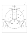
- Fig. 5 is a schematic diagram illustrating still another configuration example of the smoothing circuit of Fig. 1.
- Fig. 1 illustrates an example of a power supply apparatus according to an embodiment of the present invention.
- the power supply apparatus 1 includes a converter 3 configured to convert AC power supplied from an AC power supply 2 into DC power and an inverter 4 configured to convert the DC power output from the converter 3 into AC power.
- the converter 3 may perform rectification using a diode bridge, for example, or perform rectification to vary an output voltage, using a semiconductor device such as a thyristor capable of controlling conduction based on an external signal.
- the inverter 4 has four power semiconductor devices Q1 to Q4 each configured to perform a switching operation.
- a first leg QL1 includes the power semiconductor device Q1 and the power semiconductor device Q2 connected to each other in series.
- the power semiconductor device Q1 is provided as an upper arm and the power semiconductor device Q2 is provided as a lower arm.
- a second leg QL2 includes the power semiconductor device Q3 and the power semiconductor device Q4 connected to each other in series.
- the power semiconductor device Q3 is provided as an upper arm and the power semiconductor device Q4 is provided as a lower arm.
- the first leg QL1 and the second leg QL2 together form an inverter circuit Inv.
- the upper arm (the power semiconductor device Q1) of the first leg QL1 and the lower arm (the power semiconductor device Q4) of the second leg QL2 are turned on in synchronization with each other, and the lower arm (the power semiconductor device Q2) of the first leg QL1 and the upper arm (the power semiconductor Q3) of the second leg QL2 are turned on in synchronization with each other. Furthermore, the upper arm of the first leg QL1 and the lower arm of the second leg QL2 and the lower arm of the first leg QL1 and the upper arm of the second leg QL2 are alternately turned on in cycles. Accordingly, AC power is generated from DC power, and outputted from a serial contact point between the upper arm and the lower arm of each of the first leg QL1 and the second leg QL2.
- a load 5 including a heating coil is connected to an AC output of the inverter 4, and the AC power generated by the inverter 4 is supplied to the heating coil. Furthermore, a heating target is induction-heated by the heating coil.
- the heating target and the heating purpose are not specifically limited, and a heat treatment (e.g., quenching) for a steel material can be exemplified.
- the power semiconductor device may include various types of power semiconductor devices capable of performing a switching operation, such as an insulated gate bipolar transistor (IGBT) and metal-oxide-semiconductor field-effect transistor (MOSFET), and silicon (Si) or silicon carbide (SiC) may be used as the semiconductor material.
- IGBT insulated gate bipolar transistor
- MOSFET metal-oxide-semiconductor field-effect transistor
- Si silicon
- SiC silicon carbide
- the inverter circuit Inv may constitute first to third legs using six power semiconductor devices, and generate three-phase AC power.
- the inverter 4 may include a plurality of inverter circuits Inv. When the inverter 4 includes the plurality of inverter circuits Inv, AC powers generated by the respective inverter circuits Inv are combined, and the combined AC power is supplied to the load 5 from the inverter 4.
- the inverter 4 further includes a smoothing circuit 7.
- the smoothing circuit 7 smoothes DC power containing a ripple, which is output from the converter 3, and supplies the smoothed DC power to the inverter circuit Inv.
- one smoothing circuit 7 is provided for one inverter circuit Inv.
- one smoothing circuit 7 may be provided for the plurality of inverter circuits Inv, or a plurality of smoothing circuits 7 may be used so that one smoothing circuit 7 is provided for one inverter circuit Inv.
- one smoothing circuit 7 is provided for the inverter circuit Inv including the first and second legs QL1, QL2.
- two smoothing circuits 7 may be used so that one smoothing circuit 7 is provided for each of the first and second legs QL1, QL2.
- three smoothing circuits 7 can be used and provided for the first to third legs, respectively.
- the smoothing circuit 7 includes a plurality of capacitors connected in parallel to a DC output of the converter 3 and a DC input of the inverter circuit Inv.
- the smoothing circuit 7 includes three capacitors C1, C2, C3.
- the capacitors C1, C2, C3 are mounted in a plate-shaped circuit body, and the circuit body includes a positive-side output terminal P connected to a positive side of the DC input of the inverter circuit Inv and a negative-side output terminal N connected to a negative side of the DC input of the inverter circuit Inv.
- the positive-side output terminal P and the negative-side output terminal N also serve as input terminals connected to the DC output of the converter 3, but the input terminals may be separately provided.
- the capacitor C1 has a capacitance component C C1 , a resistance component R C1 and an inductance component L C1 therein. Furthermore, a resistance component RP1 and an inductance component L P1 are present in a positive electrical path between a positive terminal P C1 of the capacitor C1 and the positive-side output terminal P of the circuit body, and a resistance component R N1 and an inductance component L N1 are also present in a negative electrical path between a negative terminal N C1 of the capacitor C1 and the negative-side output terminal N of the circuit body.
- the capacitor C2 has a capacitance component C C2 , a resistance component R C2 and an inductance component L C2 therein, a resistance component R P2 and an inductance component L P2 are present in a positive electrical path between a positive terminal P C2 of the capacitor C2 and the positive-side output terminal P of the circuit body, and a resistance component R N2 and an inductance component L N2 are present in a negative electrical path between a negative terminal N C2 of the capacitor C2 and the negative-side output terminal N of the circuit body.
- the capacitor C3 also has a capacitance component C C3 , a resistance component R C3 and an inductance component L C3 therein, a resistance component R P3 and an inductance component L P3 are present in a positive electrical path between a positive terminal P C3 of the capacitor C3 and the positive-side output terminal P of the circuit body, and a resistance component R N3 and an inductance component L N3 are present in a negative electrical path between a negative terminal N C3 of the capacitor C3 and the negative-side output terminal N of the circuit body.
- the resistance component Ri typically has an extremely small value in the order of m ⁇ , and a dominant element deciding the high-frequency impedance Zi is considered as the inductance component Li. Therefore, when the inductance components Li are uniformized, it is possible to reduce a variation of the high-frequency impedances Zi, thereby preventing a variation in the currents flowing through the capacitors C1, C2, C3.
- the configuration of the smoothing circuit 7 for uniformizing the inductances L PNi of the positive and negative electrical paths in the respective capacitors will be described.
- Figs. 2 and 3 illustrate a configuration example of the smoothing circuit 7.
- the circuit body 10 illustrated in Figs. 2 and 3 is a so-called laminated bus bar in which metal plates 12, 13 such as copper plates are provided as layers on the front and back surfaces of an insulating sheet 11 in a laminated manner.
- the circuit body 10 is not limited to the laminated bus bar, and may include a bus bar, a power board substrate and the like.
- the metal plate 12 provided as a layer on the front surface of the insulating sheet 11 includes a positive-side output terminal P and three strip-shaped conductors P-P1, P-P2, P-P3 extending in a branched manner from the positive-side output terminal P.
- the three conductors P-P1, P-P2, P-P3 have terminals P1, P2, P3 provided at respective ends thereof (ends at the opposite side of the positive-side output terminal P) and connected to the positive terminals PC1, PC2, PC3 of the capacitors C1, C2, C3, respectively.
- the conductors P-P1, P-P2, P-P3 form the positive electrical paths for the capacitors C1, C2, C3.
- the metal plate 13 provided as a layer on the back surface of the insulating sheet 11 includes a negative-side output terminal N and three strip-shaped conductors N-N1, N-N2, N-N3 extending in a branched manner from the negative-side output terminal N.
- the three conductors N-N1, N-N2, N-N3 have terminals N1, N2, N3 provided at respective ends thereof (ends at the opposite side of the negative-side output terminal N) and connected to the negative terminals NC1 to NC3 of the capacitors C1, C2, C3, respectively.
- the conductors N-N1, N-N2, N-N3 form the negative electrical paths for the capacitors C1, C2, C3.
- the strip-shaped conductors P-P1, P-P2, P-P3, N-N1, N-N2, N-N3 have substantially the same width.
- the positive-side output terminal P has a hole passing through the circuit body 10, such that the positive-side terminal of the DC input of the inverter circuit Inv (see Fig. 1) or the bus bar connected to the positive-side terminal is screwed to the positive-side output terminal P, and the terminals P1, P2, P3 of the conductors P-P1, P-P2, P-P3 also have holes passing through the circuit body 10, such that the positive terminals PC1, PC2, PC3 of the capacitors C1, C2, C3 are screwed to the respective terminals P1, P2, P3.
- the positive-side output terminal P and the terminals P1, P2, P3 are not limited to screw terminals.
- the negative-side output terminal N and the terminals N1, N2, N3 of the conductors N-N1, N-N2, N-N3 are not limited to screw terminals.
- the metal plates 12, 13 are coated with an insulating layer while the terminals P, P1, P2, P3, N and N1, N2, N3 are exposed.
- the length ln P1 of the strip-shaped conductor P-P1 is the length of the positive electrical path for the capacitor C1
- the length ln N1 of the strip-shaped conductor N-N1 is the length of the negative electrical path for the capacitor C1
- the length ln P2 of the strip-shaped conductor P-P2 is the length of the positive electrical path for the capacitor C2
- the length ln N2 of the strip-shaped conductor N-N2 is the length of the negative electrical path for the capacitor C2
- the length ln P3 of the strip-shaped conductor P-P3 is the length of the positive electrical path for the capacitor C3
- the length ln N3 of the strip-shaped conductor N-N3 is the length of the negative electrical path for the capacitor C3
- the positive-negative electrical path lengths ln PN1 , ln PN2 , ln PN3 for the respective capacitors C1, C2, C3 correspond to the inductances L PN1 to L PN3 of the positive-negative electrical paths for the capacitors C1, C2, C3. Therefore, when the positive-negative electrical path lengths ln PN1 , ln PN2 , ln PN3 are uniformized, the inductances L PN1 to L PN3 of the positive-negative electrical paths for the capacitors C1, C2, C3 are uniformized.
- the difference ⁇ ln is equal to or greater than 50% of ln min in related art smoothing circuits including a plurality of capacitors
- the difference ⁇ ln may be designed to be, for example, equal to or smaller than 30% of ln min ( ⁇ ln ⁇ 0.3 ⁇ ln min ).
- Fig. 4 illustrates another example of a configuration of the smoothing circuit 7.
- a circuit body 20 is configured as a laminated bus bar like the circuit body 10 described above.
- a metal plate provided as a layer on the front surface of the insulating sheet and forming the positive electrical paths for the capacitors C1, C2, C3 is configured as a solid pattern covering the entire front surface of the insulating sheet
- a metal plate provided as a layer on the back surface of the insulating sheet and forming the negative electrical paths for the capacitors C1, C2, C3 is configured as a solid pattern covering the entire back surface of the insulating sheet.
- the metal plate layer on the front surface of the insulating sheet includes a positive-side output terminal P and terminals P1, P2, P3 to which the positive terminals PC1, PC2, PC3 of the capacitors C1, C2, C3 are connected.
- the positive-side output terminal P is provided approximately at the center of the circuit body 20, and the terminals P1, P2, P3 are arranged around the positive-side output terminal P. Since current flows along the shortest path of a homogeneous conductor, a straight line P-P1 connecting the positive-side output terminal P and the terminal P1 becomes the positive electrical path for the capacitor C1.
- a straight line P-P2 connecting the positive-side output terminal P and the terminal P2 becomes the positive electrical path for the capacitor C2
- a straight line P-P3 connecting the positive-side output terminal P and the terminal P3 becomes the positive electrical path for the capacitor C3.
- the metal plate layer on the back surface of the insulating sheet includes a negative-side output terminal N and terminals N1, N2, N3 to which the negative terminals N C1 to N C3 of the capacitors C1, C2, C3 are connected.
- the negative-side output terminal N is provided approximately at the center of the circuit body 20 and provided adjacent to the positive-side output terminal.
- the terminals N1, N2, N3 are arranged around the negative-side output terminal N.
- the terminal N1 is provided adjacent to the terminal P1
- the terminal N2 is provided adjacent to the terminal P2
- the terminal N3 is provided adjacent to the terminal P3.
- a straight line N-N1 connecting the negative-side output terminal N and the terminal N1 becomes the negative electrical path for the capacitor C1
- a straight line N-N2 connecting the negative-side output terminal N and the terminal N2 becomes the negative electrical path for the capacitor C2
- a straight line N-N3 connecting the negative-side output terminal N and the terminal N3 becomes the negative electrical path for the capacitor C3.
- the length lnP1 of the straight line P-P1 is the length of the positive electrical path for the capacitor C1
- the length ln N1 of the straight line N-N1 is the length of the negative electrical path for the capacitor C1
- the length ln P2 of the straight line P-P2 is the length of the positive electrical path for the capacitor C2
- the length ln N2 of the straight line N-N2 is the length of the negative electrical path for the capacitor C2
- the length lnP3 of the straight line P-P3 is the length of the positive electrical path for the capacitor C3
- the length ln N3 of the straight line N-N3 is the length of the negative electrical path length for the capacitor C3
- the positive-negative electrical path lengths ln PN1 , ln PN2 , ln PN3 for the respective capacitors C1, C2, C3 correspond to the inductances L PN1 to L PN3 of the positive-negative electrical paths for the capacitors C1, C2, C3, as in the above-described circuit body 10.
- the positive-negative electrical path lengths ln PN1 , ln PN2 , ln PN3 for the capacitors C1, C2, C3 can be replaced with distances from the positive-side output terminal P and the negative-side output terminal N to the capacitors C1, C2, C3.
- the middle point M P1-N1 between the terminal P1 (the positive terminal P C1 ) and the terminal N1 (the negative terminal N C1 ) is defined as the position of the capacitor C1.
- the middle point M P2-N2 between the terminal P2 (the positive terminal P C2 ) and the terminal N2 (the negative terminal N C2 ) is defined as the position of the capacitor C2
- the middle point M P3-N3 between the terminal P3 (the positive terminal P C3 ) and the terminal N3 (the negative terminal N C3 ) is defined as the position of the capacitor C3.
- a distance to the middle point M P1-N1 is defined as a distance d1 to the capacitor C1
- a distance to the middle point M P2-N2 is defined as a distance d2 of the capacitor C2
- a distance to the middle point M P3-N3 is defined as a distance d3 of the capacitor C3.
- the terminals P1, P2, P3 and the terminals N1, N2, N3 are arranged on a circle O1 centered on the middle point M P-N between the positive-side output terminal P and the negative-side output terminal N.
- the middle points M P1-N1 , M P2-N2 , M P3-N3 of the capacitors C1, C2, C3, defining the distances d1 to d3, are also arranged on another circle O centered on the middle point M P-N . Accordingly, the distances d1 to d3 of the capacitors C1, C2, C3 become equal to each other, and ⁇ d becomes nearly zero.
- the inductance components L P1 , L P2 , L P3 of the positive electrical paths and the inductance components L N1 , L N2 , L N3 of the negative electrical paths in the capacitors C1, C2, C3 become nearly equal to each other and the inductances L PN1 to L PN3 corresponding to the sums of the inductance components of the positive electrical paths and the inductance components of the negative electrical paths also become nearly equal to each other
- the terminals P1, P2, P3 are arranged on a first circle O2 centered on the middle point M P-N between the positive-side output terminal P and the negative-side output terminal N, and the terminals N1, N2, N3 are arranged on a second circle O3 centered on the middle point MP-N and which is different from the first circle O2.
- the middle points M P1-N1 , M P2-N2 , and MP3-N3 of the capacitors C1, C2, C3, defining the distances d1 to d3, are arranged on one circle O centered on the middle point M P-N .
- the distances d1 to d3 of the capacitors C1, C2, C3 become nearly equal to each other, and ⁇ d becomes nearly zero.
- the inductance components L P1 , L P2 , L P3 of the positive electrical paths in the capacitors C1, C2, C3 become nearly equal to each other the inductance components L N1 , L N2 , L N3 of the negative electrical paths in the capacitors C1, C2, C3 are nearly equal to each other and the inductances L PN1 to L PN3 corresponding to the sums of the inductance components of the positive electrical paths and the inductance components of the negative electrical paths also become nearly zero
- the number of capacitors is not limited thereto, as long as a plurality of capacitors are provided.
- the number of capacitors may be two, four or more.
- a smoothing circuit includes a plate-shaped circuit body having a positive-side output terminal and a negative-side output terminal, and a plurality of capacitors mounted on the circuit body and connected to each other in parallel between the positive-side output terminal and the negative-side output terminal, each capacitor having a positive terminal and a negative terminal.
- the circuit body includes, for each capacitor, a positive electrical path connecting the positive terminal of the capacitor and the positive-side output terminal to each other and a negative electrical path connecting the negative terminal of the capacitor and the negative-side output terminal to each other.
- the difference between the maximum positive-negative electrical path length and the minimum positive-negative electrical path length among the positive-negative electrical path lengths is equal to or smaller than 30% of the minimum positive-negative electrical path length.
- the circuit body may include a positive solid pattern providing the positive electrical paths for the respective capacitors, a negative solid pattern providing the negative electrical paths for the respective capacitors, and an insulating layer interposed between the positive solid pattern and the negative solid pattern, and with the middle point between the positive-side output terminal and the negative-side output terminal being defined as a base point and the distance from the base point to the middle point between the positive terminal and the negative terminal being defined as a distance to the capacitor for each capacitor, the difference between the maximum distance and the minimum distance among the distances to the respective capacitors is equal to or smaller than 30% of the minimum distance.
- the middle point between the positive terminal and the negative terminal of each capacitor may be arranged on a circle centered on the base point.
- each capacitor may be arranged on another circle centered on the base point.
- the positive terminals of the plurality of capacitors may be arranged on a first circle centered on the base point, and the negative terminals of the plurality of capacitors may be arranged on a second circle centered on the base point, the second circle being different from the first circle.
- An inverter may include the smoothing circuit and an inverter circuit connected to the positive-side output terminal and the negative-side output terminal of the smoothing circuit.
- the inverter is configured to convert DC power supplied from the smoothing circuit to AC power.
- a power supply apparatus may include the inverter and a converter configured to convert DC power supplied from the AC power supply into DC power and to supply the converted DC power to the smoothing circuit of the inverter.
Landscapes
- Engineering & Computer Science (AREA)
- Power Engineering (AREA)
- Inverter Devices (AREA)
Abstract
Un onduleur d'un appareil d'alimentation électrique comprend un circuit de filtrage. Le circuit de filtrage comprend un corps de circuit ayant une borne de sortie côté positif et une borne de sortie côté négatif, et une pluralité de condensateurs montés sur le corps de circuit et connectés en parallèle entre la borne de sortie côté positif et la borne de sortie côté négatif. Une différence entre la valeur maximale et la valeur minimale parmi les longueurs de trajet électrique positif-négatif lnPNi = lnPi + lnNi (i = 1, 2 et 3) pour les condensateurs respectifs est inférieure ou égale à 30 % de la valeur minimale.
Priority Applications (3)
| Application Number | Priority Date | Filing Date | Title |
|---|---|---|---|
| KR1020207009758A KR20200083449A (ko) | 2017-11-01 | 2018-10-02 | 평활 회로, 인버터, 및 전원 공급 장치 |
| US16/760,965 US20200313541A1 (en) | 2017-11-01 | 2018-10-02 | Smoothing circuit, inverter, and power supply apparatus |
| CN201880070958.4A CN111295829B (zh) | 2017-11-01 | 2018-10-02 | 平滑电路、逆变器和电源设备 |
Applications Claiming Priority (2)
| Application Number | Priority Date | Filing Date | Title |
|---|---|---|---|
| JP2017-212184 | 2017-11-01 | ||
| JP2017212184A JP6317516B1 (ja) | 2017-11-01 | 2017-11-01 | 直流平滑回路、インバータ、及び電源装置 |
Publications (1)
| Publication Number | Publication Date |
|---|---|
| WO2019087655A1 true WO2019087655A1 (fr) | 2019-05-09 |
Family
ID=62069320
Family Applications (1)
| Application Number | Title | Priority Date | Filing Date |
|---|---|---|---|
| PCT/JP2018/036912 Ceased WO2019087655A1 (fr) | 2017-11-01 | 2018-10-02 | Circuit de filtrage, onduleur et appareil d'alimentation électrique |
Country Status (6)
| Country | Link |
|---|---|
| US (1) | US20200313541A1 (fr) |
| JP (1) | JP6317516B1 (fr) |
| KR (1) | KR20200083449A (fr) |
| CN (1) | CN111295829B (fr) |
| TW (1) | TWI642267B (fr) |
| WO (1) | WO2019087655A1 (fr) |
Cited By (1)
| Publication number | Priority date | Publication date | Assignee | Title |
|---|---|---|---|---|
| EP4075657A4 (fr) * | 2019-12-13 | 2022-12-07 | Mitsubishi Electric Corporation | Dispositif de conversion de puissance |
Families Citing this family (3)
| Publication number | Priority date | Publication date | Assignee | Title |
|---|---|---|---|---|
| JP7231153B2 (ja) | 2019-05-08 | 2023-03-01 | 学校法人常翔学園 | 潜在性硬化触媒及びそれを含む樹脂組成物 |
| JP2022128662A (ja) * | 2021-02-24 | 2022-09-05 | 日本電産株式会社 | インバータユニット、モータユニットおよび車両 |
| CN121713370A (zh) * | 2023-08-07 | 2026-03-20 | Lg伊诺特有限公司 | 电力转换装置 |
Citations (8)
| Publication number | Priority date | Publication date | Assignee | Title |
|---|---|---|---|---|
| JPH05292703A (ja) * | 1992-04-09 | 1993-11-05 | Toyota Motor Corp | 電気自動車用モータ |
| JPH05292756A (ja) * | 1992-04-14 | 1993-11-05 | Toshiba Corp | 電力変換装置 |
| JPH0629149A (ja) * | 1992-07-10 | 1994-02-04 | Toshiba Corp | コンデンサ及びコンデンサユニット |
| JPH08266067A (ja) * | 1995-03-23 | 1996-10-11 | Hitachi Ltd | 電力変換装置 |
| JP2004254355A (ja) | 2003-02-18 | 2004-09-09 | Toshiba Corp | 電力変換装置 |
| JP2008167641A (ja) * | 2006-12-07 | 2008-07-17 | Nissan Motor Co Ltd | 電力変換装置およびモータ駆動システム |
| US20150023083A1 (en) * | 2012-03-12 | 2015-01-22 | Mitsubishi Electric Corporation | Power converter |
| JP2017004593A (ja) | 2015-06-04 | 2017-01-05 | 高周波熱錬株式会社 | 誘導加熱用電源装置 |
Family Cites Families (5)
| Publication number | Priority date | Publication date | Assignee | Title |
|---|---|---|---|---|
| JPH07245968A (ja) * | 1994-03-01 | 1995-09-19 | Nippondenso Co Ltd | インバータ装置 |
| JP3743433B2 (ja) * | 2003-03-25 | 2006-02-08 | 日産自動車株式会社 | 電力変換装置 |
| JP4597202B2 (ja) * | 2008-03-07 | 2010-12-15 | 株式会社日立製作所 | 電力変換装置 |
| JP4561874B2 (ja) * | 2008-05-20 | 2010-10-13 | 株式会社豊田自動織機 | 電力変換装置 |
| JP2017005808A (ja) * | 2015-06-05 | 2017-01-05 | パナソニックIpマネジメント株式会社 | 電力変換装置 |
-
2017
- 2017-11-01 JP JP2017212184A patent/JP6317516B1/ja active Active
- 2017-12-12 TW TW106143573A patent/TWI642267B/zh active
-
2018
- 2018-10-02 WO PCT/JP2018/036912 patent/WO2019087655A1/fr not_active Ceased
- 2018-10-02 CN CN201880070958.4A patent/CN111295829B/zh active Active
- 2018-10-02 KR KR1020207009758A patent/KR20200083449A/ko not_active Ceased
- 2018-10-02 US US16/760,965 patent/US20200313541A1/en not_active Abandoned
Patent Citations (8)
| Publication number | Priority date | Publication date | Assignee | Title |
|---|---|---|---|---|
| JPH05292703A (ja) * | 1992-04-09 | 1993-11-05 | Toyota Motor Corp | 電気自動車用モータ |
| JPH05292756A (ja) * | 1992-04-14 | 1993-11-05 | Toshiba Corp | 電力変換装置 |
| JPH0629149A (ja) * | 1992-07-10 | 1994-02-04 | Toshiba Corp | コンデンサ及びコンデンサユニット |
| JPH08266067A (ja) * | 1995-03-23 | 1996-10-11 | Hitachi Ltd | 電力変換装置 |
| JP2004254355A (ja) | 2003-02-18 | 2004-09-09 | Toshiba Corp | 電力変換装置 |
| JP2008167641A (ja) * | 2006-12-07 | 2008-07-17 | Nissan Motor Co Ltd | 電力変換装置およびモータ駆動システム |
| US20150023083A1 (en) * | 2012-03-12 | 2015-01-22 | Mitsubishi Electric Corporation | Power converter |
| JP2017004593A (ja) | 2015-06-04 | 2017-01-05 | 高周波熱錬株式会社 | 誘導加熱用電源装置 |
Cited By (1)
| Publication number | Priority date | Publication date | Assignee | Title |
|---|---|---|---|---|
| EP4075657A4 (fr) * | 2019-12-13 | 2022-12-07 | Mitsubishi Electric Corporation | Dispositif de conversion de puissance |
Also Published As
| Publication number | Publication date |
|---|---|
| TW201919323A (zh) | 2019-05-16 |
| CN111295829B (zh) | 2024-05-31 |
| US20200313541A1 (en) | 2020-10-01 |
| CN111295829A (zh) | 2020-06-16 |
| JP6317516B1 (ja) | 2018-04-25 |
| TWI642267B (zh) | 2018-11-21 |
| KR20200083449A (ko) | 2020-07-08 |
| JP2019088045A (ja) | 2019-06-06 |
Similar Documents
| Publication | Publication Date | Title |
|---|---|---|
| EP3348117B1 (fr) | Appareil d'alimentation électrique pour chauffage par induction | |
| CN103368376B (zh) | 降噪滤波器及使用该滤波器的功率转换装置 | |
| CN106531727B (zh) | 具有抗干扰电容器的电子组件 | |
| US10736184B2 (en) | Power supply apparatus for induction heating | |
| US20200313541A1 (en) | Smoothing circuit, inverter, and power supply apparatus | |
| US10897795B2 (en) | Induction heating power supply apparatus | |
| WO2013136415A1 (fr) | Appareil de conversion de puissance | |
| KR102149314B1 (ko) | 전력 변환 장치 | |
| US11844198B2 (en) | Power module | |
| US11711897B2 (en) | Power conversion device | |
| JP2018182880A (ja) | 電力変換装置 | |
| TWI665941B (zh) | 感應加熱用電源裝置 | |
| WO2021106620A1 (fr) | Puce de dissipation thermique | |
| JP2018139460A (ja) | 電力変換装置および制御線の配線構造 | |
| JP2018196194A (ja) | 電力変換器 |
Legal Events
| Date | Code | Title | Description |
|---|---|---|---|
| 121 | Ep: the epo has been informed by wipo that ep was designated in this application |
Ref document number: 18792552 Country of ref document: EP Kind code of ref document: A1 |
|
| NENP | Non-entry into the national phase |
Ref country code: DE |
|
| 122 | Ep: pct application non-entry in european phase |
Ref document number: 18792552 Country of ref document: EP Kind code of ref document: A1 |