WO2019097673A1 - Procédé et dispositif de production de dispositif delo flexible - Google Patents
Procédé et dispositif de production de dispositif delo flexible Download PDFInfo
- Publication number
- WO2019097673A1 WO2019097673A1 PCT/JP2017/041456 JP2017041456W WO2019097673A1 WO 2019097673 A1 WO2019097673 A1 WO 2019097673A1 JP 2017041456 W JP2017041456 W JP 2017041456W WO 2019097673 A1 WO2019097673 A1 WO 2019097673A1
- Authority
- WO
- WIPO (PCT)
- Prior art keywords
- resin film
- glass base
- synthetic resin
- region
- laminated structure
- Prior art date
- Legal status (The legal status is an assumption and is not a legal conclusion. Google has not performed a legal analysis and makes no representation as to the accuracy of the status listed.)
- Ceased
Links
Images











Classifications
-
- H—ELECTRICITY
- H10—SEMICONDUCTOR DEVICES; ELECTRIC SOLID-STATE DEVICES NOT OTHERWISE PROVIDED FOR
- H10K—ORGANIC ELECTRIC SOLID-STATE DEVICES
- H10K71/00—Manufacture or treatment specially adapted for the organic devices covered by this subclass
- H10K71/80—Manufacture or treatment specially adapted for the organic devices covered by this subclass using temporary substrates
-
- G—PHYSICS
- G06—COMPUTING OR CALCULATING; COUNTING
- G06F—ELECTRIC DIGITAL DATA PROCESSING
- G06F1/00—Details not covered by groups G06F3/00 - G06F13/00 and G06F21/00
- G06F1/16—Constructional details or arrangements
- G06F1/1613—Constructional details or arrangements for portable computers
- G06F1/1633—Constructional details or arrangements of portable computers not specific to the type of enclosures covered by groups G06F1/1615 - G06F1/1626
- G06F1/1637—Details related to the display arrangement, including those related to the mounting of the display in the housing
- G06F1/1652—Details related to the display arrangement, including those related to the mounting of the display in the housing the display being flexible, e.g. mimicking a sheet of paper, or rollable
-
- G—PHYSICS
- G09—EDUCATION; CRYPTOGRAPHY; DISPLAY; ADVERTISING; SEALS
- G09F—DISPLAYING; ADVERTISING; SIGNS; LABELS OR NAME-PLATES; SEALS
- G09F9/00—Indicating arrangements for variable information in which the information is built-up on a support by selection or combination of individual elements
- G09F9/30—Indicating arrangements for variable information in which the information is built-up on a support by selection or combination of individual elements in which the desired character or characters are formed by combining individual elements
- G09F9/301—Indicating arrangements for variable information in which the information is built-up on a support by selection or combination of individual elements in which the desired character or characters are formed by combining individual elements flexible foldable or roll-able electronic displays, e.g. thin LCD, OLED
-
- H—ELECTRICITY
- H05—ELECTRIC TECHNIQUES NOT OTHERWISE PROVIDED FOR
- H05B—ELECTRIC HEATING; ELECTRIC LIGHT SOURCES NOT OTHERWISE PROVIDED FOR; CIRCUIT ARRANGEMENTS FOR ELECTRIC LIGHT SOURCES, IN GENERAL
- H05B33/00—Electroluminescent light sources
- H05B33/10—Apparatus or processes specially adapted to the manufacture of electroluminescent light sources
-
- H—ELECTRICITY
- H10—SEMICONDUCTOR DEVICES; ELECTRIC SOLID-STATE DEVICES NOT OTHERWISE PROVIDED FOR
- H10K—ORGANIC ELECTRIC SOLID-STATE DEVICES
- H10K59/00—Integrated devices, or assemblies of multiple devices, comprising at least one organic light-emitting element covered by group H10K50/00
- H10K59/80—Constructional details
- H10K59/87—Passivation; Containers; Encapsulations
- H10K59/871—Self-supporting sealing arrangements
- H10K59/8722—Peripheral sealing arrangements, e.g. adhesives, sealants
-
- H—ELECTRICITY
- H10—SEMICONDUCTOR DEVICES; ELECTRIC SOLID-STATE DEVICES NOT OTHERWISE PROVIDED FOR
- H10K—ORGANIC ELECTRIC SOLID-STATE DEVICES
- H10K2102/00—Constructional details relating to the organic devices covered by this subclass
- H10K2102/301—Details of OLEDs
- H10K2102/311—Flexible OLED
-
- H—ELECTRICITY
- H10—SEMICONDUCTOR DEVICES; ELECTRIC SOLID-STATE DEVICES NOT OTHERWISE PROVIDED FOR
- H10K—ORGANIC ELECTRIC SOLID-STATE DEVICES
- H10K59/00—Integrated devices, or assemblies of multiple devices, comprising at least one organic light-emitting element covered by group H10K50/00
- H10K59/10—OLED displays
- H10K59/12—Active-matrix OLED [AMOLED] displays
-
- H—ELECTRICITY
- H10—SEMICONDUCTOR DEVICES; ELECTRIC SOLID-STATE DEVICES NOT OTHERWISE PROVIDED FOR
- H10K—ORGANIC ELECTRIC SOLID-STATE DEVICES
- H10K71/00—Manufacture or treatment specially adapted for the organic devices covered by this subclass
- H10K71/851—Division of substrate
-
- H—ELECTRICITY
- H10—SEMICONDUCTOR DEVICES; ELECTRIC SOLID-STATE DEVICES NOT OTHERWISE PROVIDED FOR
- H10K—ORGANIC ELECTRIC SOLID-STATE DEVICES
- H10K77/00—Constructional details of devices covered by this subclass and not covered by groups H10K10/80, H10K30/80, H10K50/80 or H10K59/80
- H10K77/10—Substrates, e.g. flexible substrates
- H10K77/111—Flexible substrates
-
- H—ELECTRICITY
- H10—SEMICONDUCTOR DEVICES; ELECTRIC SOLID-STATE DEVICES NOT OTHERWISE PROVIDED FOR
- H10P—GENERIC PROCESSES OR APPARATUS FOR THE MANUFACTURE OR TREATMENT OF DEVICES COVERED BY CLASS H10
- H10P72/00—Handling or holding of wafers, substrates or devices during manufacture or treatment thereof
- H10P72/70—Handling or holding of wafers, substrates or devices during manufacture or treatment thereof for supporting or gripping
- H10P72/74—Handling or holding of wafers, substrates or devices during manufacture or treatment thereof for supporting or gripping using temporarily an auxiliary support
- H10P72/744—Details of chemical or physical process used for separating the auxiliary support from a device or a wafer
-
- H—ELECTRICITY
- H10—SEMICONDUCTOR DEVICES; ELECTRIC SOLID-STATE DEVICES NOT OTHERWISE PROVIDED FOR
- H10P—GENERIC PROCESSES OR APPARATUS FOR THE MANUFACTURE OR TREATMENT OF DEVICES COVERED BY CLASS H10
- H10P72/00—Handling or holding of wafers, substrates or devices during manufacture or treatment thereof
- H10P72/70—Handling or holding of wafers, substrates or devices during manufacture or treatment thereof for supporting or gripping
- H10P72/74—Handling or holding of wafers, substrates or devices during manufacture or treatment thereof for supporting or gripping using temporarily an auxiliary support
- H10P72/744—Details of chemical or physical process used for separating the auxiliary support from a device or a wafer
- H10P72/7442—Separation by peeling
-
- Y—GENERAL TAGGING OF NEW TECHNOLOGICAL DEVELOPMENTS; GENERAL TAGGING OF CROSS-SECTIONAL TECHNOLOGIES SPANNING OVER SEVERAL SECTIONS OF THE IPC; TECHNICAL SUBJECTS COVERED BY FORMER USPC CROSS-REFERENCE ART COLLECTIONS [XRACs] AND DIGESTS
- Y10—TECHNICAL SUBJECTS COVERED BY FORMER USPC
- Y10S—TECHNICAL SUBJECTS COVERED BY FORMER USPC CROSS-REFERENCE ART COLLECTIONS [XRACs] AND DIGESTS
- Y10S156/00—Adhesive bonding and miscellaneous chemical manufacture
- Y10S156/918—Delaminating processes adapted for specified product, e.g. delaminating medical specimen slide
- Y10S156/93—Semiconductive product delaminating, e.g. delaminating emiconductive wafer from underlayer
-
- Y—GENERAL TAGGING OF NEW TECHNOLOGICAL DEVELOPMENTS; GENERAL TAGGING OF CROSS-SECTIONAL TECHNOLOGIES SPANNING OVER SEVERAL SECTIONS OF THE IPC; TECHNICAL SUBJECTS COVERED BY FORMER USPC CROSS-REFERENCE ART COLLECTIONS [XRACs] AND DIGESTS
- Y10—TECHNICAL SUBJECTS COVERED BY FORMER USPC
- Y10S—TECHNICAL SUBJECTS COVERED BY FORMER USPC CROSS-REFERENCE ART COLLECTIONS [XRACs] AND DIGESTS
- Y10S156/00—Adhesive bonding and miscellaneous chemical manufacture
- Y10S156/934—Apparatus having delaminating means adapted for delaminating a specified article
- Y10S156/941—Means for delaminating semiconductive product
-
- Y—GENERAL TAGGING OF NEW TECHNOLOGICAL DEVELOPMENTS; GENERAL TAGGING OF CROSS-SECTIONAL TECHNOLOGIES SPANNING OVER SEVERAL SECTIONS OF THE IPC; TECHNICAL SUBJECTS COVERED BY FORMER USPC CROSS-REFERENCE ART COLLECTIONS [XRACs] AND DIGESTS
- Y10—TECHNICAL SUBJECTS COVERED BY FORMER USPC
- Y10T—TECHNICAL SUBJECTS COVERED BY FORMER US CLASSIFICATION
- Y10T156/00—Adhesive bonding and miscellaneous chemical manufacture
- Y10T156/11—Methods of delaminating, per se; i.e., separating at bonding face
- Y10T156/1153—Temperature change for delamination [e.g., heating during delaminating, etc.]
- Y10T156/1158—Electromagnetic radiation applied to work for delamination [e.g., microwave, uv, ir, etc.]
-
- Y—GENERAL TAGGING OF NEW TECHNOLOGICAL DEVELOPMENTS; GENERAL TAGGING OF CROSS-SECTIONAL TECHNOLOGIES SPANNING OVER SEVERAL SECTIONS OF THE IPC; TECHNICAL SUBJECTS COVERED BY FORMER USPC CROSS-REFERENCE ART COLLECTIONS [XRACs] AND DIGESTS
- Y10—TECHNICAL SUBJECTS COVERED BY FORMER USPC
- Y10T—TECHNICAL SUBJECTS COVERED BY FORMER US CLASSIFICATION
- Y10T156/00—Adhesive bonding and miscellaneous chemical manufacture
- Y10T156/19—Delaminating means
- Y10T156/1911—Heating or cooling delaminating means [e.g., melting means, freezing means, etc.]
- Y10T156/1917—Electromagnetic radiation delaminating means [e.g., microwave, uv, ir, etc.]
Definitions
- the present disclosure relates to a method and apparatus for manufacturing a flexible OLED device.
- Typical examples of a flexible display include a film (hereinafter referred to as "resin film") formed of a synthetic resin such as polyimide, a TFT (Thin Film Transistor) supported by a resin film, an OLED (Organic Light Emitting Diode), etc.
- the device of The resin film functions as a flexible substrate. Since the organic semiconductor layer constituting the OLED is easily degraded by water vapor, the flexible display is sealed by a gas barrier film (sealing film).
- the above-mentioned flexible display is manufactured using a glass base on which a resin film is formed on the upper surface.
- the glass base functions as a support (carrier) that maintains the shape of the resin film in a planar shape during the manufacturing process.
- elements such as TFTs and OLEDs, gas barrier films, and the like
- the structure of the flexible OLED device is realized in a state of being supported by the glass base.
- the flexible OLED device is then peeled away from the glass base to gain flexibility.
- the portion in which elements such as TFTs and OLEDs are arranged can be collectively referred to as a "functional layer region".
- the prior art after peeling a sheet-like structure including a plurality of flexible OLED devices from a glass base, mounting of an optical component or the like is performed on the sheet-like structure. Thereafter, the flexible devices are divided from the sheet-like structure. This division is performed, for example, by irradiation with a laser beam.
- U.S. Pat. No. 5,956,015 discloses a method of irradiating the interface between an individual flexible OLED device and a glass base with laser light (exfoliation light) in order to separate the individual flexible OLED devices from the glass base (supporting substrate). According to the method disclosed in U.S. Pat. No. 5,958,015, after exfoliation light irradiation, the individual flexible OLED devices are separated and the respective flexible OLED devices are peeled off from the glass base.
- the conventional manufacturing method after mounting an expensive component such as a sealing film, a polarizing plate and / or a heat dissipating sheet on a sheet-like structure including a plurality of flexible OLED devices, division by irradiation of a laser beam is performed. Since it does, the unnecessary part divided by irradiation of a laser beam, ie, the part which does not finally comprise an OLED device, becomes a complete waste. There is also the problem that it is difficult to handle flexible OLED devices that do not have stiffness after being peeled off from the glass base.
- the present disclosure provides a method and an apparatus for manufacturing a flexible OLED device, which can solve the above-mentioned problems.
- the method of manufacturing a flexible OLED device of the present disclosure is a laminated structure having a first surface and a second surface, wherein the glass base defines the first surface; TFT layer And a functional layer region including an OLED layer; a synthetic resin film fixed between the glass base and the functional layer region and fixed to the glass base, the flexible substrate supporting the functional layer region
- Preparing a laminated structure comprising: a synthetic resin film including a region and an intermediate region surrounding the flexible substrate region; and a protective sheet covering the functional layer region and defining the second surface; A step of dividing the intermediate region of the synthetic resin film and the flexible substrate region; and an interface between the synthetic resin film and the glass base.
- the first part of the laminate structure comprises an OLED device in contact with the stage, the OLED device comprising the functional layer region and the flexible substrate region of the synthetic resin film, the laminate structure
- the second part of the body comprises the glass base and the middle region of the synthetic resin film.
- the step of irradiating the interface between the synthetic resin film and the glass base with the laser light forms the laser light from a plurality of arranged laser light sources, and outputs the plurality of laser light sources to the synthetic resin film of the synthetic resin film According to the shape of the flexible substrate region, temporally and spatially modulating the irradiation intensity of the laser beam to at least a part of the interface between the intermediate region of the synthetic resin film and the glass base And reducing the irradiation intensity of the laser beam to the interface between the flexible substrate region and the glass base.
- the shape of the flexible substrate region of the synthetic resin film has a notch, a protrusion, and / or a curved contour when viewed in a direction perpendicular to the first surface. There is.
- the number of flexible substrate regions of the synthetic resin film and the number of OLED devices included in the first portion of the laminated structure are both plural.
- each of the plurality of laser light sources is a plurality of semiconductor laser devices
- the step of irradiating the interface between the synthetic resin film and the glass base with the laser light includes the steps of: Modulating the irradiation intensity of the laser light temporally and spatially by modulating the drive current flowing therethrough.
- the plurality of semiconductor laser devices are arranged in one row or a plurality of rows, and an arrangement pitch of the plurality of semiconductor laser devices is in a range of 1 mm to 5 mm.
- the laser beam is a line beam extending in a first direction parallel to the outer edge of the glass base
- the step of irradiating the interface between the synthetic resin film and the glass base with the laser beam comprises the steps of: It is carried out by moving the irradiation area on the interface by the laser light in a second direction crossing the first direction.
- the at least one portion of the interface between the intermediate region of the synthetic resin film and the glass base includes a plurality of parallel stripe regions extending along the first direction, and the plurality of parallel stripes are provided. Any of the parallel stripe regions has a wide portion and / or a narrow portion.
- the at least one portion of the interface between the intermediate region of the synthetic resin film and the glass base includes a plurality of parallel stripe regions extending along the second direction, and the plurality of parallel stripes are provided. Any of the parallel stripe regions has a wide portion and / or a narrow portion.
- the at least part of the interface between the intermediate region of the synthetic resin film and the glass base has a width of 50% or more of the width of the intermediate region.
- the at least part of the interface between the intermediate region of the synthetic resin film and the glass base has a width of 1 mm or more.
- the irradiation intensity of the laser beam at the at least part of the interface between the intermediate region of the synthetic resin film and the glass base, the flexible substrate region of the synthetic resin film, and the glass base is 50 mJ / cm 2 or more.
- the method further includes the step of performing processing on the OLED device in contact with the stage after performing the step of separating the laminated structure into the first portion and the second portion.
- the apparatus for manufacturing a flexible OLED device of the present disclosure is, in an exemplary embodiment, a laminated structure having a first surface and a second surface, wherein the glass base defines the first surface; TFT layer And a functional layer region including an OLED layer; a synthetic resin film fixed between the glass base and the functional layer region and fixed to the glass base, the flexible substrate supporting the functional layer region A synthetic resin film including a region and an intermediate region surrounding the flexible substrate region; and a protective sheet covering the functional layer region and defining the second surface; and the intermediate region of the synthetic resin film In a stage supporting a laminated structure, in which the flexible substrate region is divided, and in the laminated structure supported by the stage Serial synthetic resin film and the interface between the glass base and a peeling light irradiation device for irradiating a laser beam.
- the peeling light irradiation device has a plurality of laser light sources arranged to form the laser light, and outputs the plurality of laser light sources according to the shape of the flexible substrate region of the synthetic resin film. And spatially modulate the irradiation intensity of the laser beam to at least a part of the interface between the intermediate region of the synthetic resin film and the glass base, the flexible substrate region of the synthetic resin film and the glass base, and The irradiation intensity of the laser beam to the interface of
- each of the plurality of laser light sources is a plurality of semiconductor laser devices
- the peeling light irradiation apparatus modulates the laser light by modulating a drive current flowing through each of the plurality of semiconductor laser devices.
- the laser drive circuit which temporally and spatially modulates the irradiation intensity of
- the plurality of semiconductor laser devices are arranged in one row or a plurality of rows, and an arrangement pitch of the plurality of semiconductor laser devices is in a range of 1 mm to 5 mm.
- the laminated structure while the stage is in contact with the second surface of the laminated structure, the laminated structure includes a first portion and a second portion by expanding a distance from the stage to the glass base.
- the first portion of the stack structure comprises an OLED device in contact with the stage, the OLED device comprising the functional layer area and the flexible substrate of the synthetic resin film
- the second portion of the laminated structure includes the glass base and the intermediate region of the synthetic resin film.
- a new method of manufacturing a flexible OLED device which solves the above mentioned problems.
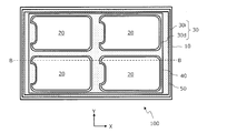
- FIG. 2 is a cross-sectional view of the laminated structure shown in FIG. 1A, taken along line BB. It is a top view which shows the structural example of the resin film in a laminated structure. It is a top view which shows the other structural example of the resin film in a laminated structure. It is sectional drawing which shows the other example of a laminated structure. It is sectional drawing which shows the further another example of a laminated structure. It is sectional drawing which shows typically the division
- FIG. 1 It is a figure which shows typically the state which the stage has supported the laminated structure. It is a figure which shows typically the state which is irradiating the interface of the glass base of a laminated structure, and a resin film with a laser beam (peeling light). It is a perspective view which shows typically a mode that a laminated structure is irradiated with the laser beam (peeling light) radiate
- FIG. 7 is a view schematically showing an example of the configuration of a line beam light source and an example of the light intensity distribution of laser light emitted from a semiconductor laser element during scanning.
- FIG. 7 is a view schematically showing a configuration example of a line beam light source and another example of the light intensity distribution of laser light emitted from a semiconductor laser element during scanning. It is a perspective view which shows typically the other structural example of a line beam light source. It is a figure which shows typically the example of the Y-axis direction distribution of the irradiation intensity of peeling light. It is a figure which shows typically the other example of the Y-axis direction distribution of irradiation intensity of exfoliation light.
- FIG. 5 is a perspective view of a glass base separated from a laminate structure with an LLO device. It is a perspective view which shows the state from which a glass base is removed from a stage. It is a perspective view which shows the state from which the glass base was removed from the stage. It is sectional drawing which shows the state from which the glass base was removed from the stage.
- FIG. 2 is a cross-sectional view showing the flexible OLED device away from the stage.
- FIG. 6 is a cross-sectional view showing another protective sheet fixed to a plurality of OLED devices in contact with a stage. It is sectional drawing which shows the carrier sheet which mounted several components mounted in several OLED devices, respectively.
- FIG. 7 is a process cross-sectional view illustrating a method of manufacturing a flexible OLED device according to an embodiment of the present disclosure.
- FIG. 7 is a process cross-sectional view illustrating a method of manufacturing a flexible OLED device according to an embodiment of the present disclosure.
- FIG. 7 is a process cross-sectional view illustrating a method of manufacturing a flexible OLED device according to an embodiment of the present disclosure.
- FIG. 7 is a process cross-sectional view illustrating a method of manufacturing a flexible OLED device according to an embodiment of the present disclosure. It is an equivalent circuit schematic of one sub pixel in a flexible OLED device. It is a perspective view of the laminated structure in the middle stage of a manufacturing process.
- FIG. 1A and FIG. 1B show an XYZ coordinate system having X, Y, and Z axes orthogonal to one another for reference.
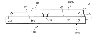
- the laminated structure 100 includes a glass base (mother substrate or carrier) 10, a plurality of functional layer regions 20 each including a TFT layer 20A and an OLED layer 20B, and between the glass base 10 and the plurality of functional layer regions 20.
- a synthetic resin film (hereinafter simply referred to as “resin film”) 30 positioned and fixed to the glass base 10 and a protective sheet 50 covering the plurality of functional layer regions 20 are provided.
- the laminated structure 100 further includes a gas barrier film 40 covering the entire functional layer region 20 between the plurality of functional layer regions 20 and the protective sheet 50.
- the laminated structure 100 may have other layers not shown, such as a buffer layer.
- the first surface 100 a of the laminated structure 100 is defined by the glass base 10, and the second surface 100 b is defined by the protective sheet 50.
- the glass base 10 and the protective sheet 50 are members temporarily used during the manufacturing process, and are not elements constituting the final flexible OLED device.
- the illustrated resin film 30 includes a plurality of flexible substrate regions 30 d respectively supporting the plurality of functional layer regions 20 and an intermediate region 30 i surrounding the individual flexible substrate regions 30 d.
- the flexible substrate region 30d and the intermediate region 30i are only different portions of one continuous resin film 30, and need not be physically distinguished. In other words, in the resin film 30, the portion located immediately below each functional layer region 20 is the flexible substrate region 30d, and the other portion is the intermediate region 30i.
- Each of the plurality of functional layer regions 20 finally constitutes a panel of a flexible OLED device.
- the laminated structure 100 has a structure in which one glass base 10 supports a plurality of flexible OLED devices before division.
- Each functional layer region 20 has, for example, a shape having a thickness (size in the Z-axis direction) of several tens of ⁇ m, a length (size in the X-axis direction) of about 12 cm, and a width (size in the Y-axis direction) of about 7 cm. doing. These sizes can be set to any size depending on the size of the display screen required.
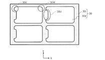
- FIG. 1C is a plan view showing an example of the layout of the flexible substrate region 30 d and the intermediate region 30 i in the resin film 30 in the present embodiment.
- the shape of the respective flexible substrate area 30d comprises a notch 30U, a protrusion 30V, and a curvilinear contour portion 30W.
- the shape of the flexible substrate region 30d is matched to the shape of the flexible OLED device shown in FIG. 1A.
- the flexible OLED device in this embodiment has a shape different from a simple rectangle. This shape is in accordance with the design of electronic devices such as a smartphone, a tablet terminal, a television set and the like on which a flexible OLED device with a narrow frame is mounted as a display device. More specifically, in such an electronic device, components such as a camera, a speaker, and a physical switch can be mounted separately from the display device.
- the notches 30U of the flexible substrate area 30d shown in FIG. 1C can be provided in the area where such components are arranged.
- the plurality of flexible substrate regions 30d are two-dimensionally arranged in rows and columns corresponding to the arrangement of the corresponding flexible OLED devices.
- the intermediate region 30i is composed of a plurality of orthogonal stripes to form a lattice pattern.
- the stripes may include wide portions and narrow portions depending on the uneven shape of the flexible substrate region 30d.
- the width of each stripe in the present embodiment is, for example, about 1 to 10 mm.
- the flexible substrate area 30d of the resin film 30 functions as a "flexible substrate" of the individual flexible OLED devices in the form of the final product.
- the middle region 30i of the resin film 30 is not a component of the final product.
- the configuration of the laminated structure 100 is not limited to the illustrated example.
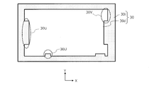
- the number of functional layer regions 20 supported by one glass base 10 does not have to be plural and may be singular.
- the intermediate region 30i of the resin film 30 forms a simple frame pattern surrounding the periphery of one functional layer region 20.
- FIG. 1D is a plan view showing a configuration example of the resin film 30 in the case where the number of OLED devices supported by one glass base 10 is one.
- the shape of the flexible substrate region 30d in this example has a notch 30U and a protrusion 30V.
- the shape of this flexible substrate area 30d is matched to the shape of a flexible OLED device that can be used for a large television or monitor.
- the notch 30U of the flexible substrate area 30d may be provided in an area where components such as a camera, a speaker, and a physical switch are mounted.
- One flexible OLED device of this example may be formed on a glass base 10 having, for example, a size of 1.5 m ⁇ 0.9 m.
- the laminated structure 100 that can be used in the manufacturing method of the present disclosure is not limited to the examples shown in FIGS. 1A and 1B.
- 1E and 1F are cross-sectional views showing other examples of the laminated structure 100, respectively.
- the protective sheet 50 covers the entire resin film 30 and extends outside the resin film 30.
- the protective sheet 50 covers the entire resin film 30 and extends outside the glass base 10. As described later, after the glass base 10 is separated from the laminated structure 100, the laminated structure 100 becomes a flexible thin sheet-like structure having no rigidity.
- the protective sheet 50 impacts the functional layer area 20. And play a role in protecting from friction and the like. Since the protective sheet 50 is finally peeled off from the laminated structure 100, a typical example of the protective sheet 50 has a laminate structure having an adhesive layer (application layer of release agent) with relatively small adhesive force on the surface. doing. A more detailed description of the laminated structure 100 will be described later.
- FIG. 2 is a cross-sectional view schematically showing positions where the middle region 30i of the resin film 30 and the plurality of flexible substrate regions 30d are divided.
- the irradiation position is along the outer periphery of each flexible substrate region 30d.
- a position indicated by an arrow is irradiated with a laser beam for cutting, and a portion other than the glass base 10 in the laminated structure 100 is cut into a plurality of OLED devices 1000 and other unnecessary portions.
- By cutting gaps of several tens of micrometers to several hundreds of micrometers are formed between the individual OLED devices 1000 and their surroundings.
- Such cutting may be performed by a dicing saw instead of the laser beam irradiation.
- FIG. 1 is a cross-sectional view schematically showing positions where the middle region 30i of the resin film 30 and the plurality of flexible substrate regions 30d are divided.
- the irradiation position is along the outer periphery of each flexible substrate region 30d.
- the wavelength of the laser beam may be in any region of infrared, visible light, and ultraviolet. From the viewpoint of reducing the influence of cutting on the glass base 10, a laser beam whose wavelength is included in the green to ultraviolet region is desirable.
- cutting can be performed using the second harmonic (wavelength 532 nm) or the third harmonic (wavelength 343 nm or 355 nm). In that case, if the laser output is adjusted to 1 to 3 watts and scanned at a speed of about 500 mm, the laminate supported on the glass base 10 is not damaged and the OLED device and the unnecessary portion are not damaged. And can be cut (split).
- the timing of performing the above-mentioned cutting is earlier than that of the prior art. Since the cutting is performed in a state where the resin film 30 is fixed to the glass base 10, the cutting alignment can be performed with high accuracy and precision even if the distance between the adjacent OLED devices 1000 is narrow. For this reason, the space between the adjacent OLED devices 1000 can be shortened to reduce the unnecessary portion that is ultimately unnecessary. Moreover, in the prior art, after peeling from the glass base 10, a polarizing plate, a heat dissipation sheet, and / or an electromagnetic shield may be attached so as to cover the entire surface (peeling surface) of the resin film 30.
- the cut also splits the polarizer, the heat dissipation sheet, and / or the electromagnetic shield into a portion covering the OLED device 1000 and other unnecessary portions. Unnecessary parts will be discarded wastefully. On the other hand, according to the manufacturing method of the present disclosure, as described later, the generation of such waste can be suppressed.
- ⁇ Peeling light irradiation> The process of irradiating the interface between the flexible substrate region 30d of the resin film 30 and the glass base 10 with a laser beam with a peeling light irradiation device after dividing the middle region 30i of the resin film 30 and each of the plurality of flexible substrate regions 30d. I do.
- FIG. 3A is a view schematically showing a state immediately before the stage 210 supports the laminated structure 100.
- the stage 210 in the present embodiment is an adsorption stage having a large number of holes for adsorption on its surface.
- the stacked structure 100 is disposed such that the second surface 100 b of the stacked structure 100 faces the surface 210 S of the stage 210, and is supported by the stage 210.
- FIG. 3B is a view schematically showing a state in which the stage 210 supports the laminated structure 100.
- the arrangement relationship between the stage 210 and the laminated structure 100 is not limited to the illustrated example.
- the top and bottom of the stacked structure 100 may be reversed, and the stage 210 may be located below the stacked structure 100.
- the stacked structure 100 is in contact with the surface 210S of the stage 210, and the stage 210 adsorbs the stacked structure 100.
- FIG. 3C is a view schematically showing a state in which the interface between the glass base 10 and the resin film 30 of the laminated structure 100 is irradiated with the peeling light 216 formed in a line shape extending in the direction perpendicular to the paper of FIG. It is.
- a part of the resin film 30 absorbs the peeling light 216 at the interface between the glass base 10 and the resin film 30 and decomposes (disappears).
- the degree of adhesion of the resin film 30 to the glass base 10 is reduced.
- the wavelength of the exfoliation light 216 is typically in the ultraviolet range.
- the wavelength of the peeling light 216 is selected so that the peeling light 216 is hardly absorbed by the glass base 10 and absorbed by the resin film 30 as much as possible.
- the light absorptivity of the glass base 10 can rise to, for example, about 10% in the wavelength region of 343 to 355 nm, and to 30 to 60% at 308 nm.
- the peeling light irradiation apparatus in the present embodiment includes a line beam light source that emits peeling light 216.
- the line beam light source comprises a laser device and a plurality of laser light sources arranged.
- a typical example of the laser light source is a semiconductor laser element (laser diode).
- the peeling light irradiation device is referred to as a “laser lift off (LLO) device”.
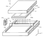
- FIG. 4 is a perspective view schematically showing how the laminated structure 100 is irradiated with the line beam (peeling light 216) emitted from the line beam light source 214 of the LLO apparatus 220 in the present embodiment.
- the stage 210, the stacked structure 100, and the line beam light source 214 are illustrated as being separated in the Z-axis direction in the figure.
- the peeling light 216 is irradiated, the second surface 100 b of the stacked structure 100 is in contact with the stage 210.
- the LLO apparatus 220 illustrated in FIG. 4 includes a moving device 230 for moving the line beam light source 214 so as to move the irradiation position of the line beam in the laminated structure 100 in a direction (scanning direction) intersecting the line beam.
- the illustrated moving device 230 comprises a support 270 and a guide rail 246 which guides the movement of the line beam light source 214.
- the moving device 230 includes an actuator such as a motor, for example, and can move the line beam light source 214.
- the motor may be a rotary electric machine such as a direct current motor, a three-phase alternating current motor, or a stepping motor, or may be a linear motor or an ultrasonic motor. When an ultrasonic motor is used, highly accurate positioning is possible compared to other motors. In addition, since the holding power at the time of stationary is large and can be held without current, heat generation at the time of stationary is small.
- FIG. 5 is a block diagram schematically showing the flow of signals, data and commands in the LLO device 220. As shown in FIG.
- the controller 260 is typically a computer. Some or all of the controller 260 may be a general purpose or special purpose computer system.
- the computer system includes an operating system (OS) and, if necessary, hardware such as peripheral devices.
- OS operating system
- the controller 260 is connected to a memory 274 which is a computer readable recording medium.
- the memory 274 stores a program that defines the operation of the LLO device 220.
- the actual memory 274 may be multiple identical or different types of recording devices.
- One portion of the memory 274 may be non-volatile memory, and the other portion may be random access memory.
- a part or the whole of the memory 274 may be an easily removable optical disc and a solid state recording element, or may be a cloud type storage device on a net stack structure.
- the controller 260 is connected to a sensor 276 such as a temperature sensor and an image sensor. With such a sensor 276, it is possible to detect the irradiation position of the line beam on the laminated structure 100, and to observe the physical or chemical change appearing on the laminated structure 100 by the irradiation.
- a sensor 276 such as a temperature sensor and an image sensor.
- the controller 260 issues an appropriate command to the laser drive circuit (LD drive circuit) 280 and the moving device drive circuit 290 according to the program held in the memory 274 and based on the output of the sensor 276 as necessary.
- the LD drive circuit 280 adjusts the irradiation intensity of the line beam emitted from the line beam light source 214 according to the command of the controller 260.
- Mobile device drive circuit 290 regulates the operation of mobile device 230 in accordance with the command of controller 260.
- the moving device drive circuit 290 controls, for example, the rotational angle and rotational speed of the motor, and adjusts the positional relationship between the line beam light source 214 and the stage 210.
- the line beam light source 214 moves in the X-axis direction with respect to the fixed stage 210 for simplicity, but the LLO apparatus in the present embodiment is not limited to this example.
- the stage 210 may move and the line beam light source 214 may be fixed. Also, both the stage 210 and the line beam source 214 may move in the same or different directions.
- a bearing such as an air slider may be used, for example.
- the line beam light source 214 includes a plurality of arranged semiconductor laser devices, and each semiconductor laser device is connected to a laser diode (LD) drive circuit 280.
- the LD drive circuit 280 receives the electric signal output from the monitoring photodiode described above, and adjusts the light output of the semiconductor laser element to a predetermined level.
- FIG. 6 is a perspective view schematically showing a basic configuration of a semiconductor laser device that can be used for the line beam light source 214.
- the semiconductor laser device 300 shown in FIG. 6 has a semiconductor multilayer structure 322 having an end surface (facet) 326 a including a light emitting region (emitter) 324 for emitting laser light.
- the semiconductor multilayer structure 322 in this example is supported on the semiconductor substrate 320, and includes a p-side cladding layer 322a, an active layer 322b, and an n-side cladding layer 322c.
- a stripe-like p-side electrode 312 is provided on the top surface 326 b of the semiconductor multilayer structure 322.
- An n-side electrode 316 is provided on the back surface of the semiconductor substrate 320.
- a current having a magnitude exceeding the threshold flows in a predetermined region of the active layer 322 b from the p-side electrode 312 to the n-side electrode 316 to cause laser oscillation.
- the end face 326a of the semiconductor multilayer structure 322 is covered by a reflection film (not shown). The laser light is emitted from the light emitting region 324 to the outside through the reflective film.
- the size Ey in the Y-axis direction of the light emitting region 324 is smaller than the size Ex in the X-axis direction. Therefore, the laser beam emitted from the light emitting region 324 spreads in the Y-axis direction due to the diffraction effect. In the embodiments of the present disclosure, this diffraction effect can be used to form a line beam.
- an optical element such as a lens, a diffractive element, or a slit may be disposed in front of the light emitting region 324 to perform beam shaping of the laser light.
- the semiconductor laser device 300 may be formed of various semiconductor materials and may have various structures and sizes depending on the oscillation wavelength and the light output.
- the semiconductor multilayer structure 322 of the semiconductor laser device 300 can be suitably formed of an AlGaN-based or InAlGaN-based nitride semiconductor.
- the oscillation wavelength of the semiconductor laser device 300 can be set, for example, in the range of 200 nm to 350 nm.
- a ridge stripe may be provided in the p-side cladding layer 322a to perform horizontal horizontal light confinement.
- the active layer 322 b may include one or more quantum well structures.
- the semiconductor stack structure 322 may include other semiconductor layers such as light guide layers, buffer layers, and contact layers.
- the n-side electrode 316 is disposed on the side of the substrate 320 where the p-side electrode 312 is provided.
- the configuration shown in FIG. 6 is only a typical example of the configuration of the semiconductor laser device 300, and is simplified to simplify the description. This simplified configuration example does not limit the embodiments of the present disclosure in any way. It is also possible to form a line beam using a surface emitting semiconductor laser element. In the other drawings, the description of components such as the n-side electrode 316 may be omitted for the sake of simplicity.
- the line beam light source 214 includes a plurality of semiconductor laser devices 300 and a plurality of supports 214 A for supporting the semiconductor laser devices 300.
- the semiconductor laser device 300 and the support 214A are housed inside the housing 214B.
- the support 214A is preferably formed of a good conductor having high thermal conductivity, for example, a metal such as copper or a ceramic material such as aluminum nitride.
- the inside of the housing 214B can be shielded from the atmospheric atmosphere by closing the housing 214B with, for example, a translucent cover (not shown).
- the inside of the housing 214 B is filled with, for example, a gas inert to the semiconductor laser device 300.
- thermoelectric cooling device such as a Peltier device may be arranged in the vicinity of the semiconductor laser device 300.
- the support 214A may be provided with an internal channel for water cooling and fins for air cooling.
- a photodiode (not shown) is disposed in the vicinity of an end face 326 c located on the side opposite to the end face 326 a on the emission side of each semiconductor laser device 300.
- the end face 326c is covered with a reflective film having a relatively high reflectance, but a part of the laser beam oscillating inside the semiconductor laser device 300 leaks from the end face 326c to the outside.
- the intensity of the laser light emitted from the end face 326a can be monitored.
- the output of the photodiode is used for power control as described above.
- eleven semiconductor laser devices 300 are arranged along the same line parallel to the Y axis.
- the number of semiconductor laser devices 300 is not limited to this example, and may be 10 or less, or 12 or more.
- 50 or more than 100 semiconductor laser elements 300 are arranged in the same line. It can be done.
- Each semiconductor laser device 300 can have the same configuration as the semiconductor laser device 300 of FIG.
- the laser light (peeling light 216) emitted from each light emitting area 324 of the semiconductor laser device 300 spreads in parallel to the same line to form a line beam.
- FIG. 7A schematically shows a rectangular scanning surface SC parallel to the XY plane, and an irradiation area 218 where laser light (peeling light 216) is formed on the scanning surface SC.
- the scanning surface SC corresponds to the interface between the resin film 30 and the glass base 10 in the laminated structure 100.
- FIG. 7A shows, for reference, the distribution in the X-axis direction of the irradiation intensity IS in the irradiation area 218 at a certain time and the distribution in the Y-axis direction.
- the distribution in the X-axis direction of the irradiation intensity IS is narrow and exhibits unimodality.
- the distribution in the Y-axis direction of the irradiation intensity IS has eleven peaks because the laser beams emitted from the eleven semiconductor laser elements 300 overlap and extend in a line shape. .
- the laser beams emitted from the individual semiconductor laser devices 300 tend to spread in a predetermined direction (in this example, the Y-axis direction) due to the diffraction effect.
- This property is suitable for forming a line beam extending in the Y-axis direction.
- an optical element such as a cylindrical lens may be used in order to suppress the spread in the X-axis direction and increase the irradiation energy per second (per unit area joule / cm 2 ) per unit area.
- the width (size in the X-axis direction) of the irradiation area 218 on the scanning surface SC can be narrowed to, for example, about 0.2 mm or less.
- the arrangement pitch of the semiconductor laser devices 300 it is preferable to reduce the arrangement pitch of the semiconductor laser devices 300 to increase the number density of the semiconductor laser devices 300.
- 100 or more semiconductor laser elements 300 may be linearly arranged at intervals of 1 mm to 5 mm (arrangement pitch: distance between centers of adjacent light sources).
- the irradiation intensity can be modulated with high spatial resolution of, for example, 1 mm to 5 mm. It will be possible.
- an optical element optical system for collimating or focusing
- FIG. 7B shows a state in which the line beam light source 214 is translated in the positive direction of the X axis from the position shown in FIG. 7A.
- the irradiation area 218 also translates with the movement of the line beam light source 214.
- the output of each semiconductor laser device 300 is lowered compared to the state of FIG. 7A.
- the output of each semiconductor laser device 300 need not be increased or decreased at the same timing. In other words, not only the distribution in the X-axis direction of the irradiation intensity IS but also the distribution in the Y-axis direction can be changed variously during scanning of the line beam.
- the output of the semiconductor laser device 300 can be temporally and / or spatially modulated according to the position of the irradiation region 218. Therefore, the distribution of the irradiation intensity on the scan surface SC can be controlled.
- FIG. 8 is a perspective view showing another configuration example of the line beam light source 214 provided with a plurality of semiconductor laser devices 300.
- the two rows of semiconductor laser devices 300 have a stagger pattern (staggered arrangement). It is also possible to form a single line beam as a whole by shortening the center-to-center distance of the two rows. Further, the orientation of the semiconductor laser device 300 is adjusted such that the optical axis of the semiconductor laser device 300 belonging to the first row and the optical axis of the semiconductor laser device 300 belonging to the second row intersect on the laminated structure 100. If so, substantially one line beam can be formed.
- the irradiation area of the peeling light does not have to be a single line, and the irradiation areas are distributed continuously or discontinuously in the direction intersecting the scanning direction. Just do it.
- the line beam light source may be provided with a plurality of light sources arranged along the line. Also, the number of such lines is not limited to one, and may be two or more.
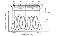
- FIG. 9 is a view schematically showing an example of the Y-axis direction distribution of the irradiation intensity of the peeling light 216.
- the horizontal axis of the graph in FIG. 9 indicates the Y-axis coordinate value of the irradiation area, and the vertical axis indicates the irradiation intensity.
- the unit of irradiation intensity is indicated by the energy density per unit area (for example, [mJ / cm 2 ]).
- specific numerical values of the irradiation intensity are not described.
- Irradiation intensity indicates the value of for example 0 mJ / cm 2 or more 500 mJ / cm 2 within the following ranges.
- a curve indicated by a broken line in the graph in FIG. 9 indicates the distribution I (Y) of the irradiation intensity in the Y-axis direction.
- the Y-axis direction distribution I (Y) of the irradiation intensity is defined by the superposition of the light intensity distributions of the laser beams emitted from the plurality of semiconductor laser devices 300 (such as FIG. 7A) of the line beam light source 214.
- the light intensity distribution of the laser light emitted from each semiconductor laser device 300 can be shaped using an optical element such as a lens.
- the illustrated light intensity distribution is merely an example.
- the straight line of the dashed-dotted line in FIG. 9 has shown threshold value level Th of the irradiation intensity required for peeling.
- the threshold level Th is, for example, 250 to 300 mJ / cm 2 .
- the amount of absorption of peeling light by the resin film 30 is insufficient, and the resin film 30 in that region is fixed without peeling from the glass base 10 Maintain the condition.
- a cross section of the laminated structure 100 parallel to the YZ plane is shown above the graph in FIG. 9 for reference.
- the glass base 10 extends from the position Y0 to the position Y5.
- the left OLED device 1000 is in the area from position Y1 to position Y2, and the right OLED device 1000 is in the area from position Y3 to position Y4.
- the flexible substrate area 30d of the resin film 30 corresponds to the area from the position Y1 to the position Y2 and the area from the position Y3 to the position Y4.
- the intermediate region 30i of the resin film 30 corresponds to the region from the position Y0 to the position Y1, the region from the position Y2 to the position Y3, and the region from the position Y4 to the position Y5.
- the irradiation intensity distribution I (Y) of the separation light exceeds the threshold level Th in the area from the position Y1 to the position Y2 and the area from the position Y3 to the position Y4.
- the interface between the flexible substrate region 30 d of the resin film 30 and the glass base 10 is irradiated with the peeling light of the irradiation intensity exceeding the threshold level Th.
- the irradiation intensity distribution I of the peeling light (Y) is lower than the threshold level Th Contains parts.
- the lowest value indicated by the irradiation intensity distribution I (Y) of the peeling light during scanning is typically 0 mJ / cm 2 , but if it is lower than the threshold level Th, even a value exceeding 0 mJ / cm 2 Good.
- the irradiation intensity distribution be uniform.
- the irradiation intensity of the line beam does not need to be uniform as long as the irradiation intensity of the peeling light at the interface requiring the peeling exceeds the threshold level Th.
- the irradiation intensity distribution I (Y) of the separation light has a large number of peaks, but the embodiment of the present disclosure is not limited to such an example.
- a part of the irradiation intensity distribution I (Y) of the separation light may be linear.
- the light intensity distribution of the laser light output from the individual semiconductor laser devices 300 (such as FIG. 7A) of the line beam light source 214 is a flat “top hat” type centered on the respective optical axes.
- the irradiation intensity of the separation light at the interface that needs to be separated exceeds the threshold level Th, the irradiation intensity of the line beam does not need to be uniform. Therefore, the light outputs of the plurality of semiconductor laser devices 300 may be different from one another.
- the irradiation intensity of the laser light with respect to the interface between the intermediate region 30i of the resin film 30 and the glass base 10 in the irradiation intensity distribution I (Y) is set to the flexible substrate region 30d of the resin film 30 and the glass base 10. Lower than the irradiation intensity of the laser light to the interface of
- FIG. 11 shows an example of the Y-axis direction distribution I (Y) in a cross section different from the Y-axis direction distribution I (Y) shown in FIG.
- This cross section is a cross section across the protrusion 30V and the notch 30U of the flexible substrate region 30d shown in FIG. 1C.
- the center of each of the two OLED devices 1000 includes the middle region 30i of the resin film 30 and a portion to be fixed to the glass base 10 without being peeled off from the glass base 10.
- the Y-axis direction distribution I (Y in the interface between the intermediate region 30i of the resin film 30 and the glass base 10).
- the threshold level Th Locally below the threshold level Th.
- the portion corresponding to the notch 30U of the flexible substrate region 30d forms a "wide portion" in the stripe-shaped "low irradiation region".
- FIG. 12 shows another example of the Y-axis direction distribution I (Y) in the same cross section as the cross section in FIG.
- the Y-axis direction distribution I (Y) in FIG. 12 can be realized by a line beam light source 214 in which 27 or more semiconductor laser devices are arrayed.
- the laser beams emitted from the individual semiconductor laser elements can realize Y-axis direction distribution I (Y) which changes with higher spatial resolution as compared with the example of FIG.
- the irradiation intensity may be zero at the interface between the intermediate region 30i of the resin film 30 and the glass base 10.
- the line beam light source 214 includes a plurality of laser light sources, it is possible to spatially and temporally modulate the irradiation intensity in the line beam by adjusting the outputs of the individual laser light sources. . For this reason, spatial distribution of the irradiation intensity according to the shape of the OLED device 1000 which the laminated structure 100 has, size, and arrangement
- positioning is easily realizable. More specifically, by temporally changing the spatial distribution of the irradiation intensity in the line beam during scanning, peeling is performed, for example, on a flexible substrate region 30d having a shape as shown in FIG. 1C or FIG. 1D.
- the peeling light can be irradiated with the irradiation intensity required for the irradiation, and the peeling light can be irradiated with the irradiation intensity that does not cause peeling to the intermediate region 30i of the resin film 30.
- the peeling light can be irradiated with the irradiation intensity required for the irradiation, and the peeling light can be irradiated with the irradiation intensity that does not cause peeling to the intermediate region 30i of the resin film 30.
- flexible response is possible.
- the region for lowering the irradiation intensity of the peeling light below the level required for peeling does not have to be the entire middle region 30i of the resin film 30. If a part of the intermediate region 30i of the resin film 30 is fixed to the glass base 10, the entire unnecessary part of the laminated structure 100 can be left on the glass base 10. According to the embodiment of the present disclosure, it becomes easy to leave the unnecessary portion of the laminated structure 100 on the glass base 10 in a wide range according to the shape.
- the typical example of a laser light source is a semiconductor laser element
- embodiment of this indication is not limited to this example.
- a semiconductor laser device When a semiconductor laser device is used, there is an advantage that a small and lightweight line beam light source can be realized.
- each of the plurality of laser light sources is a laser device larger than the semiconductor laser device.
- the oscillation wavelength of the laser light source is out of the range suitable for peeling of the resin film, it may be converted to a harmonic by a wavelength conversion element and used.
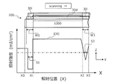
- FIG. 13 is a view schematically showing an example of the X-axis direction (scanning direction) distribution of the irradiation intensity of the peeling light 216.
- the horizontal axis of the graph in FIG. 13 indicates the X-axis coordinate value of the irradiation position, and the vertical axis indicates the irradiation intensity.
- the solid line in the graph in FIG. 13 indicates the distribution I (X) of the irradiation intensity in the X-axis direction.
- the straight line of the dashed dotted line indicates the threshold level Th of the irradiation intensity required for the separation.
- a cross section of the laminated structure 100 parallel to the XZ plane is shown above the graph in FIG. 13 for reference.
- This cross section is in a relation orthogonal to the cross section of FIG.
- the glass base 10 extends from the position X0 to the position X5.
- the OLED device 1000 on the left side in the figure is in the region from position X1 to position X2, and the OLED device 1000 on the right side is in the region from position X3 to position X4.
- the flexible substrate region 30d of the resin film 30 corresponds to the region from the position X1 to the position X2 and the region from the position X3 to the position X4.
- intermediate region 30i of resin film 30 is a region from position X0 to position X1 (width: W1), a region from position X2 to position X3 (width: W3), and a region from position X4 to position X5 Width: corresponds to W3).
- a region (width: S1) in which the irradiation intensity is lower than the threshold level Th is formed in the middle region 30i (width: W1) located at the left end of the resin film 30 in FIG. 13 a region (width: S1) in which the irradiation intensity is lower than the threshold level Th is formed.
- another region (width: S2) in which the irradiation intensity is lower than the threshold level Th is formed in the (width: W2) of the middle region 30i located at the right end of the resin film 30 in FIG.
- W1> S1 and W2> S2 are established.
- the width S1 is preferably 50% or more of the width W1
- the width S2 is preferably 50%
- the X-axis direction distribution I (X) of the irradiation intensity indicates the entire scan (sum or integral value) of the separation light. For example, when the irradiation position of the peeling light (the position of the center line of the line beam) is moved from the position X0 to the position X1, the region from the position X1 to the position X5 is not irradiated with the peeling light, and the position X1 at that time The irradiation intensity of the separation light in the region from the point X to the position X5 is naturally zero.
- the line width (short axis dimension, size in the X-axis direction) of the peeling light 216 may be, for example, about 0.2 mm. This dimension defines the size of the irradiation area at the interface between the resin film 30 and the glass base 10 at a certain time.
- Exfoliation light 216 may be illuminated as a pulsed or continuous wave. The pulsed irradiation can be performed, for example, at a frequency of about 200 times per second (the number of shots per second). In the case of using the pulsed peeling light 216, the scanning speed is determined so that the irradiation area partially overlaps in two successive shots.
- the line width (minor axis dimension, size in the X-axis direction) of the peeling light 216 is 0.2 mm
- gaps may occur between each shot.
- more than 100 shots per second are required.
- the positioning accuracy of the irradiation position depends on the mechanical feeding accuracy of the line beam light source 214.
- the line width (minor axis dimension, size in the X-axis direction) of the exfoliation light 216 is 40 ⁇ m, for example, the line beam light source 214 is moved stepwise by 20 ⁇ m to overlap the irradiation area by two consecutive shots. The amount can be 50%.
- the overlap amount of the irradiation area by two consecutive shots can be made 75%.
- the irradiation of the peeling light may be performed when the relative movement of the line beam light source 214 with respect to the stage 210 is stopped. It is easy to adjust the irradiation intensity to a target value as compared with irradiating a moving object with laser light to irradiate the stopped object with laser light. For example, the irradiation intensity can be adjusted by increasing or decreasing the number of irradiation pulses or the irradiation time at the stop position. Further, according to the embodiment of the present disclosure, since the semiconductor laser device is used as the light source, there is also an advantage that the oscillation state of the semiconductor laser device can be adjusted to easily control the irradiation intensity.
- the irradiation intensity can be modulated by increasing or decreasing the number of shots per second. Conversely, when the number of shots per second is fixed, the irradiation intensity can be modulated by increasing or decreasing the moving speed (scanning speed) of the irradiation position. It is also possible to modulate the illumination intensity by changing other parameters, such as, for example, the optical distance from the line beam light source 214 to the laminated structure 100. A mechanical shutter is disposed between the line beam light source 214 and the glass base 10, and even if the light path of the peeling light is blocked by this shutter, it is possible to form a low illumination area.
- the irradiation intensity of the peeling light to at least a part of the interface between the intermediate region 30i of the resin film 30 and the glass base 10 is the same as that of the flexible substrate region 30d of the resin film 30 and the glass base 10 Is lower than the irradiation intensity of the peeling light to the interface of
- This "at least part of" area may be referred to as a "low radiation area” or a "non-peeling area".
- the low illumination area includes two parallel stripe areas (area of width S1 and area of width S2) extending along the outer edge of the glass base 10.
- the two stripe regions can be formed respectively by the irradiation of the weak exfoliation light 216 shown in FIGS. 5A and 5D. In the two stripe regions, since the irradiation intensity of the peeling light 216 is lower than the threshold level Th, the intermediate region 30i of the resin film 30 remains fixed to the glass base 10.
- any of the stripe regions defining the “low irradiation utilization region” may have a wide portion and / or a narrow portion corresponding to the middle region 30i of the resin film 30.
- FIG. 14 shows an example in which the irradiation intensity is temporarily made lower than the threshold level Th in the middle of the scanning of the separation light 216.
- the irradiation intensity is lower than the threshold level Th in a part of the area from the position X2 to the position X3 (width: S3).
- the “low radiation area” at the interface between the middle area 30i of the resin film 30 and the glass base 10 is one middle stripe area (width: S3) parallel to two stripe areas in addition to the two stripe areas. Contains.
- the widths S1, S2, and S3 of these stripe regions are all, for example, 1 mm or more, and in one example, 3 mm or more.
- two OLED devices 1000 are arranged along the direction of the X-axis.
- N OLED devices 1000 are arranged along the direction of the X axis, where N is an integer of 3 or more, the total number of stripes formed by intermediate regions 30i sandwiched between two adjacent OLED devices 1000 is N. It is -1. It is not necessary to provide low illumination areas on all N-1 stripes. In addition, a plurality of low radiation areas may be provided for the middle area 30i constituting one stripe.
- FIGS. 15A and 15B are diagrams schematically showing still another example of the X-axis direction distribution of the irradiation intensity of the peeling light.
- the modulation pattern of the irradiation intensity at the interface between the intermediate region 30i surrounding the OLED device 1000 located on the left side of FIG. 13 and the glass base 10 is illustrated.
- the stripe-shaped low irradiation region (width: S1) extending along the outer edge of the resin film 30 does not reach the outer edge of the resin film 30.
- the irradiation intensity of the peeling light may exceed the threshold level Th before the peeling light irradiates the glass base 10.
- the irradiation intensity may gradually change.
- the width (the size in the scanning direction) of the “low irradiation region” can be defined as the width of the region where the irradiation intensity is lower than the threshold level Th.
- the low radiation region is constituted by a plurality of relatively narrow stripes.
- Such a low irradiation area can be realized, for example, when irradiating pulsed peeling light so that the irradiation areas do not overlap between successive shots.
- the irradiation intensity in “at least a part thereof” is lower than the threshold level Th. It is desirable to do. However, even when not lower than the threshold level Th, the intermediate region 30i tends to remain on the glass base 10 by achieving the irradiation intensity lower than the irradiation intensity in the region to be peeled off. If the difference between the irradiation intensity in the region to be peeled off and the irradiation intensity in the low irradiation region is 50 mJ / cm 2 or more, a sufficient effect can be obtained.
- the peeling light is a line beam extending in a direction (first direction) parallel to the outer edge of the glass base 10, and the scanning direction is a second direction orthogonal to the first direction.
- first direction and the second direction do not have to be orthogonal to each other as long as they intersect.
- the irradiation position of the peeling light is moved (scanned) by moving the position of the line beam light source 214 with respect to the fixed stage 210.
- the line beam light source 214 may be fixed and the stage 210 may be moved to perform the stripping light removal.
- the ablation light may be scanned by moving both the line beam light source 214 and the stage 210.
- FIG. 16A describes a state in which the laminated structure 100 is in contact with the stage 210 after the irradiation of the peeling light. While maintaining this state, the distance from the stage 210 to the glass base 10 is enlarged. At this time, the stage 210 in the present embodiment adsorbs the OLED device portion of the laminated structure 100.
- the drive holds the glass base 10 and moves the whole of the glass base 10 in the direction of the arrow L to perform peeling (lift off).
- the glass base 10 can move together with the adsorption stage while being adsorbed by the adsorption stage (not shown).
- the direction of movement of the glass base 10 need not be perpendicular to the first surface 100 a of the laminated structure 100 but may be inclined.
- the movement of the glass base 10 need not be a linear movement, but may be a rotational movement.
- the glass base 10 may be fixed by a holding device (not shown) or another stage, and the stage 210 may move upward in the figure.
- FIG. 16B is a cross-sectional view showing the first portion 110 and the second portion 120 of the laminated structure 100 separated in this manner.
- FIG. 17 is a perspective view showing the second portion 120 of the laminated structure 100.
- the first portion 110 of the laminated structure 100 includes a plurality of OLED devices 1000 in contact with the stage 210.
- Each OLED device 1000 has a functional layer region 20 and a plurality of flexible substrate regions 30 d of the resin film 30.
- the second portion 120 of the laminated structure 100 has the glass base 10 and the intermediate region 30i of the resin film 30.
- the middle region 30i of the resin film 30 is fixed to the glass base 10 in at least a part of the low radiation region. Therefore, the entire intermediate region 30i of the resin film 30 adheres to the glass base 10 and is separated from the stage 210 in a state.
- both the exfoliation light irradiation process and the exfoliation process are performed by the LLO apparatus 220 equipped with the stage 210.
- Embodiments of the present disclosure are not limited to such examples.
- the irradiation process of separation light is performed by a separation light irradiation apparatus including a stage 210, and the separation process may be performed using another apparatus including another stage different from the stage 210. In this case, it is necessary to move the laminated structure 100 from the stage 210 to another stage (not shown) after the irradiation of the peeling light. If both the irradiation process and the peeling process of the peeling light are performed using the same stage, the process of moving the laminated structure between the stages can be omitted.
- the stage 210 adsorbs the second surface 100 b of the stacked structure 100.
- the cutting step shown in FIG. 2 that is, the step of cutting a portion other than the glass base 10 in the laminated structure 100 into a plurality of OLED devices 1000 and other unnecessary portions is before irradiation with peeling light.
- performing the cutting process before the exfoliation light irradiation process is effective to realize the separation shown in FIGS. 16B and 17.
- the irradiation intensity of the peeling light is modulated so that a part of the unnecessary portion adheres to the glass base 10.
- FIG. 18 shows a first portion 110 (OLED device 1000) of the laminated structure 100 in a state of being adsorbed to the stage 210, and a second portion 120 (glass base 10 and deposit) located away from the stage 210.
- FIG. 10 unnecessary portions that do not constitute the OLED device 1000 are attached to the glass base 10.
- FIG. 19 is a perspective view showing a first portion 110 of the laminated structure 100 in a state of being adsorbed to the stage 210.
- the first portion 110 of the stacked structure 100 supported by the stage 210 is a plurality of OLED devices 1000 arranged in rows and columns.
- the surface (peeling surface) 30s of the flexible substrate region 30d in the resin film 30 is exposed.
- the OLED device 1000 and the flexible substrate region 30 d of the resin film 30 functioning as the flexible substrate thereof have a complicated planar shape as shown in FIG.
- the 1000 can be properly separated from other unwanted parts. This is necessary to selectively peel the flexible substrate region 30d of the resin film 30 by temporally changing the spatial distribution of the irradiation intensity of the peeling light when scanning the peeling light as described above. It is realized by giving various irradiation intensity.
- the intermediate region 30i of the resin film 30 can also be maintained in a state in which the entire region thereof is fixed to the glass base 10.
- FIG. 20 is a cross-sectional view showing the stage 210 adsorbing the OLED device 1000. This cross section is a cross section parallel to the ZX plane. The direction of the Z-axis in FIG. 20 is reversed from the direction of the Z-axis in FIGS. 18 and 19.
- Processing for the OLED device 1000 is to apply a film of dielectric and / or conductor to each of the plurality of OLED devices 1000, to perform cleaning or etching, and to mount optical components and / or electronic components. Can be included. Specifically, components such as, for example, a polarizing plate, a sealing film, a touch panel, a heat dissipation sheet, an electromagnetic shield, and a driver integrated circuit may be mounted on the flexible substrate region 30d of the individual OLED device 1000. Sheet-like components include functional films that can add optical, electrical, or magnetic functions to the OLED device 1000.
- the surface 30s of the resin film 30 peeled off from the glass base 10 is active, so after covering the surface 30s with a protective film or performing surface treatment for hydrophobization, various components are mounted thereon. It is also good.
- FIG. 21 is a cross-sectional view schematically showing a state in which the OLED device 1000 is removed from the stage 210 after the sheet-like component (functional film) 60 is mounted.
- the individual OLED devices 1000 may be sequentially or At the same time, it becomes possible to execute various processes efficiently.
- the step of fixing the protective sheet 70 may be further performed.
- the second protective sheet 70 can exhibit a function of temporarily protecting the surface of the flexible substrate region 30 d of the resin film 30 peeled off from the glass base 10.
- the second protective sheet 70 may have the same laminate structure as the above-described protective sheet 50.
- the protective sheet 50 can be referred to as a first protective sheet 50.
- the second protective sheet 70 may be fixed to the plurality of OLED devices 1000 after performing the various processes described above on each of the plurality of OLED devices 1000 in contact with the stage 210.
- the second protective sheet 70 After the second protective sheet 70 is attached, when the adsorption by the stage 210 on the OLED device 1000 is stopped, the plurality of OLED devices 1000 fixed to the second protective sheet 70 can be separated from the stage 210. Thereafter, the second protective sheet 70 may function as a carrier of the plurality of OLED devices 1000. This is the transfer of the OLED device 1000 from the stage 210 to the second protective sheet 70. Various treatments may be performed on each of the plurality of OLED devices 1000 in a state of being fixed to the second protective sheet 70 sequentially or simultaneously.
- FIG. 23 is a cross-sectional view showing a carrier sheet 90 on which a plurality of components (functional films) 80 mounted on a plurality of OLED devices 1000 are mounted.
- Each component 80 can be attached to the OLED device 1000 by moving such a carrier sheet 90 in the direction of arrow U.
- the top surface of the component 80 has an adhesive layer that strongly adheres to the OLED device 1000.
- the carrier sheet 90 and the part 80 are relatively weakly attached.
- collective “transfer" of the component 80 is possible. Such transfer is easily achieved because the plurality of OLED devices 1000 are supported regularly at the stage 210.
- FIG. 24A is a cross-sectional view showing a glass base 10 having a resin film 30 formed on its surface.
- the glass base 10 is a support substrate for a process, and its thickness may be, for example, about 0.3 to 0.7 mm.
- the resin film 30 in the present embodiment is, for example, a polyimide film having a thickness of 5 ⁇ m to 100 ⁇ m.
- the polyimide film can be formed from a precursor polyamic acid or polyimide solution. After forming a film of polyamic acid on the surface of the glass base 10, thermal imidization may be performed, or a film may be formed on the surface of the glass base 10 from a polyimide solution in which polyimide is melted or dissolved in an organic solvent.
- the polyimide solution can be obtained by dissolving a known polyimide in any organic solvent. After applying the polyimide solution to the surface 10s of the glass base 10, a polyimide film can be formed by drying.
- the polyimide film realize high transmittance throughout the visible light region.
- the transparency of the polyimide film can be expressed, for example, by the total light transmittance according to JIS K 7105-1981.
- the total light transmittance may be set to 80% or more, or 85% or more.
- the transmittance is not affected.
- the resin film 30 may be a film formed of a synthetic resin other than polyimide. However, in the embodiment of the present disclosure, since the heat treatment is performed, for example, at 350 ° C. or more in the process of forming the thin film transistor, the resin film 30 is formed of a material that does not deteriorate by this heat treatment.
- the resin film 30 may be a laminate of a plurality of synthetic resin layers.
- laser lift-off is performed in which the resin film 30 is irradiated with ultraviolet laser light that transmits the glass base 10.
- a part of the resin film 30 needs to absorb and decompose (disappear) such ultraviolet laser light at the interface with the glass base 10.
- a sacrificial layer (a thin layer made of metal or amorphous silicon) that absorbs laser light in a certain wavelength range and generates gas may be disposed between the glass base 10 and the resin film 30.
- the resin film 30 can be easily peeled off from the glass base 10 by the irradiation of the laser light.
- Providing the sacrificial layer also has the effect of suppressing the formation of ash.
- ⁇ Polishing treatment> When a polishing target (target) such as particles or protrusions is present on the surface 30x of the resin film 30, the target may be polished and planarized by a polishing apparatus. The detection of any foreign matter in the particles is possible, for example, by processing the image acquired by the image sensor. After the polishing process, the surface 30x of the resin film 30 may be planarized.
- the planarization process includes the step of forming a film (planarization film) for improving flatness on the surface 30 x of the resin film 30.
- the planarization film does not have to be made of resin.
- a gas barrier film may be formed on the resin film 30.
- the gas barrier film can have various structures.
- An example of the gas barrier film is a film such as a silicon oxide film or a silicon nitride film.
- Another example of the gas barrier film may be a multilayer film in which an organic material layer and an inorganic material layer are laminated. This gas barrier film may be called “lower layer gas barrier film” to distinguish it from the gas barrier film described later covering the functional layer region 20.
- region 20 can be called "upper layer gas barrier film.”
- a plurality of functional layer regions 20 are formed on the glass base 10.
- a resin film 30 fixed to the glass base 10 is located between the glass base 10 and the functional layer region 20.
- the functional layer region 20 includes the TFT layer 20A located in the lower layer and the OLED layer 20B located in the upper layer.
- the TFT layer 20A and the OLED layer 20B are sequentially formed by a known method.
- the TFT layer 20A includes a circuit of a TFT array that realizes an active matrix.
- the OLED layer 20B includes an array of OLED elements that can each be driven independently.
- the thickness of the TFT layer 20A is, for example, 4 ⁇ m, and the thickness of the OLED layer 20B is, for example, 1 ⁇ m.
- FIG. 25 is a basic equivalent circuit diagram of a sub pixel in an organic EL (Electro Luminescence) display.
- One pixel of the display may be constituted by sub-pixels of different colors such as, for example, R (red), G (green), B (blue).
- the example shown in FIG. 25 includes the selection TFT element Tr1, the driving TFT element Tr2, the holding capacitance CH, and the OLED element EL.
- the selection TFT element Tr1 is connected to the data line DL and the selection line SL.
- the data line DL is a wire carrying a data signal that defines an image to be displayed.
- the data line DL is electrically connected to the gate of the driving TFT element Tr2 through the selecting TFT element Tr1.
- the selection line SL is a wire carrying a signal for controlling on / off of the selection TFT element Tr1.
- the driving TFT element Tr2 controls the conduction state between the power line PL and the OLED element EL.
- a current flows from the power line PL to the ground line GL through the OLED element EL. This current causes the OLED element EL to emit light.
- the selection TFT element Tr1 is turned off, the on state of the driving TFT element Tr2 is maintained by the storage capacitor CH.
- the TFT layer 20A includes a selection TFT element Tr1, a drive TFT element Tr2, a data line DL, a selection line SL, and the like.
- the OLED layer 20B includes an OLED element EL. Before the OLED layer 20B is formed, the upper surface of the TFT layer 20A is planarized by an interlayer insulating film covering the TFT array and various wirings.
- the structure that supports the OLED layer 20B and implements active matrix driving of the OLED layer 20B is referred to as a "backplane".
- Portions of the circuit elements and the wirings shown in FIG. 25 can be included in any of the TFT layer 20A and the OLED layer 20B.
- the wiring shown in FIG. 25 is connected to a driver circuit (not shown).
- specific configurations of the TFT layer 20A and the OLED layer 20B may vary. These configurations do not limit the content of the present disclosure.
- the configuration of the TFT element included in the TFT layer 20A may be a bottom gate type or a top gate type. Further, light emission of the OLED element included in the OLED layer 20B may be bottom emission type or top emission type.
- the specific configuration of the OLED element is also optional.
- the material of the semiconductor layer constituting the TFT element includes, for example, crystalline silicon, amorphous silicon, and an oxide semiconductor.
- part of the process of forming the TFT layer 20A includes a heat treatment process at 350 ° C. or higher.
- the entire functional layer region 20 is covered with the gas barrier film (upper gas barrier film) 40 as shown in FIG. 24C.
- a typical example of the upper gas barrier film 40 is a multilayer film in which an inorganic material layer and an organic material layer are laminated.
- An adhesive film, another functional layer constituting a touch screen, a polarizing film, or the like may be disposed between the upper gas barrier film 40 and the functional layer region 20, or on the upper layer of the upper gas barrier film 40.
- the upper gas barrier film 40 can be formed by thin film encapsulation (TFE) technology.
- the WVTR Water Vapor Transmission Rate
- the WVTR Water Vapor Transmission Rate of the thin film sealing structure is typically required to be 1 ⁇ 10 ⁇ 4 g / m 2 / day or less. This criterion is achieved according to the embodiments of the present disclosure.
- the thickness of the upper gas barrier film 40 is, for example, 1.5 ⁇ m or less.
- FIG. 26 is a perspective view schematically showing the upper surface side of the laminated structure 100 at the stage when the upper gas barrier film 40 is formed.
- One laminated structure 100 includes a plurality of OLED devices 1000 supported by a glass base 10.
- one stacked structure 100 includes more functional layer regions 20 than the example shown in FIG. 1A. As described above, the number of functional layer regions 20 supported by one glass base 10 is arbitrary.
- a protective sheet 50 is attached to the top surface of the laminated structure 100.
- the protective sheet 50 may be formed of, for example, a material such as polyethylene terephthalate (PET) or polyvinyl chloride (PVC).
- PET polyethylene terephthalate
- PVC polyvinyl chloride
- the typical example of the protective sheet 50 has a laminate structure having a coated surface of a release agent.
- the thickness of the protective sheet 50 may be, for example, 50 ⁇ m or more and 200 ⁇ m or less.
- the manufacturing method according to the present disclosure can be performed using the above-described manufacturing apparatus (LLO apparatus 220).
- Embodiments of the present invention provide a method of fabricating a new flexible OLED device.
- Flexible OLED devices can be widely applied to smartphones, tablet terminals, automotive displays, and small to large sized television devices.
Landscapes
- Engineering & Computer Science (AREA)
- Theoretical Computer Science (AREA)
- Manufacturing & Machinery (AREA)
- Computer Hardware Design (AREA)
- Physics & Mathematics (AREA)
- General Physics & Mathematics (AREA)
- Human Computer Interaction (AREA)
- General Engineering & Computer Science (AREA)
- Electroluminescent Light Sources (AREA)
- Devices For Indicating Variable Information By Combining Individual Elements (AREA)
Abstract
La présente invention concerne un procédé de production de dispositifs DELO flexibles consistant à séparer une région de carte de base flexible (30d) d'une région intermédiaire (30i) d'un film de résine (30) d'un corps à structure en couches (100), puis à exposer la limite entre la région de carte de base flexible (30d) et la base en verre (10) à un rayonnement de lumière laser ; et, dans un état dans lequel le corps à structure en couches (100) est en contact avec une platine (210), à séparer le corps à structure en couches (100) en une première partie (110) et une seconde partie (120). La première partie (110) contient une pluralité de dispositifs DELO (1000) en contact avec la platine (210), chacun des dispositifs DELO (1000) comportant une pluralité de régions de couche fonctionnelle (20) et la région de carte de base flexible (30d). La seconde partie (120) contient la base en verre (10) et la région intermédiaire (30i). L'étape d'exposition au rayonnement de lumière laser comprend les étapes consistant à : former la lumière laser à l'aide d'une pluralité de sources de lumière laser qui ont été disposées en réseau ; moduler temporellement et spatialement les sorties de la pluralité de sources de lumière laser conformément à la forme de la région de carte de base flexible du film de résine synthétique ; et abaisser l'intensité de la lumière laser projetée sur au moins une partie de la limite entre la région intermédiaire (30i) et la base en verre (10) à une intensité inférieure à celle de la lumière laser projetée sur la limite entre la région de carte de base flexible (30d) et la base en verre (10).
Priority Applications (3)
| Application Number | Priority Date | Filing Date | Title |
|---|---|---|---|
| US15/774,806 US10607513B2 (en) | 2017-11-17 | 2017-11-17 | Method and apparatus for producing flexible OLED device |
| JP2018510902A JP6333502B1 (ja) | 2017-11-17 | 2017-11-17 | フレキシブルoledデバイスの製造方法および製造装置 |
| PCT/JP2017/041456 WO2019097673A1 (fr) | 2017-11-17 | 2017-11-17 | Procédé et dispositif de production de dispositif delo flexible |
Applications Claiming Priority (1)
| Application Number | Priority Date | Filing Date | Title |
|---|---|---|---|
| PCT/JP2017/041456 WO2019097673A1 (fr) | 2017-11-17 | 2017-11-17 | Procédé et dispositif de production de dispositif delo flexible |
Publications (1)
| Publication Number | Publication Date |
|---|---|
| WO2019097673A1 true WO2019097673A1 (fr) | 2019-05-23 |
Family
ID=62238883
Family Applications (1)
| Application Number | Title | Priority Date | Filing Date |
|---|---|---|---|
| PCT/JP2017/041456 Ceased WO2019097673A1 (fr) | 2017-11-17 | 2017-11-17 | Procédé et dispositif de production de dispositif delo flexible |
Country Status (3)
| Country | Link |
|---|---|
| US (1) | US10607513B2 (fr) |
| JP (1) | JP6333502B1 (fr) |
| WO (1) | WO2019097673A1 (fr) |
Families Citing this family (9)
| Publication number | Priority date | Publication date | Assignee | Title |
|---|---|---|---|---|
| WO2019082358A1 (fr) * | 2017-10-26 | 2019-05-02 | 堺ディスプレイプロダクト株式会社 | Procédé et appareil de fabrication de dispositif oled flexible |
| CN112042273A (zh) * | 2018-05-09 | 2020-12-04 | 堺显示器制品株式会社 | 柔性发光器件的制造方法以及制造装置 |
| US11158804B2 (en) | 2018-05-09 | 2021-10-26 | Sakai Display Products Corporation | Method and apparatus for manufacturing flexible light emitting device |
| CN112136361A (zh) * | 2018-05-09 | 2020-12-25 | 堺显示器制品株式会社 | 柔性发光器件的制造方法以及制造装置 |
| JP6694558B2 (ja) * | 2018-05-09 | 2020-05-13 | 堺ディスプレイプロダクト株式会社 | フレキシブル発光デバイスの製造方法および製造装置 |
| US11205770B2 (en) | 2018-05-09 | 2021-12-21 | Sakai Display Products Corporation | Lift-off method and apparatus for manufacturing flexible light emitting device |
| CN109494241B (zh) * | 2018-10-08 | 2020-11-24 | 武汉华星光电半导体显示技术有限公司 | 柔性oled显示面板及其制备方法 |
| JP2023074330A (ja) * | 2021-11-17 | 2023-05-29 | キヤノン株式会社 | 放射線検出装置の製造方法 |
| WO2024142114A1 (fr) * | 2022-12-29 | 2024-07-04 | Indian Institute Of Technology Kanpur | Agencement d'un ensemble diode électroluminescente organique (delo) segmenté |
Citations (5)
| Publication number | Priority date | Publication date | Assignee | Title |
|---|---|---|---|---|
| JP2006330739A (ja) * | 2005-05-27 | 2006-12-07 | Samsung Electronics Co Ltd | 可撓性表示装置の製造方法 |
| JP2012226978A (ja) * | 2011-04-20 | 2012-11-15 | Canon Inc | 気密容器及び画像表示装置の製造方法 |
| JP2015195106A (ja) * | 2014-03-31 | 2015-11-05 | 株式会社ジャパンディスプレイ | 有機el表示装置及びその製造方法 |
| US20170207284A1 (en) * | 2016-01-19 | 2017-07-20 | Diftek Lasers, Inc. | Oled display and method of fabrication thereof |
| JP2017194682A (ja) * | 2016-04-15 | 2017-10-26 | 株式会社半導体エネルギー研究所 | 表示装置、及び電子機器 |
Family Cites Families (13)
| Publication number | Priority date | Publication date | Assignee | Title |
|---|---|---|---|---|
| JPS5225024B2 (fr) | 1973-08-02 | 1977-07-05 | ||
| US5731046A (en) * | 1994-01-18 | 1998-03-24 | Qqc, Inc. | Fabrication of diamond and diamond-like carbon coatings |
| JP2004055771A (ja) * | 2002-07-18 | 2004-02-19 | Nec Lcd Technologies Ltd | 半導体薄膜の製造方法及びレーザ照射装置 |
| US7169687B2 (en) * | 2004-11-03 | 2007-01-30 | Intel Corporation | Laser micromachining method |
| JP5225024B2 (ja) | 2008-10-30 | 2013-07-03 | 京セラ株式会社 | 吸着盤および真空吸着装置 |
| US8759197B2 (en) * | 2011-06-15 | 2014-06-24 | Applied Materials, Inc. | Multi-step and asymmetrically shaped laser beam scribing |
| JP2014048619A (ja) | 2012-09-04 | 2014-03-17 | Panasonic Corp | フレキシブルデバイスの製造方法 |
| US9991090B2 (en) * | 2012-11-15 | 2018-06-05 | Fei Company | Dual laser beam system used with an electron microscope and FIB |
| JP6275405B2 (ja) | 2013-07-10 | 2018-02-07 | 旭化成株式会社 | 多孔質積層体、吸着緩衝材、及び吸着方法 |
| EP3344977B1 (fr) * | 2015-09-02 | 2023-07-12 | Elemission Inc. | Procédé et système d'analyse d'échantillons utilisant la spectroscopie par claquage induit par éclair laser |
| US10374160B2 (en) * | 2017-02-24 | 2019-08-06 | Sharp Kabushiki Kaisha | Production method for OLED panel, and production apparatus for OLED panel |
| CN107414289B (zh) * | 2017-07-27 | 2019-05-17 | 京东方科技集团股份有限公司 | 一种激光剥离方法及激光剥离系统 |
| WO2019082359A1 (fr) * | 2017-10-26 | 2019-05-02 | 堺ディスプレイプロダクト株式会社 | Procédé et appareil de fabrication de dispositif oled flexible |
-
2017
- 2017-11-17 WO PCT/JP2017/041456 patent/WO2019097673A1/fr not_active Ceased
- 2017-11-17 JP JP2018510902A patent/JP6333502B1/ja not_active Expired - Fee Related
- 2017-11-17 US US15/774,806 patent/US10607513B2/en not_active Expired - Fee Related
Patent Citations (5)
| Publication number | Priority date | Publication date | Assignee | Title |
|---|---|---|---|---|
| JP2006330739A (ja) * | 2005-05-27 | 2006-12-07 | Samsung Electronics Co Ltd | 可撓性表示装置の製造方法 |
| JP2012226978A (ja) * | 2011-04-20 | 2012-11-15 | Canon Inc | 気密容器及び画像表示装置の製造方法 |
| JP2015195106A (ja) * | 2014-03-31 | 2015-11-05 | 株式会社ジャパンディスプレイ | 有機el表示装置及びその製造方法 |
| US20170207284A1 (en) * | 2016-01-19 | 2017-07-20 | Diftek Lasers, Inc. | Oled display and method of fabrication thereof |
| JP2017194682A (ja) * | 2016-04-15 | 2017-10-26 | 株式会社半導体エネルギー研究所 | 表示装置、及び電子機器 |
Also Published As
| Publication number | Publication date |
|---|---|
| JP6333502B1 (ja) | 2018-05-30 |
| JPWO2019097673A1 (ja) | 2019-11-14 |
| US10607513B2 (en) | 2020-03-31 |
| US20190392736A1 (en) | 2019-12-26 |
Similar Documents
| Publication | Publication Date | Title |
|---|---|---|
| JP6674592B1 (ja) | フレキシブル発光デバイスの製造方法および製造装置 | |
| JP6333502B1 (ja) | フレキシブルoledデバイスの製造方法および製造装置 | |
| JP6334078B1 (ja) | フレキシブルoledデバイスの製造方法および製造装置 | |
| WO2019082359A1 (fr) | Procédé et appareil de fabrication de dispositif oled flexible | |
| JP6664037B1 (ja) | フレキシブル発光デバイスの製造方法および製造装置 | |
| WO2019082357A1 (fr) | Procédé et dispositif de fabrication d'un dispositif delo flexible | |
| JP6694558B2 (ja) | フレキシブル発光デバイスの製造方法および製造装置 | |
| JP6670425B1 (ja) | フレキシブル発光デバイスの製造方法および製造装置 | |
| JP6674593B1 (ja) | フレキシブル発光デバイスの製造方法および製造装置 | |
| JP6692003B2 (ja) | フレキシブル発光デバイスの製造方法および製造装置 | |
| JP6674591B1 (ja) | フレキシブル発光デバイスの製造方法および製造装置 | |
| JP6535122B2 (ja) | フレキシブルoledデバイスの製造方法および製造装置 | |
| US20200184858A1 (en) | Method and apparatus for producing flexible oled device | |
| JP2020115238A (ja) | フレキシブル発光デバイスの製造方法および製造装置 |
Legal Events
| Date | Code | Title | Description |
|---|---|---|---|
| ENP | Entry into the national phase |
Ref document number: 2018510902 Country of ref document: JP Kind code of ref document: A |
|
| 121 | Ep: the epo has been informed by wipo that ep was designated in this application |
Ref document number: 17931925 Country of ref document: EP Kind code of ref document: A1 |
|
| NENP | Non-entry into the national phase |
Ref country code: DE |
|
| 122 | Ep: pct application non-entry in european phase |
Ref document number: 17931925 Country of ref document: EP Kind code of ref document: A1 |