WO2019097790A1 - Module à semi-conducteur et son procédé de production - Google Patents
Module à semi-conducteur et son procédé de production Download PDFInfo
- Publication number
- WO2019097790A1 WO2019097790A1 PCT/JP2018/030684 JP2018030684W WO2019097790A1 WO 2019097790 A1 WO2019097790 A1 WO 2019097790A1 JP 2018030684 W JP2018030684 W JP 2018030684W WO 2019097790 A1 WO2019097790 A1 WO 2019097790A1
- Authority
- WO
- WIPO (PCT)
- Prior art keywords
- metal
- based material
- substrate
- semiconductor module
- heat dissipation
- Prior art date
- Legal status (The legal status is an assumption and is not a legal conclusion. Google has not performed a legal analysis and makes no representation as to the accuracy of the status listed.)
- Ceased
Links
Images






Classifications
-
- H—ELECTRICITY
- H10—SEMICONDUCTOR DEVICES; ELECTRIC SOLID-STATE DEVICES NOT OTHERWISE PROVIDED FOR
- H10H—INORGANIC LIGHT-EMITTING SEMICONDUCTOR DEVICES HAVING POTENTIAL BARRIERS
- H10H20/00—Individual inorganic light-emitting semiconductor devices having potential barriers, e.g. light-emitting diodes [LED]
- H10H20/80—Constructional details
- H10H20/85—Packages
- H10H20/858—Means for heat extraction or cooling
- H10H20/8585—Means for heat extraction or cooling being an interconnection
-
- H—ELECTRICITY
- H10—SEMICONDUCTOR DEVICES; ELECTRIC SOLID-STATE DEVICES NOT OTHERWISE PROVIDED FOR
- H10H—INORGANIC LIGHT-EMITTING SEMICONDUCTOR DEVICES HAVING POTENTIAL BARRIERS
- H10H20/00—Individual inorganic light-emitting semiconductor devices having potential barriers, e.g. light-emitting diodes [LED]
- H10H20/80—Constructional details
- H10H20/85—Packages
- H10H20/855—Optical field-shaping means, e.g. lenses
- H10H20/856—Reflecting means
-
- H—ELECTRICITY
- H10—SEMICONDUCTOR DEVICES; ELECTRIC SOLID-STATE DEVICES NOT OTHERWISE PROVIDED FOR
- H10H—INORGANIC LIGHT-EMITTING SEMICONDUCTOR DEVICES HAVING POTENTIAL BARRIERS
- H10H20/00—Individual inorganic light-emitting semiconductor devices having potential barriers, e.g. light-emitting diodes [LED]
- H10H20/80—Constructional details
- H10H20/85—Packages
- H10H20/857—Interconnections, e.g. lead-frames, bond wires or solder balls
-
- H—ELECTRICITY
- H10—SEMICONDUCTOR DEVICES; ELECTRIC SOLID-STATE DEVICES NOT OTHERWISE PROVIDED FOR
- H10W—GENERIC PACKAGES, INTERCONNECTIONS, CONNECTORS OR OTHER CONSTRUCTIONAL DETAILS OF DEVICES COVERED BY CLASS H10
- H10W72/00—Interconnections or connectors in packages
-
- H—ELECTRICITY
- H10—SEMICONDUCTOR DEVICES; ELECTRIC SOLID-STATE DEVICES NOT OTHERWISE PROVIDED FOR
- H10W—GENERIC PACKAGES, INTERCONNECTIONS, CONNECTORS OR OTHER CONSTRUCTIONAL DETAILS OF DEVICES COVERED BY CLASS H10
- H10W90/00—Package configurations
-
- H—ELECTRICITY
- H10—SEMICONDUCTOR DEVICES; ELECTRIC SOLID-STATE DEVICES NOT OTHERWISE PROVIDED FOR
- H10W—GENERIC PACKAGES, INTERCONNECTIONS, CONNECTORS OR OTHER CONSTRUCTIONAL DETAILS OF DEVICES COVERED BY CLASS H10
- H10W74/00—Encapsulations, e.g. protective coatings
- H10W74/10—Encapsulations, e.g. protective coatings characterised by their shape or disposition
- H10W74/131—Encapsulations, e.g. protective coatings characterised by their shape or disposition the semiconductor body being only partially enclosed
- H10W74/142—Encapsulations, e.g. protective coatings characterised by their shape or disposition the semiconductor body being only partially enclosed the encapsulations exposing the passive side of the semiconductor body
-
- H—ELECTRICITY
- H10—SEMICONDUCTOR DEVICES; ELECTRIC SOLID-STATE DEVICES NOT OTHERWISE PROVIDED FOR
- H10W—GENERIC PACKAGES, INTERCONNECTIONS, CONNECTORS OR OTHER CONSTRUCTIONAL DETAILS OF DEVICES COVERED BY CLASS H10
- H10W90/00—Package configurations
- H10W90/701—Package configurations characterised by the relative positions of pads or connectors relative to package parts
- H10W90/721—Package configurations characterised by the relative positions of pads or connectors relative to package parts of bump connectors
- H10W90/724—Package configurations characterised by the relative positions of pads or connectors relative to package parts of bump connectors between a chip and a stacked insulating package substrate, interposer or RDL
Definitions
- the present disclosure relates to a semiconductor module and a method of manufacturing the same.
- LEDs Light Emitting Diodes
- a semiconductor package for mounting such a semiconductor element is shifted to modularization in which peripheral parts are mounted separately from the semiconductor element or the semiconductor package, from the demand for downsizing of the housing set to be mounted and the electrical and optical design easiness. It is on the way.
- the present disclosure provides a semiconductor module capable of mounting a wiring board or submount on which a semiconductor element is mounted on a heat dissipation board with high accuracy and in a short time, and a method of manufacturing the same.
- the purpose is
- a semiconductor module includes: a semiconductor element; and a first substrate on which the semiconductor element is mounted on a first surface and electrically connected to the semiconductor element.
- the first metal-based material for joining the first substrate and the second substrate between them, and the melting point of the first metal-based material is different from that of the first metal-based material.
- a second metal-based material which is interposed between the second substrate and the second substrate to bond the first substrate and the second substrate, the first metal-based material and the first substrate, The first metal-based material and the second substrate, the second metal-based material and the first substrate, and the second metal-based material The second substrate, and the first metal-based material and the second metal-based material are each at least partially joined, and the first metal-based material and the first substrate, the first The first metal-based material and the second substrate, and the first metal-based material and the second metal-based material are joined by alloying, respectively.
- a method of manufacturing a semiconductor module is a method of manufacturing a semiconductor module in which a first substrate having a semiconductor element is mounted on a second substrate, and And mounting a second metal-based material having a melting point higher than that of the first metal-based material on the second substrate.
- a metal-based material mounting step a pressure step of bringing the first substrate into contact with the second metal-based material so as to plastically deform the second metal-based material, and the pressure step;
- the first metal-based material is thermally melted while plastically deforming a second metal-based material, and the second substrate and the first substrate are combined with the first metal-based material and the second metal.
- a heating step of bonding by a base material, and the first metal base material The first substrate, the first metal-based material and the second substrate, the second metal-based material and the first substrate, the second metal-based material and the second substrate, and The first metal-based material and the second metal-based material are at least partially joined to each other, and the first metal-based material, the first substrate, and the first metal-based material The second substrate, the second metal-based material and the first substrate, and the first metal-based material and the second metal-based material are joined by alloying, respectively.
- the wiring substrate or the submount on which the semiconductor element is mounted can be mounted on the heat dissipation substrate with high accuracy and in a short time.
- FIG. 1 is a schematic view showing the configuration of the semiconductor module according to the first embodiment, wherein (a) is a plan view, (b) is a cross-sectional view taken along line Ib-Ib of (a), and (c) is It is sectional drawing in the Ic-Ic line of a).
- FIG. 2A is a schematic cross-sectional view showing an example of the shape of the second metal-based material of the semiconductor module according to the first embodiment.
- FIG. 2B is an SEM sectional view showing a bonded portion in which the wiring substrate and the heat dissipation substrate of the semiconductor module according to the first embodiment are bonded by the first metal-based material and the second metal-based material.
- FIG. 3 is a schematic view showing the configuration of the semiconductor module according to a of the first modification of the first embodiment, where (a) is a plan view and (b) is a cross section along line IIIb-IIIb in (a)
- FIG. 3C is a cross-sectional view taken along line IIIc-IIIc of FIG.
- FIG. 4 is a schematic view showing the configuration of the semiconductor module according to b of the first modification of the first embodiment, where (a) is a plan view, and (b) is a cross section along line IVb-IVb in (a)
- FIG. 4C is a cross-sectional view taken along line IVc-IVc of FIG.
- FIG. 5 is a schematic view showing the configuration of the semiconductor module according to c of the first modification of the first embodiment, where (a) is a plan view, and (b) is a cross section along line Vb-Vb in (a)
- FIG. 6C is a cross-sectional view taken along line Vc-Vc of FIG.
- FIG. 6 is a schematic view showing a configuration of a semiconductor module according to a second modification of the first embodiment, where (a) is a plan view, (b) is a cross-sectional view taken along line VIb-VIb in (a), (C) is a cross-sectional view taken along the line VIc-VIc of (a).
- FIG. 7 is a schematic view showing the configuration of a semiconductor module according to a third modification of the first embodiment, where (a) is a plan view, (b) is a cross-sectional view taken along line VIIb-VIIb in (a), (C) is a cross-sectional view taken along the line VIIc-VIIc in (a).
- FIG. 8 is a schematic cross-sectional view showing the configuration of a semiconductor module according to a fourth modification of the first embodiment.
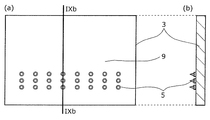
- FIG. 9 is a process diagram showing a method of manufacturing a semiconductor module according to the second embodiment, wherein (a) is a plan view and (b) is a cross-sectional view taken along line IXb-IXb of (a).
- FIG. 10 is a process sectional view showing a method of manufacturing a semiconductor module according to the second embodiment, wherein (a) is a plan view and (b) is a sectional view taken along line Xb-Xb of (a).
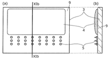
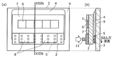
- FIG. 11 is a process sectional view showing a method of manufacturing a semiconductor module according to the second embodiment, wherein (a) is a plan view and (b) is a sectional view taken along line XIb-XIb of (a).
- FIG. 12 is a process sectional view showing a method of manufacturing a semiconductor module according to the second embodiment, wherein (a) is a plan view and (b) is a sectional view taken along line XIIb-XIIb of (a).
- FIG. 13 is a process sectional view showing a method for manufacturing a semiconductor module according to the second embodiment, wherein (a) is a plan view and (b) is a sectional view taken along line XIIIb-XIIIb of (a).
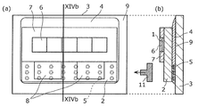
- FIG. 14 is a process sectional view showing a method of manufacturing a semiconductor module according to the second embodiment, wherein (a) is a plan view and (b) is a sectional view taken along line XIVb-XIVb of (a).
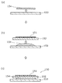
- FIG. 15 is a cross-sectional view showing a method of manufacturing a semiconductor module according to a comparative example.
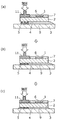
- FIG. 16 is a cross-sectional view showing steps of a method of manufacturing a semiconductor module according to a modification of the second embodiment.
- FIG. 17 is a cross-sectional view showing a first example of a semiconductor module according to the prior art.
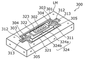
- FIG. 18 is a perspective view showing a second example of the semiconductor module according to the prior art.
- FIG. 17 A first example of a prior art semiconductor module is shown in FIG.
- the LED chip 202 is mounted on the LED package substrate 201.
- the LED package 203 is mounted on the wiring board 204.
- the heat sink 206 Directly below the LED package 203 is bonded to the heat sink 206 with a solder connection or a high thermal conductivity adhesive 205.
- each LED element (semiconductor element) 323 is provided with the positive electrode land 324a and the negative electrode land 324b of the heat dissipation substrate 321 via the submount 322 which is a mounting structure including the mounted wiring substrate. And the submount 322 is mounted on the top surface of the heat dissipation substrate 321.
- the optical center is determined based on the optical position of the semiconductor elements.
- the semiconductor module is mounted on the housing, the reference hole of the heat dissipation substrate is used. Therefore, in the semiconductor module, the requirements for mounting accuracy with respect to the optical center and the reference position of the heat dissipation substrate are severe. As a result, highly accurate alignment is required for bonding the wiring substrate or the submount to the heat dissipation substrate.
- the bonding material (die bonding material) is mounted on the heat dissipation substrate 321, and the temperature is raised and melted. .
- the submount 322 is picked up by a mounting head tool (not shown) and mounted on the bonding material.
- the submount 322 is placed at a predetermined position while being held by the mounting head tool.
- the submount 322 is joined and held with the bonding material, and is allowed to cool and solidify.
- the submount 322 is released without being held by the mounting head tool, the submount 322 is not fixed in position, and it becomes impossible to control the mounting accuracy and the height variation.
- a heat dissipation substrate based on a metal such as Cu generally used has a high heat capacity, takes a very long time to reach a target temperature during temperature rise and cooling, and the process tact of mounting becomes long.
- the holding time of the submount with the mounting head tool is not ensured long, the required accuracy such as the mounting accuracy, height, and tilt required for the optical element etc. can not be satisfied. That is, it is difficult to achieve both shortening the process tact time and maintaining high accuracy.
- FIG. 1 is a schematic view schematically showing a configuration of a semiconductor module 100 according to the present embodiment.
- FIG. 1A is a plan view.
- (B) of FIG. 1 is a cross-sectional view taken along line Ib-Ib of (a).
- FIG. 1C is a cross-sectional view taken along the line Ic-Ic in FIG.
- a semiconductor module 100 shown in (a) of FIG. 1 to (c) of FIG. 1 has a semiconductor element 1 and a wiring board on which the semiconductor element 1 is mounted on its first surface and electrically connected to the semiconductor element 1. 2 and a heat dissipation substrate 3 mounting the wiring substrate 2 on a third surface opposite to the second surface opposite to the first surface of the wiring substrate 2, and a first metal bonding the wiring substrate 2 and the heat dissipation substrate 3
- the system material 4 and the second metal-based material 5 are provided.
- the wiring substrate 2 is a first substrate
- the heat dissipation substrate 3 is a second substrate.
- the long side direction of the wiring board 2 is taken as the X axis direction, the short side direction of the wiring board 2 as the Y axis direction, and the direction orthogonal to the X axis direction and the Y axis direction as the Z axis direction.
- the semiconductor element 1 is, for example, an optical element, and a light emitting element such as an LED or a laser is used.
- the semiconductor element 1 is mounted on the wiring board 2 and electrically connected to the wiring board 2.
- the state in which the semiconductor element 1 is mounted on the wiring substrate 2 may be collectively referred to as a submount.
- the light transmitting member 6 may cover the surface of the semiconductor element 1.
- the light transmitting member 6 is, for example, a phosphor, and light from the semiconductor element 1 is emitted to the outside through the light transmitting member 6.
- the wiring substrate 2 is a substrate on which an electrode used for connection to the semiconductor element 1 and a wiring electrically connected to the semiconductor element 1 are disposed.
- a plating material may be disposed on the surface of the wiring board 2 as a first metal film.
- the plating material constituting the first metal film may be, for example, a material containing Au, such as Ni / Pd / Au plating.
- a plurality of semiconductor elements 1 are mounted on the first surface of the wiring board 2.
- the control substrate other than the semiconductor device 1 may be mounted on the wiring substrate 2. Thus, the manner or brightness of light emission of the semiconductor element 1 may be controlled.
- the wiring board 2 is required to have high heat dissipation.
- the wiring board 2 in order to mount the semiconductor element 1 with high precision and to ensure the reliability of the mounting position of the semiconductor element 1, the wiring board 2 needs to have a linear expansion coefficient relatively close to that of the semiconductor element 1. It is.
- aluminum nitride is used for the wiring substrate 2.
- the wiring substrate 2 is not limited to aluminum nitride, and other ceramic materials, organic substrates formed of resin materials, or the like may be used.
- electrodes 8 for electrically connecting the semiconductor element 1 to the heat dissipation substrate 3, which will be described later, are also formed on the wiring board 2. There is.
- the heat dissipation substrate 3 is a substrate on which the wiring substrate 2 on which the semiconductor element 1 is mounted is mounted and which dissipates the heat of the semiconductor element 1 conducted through the wiring substrate 2.
- the wiring substrate 2 is mounted on the third surface opposite to the second surface opposite to the first surface of the wiring substrate 2.
- the surface of the third surface of the heat dissipation substrate 3 is a die pad region 9 for connection to the second surface of the wiring substrate 2 and an electrode 10 for electrical connection with the electrode 8 on the wiring substrate 2 (see FIG. 8) And are provided.
- the die pad region portion 9 is a bonding pad for bonding the wiring substrate 2, and the second metal film is disposed on the surface of the base material disposed on the third surface of the heat dissipation substrate 3 by plating. It is an area.
- the plating material is, for example, a metal film made of Au.
- the plating material constituting the second metal film is not limited to Au, but may be plating such as NiAu.
- the die pad area portion 9 may be a surface of a Cu base material subjected to Ni / Pd / Au plating treatment.
- a reference hole (not shown), which serves as a mounting reference when mounting on an optical device as the completed semiconductor module 100, is formed in the heat dissipation substrate 3.
- the reference hole is made to match the reference hole on the optical device side, and the semiconductor module 100 is fixed to the device side by screwing.
- a first metal-based material 4 and a second metal-based material 5 are disposed between the heat dissipation substrate 3 and the wiring substrate 2.
- the heat dissipation substrate 3 and the wiring substrate 2 are joined by the first metal-based material 4 and the second metal-based material 5.
- the term "joining" as used herein includes metal bonding and alloying.
- the first metal-based material 4 is a solder material which spreads wet between the wiring substrate 2 and the heat dissipation substrate 3 by melting by heating, and joins the wiring substrate 2 and the heat dissipation substrate 3.
- the first metal-based material 4 is disposed so as to cover the projection surface of the semiconductor element 1 when the semiconductor module 100 is viewed in plan. Further, as shown in FIG. 1C, the first metal-based material 4 is bonded to the second metal-based material 5.
- the first metal-based material 4 a metal-based die-bonding material generally having high heat dissipation and having wettability to the wiring substrate 2 and the heat dissipation substrate 3 is used.
- an AuSn-based solder material is used as the first metal-based material 4.
- a material such as a SnAgCu-based solder material, an Ag nanomaterial, or the like having a high metal filling rate may be used as the first metal-based material 4.
- the first metal material 4 absorbs the difference in thermal expansion between the wiring substrate 2 and the heat dissipation substrate 3 to maintain the reliability of bonding between the wiring substrate 2 and the heat dissipation substrate 3. It is desirable that the coefficient of linear expansion between the heat dissipation substrates 3 be set. For example, when using aluminum nitride as the wiring substrate 2, the linear expansion coefficient of aluminum nitride is 4 to 5 ppm / k, and when using Cu as the heat dissipation substrate 3, the linear expansion coefficient of Cu is 16 to 18 ppm / k. A material having a linear expansion coefficient of 7 to 14 ppm / k may be used as the first metal-based material 4.
- the first metal-based material 4 is disposed at another location of the same die pad region 9 after the second metal-based material 5 is bonded to the die pad region 9 on the heat dissipation substrate 3 as described later.
- the first metal-based material 4 may be disposed at the periphery of the second metal-based material 5.
- the bonding area between the first metal-based material 4 and each of the wiring substrate 2 and the heat dissipation substrate 3 is larger than the bonding area between the second metal-based material 5 and each of the wiring substrate 2 and the heat dissipation substrate 3.
- the first metal-based material 4 may protrude from at least one side of the periphery of the wiring board 2 when the wiring board 2 and the heat dissipation board 3 are viewed in plan.
- the die pad region 9 may be the same die pad region where the first metal material 4 and the second metal material 5 are disposed, or the die pad region where the first metal material 4 is disposed. As a part, a die pad area other than the die pad area where the second metal-based material 5 is disposed may be provided.
- the second metal-based material 5 is a bump which is disposed between the wiring substrate 2 and the heat dissipation substrate 3 and is pressed by the wiring substrate 2 to press-bond the wiring substrate 2 and the heat dissipation substrate 3.
- the second metal-based material 5 is disposed in an area other than the projection plane of the semiconductor element 1 when the semiconductor module 100 is viewed in plan.
- the second metal-based material 5 may be disposed in the heat dissipation substrate 3 in a region other than the region in which the semiconductor element 1 and the reflective resin 7 are disposed.
- the second metal-based material 5 is disposed to fix the wiring substrate 2 and the heat dissipation substrate 3 in a short time to maintain the mounting accuracy in the process of mounting the wiring substrate 2 on the heat dissipation substrate 3. Therefore, the second metal-based material 5 is preferably a material that is more susceptible to plastic deformation than the first metal-based material 4.
- a metal-based bump such as AuSn, Au or the like is used as the second metal-based material 5.
- the first metal-based material 4 and the second metal-based material 5 may be made of different materials or may be made of the same material. When the first metal-based material 4 and the second metal-based material 5 are composed of the same material, the first metal-based material 4 and the second metal-based material 5 are metals. Bonded by bonding.
- the first metal-based material 4 and the second metal-based material 5 are not electrically joined to any of the semiconductor element 1 and the wiring board 2 respectively.
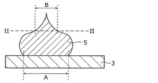
- FIG. 2A is a schematic cross-sectional view showing an example of the shape of the second metal-based material 5 of the semiconductor module 100 according to the present embodiment.
- the second metal-based material 5 shown in FIG. 2A is the second metal-based material 5 bonded to the heat dissipation substrate 3 and before the wiring substrate 2 is bonded.
- the second metal-based material 5 before the wiring substrate 2 is bonded has a shape having a leading end portion which is narrowed so that the cross-sectional area decreases with distance from the heat dissipation substrate 3 .
- the second metal-based material 5 is not limited to the shape illustrated in FIG. 2A as long as the second metal-based material 5 has a tip portion, and may be, for example, a shape in which a cylinder and a cone are combined.
- the front end portion of the second metal-based material 5 is pressed to the load and applied to the wiring substrate 2, for example, is crushed to a position of a II-II line shown in FIG. Be done. Note that, in the second metal-based material 5 after the wiring substrate 2 is bonded, the bonding area B with the wiring substrate 2 is smaller than the bonding area A with the heat dissipation substrate 3.
- the second metal-based material 5 may have a melting point higher than the melting point of the first metal-based material 4 in order to prevent the fixed state from being broken due to remelting at the time of heat bonding of the first metal-based material 4 preferable. Also, when the first metal-based material 4 wets and spreads so as to contact the second metal-based material 5 on the heat dissipation substrate 3, at least the first metal-based material 4 and the second metal-based material 5 It is preferable to use a material that becomes strong by partial bonding.
- the second metal-based material 5 is not limited to Au, and may be another metal.
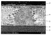
- FIG. 2B is an SEM sectional view showing a bonded portion in which the wiring substrate 2 and the heat dissipation substrate 3 of the semiconductor module 100 according to this embodiment are bonded by the first metal-based material 4 and the second metal-based material 5.
- a solder made of AuSn is used as the first metal-based material 4, and a bump made of Au as the second metal-based material 5.
- the white parts indicate Sn and the gray parts indicate Au.
- the second metal-based material 5 is ultrasonically bonded to the die pad region 9 on the heat dissipation substrate 3 before the wiring substrate 2 is disposed.
- the bonding of the second metal-based material 5 to the heat dissipation substrate 3 may be thermocompression bonding instead of ultrasonic bonding.
- the second metal-based material 5 is bonded to a second metal film (plating material) disposed on the surface of the die pad region 9. At this time, the second metal-based material 5 and the second metal film are metal bonds, or atoms forming the second metal-based material 5 and the second metal film are close to each other or condensed. It is joined.
- the second metal-based material 5 is an Au bump
- the die pad region 9 is a surface of a Cu base material plated with Ni / Pd / Au as a second metal film.
- the Au of the second metal-based material 5 and the Au contained in the second metal film are integrated by ultrasonic bonding, so the second metal-based material 5 and the second metal of the die pad region portion 9 are integrated. The bonding interface with the membrane will not be seen.
- the second metal-based material 5 is bonded to the die pad region 9 of the heat dissipation substrate 3, and the first metal-based material 4 before heating is placed on the die pad region 9. Then, it is thermocompression-bonded to the upper part of the second metal-based material 5. That is, the second metal-based material 5 is plastically deformed when the wiring substrate 2 is abutted and pressurized, and is joined to the wiring substrate 2 (specifically, the first metal film on the surface of the wiring substrate 2) Be done. Thus, the wiring substrate 2 is fixed to the heat dissipation substrate 3 via the second metal-based material 5.
- the wiring board 2 is pressure-bonded (or thermocompression-bonded) in a short time so as to plastically deform the Au bumps of the second metal-based material 5, the wiring board 2 is formed with the first metal film on the surface of the wiring board 2 It is not integrated with the second metal-based material 5, and a clear bonding interface exists.
- the first metal-based material 4 is a temperature higher than the melting point of the first metal-based material 4 and the second after the plastic deformation of the second metal-based material 5 or while plastically deforming the second metal-based material 5. Since it is heated at a temperature equal to or lower than the melting point of the metal-based material 5, it is thermally melted and joined to the wiring substrate 2 and the heat dissipation substrate 3 while wetting and spreading along the height of the second metal-based material 5 after plastic deformation. . At this time, in the same die pad region 9 on the heat dissipation substrate 3, as shown in FIG. 2B, the first metal-based material 4 and the second metal-based material 5 respectively melt and at least a part of each other It is in an alloyed state.
- the second metal-based material 5 is a eutectic portion of the first metal-based material 4
- the metal component of the particle size between the particle size of the first metal-based material 4 and the particle size of the second metal-based material 5 is clearly observed. That is, it can be seen that the first metal-based material 4 and the second metal-based material 5 are integrated and joined.
- first metal-based material 4 and the second metal-based material 5 cause solid phase diffusion to each other, Alternatively, they are joined by forming an alloy.
- the wiring board 2 and the first metal-based material 4, and the heat dissipation board 3 and the first metal-based material 4 are also melted and at least a part of each other is intruded into each other to be alloyed.
- surface plating of the wiring substrate 2 and a die pad region of the heat dissipation substrate 3 Since Au of the surface plating of 9 is diffused into the first metal-based material 4 by high temperature, the surface plating of the wiring substrate 2 and the first metal-based material 4 and the surface of the die pad region 9 of the heat dissipation substrate 3
- the plating and the first metal-based material 4 are integrated, and no bonding interface can be seen.
- the wiring board 2, the heat dissipation board 3, the first metal-based material 4 and the second metal-based material 5 are integrated and joined together, so the wiring board 2, the heat dissipation board 3, the first metal
- the overall bonding strength of the base material 4 and the second metal base material 5 can be improved. Further, even when the second metal-based material 5 is small, the bonding strength and bonding of the wiring substrate 2 and the heat dissipation substrate 3 can be achieved by integrating the first metal-based material 4 and the second metal-based material 5. Reliability can be improved.
- the height of the first metal-based material 4 and the second metal-based material 5 after bonding the wiring substrate 2 and the heat dissipation substrate 3 is between 20 and 70 ⁇ m from the balance of reliability and heat dissipation. It is desirable to be set.
- the height variation including the two materials of the first metal-based material 4 and the second metal-based material 5 is very small in the actual finished state, and is about ⁇ 20 ⁇ m. be able to.
- the 1st metal-based material 4 will become easy to maintain height after melting. Further, since the first metal-based material 4 is disposed in a large area directly below the semiconductor element 1, heat dissipation to the heat dissipation substrate 3 can be efficiently promoted.
- the electrical connection between the heat dissipation substrate 3 and the wiring substrate 2 is not the first metal-based material 4 but, as will be described later, with metal wires such as aluminum, Au or Cu separately on the wiring substrate 2
- the electrodes 8 and the electrodes 10 on the heat dissipation substrate 3 may be directly bonded and bonded.
- connector parts, thermistors, and chips are disposed on the heat dissipation substrate 3.
- a component etc. may be mounted and general solder mounting may be performed by heating, such as reflow, and the semiconductor module 100 may be produced.
- the second metal having a high melting point when bonding the wiring substrate 2 and the heat dissipation substrate 3 with the first metal material 4 and the second metal material 5. While maintaining the state in which the wiring substrate 2 and the heat dissipation substrate 3 are fixed by the base material 5, the first metal-based material 4 is melted and brought into contact with the second metal-based material 5.
- the heat dissipation substrate 3 can be joined in a short time.
- the process tact can be shortened.
- the mounting head tool 11 is a tool that holds the wiring board 2 on which the semiconductor element 1 is mounted by suction.
- the mounting head tool 11 can contact and pressurize the second metal-based material 5 while adsorbing the wiring board 2.
- the mounting head tool 11 is not limited to a tool for holding the wiring substrate 2 by suction, and may hold the wiring substrate 2 by another method such as holding the wiring substrate 2 or the like.
- LED element 1 the light emitting diode used as the semiconductor element 1 is referred to as the LED element 1.
- a plurality of LED elements 1 are arranged in a line along the long side direction of the wiring substrate 2.
- Each LED element 1 is flip-chip connected to an electrode (not shown) on the wiring board 2.
- a light transmitting member 6 is disposed above the individual LED elements 1 via an adhesive (not shown).
- a reflective resin 7 is disposed in the area around the LED element 1 and the light transmitting member 6 on the wiring substrate 2.
- the reflecting resin 7 covers the side surface of the LED element 1 and the side surface of the light transmitting member 6 to expose the surface of the light transmitting member 6.
- the end of the reflective resin 7 coincides with the positions of the three sides of the wiring board 2.
- the lower half of the upper surface of the wiring board 2 is exposed from the reflective resin 7 in FIG. In other words, a part of the electrode electrically connected to the LED element 1 on the wiring substrate 2 is exposed so as to extend from the reflective resin 7.
- the light transmitting member 6 is a ceramic plate containing a phosphor for converting the wavelength of the light emitted from the LED element 1.
- White light is obtained by the blue light emitted from the LED element 1 and the converted light wavelength-converted by the phosphor being emitted from the emission surface of the light transmitting member 6.
- the phosphor is, for example, a known material such as YAG, CASN, SiAlON, LSN or the like.
- the reflective resin 7 is, for example, a silicone resin containing a reflective material such as titanium oxide.
- the wiring substrate 2 is fixed to the die pad region 9 on the heat dissipation substrate 3.
- a first metal film (not shown) composed of NiCr / Au / Ni / Au is provided in order from the side close to the wiring substrate 2 on the surface facing the heat dissipation substrate 3 of the wiring substrate 2.
- a second metal film (not shown) composed of Ni / Pd / Au is provided on the die pad region 9 on the heat dissipation substrate 3 in order from the side close to the heat dissipation substrate 3.
- Wiring substrate 2 and heat dissipation substrate 3 are formed of a second metal-based material 5 made of Au and disposed between the first metal film and the second metal film of each of wiring substrate 2 and heat dissipation substrate 3.
- the first metal-based material 4 made of AuSn.
- the second metal-based material 5 is provided only under the region other than the region where the LED element 1 and the reflective resin 7 are disposed on the wiring substrate 2 when the semiconductor module 100 is viewed from the top.
- the plurality of second metal-based materials 5 are arranged in a matrix of 3 rows and 8 columns on the wiring substrate 2.
- the first metal-based material 4 is disposed on the entire lower surface of the area where the LED element 1 and the reflective resin 7 are formed when the semiconductor module 100 is viewed from above, and a plurality of the first metallic materials 4 are further disposed in a matrix. It is also arranged to fill the space between the second metal-based materials 5. That is, the first metal-based material 4 is formed on the entire lower region of the wiring substrate 2. Therefore, only the first metal-based material 4 is disposed between the wiring substrate 2 and the heat dissipation substrate 3 immediately below the LED element 1.
- the side walls of the second metal-based material 5 composed of Au are in contact with the first metal-based material 4 composed of AuSn. Furthermore, in the process of spreading the first metal-based material 4 so as to fill the spaces between the plurality of second metal-based materials 5, the side wall of the second metal-based material 5 and the first metal-based material 4 melt Joint. In other words, the columnar second metal-based material 5 is formed so as to penetrate the inside of the first metal-based material 4 formed on the entire surface of the die pad region portion 9.
- the second metal-based material 5 is integrated with Au on the outermost surface of the metal film of the heat dissipation substrate 3 by ultrasonic bonding, so that a metal bond is formed partially or in the entire area, and the interface Is not clear. Further, since the second metal-based material 5 is thermocompression-bonded to Au on the outermost surface of the metal film of the wiring substrate 2, no metal bonding is formed, and a clear interface is observed.
- the LED element 1 of high brightness has a large amount of heat generation
- the arrangement area of the LED element 1 and the wide side on the back side of the area around the LED element 1 where the reflection resin 7 is arranged Since the wiring substrate 2 and the heat dissipation substrate 3 are directly fixed by the first metal-based material 4 in the region, the heat generated in the LED element 1 can be rapidly dissipated to the heat dissipation substrate 3 side.
- the second metal material 5 is disposed on the back side of the area where the reflective resin 7 is not formed, so that the mounting head tool 11 directly presses the upper surface of the wiring board 2. it can.
- the wiring substrate 2 and the heat dissipation substrate 3 can be fixed by the second metal-based material 5 without applying pressure to the reflective resin 7 having a smaller Young's modulus than the wiring substrate 2.
- the second metal-based material 5 is arranged in a matrix of 3 rows and 8 columns, but at least three second metal-based materials 5 may be arranged.
- three second metal-based materials 5 are used. You may arrange so that a surface may be formed. Also, depending on the machine accuracy of the mounting head tool 11, three may be disposed on a straight line.
- the second melting point is high when the wiring substrate 2 and the heat dissipation substrate 3 are joined by the first metal-based material 4 and the second metal-based material 5.
- the first metal-based material 4 is melted while being in contact with the second metal-based material 5 while maintaining the state in which the wiring substrate 2 and the heat dissipation substrate 3 are fixed by the metal-based material 5 of 2 and the heat dissipation substrate 3 are joined in a short time.
- the displacement due to the mounting deviation between the wiring substrate 2 and the heat dissipation substrate 3 or the difference in the linear expansion coefficient of the material is suppressed. it can.
- the fixed state can be more firmly maintained even after the joining.
- the process tact can be shortened. Therefore, a highly reliable semiconductor module 100 can be obtained in a short time.
- the heat generated in the semiconductor element 1 can be efficiently dissipated through the heat dissipation substrate 3.
- the first metal-based material 4 is joined to the die pad region 9 of the heat dissipation substrate 3 by melting the first metal-based material 4, so the area is larger than that of the second metal-based material 5. It is.
- the first metal-based material 4 has a bonding area larger than that of the second metal-based material 5, and the second metal in a projection plane when viewed in plan from the semiconductor element 1 side.
- the arrangement region of the base material 5 is unevenly distributed on one side of the wiring board 2 excluding the region directly below the semiconductor element 1, and the arrangement region of the first metal base material 4 substantially covers the entire surface directly below the wiring substrate 2. Arranged and joined.
- the semiconductor element 1 is shifted from the center of the wiring board 2, and only the first metal-based material 4 is disposed below the wiring board 2 directly below the semiconductor element 1.
- the second metal-based material 5 is disposed immediately below the wiring substrate 2 on which the semiconductor element 1 is not mounted. That is, the second metal-based material 5 is located between the region in which the semiconductor element 1 is disposed and one side of the wiring substrate 2 when the heat dissipation substrate 3 in which the second metal-based material 5 is disposed is viewed in plan. It is arranged.
- semiconductor modules 100b to 100d according to a to c of the first modification of the first embodiment will be described.
- the LED element 1 is used as the semiconductor element 1.
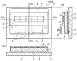
- FIG. 3 is a schematic view showing a configuration of a semiconductor module 100b according to a of a first modified example of the present embodiment.
- (a) is a plan view
- (b) is a cross-sectional view taken along line IIIb-IIIb in (a)
- (c) is a cross-sectional view taken along line IIIc-IIIc in (a).
- the semiconductor module 100b of the first modification example shown in (a) to (c) of FIG. 3 is disposed on the wiring board 2 in comparison with the semiconductor module 100 shown in (a) to (c) of FIG.
- the LED element 1, the light transmitting member 6, and the reflecting resin 7 have the same configuration, and the number and arrangement of the second metal-based materials 5 are different. Specifically, when the semiconductor module 100b is viewed from the top as shown in FIG.
- the second metal-based material 5 is provided in two places near the reflective resin 7 and near both ends of the wiring substrate 2 and a region where the reflective resin 7 is disposed. They are disposed at a total of three places, one near the center of the end of the wiring board 2 remote from the other.
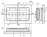
- FIG. 4 is a cross-sectional view showing a configuration of a semiconductor module 100c according to b of the first modified example of the present embodiment.
- (a) is a plan view
- (b) is a cross-sectional view taken along line IVb-IVb in (a)
- (c) is a cross-sectional view taken along line IVc-IVc in (a).
- the semiconductor module 100c of b of the first modification shown in (a) to (c) of FIG. 4 is disposed on the wiring board 2 in comparison with the semiconductor module 100b shown in (a) to (c) of FIG.
- the arrangement of the LED element 1, the light transmitting member 6, the reflecting resin 7 and the second metal-based material 5 is different. Specifically, when the semiconductor module 100c is viewed from the top as shown in FIG. 4A, the LED element 1 and the reflecting resin 7 are disposed to cross the center of the wiring board 2 and both sides thereof The electrodes 8 of the wiring board 2 are exposed.
- the second metal-based material 5 is a reflective resin in the region of the wiring substrate 2 where the LED element 1 and the reflective resin 7 are disposed, and in the region excluding the lower side of the region where the electrodes 8 of the wiring substrate 2 are disposed. 7 are disposed at a total of three places: one place near the center of one end of the wiring board 2 and two places near both corners of the other end.
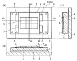
- FIG. 5 is a cross-sectional view showing a configuration of a semiconductor module 100d according to c of the first modified example of the present embodiment.
- (a) is a plan view
- (b) is a cross-sectional view taken along the line Vb-Vb of (a)
- (c) is a cross-sectional view taken along the line Vc-Vc of (a).
- the semiconductor module 100d of the first modification c shown in (a) to (c) of FIG. 5 is disposed on the wiring board 2 in comparison with the semiconductor module 100b shown in (a) to (c) of FIG.
- the arrangement of the electrode, the LED element 1, the light transmitting member 6, the reflecting resin 7, and the second metal-based material 5 is different. Specifically, when the semiconductor module 100d is viewed from the top as shown in FIG. 5A, the LED elements 1 are arranged in a 2 ⁇ 3 matrix along the long side direction of the wiring board 2 It is done.
- the reflecting resin 7 covers the side surfaces of the LED element 1 and the light transmitting member 6, and is disposed to cross the short side direction of the wiring board 2.
- the electrodes 8 of the wiring board 2 are exposed from the reflecting resin 7 so as to extend in the long side direction of the wiring board 2.
- the second metal-based material 5 is a wiring in a region on the wiring substrate 2 where the LED element 1 and the reflective resin 7 are disposed, and in a region excluding the region below the region where the electrodes 8 of the wiring substrate 2 are disposed. In the vicinity of the four corner portions of the substrate 2, they are arranged at a total of four places of one place.
- the second metal-based materials 5 are arranged in a matrix, but in the semiconductor modules 100b to 100d according to a to c of this modification, the electrodes on the wiring board 2
- the second metal-based material 5 is disposed below the same thickness portion avoiding 8.
- the plurality of second metal-based materials 5 are dispersed and disposed, whereby the mounting head tool 11 is used.
- the second metal-based material 5 may be arranged such that a line connecting the second metal-based material 5 forms a surface at at least three locations. Further, the second metal-based material 5 may be disposed at three places on a straight line depending on the mechanical accuracy of the mounting head tool 11.
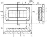
- FIG. 6 is a schematic view showing the configuration of a semiconductor module according to a second modification of the first embodiment. 6, (a) is a plan view, (b) is a cross-sectional view taken along the line VIb-VIb of (a), and (c) is a cross-sectional view taken along the line VIc-VIc of (a).
- the semiconductor module 100 e shown in (a) to (c) of FIG. 6 has an LED element 1 disposed on the wiring substrate 2 in comparison with the semiconductor module 100 shown in (a) to (c) of FIG.
- the arrangement of the transmitting member 6, the reflecting resin 7, and the second metal-based material 5 is different. Specifically, when the semiconductor module 100e is viewed from the top as shown in FIG. 6A, the LED elements 1 are arranged in two rows and five columns along the long side direction (X axis direction) of the wiring board 2 It is arranged.
- the reflecting resin 7 covers the side surfaces of the LED element 1 and the light transmitting member 6 and is disposed on the entire surface of the wiring substrate 2 except for the four corner portions of the wiring substrate 2.
- the second metal-based material 5 is disposed at all four corners of the wiring substrate 2 in the region excluding the lower side of the region on the wiring substrate 2 where the LED element 1 and the reflective resin 7 are disposed.
- the wiring board 2 is flat by pressing the four corner portions of the wiring board 2 on which the second metal-based material 5 is disposed downward with the mounting head tool 11 since the wiring board 2 is flat.
- the degree of parallelism can be maintained when fixed to Therefore, in the semiconductor module 100e, good mounting stability of the wiring substrate 2 and the heat dissipation substrate 3 can be obtained.
- FIG. 7 is a schematic view showing the configuration of a semiconductor module 100f according to a third modification of the first embodiment.
- (a) is a plan view
- (b) is a cross-sectional view taken along line VIIb-VIIb in (a)
- (c) is a cross-sectional view taken along line VIIc-VIIc in (a).
- a semiconductor module 100f shown in (a) to (c) of FIG. 7 has an LED element 1 disposed on the wiring substrate 2 in comparison with the semiconductor module 100e shown in (a) to (c) of FIG.
- the arrangement of the transmitting member 6, the reflecting resin 7, and the second metal-based material 5 is different.
- the semiconductor module 100 f is viewed from the top as shown in FIG. 7A, the three LED elements 1 are arranged in one row along the long side direction (X-axis direction) of the wiring board 2.
- the reflecting resin 7 is disposed so as to cover the side surfaces of the LED element 1 and the light transmitting member 6 and not to be in contact with the end of the wiring substrate 2.
- the second metal-based material 5 is an area excluding the lower side of the area on the wiring board 2 where the LED element 1 and the reflective resin 7 are arranged, and the lower side of the area where the electrode 8 of the wiring board 2 is arranged. In the area
- the semiconductor module 100 f has the largest area of the area exposed from the LED element 1 and the reflective resin 7 of the wiring board 2 compared to the semiconductor module 100 e according to the second modification. Pressure can be applied by the mounting head tool 11 along the four sides of the outer peripheral portion. Therefore, in the semiconductor module 100 f, the mounting inclination when fixing the wiring board 2 to the heat dissipation board 3 can be minimized, and further better mounting stability of the wiring board 2 and the heat dissipation board 3 can be obtained.
- FIG. 8 is a cross-sectional view showing the configuration of a semiconductor module 100g according to a fourth modification of the present embodiment.
- the feature of the semiconductor module 100g according to the present modification is that, as shown in FIG. 8, the electrode 8 on the wiring substrate 2 on which the semiconductor element 1 is mounted and the electrode 10 on the heat dissipation substrate 3 are Cu, Au, etc. , Al, etc., and the first metal-based material 4 is not electrically conducted to any of the semiconductor element 1 and the wiring board 2.
- the semiconductor module 100 g can electrically connect the semiconductor element 1 and the wiring board 2 to the heat dissipation board 3. Connections are made between the respective electrodes 8 and 10. Thereby, the semiconductor module 100 f maintains the electrical characteristics to function as a semiconductor module regardless of the bonding state of the wiring substrate 2 and the heat dissipation substrate 3 by the second metal-based material 5 and the first metal-based material 4. be able to.
- the second metal-based material 5 it is desirable to select a material having a thermal conductivity higher than that of the first metal-based material 4 and place the material immediately below the electrode 8 of the wiring substrate 2. In this manner, after the wiring substrate 2 is mounted on the heat dissipation substrate 3, the wiring substrate 2 can be electrically connected with the electrodes 8 on the wiring substrate 2 by the metal wires 12 and the electrodes 10 on the heat dissipation substrate 3.
- the second metal-based material 5 is disposed immediately below the electrode 8 of FIG. Therefore, the heat conduction between the heat dissipation substrate 3 and the wiring substrate 2 immediately below the electrode 8 is improved.
- the electrode 8 and the electrode 10 are bonded by the metal wire 12 and heating is required from the side of the heat dissipation substrate 3, the electrode 8 can be favorably heated. Therefore, the wiring substrate 2 and the heat dissipation substrate 3 can be stably joined by the metal wires 12.
- the first metal-based material 4 has a melting point lower than that of the second metal-based material 5. Further, the bonding area of the first metal-based material 4 is larger than that of the second metal-based material 5. Furthermore, compared to the first metal-based material, the second metal-based material 5 is easily deformed by a load at the time of bonding, and hardly spreads wet.
- the second metal-based material 5 be a bump made of a metal having a Young's modulus of 150 GPa or less
- the first metal-based material 4 be a solder.
- Au bump and AuSn solder (Cu, Ag, Au) bump and SnAg solder, (Cu, Ag, Au) bump and SnPb solder, Sn bump and SnAg solder or SnPb solder, Bi bump and SnAg solder
- a combination of solder, SnBi solder, Pb bump and SnPb solder, In bump and SnAg solder, SnPb solder, Al bump and SnZn solder is desirable.
- the second metal-based material 5 can be mounted on the heat dissipation substrate 3 and joined, and then the first metal The system material 4 can be mounted on the heat dissipation substrate 3. At that time, the stage under the heat dissipation substrate 3 can be heated so that the temperature of the first metal-based material 4 becomes equal to or higher than the melting point. Next, the wiring substrate 2 is held by the mounting head tool 11, and the first metal substrate 5 is pressed against the second metal material 5 so as to plastically deform the second metal material 5. The first metal-based material 4 is brought into contact with the second metal-based material 5 by bringing the metal-based material 4 into contact and further pressing the wiring substrate 2. Can be spread out.
- first metal-based material 4 and the second metal-based material 5 with the same metal such as Au-based, Cu-based, Ag-based, Sn-based, Bi-based, Pb-based and In-based, Facilitating suppression of void formation in the first metal-based material 4 and the second metal-based material 5 at the time of joining the first metal-based material 4 and the second metal-based material 5 Can.
- FIGS. 9 to 14 are process sectional views showing a method of manufacturing the semiconductor module 100.
- (a) is a plan view
- (b) is an IXb-IXb line, an Xb-Xb line, an XIb-XIb line, a XIIb-XIIb line, and an XIIIb line shown in (a) of each figure.
- 7 is a cross-sectional view taken along the line XIIIb and the line XIVb-XIVb.
- the second metal-based material 5 is mounted on a predetermined region of the die pad region 9 on the heat dissipation substrate 3 (second metal-based material mounting step).
- a metal bump such as Au or Cu is used as the second metal-based material 5
- a stud bump is formed by ultrasonic bonding on the heat dissipation substrate 3.
- the heat dissipation substrate 3 is heated on a heating stage (not shown). Thereafter, the first metal-based material 4 is mounted on the die pad region 9 (a first metal-based material mounting step).
- the first metal-based material 4 is mounted in the form of metal pellets and is heated below the melting point. For example, when using AuSn pellet as a metal pellet, it heats at about 250 degreeC which is the temperature below melting
- the thickness of the metal pellet, which is the first metal-based material 4, is about 50 ⁇ m, and is approximately equal to or slightly smaller than the height of the second metal-based material 5.
- the form of the first metal-based material 4 is not limited to the pellet material, and may be a paste material. However, the amount of shrinkage after heating and cooling is smaller for the pellet material, which is suitable for the present manufacturing method.
- first metal-based material mounting step and the second metal-based material mounting step the order of the steps may be reversed, or the steps may be performed simultaneously.
- first metal-based material mounting step and the second metal-based material mounting step the first metal-based material 4 and the second metal-based material 5 are preferably arranged not to be in contact with each other.
- the heat dissipation substrate 3 is heated to the melting point or more of the first metal-based material 4 (heating step).
- the temperature of the stage (not shown) of the facility supporting the heat dissipation substrate 3 therebelow is set to a temperature such that the temperature of the first metal-based material 4 becomes equal to or higher than the melting point.
- the first metal-based material 4 is melted, but does not spread so much on the heat dissipation substrate 3 or the die pad region 9 and remains at the mounting point at the time of FIG.
- the heat dissipating substrate 3 is placed on the above-described heating stage and kept heated, and the wiring substrate 2 on which the semiconductor element 1 is mounted using the mounting head tool 11 is a first metal-based material 4 and a second metal-based material 4
- the metal based material 5 is prepared above the joined heat dissipating substrate 3 and adjusted to the desired mounting position.
- the wiring board 2 is pressed by the mounting head tool 11 so as to be in contact with the heat dissipation board 3 on which the first metal material 4 and the second metal material 5 are disposed. Pressurization process).
- the wiring board 2 is bonded to the first metal-based material 4 and the second metal-based material 5.
- the wiring board 2 is fixed at a desired position while pressing the wiring board 2 against the tip of the second metal-based material 5 to cause plastic deformation.
- the wiring board 2 is pressed against the first metal-based material 4 in the molten state and extruded in the outer peripheral direction of the heat dissipation board 3 until the desired height is followed.
- the metal-based material 5 of the above may be deformed.
- the first metal-based material 4 wets and spreads between the wiring substrate 2 and the heat dissipation substrate 3 and is at least in contact with or bonded to the second metal-based material 5.
- the first metal-based material 4 and the second metal-based material 5 are melted and joined to the wiring substrate 2 and the heat dissipation substrate 3.
- the loading head tool 11 may be brought into contact with the semiconductor element 1 of the wiring substrate 2 to apply a load, as described in the present embodiment, the semiconductor is disposed above the second metal-based material 5.
- the second metal-based material 5 may be plastically deformed while the element 1 is not mounted and the mounting head tool 11 directly presses the portion of the wiring board 2 on which the semiconductor element 1 is not mounted.
- the first metal-based material 4 and the second metal-based material 5 are disposed on the same bonding pad or the same electrode on the wiring substrate 2, the first metal-based material The material 4 easily wets and spreads until it contacts the second metal-based material 5. Furthermore, the same effect can be obtained if the die pad region portion 9 to which the first metal-based material 4 and the second metal-based material 5 are bonded is the same on the heat dissipation substrate 3 as well.
- the suction between the mounting head tool 11 and the wiring board 2 is released. Even when the adsorption of the mounting head tool 11 and the wiring substrate 2 is released in a state where the AuSn solder of the first metal material 4 is melted, the Au bumps of the second metal material 5 fix the wiring substrate 2 Because of this, positional deviation in the X-axis direction, the Y-axis direction and the Z-axis direction does not occur. Thereafter, the heat dissipation substrate 3 on which the wiring substrate 2 is disposed is removed from the heating stage and cooled, whereby the bonding of the wiring substrate 2 and the heat dissipation substrate 3 is completed.
- the wiring substrate 2 and the heat dissipation substrate 3 are fixed by the second metal-based material 5 when the wiring substrate 2 and the heat dissipation substrate 3 are bonded. Therefore, even if the suction of the mounting head tool 11 and the wiring substrate 2 is released in a state where the first metal-based material 4 is melted, no positional deviation between the wiring substrate 2 and the heat dissipation substrate 3 occurs. As a result, according to the method of manufacturing the semiconductor module 100 according to the present embodiment, the wiring substrate 2 and the heat dissipation substrate 3 can be joined in a short time, and the process throughput can be improved.
- the first metal-based material 4 joins the wiring substrate 2 and the heat dissipation substrate 3 in a large area, and also bonds with the second metal-based material 5. Both of these can provide the semiconductor module 100 having high bonding strength and high reliability.
- FIG. 15 are cross-sectional views showing a method of manufacturing the semiconductor module 150 according to the comparative example.
- the bonding material 154 is disposed on the heat dissipation substrate 153 as shown in FIG. Subsequently, as shown in FIG. 15B, after the bonding material 154 is melted, the wiring substrate 152 on which the semiconductor element 151 is mounted is bonded using the mounting head tool (not shown). Are disposed above the heat dissipation substrate 153 attached. Thereafter, the wiring substrate 152 on which the semiconductor element 151 is mounted is pressed and bonded so as to be in contact with the heat dissipation substrate 153 on which the bonding material 154 is mounted. Furthermore, as shown in (c) of FIG. 15, the semiconductor module 150 is completed by cooling the bonding material 154.
- the wiring substrate 152 on which the semiconductor element 151 is mounted is disposed above the heat dissipation substrate 153 on which the bonding material 154 is mounted, and then the wiring substrate 152 on which the semiconductor element 151 is mounted is It is pressed and joined so as to be in contact with the heat dissipation substrate 153 attached.
- the second metal-based material 5 since the second metal-based material 5 is used, the second metal-based material 5 and the wiring substrate 2 are bonded in the heating process.
- the wiring substrate 2 is fixed to the heat dissipation substrate 3 in accordance with the height of the metal-based material 5. By this fixing, it is possible to control with high accuracy the mounting accuracy of the wiring substrate 2 and the semiconductor element 1 mounted thereon such as height variations and inclinations to the heat dissipation substrate 3.
- the first metal-based material 4 dissipates heat with the wiring substrate 2 in a state where the wiring substrate 2 is fixed to the heat dissipation substrate 3 with the second metal-based material 5
- the substrate 3 is wetted and spreads, and the wiring substrate 2 and the heat dissipation substrate 3 are joined. Therefore, the fixing by the second metal-based material 5 eliminates the need to keep holding the wiring substrate 2 by the mounting head tool 11.
- bonding of the wiring substrate 2 and the heat dissipation substrate 3 by the first metal-based material 4 can be performed in a short time, and the process capacity can be improved.
- FIGS. 16A to 16C are cross-sectional views showing steps of a method of manufacturing a semiconductor module according to a modification of the second embodiment.
- the method of manufacturing the semiconductor module 100 according to the present embodiment is similar to the method of manufacturing the second embodiment shown in FIGS. 9 to 14, so only the difference between the two will be described.
- the first metal as a finished product is changed by changing the pressure condition of the wiring board 2 by the mounting head tool 11.
- the bonding state between the base material 4 and the second metal base material 5 can be changed.
- the first metal-based material 4 is removed by lowering the wiring board 2 to crush the tip of the second metal-based material 5.
- the desired first metal-based material 4 and second metal-based material 5 are joined by bringing them into contact with the metal-based material 5 and wet-spreading immediately below the portion pressed by the mounting head tool 11. There is.
- 16A has an advantage that the bonding state of the second metal-based material 5 with the wiring board 2 and the heat dissipation board 3 can be easily observed by X-ray inspection or the like.
- the wiring board 2 when the wiring board 2 is further pressurized by the mounting head tool 11, the distance between the wiring board 2 and the heat dissipation board 3 is reduced, and the end of the wiring board 2 on the heat dissipation board 3 A fillet in which the first metal-based material 4 is exposed in the outer peripheral direction of the heat dissipation substrate 3 rather than the portion can be formed.
- the bonding strength between the two can be improved.
- the first metal-based material 4 be exposed from the end portions of all the four sides of the wiring board 2 including portions other than the peripheral portion of the second metal-based material 5 to form a fillet.
- the present disclosure is particularly useful in a headlamp using an LED, a semiconductor module mounted with an LED used for a light fixture with high optical accuracy, and the like.
Landscapes
- Cooling Or The Like Of Semiconductors Or Solid State Devices (AREA)
- Led Device Packages (AREA)
Abstract
La présente invention comprend : un élément semi-conducteur (1) ; une carte de base de câblage (2) sur laquelle est installé l'élément semi-conducteur (1) ; une plaque de base de rayonnement thermique (3) ; un premier matériau métallique (4) reliant la carte de base de câblage (2) à la plaque de base de rayonnement thermique (3) ; et un second matériau métallique (5) ayant un point de fusion différent de celui du premier matériau métallique (4) et reliant la carte de base de câblage (2) à la plaque de base de rayonnement thermique (3). Le premier matériau métallique (4) et la carte de base de câblage (2), le premier matériau métallique (4) et la plaque de base de rayonnement thermique (3), le second matériau métallique (5) et la carte de base de câblage (2), le second matériau métallique (5) et la plaque de base de rayonnement thermique (3), et le premier matériau métallique (4) et le second matériau métallique (5) sont reliés au moins partiellement entre eux. Le premier matériau métallique (4) et la carte de base de câblage (2), le premier matériau métallique (4) et la plaque de base de rayonnement thermique (3), et le premier matériau métallique (4) et le second matériau métallique (5) sont alliés, respectivement.
Priority Applications (2)
| Application Number | Priority Date | Filing Date | Title |
|---|---|---|---|
| JP2018562688A JP7201439B2 (ja) | 2017-11-15 | 2018-08-20 | 半導体モジュールおよびその製造方法 |
| US16/285,850 US10847702B2 (en) | 2017-11-15 | 2019-02-26 | Semiconductor module |
Applications Claiming Priority (2)
| Application Number | Priority Date | Filing Date | Title |
|---|---|---|---|
| JP2017-220115 | 2017-11-15 | ||
| JP2017220115 | 2017-11-15 |
Related Child Applications (1)
| Application Number | Title | Priority Date | Filing Date |
|---|---|---|---|
| US16/285,850 Continuation US10847702B2 (en) | 2017-11-15 | 2019-02-26 | Semiconductor module |
Publications (1)
| Publication Number | Publication Date |
|---|---|
| WO2019097790A1 true WO2019097790A1 (fr) | 2019-05-23 |
Family
ID=66537822
Family Applications (1)
| Application Number | Title | Priority Date | Filing Date |
|---|---|---|---|
| PCT/JP2018/030684 Ceased WO2019097790A1 (fr) | 2017-11-15 | 2018-08-20 | Module à semi-conducteur et son procédé de production |
Country Status (3)
| Country | Link |
|---|---|
| US (1) | US10847702B2 (fr) |
| JP (1) | JP7201439B2 (fr) |
| WO (1) | WO2019097790A1 (fr) |
Cited By (1)
| Publication number | Priority date | Publication date | Assignee | Title |
|---|---|---|---|---|
| JP2020107874A (ja) * | 2018-12-25 | 2020-07-09 | 日亜化学工業株式会社 | 光源装置の製造方法および光源装置 |
Families Citing this family (1)
| Publication number | Priority date | Publication date | Assignee | Title |
|---|---|---|---|---|
| EP3675190B1 (fr) * | 2018-12-25 | 2023-05-03 | Nichia Corporation | Procédé de fabrication d'un dispositif de source lumineuse et dispositif de source lumineuse |
Citations (8)
| Publication number | Priority date | Publication date | Assignee | Title |
|---|---|---|---|---|
| US4389557A (en) * | 1981-08-17 | 1983-06-21 | Northern Telecom Limited | Semiconductor laser bonding technique |
| JPH10189801A (ja) * | 1996-12-26 | 1998-07-21 | Matsushita Electric Ind Co Ltd | 半導体装置 |
| JP2010109321A (ja) * | 2008-09-30 | 2010-05-13 | Toyoda Gosei Co Ltd | 発光装置及びその製造方法 |
| JP2015185611A (ja) * | 2014-03-20 | 2015-10-22 | 東芝ライテック株式会社 | 発光装置 |
| WO2016147252A1 (fr) * | 2015-03-13 | 2016-09-22 | 株式会社日立製作所 | Appareil à semi-conducteur et son procédé de fabrication |
| JP2016177979A (ja) * | 2015-03-20 | 2016-10-06 | ウシオ電機株式会社 | 蛍光光源装置 |
| JP2017069401A (ja) * | 2015-09-30 | 2017-04-06 | 日亜化学工業株式会社 | 基板及び発光装置、並びに発光装置の製造方法 |
| WO2017163593A1 (fr) * | 2016-03-24 | 2017-09-28 | パナソニックIpマネジメント株式会社 | Module semi-conducteur et son procédé de fabrication |
Family Cites Families (7)
| Publication number | Priority date | Publication date | Assignee | Title |
|---|---|---|---|---|
| JP2001230351A (ja) * | 2000-02-14 | 2001-08-24 | Shibafu Engineering Corp | 電子モジュール用接合材料、モジュール型半導体装置及びその製造方法 |
| JP2007243118A (ja) * | 2006-03-13 | 2007-09-20 | Fuji Electric Holdings Co Ltd | 半導体装置 |
| WO2009157160A1 (fr) * | 2008-06-25 | 2009-12-30 | パナソニック株式会社 | Structure de conditionnement et procédé de fabrication de structure de conditionnement |
| JP5656247B2 (ja) | 2010-10-05 | 2015-01-21 | シチズン電子株式会社 | 半導体発光装置及び半導体発光装置の組み込み構造 |
| JP4910220B1 (ja) | 2010-10-19 | 2012-04-04 | 国立大学法人九州工業大学 | Ledモジュール装置及びその製造方法 |
| JP5931410B2 (ja) | 2011-11-15 | 2016-06-08 | 株式会社小糸製作所 | 発光モジュールとその製造方法及び車両用灯具 |
| JP2014093148A (ja) | 2012-11-01 | 2014-05-19 | Ichikoh Ind Ltd | 車両用灯具の半導体型光源、車両用灯具 |
-
2018
- 2018-08-20 WO PCT/JP2018/030684 patent/WO2019097790A1/fr not_active Ceased
- 2018-08-20 JP JP2018562688A patent/JP7201439B2/ja active Active
-
2019
- 2019-02-26 US US16/285,850 patent/US10847702B2/en active Active
Patent Citations (8)
| Publication number | Priority date | Publication date | Assignee | Title |
|---|---|---|---|---|
| US4389557A (en) * | 1981-08-17 | 1983-06-21 | Northern Telecom Limited | Semiconductor laser bonding technique |
| JPH10189801A (ja) * | 1996-12-26 | 1998-07-21 | Matsushita Electric Ind Co Ltd | 半導体装置 |
| JP2010109321A (ja) * | 2008-09-30 | 2010-05-13 | Toyoda Gosei Co Ltd | 発光装置及びその製造方法 |
| JP2015185611A (ja) * | 2014-03-20 | 2015-10-22 | 東芝ライテック株式会社 | 発光装置 |
| WO2016147252A1 (fr) * | 2015-03-13 | 2016-09-22 | 株式会社日立製作所 | Appareil à semi-conducteur et son procédé de fabrication |
| JP2016177979A (ja) * | 2015-03-20 | 2016-10-06 | ウシオ電機株式会社 | 蛍光光源装置 |
| JP2017069401A (ja) * | 2015-09-30 | 2017-04-06 | 日亜化学工業株式会社 | 基板及び発光装置、並びに発光装置の製造方法 |
| WO2017163593A1 (fr) * | 2016-03-24 | 2017-09-28 | パナソニックIpマネジメント株式会社 | Module semi-conducteur et son procédé de fabrication |
Cited By (2)
| Publication number | Priority date | Publication date | Assignee | Title |
|---|---|---|---|---|
| JP2020107874A (ja) * | 2018-12-25 | 2020-07-09 | 日亜化学工業株式会社 | 光源装置の製造方法および光源装置 |
| JP7366337B2 (ja) | 2018-12-25 | 2023-10-23 | 日亜化学工業株式会社 | 光源装置の製造方法および光源装置 |
Also Published As
| Publication number | Publication date |
|---|---|
| JP7201439B2 (ja) | 2023-01-10 |
| US10847702B2 (en) | 2020-11-24 |
| US20190189881A1 (en) | 2019-06-20 |
| JPWO2019097790A1 (ja) | 2020-10-08 |
Similar Documents
| Publication | Publication Date | Title |
|---|---|---|
| US7795626B2 (en) | Flip chip type LED lighting device manufacturing method | |
| CN113130405B (zh) | 半导体封装件及其制造方法 | |
| JP5038623B2 (ja) | 光半導体装置およびその製造方法 | |
| US7795053B2 (en) | Light-emitting device manufacturing method and light-emitting device | |
| JP2010524260A (ja) | 光カプラ・パッケージ | |
| US10305008B2 (en) | Semiconductor module and method for manufacturing the same | |
| JP6033316B2 (ja) | レーザダイオード用ペルチェモジュール | |
| JP2005079167A (ja) | 発光素子収納用パッケージおよび発光装置 | |
| US12243796B2 (en) | Method for manufacturing semiconductor device with submount including groove on surface of submount having heat dissipation portion | |
| JPWO2013108706A1 (ja) | 半導体装置 | |
| JP2018152465A (ja) | 半導体モジュール | |
| JP7201439B2 (ja) | 半導体モジュールおよびその製造方法 | |
| JP2011146611A (ja) | 発光素子パッケージ、及びこれを用いた線状発光装置、面状発光装置 | |
| US12113330B2 (en) | Semiconductor laser device | |
| EP1524705B1 (fr) | Dispositif d'illumination avec des diodes électroluminescentes de type flip-chip et procédé de sa manufacture | |
| JP2009026840A (ja) | 発光装置および発光装置の作製方法 | |
| CN114156398A (zh) | 焊料凸块及其焊盘、半导体器件及其制备方法、封装件、背光单元及照明设备 | |
| US20060138444A1 (en) | Flip-chip bonding structure of light-emitting element using metal column | |
| JP7366337B2 (ja) | 光源装置の製造方法および光源装置 | |
| JP7531666B2 (ja) | 光モジュールおよびその製造方法 | |
| JP2006279080A (ja) | 発光素子ウエハの固定方法 | |
| JP2006303017A (ja) | 熱電変換装置 | |
| US20250226636A1 (en) | Optical module and method for producing same | |
| JP2012049302A (ja) | 発光モジュール | |
| JP2005158932A (ja) | 半導体発光装置およびその製造方法 |
Legal Events
| Date | Code | Title | Description |
|---|---|---|---|
| ENP | Entry into the national phase |
Ref document number: 2018562688 Country of ref document: JP Kind code of ref document: A |
|
| 121 | Ep: the epo has been informed by wipo that ep was designated in this application |
Ref document number: 18877554 Country of ref document: EP Kind code of ref document: A1 |
|
| NENP | Non-entry into the national phase |
Ref country code: DE |
|
| 122 | Ep: pct application non-entry in european phase |
Ref document number: 18877554 Country of ref document: EP Kind code of ref document: A1 |