WO2019106909A1 - Amplificateur à haute fréquence, dispositif électronique et dispositif de communication - Google Patents
Amplificateur à haute fréquence, dispositif électronique et dispositif de communication Download PDFInfo
- Publication number
- WO2019106909A1 WO2019106909A1 PCT/JP2018/033733 JP2018033733W WO2019106909A1 WO 2019106909 A1 WO2019106909 A1 WO 2019106909A1 JP 2018033733 W JP2018033733 W JP 2018033733W WO 2019106909 A1 WO2019106909 A1 WO 2019106909A1
- Authority
- WO
- WIPO (PCT)
- Prior art keywords
- high frequency
- frequency amplifier
- impedance
- substrate
- output
- Prior art date
- Legal status (The legal status is an assumption and is not a legal conclusion. Google has not performed a legal analysis and makes no representation as to the accuracy of the status listed.)
- Ceased
Links
Images





Classifications
-
- H—ELECTRICITY
- H03—ELECTRONIC CIRCUITRY
- H03F—AMPLIFIERS
- H03F3/00—Amplifiers with only discharge tubes or only semiconductor devices as amplifying elements
- H03F3/20—Power amplifiers, e.g. Class B amplifiers, Class C amplifiers
- H03F3/24—Power amplifiers, e.g. Class B amplifiers, Class C amplifiers of transmitter output stages
- H03F3/245—Power amplifiers, e.g. Class B amplifiers, Class C amplifiers of transmitter output stages with semiconductor devices only
-
- H—ELECTRICITY
- H03—ELECTRONIC CIRCUITRY
- H03F—AMPLIFIERS
- H03F1/00—Details of amplifiers with only discharge tubes, only semiconductor devices or only unspecified devices as amplifying elements
- H03F1/56—Modifications of input or output impedances, not otherwise provided for
-
- H—ELECTRICITY
- H03—ELECTRONIC CIRCUITRY
- H03F—AMPLIFIERS
- H03F3/00—Amplifiers with only discharge tubes or only semiconductor devices as amplifying elements
- H03F3/189—High-frequency amplifiers, e.g. radio frequency amplifiers
- H03F3/19—High-frequency amplifiers, e.g. radio frequency amplifiers with semiconductor devices only
- H03F3/195—High-frequency amplifiers, e.g. radio frequency amplifiers with semiconductor devices only in integrated circuits
-
- H—ELECTRICITY
- H03—ELECTRONIC CIRCUITRY
- H03F—AMPLIFIERS
- H03F3/00—Amplifiers with only discharge tubes or only semiconductor devices as amplifying elements
- H03F3/60—Amplifiers in which coupling networks have distributed constants, e.g. with waveguide resonators
- H03F3/601—Amplifiers in which coupling networks have distributed constants, e.g. with waveguide resonators using FET's, e.g. GaAs FET's
-
- H—ELECTRICITY
- H04—ELECTRIC COMMUNICATION TECHNIQUE
- H04B—TRANSMISSION
- H04B1/00—Details of transmission systems, not covered by a single one of groups H04B3/00 - H04B13/00; Details of transmission systems not characterised by the medium used for transmission
- H04B1/38—Transceivers, i.e. devices in which transmitter and receiver form a structural unit and in which at least one part is used for functions of transmitting and receiving
- H04B1/40—Circuits
-
- H—ELECTRICITY
- H03—ELECTRONIC CIRCUITRY
- H03F—AMPLIFIERS
- H03F2200/00—Indexing scheme relating to amplifiers
- H03F2200/222—A circuit being added at the input of an amplifier to adapt the input impedance of the amplifier
-
- H—ELECTRICITY
- H03—ELECTRONIC CIRCUITRY
- H03F—AMPLIFIERS
- H03F2200/00—Indexing scheme relating to amplifiers
- H03F2200/387—A circuit being added at the output of an amplifier to adapt the output impedance of the amplifier
-
- H—ELECTRICITY
- H03—ELECTRONIC CIRCUITRY
- H03F—AMPLIFIERS
- H03F2200/00—Indexing scheme relating to amplifiers
- H03F2200/451—Indexing scheme relating to amplifiers the amplifier being a radio frequency amplifier
Definitions
- the present technology relates to a high frequency amplifier, an electronic device, and a communication device, and more particularly to the technology of a high frequency amplifier provided with an impedance matching configuration.
- the power amplifier (PA) for 5G is a semiconductor chip such as a GaAs substrate or GaN substrate It is implemented on top, including matching circuits up to 50 ohms, for example.
- a matching circuit is formed on a separate substrate, and the dispersion of wires and bumps used as a connection between the separate substrate and the semiconductor chip is adjusted. It has been known.
- Patent Document 1 discloses an input matching circuit and an output matching circuit formed on a dielectric substrate and a signal from the input matching circuit.
- an inductive reactance circuit connected to the ground terminal of the transistor is provided on the dielectric substrate in a direction perpendicular to the propagation direction of the microwave.
- a microwave amplifier characterized by including a strip conductor and a metal wire.
- Patent Document 2 discloses a microwave amplifier including a transistor having a matching circuit connected to an input side and an output side, and a prematch circuit inserted between the transistor and the matching circuit on the input side. There is disclosed a microwave amplifier characterized by setting the characteristic impedance and the line length such that the characteristic impedance of the line and the line length satisfy a predetermined relationship.
- Patent Document 3 includes a semiconductor element provided with a microwave integrated circuit, a metal plate to which the semiconductor element is joined, and an insulator frame portion surrounding the semiconductor element and joined to the metal plate.
- a mounting member having a first transmission line provided in the insulator frame and having a characteristic impedance of 50 ⁇ , and disposed on the metal plate between the semiconductor element and the first transmission line.
- a relay substrate having a second transmission line having a characteristic impedance of 50 ⁇ , and a capacitive stub which is spaced apart from the second transmission line and connectable to a central portion of the second transmission line;
- a first bonding wire connecting an inner end of a first transmission line and a first end of the second transmission line, a first electrode of the semiconductor element, and the second transmission line Opposite to the first end of the And a second bonding wire for connecting the second end of the second side.
- Patent Documents 1 to 3 may not be able to further improve the technique for reducing the size by miniaturizing the circuit board.
- the present technology has been made in view of such a situation, and has as its main object to provide a high frequency amplifier that can reduce the size by miniaturizing a circuit board.
- a high frequency amplifier which is an example of the present technology includes a first substrate having a matching portion, and a second substrate having a transistor and a first impedance conversion portion connected to each other, The matching portion of one substrate and the first impedance conversion portion are connected via the first connection portion.
- the high frequency amplifier which is an example of the present technology further includes a third substrate having a matching unit, and the second substrate further includes a second impedance conversion unit connected to the transistor, and the second impedance conversion unit And the matching portion of the third substrate may be connected via the second connection portion.
- an electronic device which is an example of the present technology amplifies a input signal or an output signal, and has a first substrate having a matching portion, and a second substrate having a transistor and a first impedance conversion portion connected to each other. And a high frequency amplifier in which the matching portion of the first substrate and the first impedance conversion portion are connected via the first connection portion.
- a communication device which is an example of the present technology amplifies a transmission signal or a reception signal, and has a first substrate having a matching unit, and a second substrate having a transistor and a first impedance conversion unit connected to each other. And a high frequency amplifier in which the matching portion of the first substrate and the first impedance conversion portion are connected via the first connection portion.
- the present technology it is possible to provide a high frequency amplifier capable of reducing the size by miniaturizing a circuit board.
- the effect of the present technology is not necessarily limited to the above effect, and may be any effect described in the present disclosure.
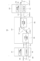
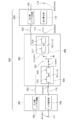
- FIG. 1 is a circuit configuration diagram showing a high frequency amplifier according to a first embodiment of the present technology. It is a circuit block diagram which shows the signal which flows through the high frequency amplifier of FIG. It is a schematic diagram which shows the output side impedance conversion part of the high frequency amplifier of FIG. It is a Smith chart figure which shows the movement of the impedance in the high frequency amplifier of FIG. It is a circuit block diagram which shows the high frequency amplifier of 2nd Embodiment which concerns on this technique. It is a schematic diagram which shows the output side impedance conversion part of the high frequency amplifier of FIG. It is a Smith chart figure which shows the motion of the impedance in the high frequency amplifier of FIG. It is a figure which shows the relationship between a Smith chart and an admittance chart.
- (A) is a Smith chart figure
- (B) is an admittance chart figure. It is a graph which shows the relationship between the insertion loss degradation amount of a connection part, and an impedance real part. It is a graph which shows the relationship of the variation
- High Frequency Amplifier According to First Embodiment (1-1) Example of Circuit Configuration of High Frequency Amplifier (1-2) Example of Operation of High Frequency Amplifier (1-3) Example of Configuration of Impedance Converter (1-4) Movement of Impedance 2. High Frequency Amplifier According to Second Embodiment (2-1) Example of Circuit Configuration of High Frequency Amplifier (2-2) Example of Configuration of Impedance Converter (2-3) Movement of Impedance (2-4) Relationship Between Impedance and Admittance 3. Example of high frequency amplifier to which the present technology is applied 4. Electronic Device of Third Embodiment Communication Device of Fourth Embodiment Application example of high frequency amplifier to which this technology is applied
- High-Frequency Amplifier of First Embodiment> A high frequency amplifier according to a first embodiment of the present technology will be described using FIGS. 1 to 4.
- the high frequency amplifier of the present embodiment is, for example, a high frequency amplifier which can be used for a front end circuit which is a transmitting / receiving end circuit on the antenna side for the fifth generation mobile communication system (5G).
- 5G fifth generation mobile communication system
- FIG. 1 is a circuit diagram showing the high frequency amplifier of this embodiment.
- the high frequency amplifier 100 includes a first substrate 101 which is an external substrate on the input side, a second substrate 102 of a circuit board made of semiconductor chips, and an external substrate which is an output side. 3 and a substrate 103.
- the first substrate 101 includes an input-side bias circuit 104 and an input matching unit 105 electrically connected to the input-side bias circuit 104.
- the input side bias circuit 104 is an electronic circuit for applying a bias voltage or a bias current on the input side.
- the input matching unit 105 is configured to match the impedance on the input side and the impedance in the circuit to, for example, 50 ⁇ .
- the second substrate 102 has an input-side impedance converter 106, which is a first impedance converter, a transistor 107, and an output-side impedance converter 108, which is a second impedance converter.
- the input impedance conversion unit 106 is electrically connected to the gate terminal of the transistor 107.
- the drain terminal of the transistor 107 is electrically connected to the output impedance conversion unit 108, and the source terminal of the transistor 107 is connected to the ground.
- the input impedance converter 106 and the output impedance converter 108 are configured to match the input impedance Zin of the high frequency amplifier 100 and the output impedance Zout of the high frequency amplifier 100 with the impedance of the transistor 107.
- the third substrate 103 includes an output side bias circuit 109 and an output matching unit 110 electrically connected to the output side bias circuit 109.
- the output side bias circuit 109 is an electronic circuit for applying a bias voltage or a bias current on the output side.
- the output matching unit 110 is configured to match the impedance in the circuit and the impedance on the output side to, for example, 50 ⁇ .
- the input terminal 111 of the high frequency amplifier 100 is connected to one end of the input matching unit 105.
- the other end of the input matching unit 105 is connected to the input-side impedance conversion unit 106 via the input-side connection unit 112 which is a first connection unit.
- the output impedance conversion unit 108 is connected to one end of the output matching unit 110 via the output connection unit 113 which is a second connection unit.
- the other end of the output matching unit 110 is connected to the output terminal 114 of the high frequency amplifier 100.
- a wire, a bump, or the like is used for the input side connection unit 112 and the output side connection unit 113.
- the high frequency amplifier 100 increases the output impedance real part of the transistor by the input impedance conversion unit 106 and / or the output impedance conversion unit 108 and then connects the input connection unit 112 / or the output connection unit 113. To reduce the influence of the connection.
- FIG. 2 is a circuit diagram showing signals flowing through the high frequency amplifier of this embodiment.
- an RF signal 201 is input to the input matching unit 105 via the input terminal 111 from, for example, a mixer or a quadrature modulator.
- the RF signal 201 input to the input matching unit 105 is input to the input impedance conversion unit 106 via the input connection unit 112, amplified from the input impedance conversion unit 106 via the transistor 107, and output impedance conversion It is input to the unit 108.
- the RF signal 201 amplified and input to the output impedance conversion unit 108 is input to the output matching unit 110 via the output connection unit 113. Then, the RF signal 201 input to the output matching unit 110 is output to, for example, an antenna via the output terminal 114.
- the input impedance of the transistor 107 is Z1i [ohm], and the impedance of the end point of the input side connection portion 112 on the second substrate 102 side is Z2i [ohm].
- the input impedance of the amplifier 100 is Zin [ohm].
- the output impedance of the transistor 107 is Z1o [ohm]
- the impedance of the end of the output side connection portion 113 on the second substrate 102 side is Z2o [ohm]
- the output impedance of the high frequency amplifier 100 is Zout [ ohm] is said.
- FIG. 3 is a schematic view showing the output side impedance converter of the high frequency amplifier of the present embodiment.
- the output impedance converter 108 includes a transmission line 301 and a capacitive element 302 electrically connected to the transmission line 301.
- the transmission line 301 is connected in series between the transistor-side input terminal 303 of the output-side impedance conversion unit 108 and the connection-side output terminal 304.
- the capacitive element 302 is branched and connected between the transmission line 301 and the connection section output terminal 304. Examples of the configuration of the capacitive element 302 include MIM capacitance + Backside VIA, capacitive open stubs, and the like.
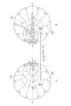
- FIG. 4 is a Smith chart showing the movement of the impedance of the output side impedance converter 108 of this embodiment.
- the concentric circular curve group 401 represents contour lines of the impedance real part
- the curve group 402 intersecting the curve group 401 represents contour lines of the impedance imaginary part.
- the left end of FIG. 4 shows 0 ⁇ and the right end shows ⁇ ⁇ , and the real part of impedance increases from the left end toward the right end.
- point P 0 in FIG. 4 is 25 ⁇ j * 25 ⁇ .
- a curve 403 from point P1 to point P2 in FIG. 4 represents the change in impedance due to the transmission line 301
- a curve 404 from point P2 to point P3 in FIG. 4 represents the change in impedance due to the capacitive element 302.
- the output impedance conversion unit 108 converts the impedance real part from point P1 to point P3 high without changing the imaginary part of impedance.
- the impedance imaginary part may change before and after conversion.
- the input matching unit 105 and the output matching unit 110 which are conventionally disposed in the second substrate 102 of the semiconductor chip, are the first external substrates. It is installed on the substrate 101 and the third substrate 103.
- This can reduce the size of a semiconductor chip using an expensive material such as a GaN substrate, which has a higher performance than the high frequency amplifier 100.
- the output impedance conversion unit 108 can reduce the impedance conversion ratio, it is not necessary to convert the impedance of the transistor 107 up to the input / output impedance of the high frequency amplifier 100, so the semiconductor chip can be miniaturized. Therefore, the second substrate 102 of the high frequency amplifier 100 can be miniaturized and the cost can be reduced without adjusting the wire length or the like of the output side connection portion 113.
- the high frequency amplifier 100 increases the impedance real part at the output side impedance conversion unit 108, the influence of the manufacturing variation at the output side connection unit 113 on the characteristics of the high frequency amplifier 100 can be reduced. it can.
- the high frequency amplifier 100 can suppress the influence of the manufacturing variation sufficiently even if the wire etc. is used between the semiconductor chip and the external substrate, so it is robust against the manufacturing variation (strong against the error factor) Design becomes possible.
- the impedance real part of the output side connection part 113 can be made higher than the terminal part of the transistor 107. Also in this case, the high frequency amplifier 100 can realize a robust design against manufacturing variations of the output side connection portion 113.
- manufacturing variation means that an inductance shifts
- High Frequency Amplifier of Second Embodiment> A high frequency amplifier according to a second embodiment of the present technology will be described with reference to FIGS. 5 to 8.
- the high frequency amplifier of the present embodiment is different from the high frequency amplifier 100 of the first embodiment in that a bias connection portion is connected in the middle of the impedance conversion portion in the second substrate.
- symbol is described in the structure similar to the structure of 1st Embodiment, and description is abbreviate
- FIG. 5 is a circuit configuration diagram showing the high frequency amplifier of the present embodiment.
- the high frequency amplifier 500 according to this embodiment includes a first substrate 501 which is an external substrate on the input side, a second substrate 502 made of a semiconductor chip, and a third substrate 503 which is an external substrate on the output side. And have.
- the first substrate 501 has an input side bias circuit 104 and an input matching unit 105. However, on the first substrate 501, the input side bias circuit 104 and the input matching unit 105 are not electrically connected.
- the second substrate 502 has an input impedance conversion unit 506 which is a first impedance conversion unit, a transistor 107, and an output impedance conversion unit 508 which is a second impedance conversion unit.
- the input impedance converter 506 is electrically connected to the gate terminal of the transistor 107.
- the drain terminal of the transistor 107 is electrically connected to the output impedance conversion unit 508, and the source terminal of the transistor 107 is connected to the ground.
- the input impedance conversion unit 506 includes two transmission lines 515 and a transmission line 516 connected in series.
- the output impedance transformation unit 508 has two transmission lines 517 and 518 connected in series.
- the number of transmission lines included in the input impedance conversion unit 506 and the output impedance conversion unit 508 is not limited to two but may be three or more.
- the third substrate 503 has an output side bias circuit 109 and an output matching unit 110. However, in the third substrate 503, the output side bias circuit 109 and the output matching unit 110 are not electrically connected.
- the input terminal 111 of the high frequency amplifier 500 is connected to one end of the input matching unit 105.
- the other end of the input matching unit 105 is connected to the input impedance conversion unit 506 via the input connection unit 112.
- the output impedance converter 508 is connected to one end of the output matching unit 110 via the output connector 113.
- the other end of the output matching unit 110 is connected to the output terminal 114 of the high frequency amplifier 500.
- the input-side bias circuit 104 is connected between the transmission line 515 and the transmission line 516 in the input-side impedance conversion unit 506 via the input-side bias connection unit 522.
- the output side bias circuit 109 is connected between the transmission line 517 and the transmission line 518 in the output side impedance conversion unit 508 via the output side bias connection unit 523.
- a wire, a bump or the like is used for the input side bias connection portion 522 and the output side bias connection portion 523.
- the input impedance of the transistor 107 is Z1i [ohm]
- the impedance of the end of the input-side connection unit 112 on the second substrate 502 side is Z2i [ohm]
- the output impedance of the transistor 107 is Z1 o [ohm]
- the impedance of the end of the output-side connecting portion 113 on the second substrate 502 side is Z2 o [ohm]
- the output impedance of the high frequency amplifier 500 is Z out [ohm].
- the input impedance of the branch point to the input side bias connection 522 between the transmission line 515 and the transmission line 516 is Z0i [ohm]
- the branch point to the output side bias circuit 109 between the transmission line 517 and the transmission line 518 is The output impedance is Z0 o [ohm].
- the high frequency amplifier 500 satisfies at least one of the above-described (Expression 1) or (Expression 2). Furthermore, the high frequency amplifier 500 satisfies at least one of the above (Equation 3) or (Equation 4).
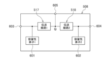
- FIG. 6 is a schematic view showing the output side impedance converter of the high frequency amplifier of the present embodiment.
- the output side impedance converter 508 includes two transmission lines 517 and 518 connected in series, and two capacitive elements 601 and 602.
- the transmission line 517 and the transmission line 518 are connected in series between the transistor-side input terminal 603 of the output-side impedance conversion unit 508 and the connection-side output terminal 604.
- the capacitive element 601 is branched and connected between the transistor side input terminal 603 and the transmission line 517.
- the capacitive element 602 is branched and connected between the transmission line 518 and the connection side output terminal 604.
- the branch point Q between the transmission line 517 and the transmission line 518 is connected to the bias connection side output terminal 605.
- the branch point Q indicates a feeding point.
- the impedance of the transistor-side input terminal 603 is 10-j * 10 [ohm]
- the impedance of the branch point Q which is a feeding point is 4 [ohm]
- the impedance of the connection-side output terminal 604 is , 30-j * 10 [ohm].
- FIG. 7 is a Smith chart diagram showing the movement of the impedance of the output side impedance converter 508 of this embodiment. Similar to FIG. 4, the concentric circular curve group 401 shown in the Smith chart of FIG. 7 represents contour lines of the impedance real part, and the curve group 402 intersecting the curve group 401 represents contour lines of the impedance imaginary part. ing.
- a curve 701 from point Q2 to point Q3 in FIG. 7 represents the change in impedance due to the transmission line 517
- a curve 702 from point Q3 to point Q4 in FIG. 7 represents the change in impedance due to the transmission line 518
- the curve 703 from point Q1 to point Q2 in FIG. 7 represents the change in impedance due to the capacitive element 601
- the curve 704 from point Q4 to point Q5 in FIG. 7 represents the change in impedance due to the capacitive element 602.
- the output impedance conversion unit 508 converts the real part of the impedance from point Q1 to point Q5 high without changing the imaginary part of impedance.
- the impedance imaginary part may change before and after conversion.
- FIG. 8 is a diagram showing the relationship between the Smith chart and the admittance chart.
- FIG. 8A is a Smith chart similar to FIG. 7, and
- FIG. 8B is an admittance chart corresponding to FIG. 8A.
- the concentric circular curve group 401 shown in the Smith chart of FIG. 8A represents the contour line of the impedance real part
- the curve group 402 intersecting the curve group 401 represents the contour line of the impedance imaginary part. ing.
- the reference impedance 50 [Omega, P A point 8A is a 25-j * 25 ⁇ .
- concentric circular curves 801 represent contours of the admittance real part
- curves 802 intersecting the curve group 801 represent contours of the admittance imaginary part.
- the right end of FIG. 8B is 0S and the left end is ⁇ S on the line segment in the left-right direction that represents the diameter of the circle of the admittance chart, and the admittance real part increases in size from the right end toward the left end.
- the reference impedance to 50 [ ⁇ ] 0.02 [S ]
- the input admittance of the transistor 107 is 1 / Z1i [S]
- the admittance at the end point (branch point) of the input side bias connection portion 522 on the second substrate 502 side is 1 / Z0i [S].
- the output admittance of the transistor 107 is 1 / Z1o [S]
- the admittance at the end point (branch point) of the output side bias connection portion 523 on the second substrate 502 side is 1 / Z0o [S].
- the high frequency amplifier 500 according to the present embodiment can reduce the size and cost of the second substrate 502 of the high frequency amplifier 500, similarly to the high frequency amplifier 100 according to the first embodiment. Further, in the high frequency amplifier 500, as in the high frequency amplifier 100 according to the first embodiment, the impedance real part is increased by the input impedance conversion unit 506 and / or the output impedance conversion unit 508 to sufficiently reduce the influence of manufacturing variations. Since it can be suppressed, a robust design is possible against manufacturing variations. Further, in the high frequency amplifier 500, as in the high frequency amplifier 100 according to the first embodiment, the impedance real part of the output side connection portion 113 can be made higher than the terminal portion of the transistor 107. Also in this case, the high frequency amplifier 500 can realize a robust design against manufacturing variations of the output side connection portion 113.
- the input impedance conversion unit 506 is configured such that the admittance real part of the input side bias connection unit 522 and / or the output side bias connection unit 523 is equal to or higher than the input / output admittance of the transistor 107.
- / or the output side impedance converter 508 is configured.
- Example of high frequency amplifier to which the present technology is applied An embodiment of a high frequency amplifier to which the present technology is applied will be described with reference to FIGS. 9 to 11.
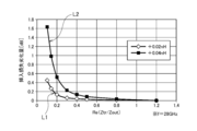
- FIG. 9 is a graph showing the relation between the insertion loss deterioration amount at the connection portion and the real part of the impedance.
- the horizontal axis in FIG. 9 shows the real part Re (Ztr / Zout) of the ratio of the output impedance (Ztr) of the transistor to the output impedance (Zout) of the high frequency amplifier, and the vertical axis in FIG.
- the insertion loss deterioration amount [dB] is shown.
- Zout 50 ⁇ is used as an example.
- the pass characteristic of the connection part is significantly reduced.
- the passage characteristic of the connection portion is significantly lower than the curve L1 in which the deviation is small. Therefore, it is necessary to enlarge the real part of the impedance immediately before the connection to reduce the influence of the connection (wire).
- FIG. 10 is a graph showing the relationship between the amount of change in the wire length of the connection portion of the high frequency amplifier to which the prior art is applied and the passage characteristic.
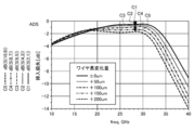
- FIG. 11 is a graph showing the relationship between the amount of change in the wire length of the connection portion of the high frequency amplifier to which the present technology is applied and the passage characteristic. 10 and 11, the horizontal axis represents frequency [GHz], and the vertical axis represents insertion loss [dB] from the output of the drain terminal of the transistor to the output of the high frequency amplifier (matching circuit).
- the curve C1 is the wire length change amount when the wire length change amount is ⁇ 0 um
- the curve C2 is the wire length change amount when the wire length change amount is +50 um, with respect to the original wire length 300 um.
- curve C4 represents a change in wire length of +150 um
- curve C5 represents a change in wire length of +200 um.
- the insertion loss at 28 GHz is degraded by about 1 dB with respect to ⁇ 0 um. From this, as shown by the curves C1 to C5 in FIG. 10, in the high frequency amplifier to which the prior art is applied, when the frequency becomes high, the influence of the manufacturing variation of the output side wire length becomes large by the change amount of the wire length. I understand that.
- the high frequency amplifier to which the present technology is applied can reduce the influence of the variation in the wire length on the output side due to the change in the wire length even if the frequency increases. I understand.
- the electronic device of the third embodiment according to the present technology is an electronic device provided with the high frequency amplifier according to any one of the first embodiment and the second embodiment according to the present technology.
- the high frequency amplifiers according to the first and second embodiments of the present technology are as described above, and thus the description thereof is omitted here.
- the electronic device according to the third embodiment of the present technology includes the high-frequency amplifier that is downsized and has excellent reliability, so that the performance of the electronic device can be reduced, and the performance can be improved.
- a communication device of a fourth embodiment according to the present technology is a device including the high frequency amplifier according to any one of the first embodiment and the second embodiment according to the present technology.
- the high frequency amplifiers according to the first and second embodiments of the present technology are as described above, and thus the description thereof is omitted here. Since the communication device of the fourth embodiment according to the present technology includes the high-frequency amplifier which is miniaturized and has excellent reliability, it is possible to improve the performance such as amplification of transmission and reception signals.
- Examples of communication devices according to the present embodiment include mobile communication terminals (mobile phones and smart phones), mobile communication base stations, other wireless stations, IoT devices, radars, and the like.
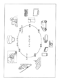
- FIG. 12 is a diagram showing an example of use of the high frequency amplifier according to the first and second embodiments of the present technology.
- the high frequency amplifiers according to the first and second embodiments described above may be used, for example, in various cases for sensing light such as visible light, infrared light, ultraviolet light, X-rays, etc. as described below. it can. That is, as shown in FIG. 12, for example, the field of viewing where images are provided for viewing, the field of transportation, the field of home appliances, the field of medical and healthcare, the field of security, the field of beauty, sports
- the high-frequency amplifier according to the first and second embodiments is used in an apparatus (for example, the electronic device according to the third embodiment described above) including a solid-state imaging device (image sensor) used in the field of agriculture, the field of agriculture, etc. can do.
- a device for capturing an image to be provided for viewing such as a digital camera, a smartphone, a mobile phone with a camera function, etc. includes the first embodiment and the second embodiment.
- the high frequency amplifier of the embodiment can be used.
- in-vehicle sensors for capturing images in front of, behind, around, inside of vehicles, etc., for monitoring safe driving such as automatic stop, etc., driving vehicles and roads.
- the high frequency amplifiers of the first embodiment and the second embodiment can be used in devices provided for traffic, such as surveillance cameras, distance measuring sensors for distance measurement between vehicles, etc.
- a device provided to home appliances such as a television receiver, a refrigerator, an air conditioner, etc. in order to photograph a user's gesture and perform device operation according to the gesture.
- the high frequency amplifier of the embodiment and the second embodiment can be used.
- devices provided for medical use and healthcare such as an endoscope and a device for performing blood vessel imaging by receiving infrared light are the first embodiment and the second embodiment.
- the high frequency amplifier of the embodiment can be used.
- the high frequency amplifier according to the first embodiment and the second embodiment for an apparatus provided for security, such as a surveillance camera for crime prevention and a camera for person authentication. it can.
- the high-frequency amplifier according to the first embodiment or the second embodiment is used for a device provided for beauty use, such as a skin measuring instrument for photographing the skin and a microscope for photographing the scalp. can do.
- the high-frequency amplifier according to the first and second embodiments can be used in devices provided for sports, such as action cameras and wearable cameras for sports applications and the like. .
- the high-frequency amplifier according to the first and second embodiments can be used in an apparatus used for agriculture, such as a camera for monitoring the condition of fields and crops. .
- the present technology can have the following configurations.
- At least one of the first substrate and the third substrate has a bias circuit, The high frequency amplifier according to (2), wherein the bias circuit is connected to the matching unit in a substrate having the bias circuit.
- the input (output) impedance of the transistor is Z1i (Z1o)
- the impedance of the end of the input (output) side connection on the second substrate side is Z2i (Z2o)
- the input (output) impedance of the amplifier is Zin (Zout)
- the high frequency amplifier according to (2) or (3) satisfying at least one of Re (Z1i) ⁇ Re (Z2i) ⁇ Re (Zin) or Re (Z1o) ⁇ Re (Z2o) ⁇ Re (Zout).
- the first impedance conversion unit has a transmission line connected in series to the first connection unit, and a capacitive element connected in parallel to the first connection unit in any one of (1) to (8).
- the high frequency amplifier as described in any one.
- Electronic equipment provided with the high frequency amplifier in any one of (1) to (9) which amplifies an input signal or an output signal.
- a communication device comprising the high frequency amplifier according to any one of (1) to (9), which amplifies a transmission signal or a reception signal.
Landscapes
- Engineering & Computer Science (AREA)
- Power Engineering (AREA)
- Computer Networks & Wireless Communication (AREA)
- Signal Processing (AREA)
- Microelectronics & Electronic Packaging (AREA)
- Amplifiers (AREA)
Abstract
L'invention concerne un amplificateur à haute fréquence pour lequel il est possible de miniaturiser une carte de circuit imprimé afin de réduire les coûts. L'amplificateur à haute fréquence comprend : une première carte comportant une unité d'adaptation ; et une deuxième carte comportant un transistor et une première unité de conversion d'impédance qui sont connectés l'un à l'autre, l'unité d'adaptation de la première carte et la première unité de conversion d'impédance étant connectées l'une à l'autre par l'intermédiaire d'une première unité de connexion. En outre, l'amplificateur à haute fréquence est par ailleurs pourvu d'une troisième carte comportant une unité d'adaptation, la deuxième carte étant en outre pourvue d'une seconde unité de conversion d'impédance connectée à un transistor, et la seconde unité de conversion d'impédance et l'unité d'adaptation de la troisième carte peuvent être connectées l'une à l'autre par l'intermédiaire d'une seconde unité de connexion.
Priority Applications (1)
| Application Number | Priority Date | Filing Date | Title |
|---|---|---|---|
| US16/766,282 US11336241B2 (en) | 2017-11-30 | 2018-09-12 | High-frequency amplifier, electronic device, and communication device |
Applications Claiming Priority (2)
| Application Number | Priority Date | Filing Date | Title |
|---|---|---|---|
| JP2017229882A JP2019102908A (ja) | 2017-11-30 | 2017-11-30 | 高周波増幅器、電子機器および通信機器 |
| JP2017-229882 | 2017-11-30 |
Publications (1)
| Publication Number | Publication Date |
|---|---|
| WO2019106909A1 true WO2019106909A1 (fr) | 2019-06-06 |
Family
ID=66664963
Family Applications (1)
| Application Number | Title | Priority Date | Filing Date |
|---|---|---|---|
| PCT/JP2018/033733 Ceased WO2019106909A1 (fr) | 2017-11-30 | 2018-09-12 | Amplificateur à haute fréquence, dispositif électronique et dispositif de communication |
Country Status (3)
| Country | Link |
|---|---|
| US (1) | US11336241B2 (fr) |
| JP (1) | JP2019102908A (fr) |
| WO (1) | WO2019106909A1 (fr) |
Citations (6)
| Publication number | Priority date | Publication date | Assignee | Title |
|---|---|---|---|---|
| JPS5757014A (en) * | 1980-09-24 | 1982-04-06 | Nec Corp | Superwide-band high output transistor amplifier |
| JPH04287507A (ja) * | 1991-03-18 | 1992-10-13 | Mitsubishi Electric Corp | 電界効果トランジスタ増幅器 |
| JPH065794A (ja) * | 1992-06-19 | 1994-01-14 | Hitachi Ltd | 高周波増幅装置 |
| JPH08293746A (ja) * | 1995-04-20 | 1996-11-05 | Hitachi Ltd | 高周波電力増幅器 |
| JP2005295193A (ja) * | 2004-03-31 | 2005-10-20 | Sumitomo Electric Ind Ltd | 電力増幅器 |
| JP2014120582A (ja) * | 2012-12-14 | 2014-06-30 | Sumitomo Electric Device Innovations Inc | 半導体装置 |
Family Cites Families (12)
| Publication number | Priority date | Publication date | Assignee | Title |
|---|---|---|---|---|
| JPH0279607A (ja) | 1988-09-16 | 1990-03-20 | Mitsubishi Electric Corp | マイクロ波増幅器 |
| US6999290B1 (en) * | 1999-04-28 | 2006-02-14 | Hitachi, Ltd. | Integrated circuit with protection against electrostatic damage |
| JP3892216B2 (ja) | 2000-08-22 | 2007-03-14 | 三菱電機株式会社 | マイクロ波増幅器 |
| JP2006129443A (ja) * | 2004-09-30 | 2006-05-18 | Renesas Technology Corp | 高周波電力増幅器 |
| JP4838572B2 (ja) * | 2005-11-24 | 2011-12-14 | 株式会社エヌ・ティ・ティ・ドコモ | 安定化回路、マルチバンド増幅回路 |
| JP2007267181A (ja) * | 2006-03-29 | 2007-10-11 | Matsushita Electric Ind Co Ltd | 高周波電力送信装置 |
| JP2010087934A (ja) * | 2008-09-30 | 2010-04-15 | Panasonic Corp | 整合回路、高周波電力増幅器および携帯電話機 |
| WO2014073134A1 (fr) * | 2012-11-09 | 2014-05-15 | パナソニック株式会社 | Dispositif à semi-conducteur |
| EP2814113B1 (fr) * | 2013-06-14 | 2019-08-07 | Ampleon Netherlands B.V. | Symétriseur de marchand et amplificateur de puissance l'utilisant |
| JP2017055224A (ja) | 2015-09-08 | 2017-03-16 | 株式会社東芝 | 高周波半導体装置 |
| US11258406B2 (en) * | 2016-11-25 | 2022-02-22 | Murata Manufacturing Co., Ltd. | Power amplifier circuit |
| US10411658B2 (en) * | 2016-12-14 | 2019-09-10 | Kabushiki Kaisha Toshiba | Semiconductor device |
-
2017
- 2017-11-30 JP JP2017229882A patent/JP2019102908A/ja active Pending
-
2018
- 2018-09-12 WO PCT/JP2018/033733 patent/WO2019106909A1/fr not_active Ceased
- 2018-09-12 US US16/766,282 patent/US11336241B2/en active Active
Patent Citations (6)
| Publication number | Priority date | Publication date | Assignee | Title |
|---|---|---|---|---|
| JPS5757014A (en) * | 1980-09-24 | 1982-04-06 | Nec Corp | Superwide-band high output transistor amplifier |
| JPH04287507A (ja) * | 1991-03-18 | 1992-10-13 | Mitsubishi Electric Corp | 電界効果トランジスタ増幅器 |
| JPH065794A (ja) * | 1992-06-19 | 1994-01-14 | Hitachi Ltd | 高周波増幅装置 |
| JPH08293746A (ja) * | 1995-04-20 | 1996-11-05 | Hitachi Ltd | 高周波電力増幅器 |
| JP2005295193A (ja) * | 2004-03-31 | 2005-10-20 | Sumitomo Electric Ind Ltd | 電力増幅器 |
| JP2014120582A (ja) * | 2012-12-14 | 2014-06-30 | Sumitomo Electric Device Innovations Inc | 半導体装置 |
Also Published As
| Publication number | Publication date |
|---|---|
| US20210265961A1 (en) | 2021-08-26 |
| JP2019102908A (ja) | 2019-06-24 |
| US11336241B2 (en) | 2022-05-17 |
Similar Documents
| Publication | Publication Date | Title |
|---|---|---|
| US9356330B1 (en) | Radio frequency (RF) couplers | |
| JP5861868B2 (ja) | 電子回路および電子回路の製造方法 | |
| US20110267194A1 (en) | Compact directional coupler using semiconductor process and mobile rfid reader transceiver system using the same | |
| CN101820096A (zh) | 具有2阶分集的紧凑型天线系统 | |
| TWI462387B (zh) | 用於方向耦合器之夾層結構 | |
| WO2020108386A1 (fr) | Module d'amplification de radiofréquences et terminal de communications | |
| CN101421931B (zh) | 天线装置及使用此天线装置的电子设备 | |
| CN205194822U (zh) | 无线电或功率传输天线、射频电路及包含其的电子设备 | |
| JP2010087934A (ja) | 整合回路、高周波電力増幅器および携帯電話機 | |
| KR20150124096A (ko) | 안테나 장치 및 이를 포함하는 전자 장치 | |
| KR101444551B1 (ko) | 전력 증폭 회로 및 그를 포함하는 프론트 엔드 모듈 | |
| US20210281236A1 (en) | Balun and Method for Manufacturing the Same | |
| TW200405615A (en) | Planar dual-pole antenna structure | |
| CN203813758U (zh) | 耦合电路及无线电传输链 | |
| JP6788011B2 (ja) | 補聴器 | |
| CN104022322B (zh) | 平衡非平衡转换器 | |
| JP2021129172A (ja) | インピーダンス変換器及び電子装置 | |
| CN106532268A (zh) | 一种天线结构及移动终端 | |
| JP2019102908A (ja) | 高周波増幅器、電子機器および通信機器 | |
| US9893025B2 (en) | High isolation wideband switch | |
| US20160226140A1 (en) | Antenna system for receiving and transmitting wireless signals | |
| CN106301399A (zh) | 移动终端、天线装置及射频前端发射器件 | |
| CN117525794A (zh) | 耦合器、射频前端模组和电子设备 | |
| KR100893683B1 (ko) | 하이브리드 커플러 | |
| CN114695332B (zh) | 一种射频放大器 |
Legal Events
| Date | Code | Title | Description |
|---|---|---|---|
| 121 | Ep: the epo has been informed by wipo that ep was designated in this application |
Ref document number: 18884775 Country of ref document: EP Kind code of ref document: A1 |
|
| NENP | Non-entry into the national phase |
Ref country code: DE |
|
| 122 | Ep: pct application non-entry in european phase |
Ref document number: 18884775 Country of ref document: EP Kind code of ref document: A1 |