WO2019106948A1 - Transistor de type à grille isolante - Google Patents
Transistor de type à grille isolante Download PDFInfo
- Publication number
- WO2019106948A1 WO2019106948A1 PCT/JP2018/036982 JP2018036982W WO2019106948A1 WO 2019106948 A1 WO2019106948 A1 WO 2019106948A1 JP 2018036982 W JP2018036982 W JP 2018036982W WO 2019106948 A1 WO2019106948 A1 WO 2019106948A1
- Authority
- WO
- WIPO (PCT)
- Prior art keywords
- region
- conductor
- impurity
- impurity region
- insulating film
- Prior art date
- Legal status (The legal status is an assumption and is not a legal conclusion. Google has not performed a legal analysis and makes no representation as to the accuracy of the status listed.)
- Ceased
Links
Images





Classifications
-
- H—ELECTRICITY
- H10—SEMICONDUCTOR DEVICES; ELECTRIC SOLID-STATE DEVICES NOT OTHERWISE PROVIDED FOR
- H10D—INORGANIC ELECTRIC SEMICONDUCTOR DEVICES
- H10D30/00—Field-effect transistors [FET]
- H10D30/60—Insulated-gate field-effect transistors [IGFET]
- H10D30/64—Double-diffused metal-oxide semiconductor [DMOS] FETs
- H10D30/66—Vertical DMOS [VDMOS] FETs
- H10D30/669—Vertical DMOS [VDMOS] FETs having voltage-sensing or current-sensing structures, e.g. emulator sections or overcurrent sensing cells
-
- H—ELECTRICITY
- H10—SEMICONDUCTOR DEVICES; ELECTRIC SOLID-STATE DEVICES NOT OTHERWISE PROVIDED FOR
- H10D—INORGANIC ELECTRIC SEMICONDUCTOR DEVICES
- H10D30/00—Field-effect transistors [FET]
- H10D30/60—Insulated-gate field-effect transistors [IGFET]
- H10D30/64—Double-diffused metal-oxide semiconductor [DMOS] FETs
- H10D30/66—Vertical DMOS [VDMOS] FETs
- H10D30/668—Vertical DMOS [VDMOS] FETs having trench gate electrodes, e.g. UMOS transistors
-
- H—ELECTRICITY
- H10—SEMICONDUCTOR DEVICES; ELECTRIC SOLID-STATE DEVICES NOT OTHERWISE PROVIDED FOR
- H10D—INORGANIC ELECTRIC SEMICONDUCTOR DEVICES
- H10D62/00—Semiconductor bodies, or regions thereof, of devices having potential barriers
- H10D62/80—Semiconductor bodies, or regions thereof, of devices having potential barriers characterised by the materials
- H10D62/83—Semiconductor bodies, or regions thereof, of devices having potential barriers characterised by the materials being Group IV materials, e.g. B-doped Si or undoped Ge
- H10D62/832—Semiconductor bodies, or regions thereof, of devices having potential barriers characterised by the materials being Group IV materials, e.g. B-doped Si or undoped Ge being Group IV materials comprising two or more elements, e.g. SiGe
- H10D62/8325—Silicon carbide
-
- H—ELECTRICITY
- H10—SEMICONDUCTOR DEVICES; ELECTRIC SOLID-STATE DEVICES NOT OTHERWISE PROVIDED FOR
- H10D—INORGANIC ELECTRIC SEMICONDUCTOR DEVICES
- H10D84/00—Integrated devices formed in or on semiconductor substrates that comprise only semiconducting layers, e.g. on Si wafers or on GaAs-on-Si wafers
- H10D84/101—Integrated devices comprising main components and built-in components, e.g. IGBT having built-in freewheel diode
- H10D84/141—VDMOS having built-in components
-
- H—ELECTRICITY
- H10—SEMICONDUCTOR DEVICES; ELECTRIC SOLID-STATE DEVICES NOT OTHERWISE PROVIDED FOR
- H10W—GENERIC PACKAGES, INTERCONNECTIONS, CONNECTORS OR OTHER CONSTRUCTIONAL DETAILS OF DEVICES COVERED BY CLASS H10
- H10W10/00—Isolation regions in semiconductor bodies between components of integrated devices
-
- H—ELECTRICITY
- H10—SEMICONDUCTOR DEVICES; ELECTRIC SOLID-STATE DEVICES NOT OTHERWISE PROVIDED FOR
- H10W—GENERIC PACKAGES, INTERCONNECTIONS, CONNECTORS OR OTHER CONSTRUCTIONAL DETAILS OF DEVICES COVERED BY CLASS H10
- H10W10/00—Isolation regions in semiconductor bodies between components of integrated devices
- H10W10/01—Manufacture or treatment
-
- H—ELECTRICITY
- H10—SEMICONDUCTOR DEVICES; ELECTRIC SOLID-STATE DEVICES NOT OTHERWISE PROVIDED FOR
- H10D—INORGANIC ELECTRIC SEMICONDUCTOR DEVICES
- H10D12/00—Bipolar devices controlled by the field effect, e.g. insulated-gate bipolar transistors [IGBT]
- H10D12/411—Insulated-gate bipolar transistors [IGBT]
- H10D12/441—Vertical IGBTs
- H10D12/461—Vertical IGBTs having non-planar surfaces, e.g. having trenches, recesses or pillars in the surfaces of the emitter, base or collector regions
- H10D12/481—Vertical IGBTs having non-planar surfaces, e.g. having trenches, recesses or pillars in the surfaces of the emitter, base or collector regions having gate structures on slanted surfaces, on vertical surfaces, or in grooves, e.g. trench gate IGBTs
-
- H—ELECTRICITY
- H10—SEMICONDUCTOR DEVICES; ELECTRIC SOLID-STATE DEVICES NOT OTHERWISE PROVIDED FOR
- H10D—INORGANIC ELECTRIC SEMICONDUCTOR DEVICES
- H10D62/00—Semiconductor bodies, or regions thereof, of devices having potential barriers
- H10D62/10—Shapes, relative sizes or dispositions of the regions of the semiconductor bodies; Shapes of the semiconductor bodies
- H10D62/102—Constructional design considerations for preventing surface leakage or controlling electric field concentration
- H10D62/103—Constructional design considerations for preventing surface leakage or controlling electric field concentration for increasing or controlling the breakdown voltage of reverse-biased devices
- H10D62/105—Constructional design considerations for preventing surface leakage or controlling electric field concentration for increasing or controlling the breakdown voltage of reverse-biased devices by having particular doping profiles, shapes or arrangements of PN junctions; by having supplementary regions, e.g. junction termination extension [JTE]
- H10D62/106—Constructional design considerations for preventing surface leakage or controlling electric field concentration for increasing or controlling the breakdown voltage of reverse-biased devices by having particular doping profiles, shapes or arrangements of PN junctions; by having supplementary regions, e.g. junction termination extension [JTE] having supplementary regions doped oppositely to or in rectifying contact with regions of the semiconductor bodies, e.g. guard rings with PN or Schottky junctions
-
- H—ELECTRICITY
- H10—SEMICONDUCTOR DEVICES; ELECTRIC SOLID-STATE DEVICES NOT OTHERWISE PROVIDED FOR
- H10D—INORGANIC ELECTRIC SEMICONDUCTOR DEVICES
- H10D64/00—Electrodes of devices having potential barriers
- H10D64/111—Field plates
- H10D64/117—Recessed field plates, e.g. trench field plates or buried field plates
-
- H—ELECTRICITY
- H10—SEMICONDUCTOR DEVICES; ELECTRIC SOLID-STATE DEVICES NOT OTHERWISE PROVIDED FOR
- H10D—INORGANIC ELECTRIC SEMICONDUCTOR DEVICES
- H10D64/00—Electrodes of devices having potential barriers
- H10D64/20—Electrodes characterised by their shapes, relative sizes or dispositions
- H10D64/27—Electrodes not carrying the current to be rectified, amplified, oscillated or switched, e.g. gates
- H10D64/311—Gate electrodes for field-effect devices
- H10D64/411—Gate electrodes for field-effect devices for FETs
- H10D64/511—Gate electrodes for field-effect devices for FETs for IGFETs
- H10D64/517—Gate electrodes for field-effect devices for FETs for IGFETs characterised by the conducting layers
- H10D64/519—Gate electrodes for field-effect devices for FETs for IGFETs characterised by the conducting layers characterised by their top-view geometrical layouts
-
- H—ELECTRICITY
- H10—SEMICONDUCTOR DEVICES; ELECTRIC SOLID-STATE DEVICES NOT OTHERWISE PROVIDED FOR
- H10D—INORGANIC ELECTRIC SEMICONDUCTOR DEVICES
- H10D84/00—Integrated devices formed in or on semiconductor substrates that comprise only semiconducting layers, e.g. on Si wafers or on GaAs-on-Si wafers
- H10D84/101—Integrated devices comprising main components and built-in components, e.g. IGBT having built-in freewheel diode
- H10D84/141—VDMOS having built-in components
- H10D84/143—VDMOS having built-in components the built-in components being PN junction diodes
-
- H—ELECTRICITY
- H10—SEMICONDUCTOR DEVICES; ELECTRIC SOLID-STATE DEVICES NOT OTHERWISE PROVIDED FOR
- H10W—GENERIC PACKAGES, INTERCONNECTIONS, CONNECTORS OR OTHER CONSTRUCTIONAL DETAILS OF DEVICES COVERED BY CLASS H10
- H10W72/00—Interconnections or connectors in packages
- H10W72/90—Bond pads, in general
- H10W72/921—Structures or relative sizes of bond pads
- H10W72/926—Multiple bond pads having different sizes
Definitions
- the present disclosure relates to a gate insulating transistor.
- the present application claims priority based on Japanese Patent Application No. 2017-230807, which is a Japanese patent application filed on November 30, 2017. The entire contents of the description of the Japanese patent application are incorporated herein by reference.
- Patent Document 1 JP-A-2014-150126 discloses a MOSFET (Metal Oxide Semiconductor Field Effect Transistor) having a main cell region and a sense cell region. An element isolation layer is formed between the main cell region and the sense cell region.
- MOSFET Metal Oxide Semiconductor Field Effect Transistor
- a gate insulating transistor includes an active region, a sense region, an isolation trench, a first insulating film, a first conductor, a second insulating film, and a second conductor.
- the sense region is spaced apart from the active region.
- the isolation trench surrounds the sense region and separates the sense region and the active region.
- the active region is separated from a first impurity region having a first conductivity type, a second impurity region provided on the first impurity region and having a second conductivity type different from the first conductivity type, and the first impurity region. And a third impurity region provided on the second impurity region and having the first conductivity type.
- the active region is provided with a first gate trench defined by the first side surface and the first bottom surface connected to the first side surface.
- the first side surface is composed of a first impurity region, a second impurity region, and a third impurity region.
- the first bottom surface is constituted by the first impurity region.
- the first insulating film is in contact with both the first side surface and the first bottom surface.
- the first conductor is provided on the first insulating film.
- the second insulating film is provided in the isolation trench.
- the second conductor is provided on the second insulating film.
- the isolation trench reaches the first impurity region.
- the first insulating film is made of the same material as the second insulating film.
- the first conductor is made of the same material as the second conductor and is electrically isolated from the second conductor.
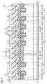
- FIG. 1 is a schematic cross-sectional view showing the configuration of the gate insulating transistor according to the first embodiment, and corresponds to a schematic cross-sectional view taken along the line II in FIG.
- FIG. 2 is a schematic plan view showing the configuration of the silicon carbide substrate of the gate insulating transistor according to the first embodiment.
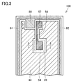
- FIG. 3 is a schematic plan view showing the configuration of the gate insulating transistor according to the first embodiment.
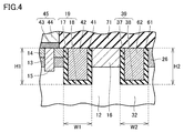
- FIG. 4 is an enlarged view of a region IV of FIG.
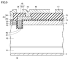
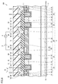
- FIG. 5 is a schematic cross-sectional view taken along line VV of FIG. 6 is a schematic cross-sectional view showing the configuration of the gate insulating transistor according to the second embodiment, and corresponds to the schematic cross-sectional view taken along the line VI-VI in FIG.
- FIG. 1 is a schematic cross-sectional view showing the configuration of the gate insulating transistor according to the first embodiment, and corresponds to a schematic cross-sectional view taken along the line II in FIG.
- FIG. 2 is a schematic
- FIG. 7 is a schematic plan view showing the configuration of the gate insulating transistor according to the second embodiment.
- FIG. 8 is a schematic cross-sectional view showing the configuration of the gate insulating transistor according to the third embodiment.
- FIG. 9 is a schematic cross-sectional view taken along the line XX in FIG.
- FIG. 10 is a schematic plan view showing the configuration of the gate insulating transistor according to the third embodiment.
- the element isolation layer is formed of an insulator such as an oxide.
- an insulator such as an oxide.
- An object of the present disclosure is to provide a gate insulating transistor capable of separating a sense region and an active region without significantly increasing the number of steps.
- the gate insulating transistor 100 includes the active region 10, the sense region 20, the isolation trench 39, the first insulating film 41, the first conductor 42, and the second insulating film 61. And a second conductor 62.
- Sense region 20 is spaced from active region 10.
- Isolation trench 39 surrounds sense region 20 and separates sense region 20 from active region 10.
- the active region 10 is provided with a first impurity region 12 having a first conductivity type, a second impurity region 13 provided on the first impurity region 12 and having a second conductivity type different from the first conductivity type, and a first impurity.
- a third impurity region 14 provided on second impurity region 13 and separated from region 12 and having the first conductivity type.
- the active region 10 is provided with a first gate trench 19 defined by the first side surface 17 and the first bottom surface 18 connected to the first side surface 17.
- the first side surface 17 is composed of a first impurity region 12, a second impurity region 13, and a third impurity region 14.
- the first bottom surface 18 is constituted by the first impurity region 12.
- an isolation trench 39 is provided in the isolation region 30.
- the first insulating film 41 is in contact with both the first side surface 17 and the first bottom surface 18.
- the first conductor 42 is provided on the first insulating film 41.
- the second insulating film 61 is provided in the isolation trench 39.
- the second conductor 62 is provided on the second insulating film 61.
- the isolation trench 39 reaches the first impurity region 12.
- the first insulating film 41 is made of the same material as the second insulating film 61.
- the first conductor 42 is made of the same material as the second conductor 62 and is electrically separated from the second conductor 62.
- the first gate trench 19 defined by the first side surface 17 and the first bottom surface 18 connected to the first side surface 17 is provided in the active region 10 ing.
- the isolation trench 39 isolates the sense region 20 and the active region 10. Thereby, sense region 20 and active region 10 are electrically separated.
- the first insulating film 41 is in contact with both the first side surface 17 and the first bottom surface 18.
- the first conductor 42 is provided on the first insulating film 41.
- the second insulating film 61 is provided in the isolation trench 39.
- the second conductor 62 is provided on the second insulating film 61.
- the first insulating film 41 is made of the same material as the second insulating film 61.
- the first conductor 42 is made of the same material as the second conductor 62.
- the isolation trench 39 can be formed simultaneously with the first gate trench 19. Therefore, sense region 20 and active region 10 can be separated without increasing the number of steps. Also, the isolation trench 39 can be easily filled. Furthermore, the separation trench 39 is filled with the second insulating film 61 and the second conductor 62, whereby generation of a step on the separation trench 39 can be suppressed. Therefore, when forming the aluminum wiring for supplying electric power to an electrode, it can suppress that the fault of the attachment circumference of the said wiring generate
- the sense region 20 may have the current sensor element 84.
- the gate insulating transistor 100 according to (2) may include the third insulating film 51 and the third conductor 52.
- Current sensor element 84 is provided on fourth impurity region 22 having fourth impurity region 22 having the first conductivity type and electrically connected to first impurity region 12 and having the second conductivity type.
- the fifth impurity region 23 may have a sixth impurity region 24 provided on the fifth impurity region 23 and separated from the fourth impurity region 22 and having the first conductivity type.
- a second gate trench 29 defined by the second side surface 27 and the second bottom surface 28 continuous with the second side surface 27 may be provided.
- the second side surface 27 may be configured by the fourth impurity region 22, the fifth impurity region 23, and the sixth impurity region 24.
- the second bottom surface 28 may be constituted by the fourth impurity region 22.
- the third insulating film 51 may be in contact with both the second side surface 27 and the second bottom surface 28.
- the third conductor 52 may be provided on the third insulating film 51.
- the first conductor 42 may be electrically connected to the third conductor 52.
- the sense region 20 may have a temperature sensor element 85.
- the gate insulating transistor 100 may include the source electrode 45 and the fourth conductor 95.
- Temperature sensor element 85 is provided on fourth impurity region 22 having fourth impurity region 22 having a first conductivity type and electrically connected to first impurity region 12 and having a second conductivity type. It may have the fifth impurity region 23 and the sixth impurity region 91 having the second conductivity type and having the impurity concentration higher than that of the fifth impurity region 23.
- Source electrode 45 may be electrically connected to third impurity region 14.
- the fourth conductor 95 may be electrically connected to each of the fifth impurity region 23 and the sixth impurity region 91.
- the source electrode 45 may be electrically separated from the fourth conductor 95.
- the depth of the isolation trench 39 may be equal to or greater than the depth of the first gate trench 19. Thereby, active region 10 and sense region 20 can be more reliably separated.
- the depth of the isolation trench 39 may be the same as the depth of the first gate trench 19.
- the width of the isolation trench 39 in the cross section perpendicular to the extending direction of the isolation trench 39 is the same as that of the first gate trench 19. It may be equal to or greater than the width of the first gate trench 19 in a cross section perpendicular to the extending direction. Active region 10 and sense region 20 can be more reliably separated.
- the material of the first conductor 42 and the second conductor 62 may be polysilicon.
- the sense region 20 may include the current sensor element 84 and the temperature sensor element 85.
- a boundary trench 67 may be provided to separate the current sensor element 84 and the temperature sensor element 85 and to be continuous with the separation trench 39.
- the MOSFET according to the first embodiment includes a silicon carbide substrate 9, a first insulating film 41, a third insulating film 51, a second insulating film 61, and a first conductor 42.
- Silicon carbide substrate 9 mainly has a first main surface 1, a second main surface 2, an active region 10, a sense region 20, and an isolation region 30.
- Sense region 20 is separated from active region 10.
- the separation region 30 is between the active region 10 and the sense region 20.
- Sense region 20 and active region 10 are separated from one another by isolation region 30.
- the second major surface 2 is on the opposite side of the first major surface 1.
- Each of the first major surface 1 and the second major surface 2 is constituted of an active region 10, a sense region 20 and an isolation region 30.
- Silicon carbide substrate 9 is made of, for example, hexagonal silicon carbide of polytype 4H.
- the first major surface 1 is a surface where the ⁇ 0001 ⁇ plane or the ⁇ 0001 ⁇ plane is inclined in the off direction by an off angle of 8 ° or less. Specifically, the first major surface 1 is a surface in which the (000-1) plane or the (000-1) plane is inclined in the off direction by an off angle of 8 ° or less.
- the off direction may be, for example, a ⁇ 11-20> direction or a ⁇ 1-100> direction.
- the off angle may be, for example, 1 ° or more, or 2 ° or more.
- the off angle may be 6 ° or less or 4 ° or less.
- the active region 10 includes a first drift region 12 (first impurity region 12), a first body region 13 (second impurity region 13), and a first source region 14 (third impurity).
- a region 14), a first contact region 15, a first p-type region 16, and a first substrate portion 11 are mainly included.
- First drift region 12 includes an n-type impurity such as nitrogen (N), for example, and has n-type (first conductivity type).
- the concentration of the n-type impurity in first drift region 12 is, for example, not less than 1 ⁇ 10 14 cm ⁇ 3 and not more than 5 ⁇ 10 16 cm ⁇ 3 .
- the first body region 13 is provided on the first drift region 12.
- First body region 13 includes a p-type impurity such as aluminum (Al), for example, and has a p-type (second conductivity type) different from n-type.
- the concentration of the p-type impurity in the first body region 13 may be higher than the concentration of the n-type impurity in the first drift region 12.
- the concentration of the p-type impurity in first body region 13 is, for example, not less than 1 ⁇ 10 16 cm ⁇ 3 and not more than 5 ⁇ 10 18 cm ⁇ 3 .
- the first source region 14 is provided on the first body region 13 so as to be separated from the first drift region 12.
- First source region 14 includes an n-type impurity such as nitrogen or phosphorus (P), for example, and has n-type.
- the first source region 14 constitutes, for example, a part of the first major surface 1.
- the concentration of the n-type impurity in the first source region 14 may be higher than the concentration of the p-type impurity in the first body region 13.
- the concentration of the n-type impurity in first source region 14 is, for example, about 1 ⁇ 10 19 cm ⁇ 3 .
- First contact region 15 includes a p-type impurity such as aluminum, for example, and has a p-type conductivity type.
- the concentration of the p-type impurity in the first contact region 15 is higher than, for example, the concentration of the p-type impurity in the first body region 13.
- the first contact region 15 penetrates, for example, each of the first body region 13 and the first source region 14.
- the first contact region 15 contacts, for example, the first drift region 12.
- First contact region 15 constitutes, for example, a part of first main surface 1.
- the concentration of the p-type impurity in the first contact region 15 is, for example, not less than 1 ⁇ 10 18 cm ⁇ 3 and not more than 1 ⁇ 10 20 cm ⁇ 3 .
- First p-type region 16 includes a p-type impurity such as aluminum, for example, and has p-type.
- the first p-type region 16 is provided on the first drift region 12.
- First p-type region 16 includes a p-type impurity such as aluminum, for example, and has p-type.
- the concentration of the p-type impurity in the first p-type region 16 may be the same as the concentration of the p-type impurity in the first body region 13.
- First p-type region 16 may be in contact with isolation region 30, for example.
- the first p-type region 16 may be connected to the source electrode 45 (S1).
- First substrate portion 11 includes an n-type impurity such as nitrogen (N), for example, and has an n-type (first conductivity type).
- the first substrate portion 11 constitutes, for example, a part of the second major surface 2.
- the concentration of the n-type impurity in the first substrate portion 11 may be higher than the concentration of the n-type impurity in the first drift region 12.
- the first drift region 12 is provided, for example, on the first substrate portion 11.
- the active region 10 is provided with a first gate trench 19 defined by the first side surface 17 and the first bottom surface 18.
- the first bottom surface 18 is continuous with the first side surface 17.
- the first side surface 17 is composed of a first drift region 12, a first body region 13, and a first source region 14.
- the first bottom surface 18 is constituted by the first drift region 12.
- the first side surface 17 penetrates each of the first body region 13 and the first source region 14 to reach the first drift region 12.
- the first bottom surface 18 is, for example, a plane parallel to the second major surface 2.
- the angle of the first side surface 17 with respect to the first bottom surface 18 is, for example, 90 °.
- the first side surface 17 may be inclined with respect to a plane perpendicular to the first bottom surface 18.
- the first side surface 17 may be inclined with respect to the first bottom surface 18 so that the width of the first gate trench 19 is expanded from the first bottom surface 18 toward the first main surface 1.
- the first gate trenches 19 extend in a stripe shape, for example, in a direction parallel to the second major surface 2.
- the first gate trenches 19 may extend in a honeycomb shape, for example, or may be scattered in an island shape.
- the first insulating film 41 is, for example, a gate oxide film.
- the first insulating film 41 is made of, for example, a material containing silicon dioxide.
- the first insulating film 41 is in contact with both the first side surface 17 and the first bottom surface 18.
- the first insulating film 41 is in contact with the first drift region 12 at the first bottom surface 18.
- the first insulating film 41 is in contact with each of the first drift region 12, the first body region 13 and the first source region 14 on the first side surface 17.
- the first conductor 42 is, for example, a first gate electrode.
- the first conductor 42 is provided on the first insulating film 41.
- the first conductor 42 is made of, for example, polysilicon containing a conductive impurity.
- the first conductor 42 is disposed, for example, inside the first gate trench 19.
- the first source electrode 45 (first electrode 45) is electrically connected to the first source region 14.
- First source electrode 45 is in contact with each of first source region 14 and first contact region 15 on first main surface 1, for example.
- the first source electrode 45 has a first contact electrode 43 and a first source wiring 44.
- the first source wiring 44 is provided on the first contact electrode 43.
- the first contact electrode 43 may be in contact with each of the first source region 14 and the first contact region 15 on the first major surface 1.
- the first contact electrode 43 is made of, for example, a material containing Ti, Al, and Si.
- the first contact electrode 43 is in ohmic contact with, for example, the first source region 14.
- the first contact electrode 43 may be in ohmic contact with the first contact region 15.
- First source interconnection 44 is made of, for example, a material containing aluminum.
- an isolation trench 39 is provided.
- the isolation trench 39 is defined by the third side surface 37 and the third bottom surface 38.
- the third bottom surface 38 is continuous with the third side surface 37.
- Isolation region 30 has, for example, third drift region 32 and third substrate portion 31.
- the third bottom surface 38 is constituted by the third drift region 32.
- the third bottom surface 38 is, for example, a plane parallel to the second major surface 2.
- the angle of the third side surface 37 with respect to the third bottom surface 38 is, for example, 90 °.
- the third side surface 37 may be inclined with respect to a plane perpendicular to the third bottom surface 38.
- the third side surface 37 may be inclined with respect to the first bottom surface 18 so that the width of the isolation trench 39 is expanded from the third bottom surface 38 toward the first main surface 1.
- the isolation trench 39 reaches the first impurity region 12. From another point of view, a part of the third side surface 37 of the isolation trench 39 is in contact with the first impurity region 12.
- the isolation trench 39 is sandwiched between the first p-type region 16 and the second p-type region 26. The isolation trench 39 is in contact with each of the first p-type region 16 and the second p-type region 26.
- the second insulating film 61 is, for example, an oxide film.
- the second insulating film 61 is made of, for example, a material containing silicon dioxide.
- the first insulating film 41 is made of the same material as the second insulating film 61.
- the second insulating film 61 is provided in the isolation trench 39.
- the second insulating film 61 is in contact with both the third side surface 37 and the third bottom surface 38.
- the second insulating film 61 is in contact with the third drift region 32 at the third bottom surface 38.
- the second insulating film 61 is in contact with each of the first p-type region 16 and the first drift region 12 on the third side surface 37, for example.
- the second conductor 62 is provided on the second insulating film 61.
- the second conductor 62 is made of, for example, polysilicon containing a conductive impurity.
- the second conductor 62 is disposed, for example, inside the isolation trench 39.
- the first conductor 42 is made of the same material as the second conductor 62.
- the first conductor 42 is electrically separated from the second conductor 62. From another point of view, the second conductor 62 is a floating electrode.
- the isolation trench 39 surrounds the sense region 20 as viewed in the direction perpendicular to the first major surface 1.
- the isolation trench 39 isolates the sense region 20 and the active region 10.
- Isolation trench 39 is provided in isolation region 30.
- isolation region 30 surrounds, for example, the outer periphery of sense region 20.
- the separation region 30 is, for example, annular.
- Active region 10 surrounds, for example, the outer periphery of separation region 30.
- Active region 10 is, for example, annular.
- sense region 20 has, for example, a rectangular shape.
- Sense region 20 includes, for example, a current sensor element 84.
- the sense region 20 includes a second drift region 22 (fourth impurity region 22), a second body region 23 (fifth impurity region 23), and a second source region 24 (sixth impurity).
- a region 24), a second contact region 25, a second p-type region 26, and a second substrate portion 21 are mainly included.
- the second drift region 22, the second body region 23, and the second source region 24 constitute, for example, a current sensor element 84.
- Second drift region 22 includes an n-type impurity such as nitrogen, for example, and has an n-type (first conductivity type).
- the second drift region 22 is electrically connected to the first drift region 12.
- the concentration of the n-type impurity in the second drift region 22 may be the same as the concentration of the n-type impurity in the first drift region 12.
- Second body region 23 includes p-type impurities such as aluminum (Al), for example, and has p-type.
- the second body region 23 is provided on the second drift region 22.
- the concentration of the p-type impurity in the second body region 23 may be higher than the concentration of the n-type impurity in the second drift region 22.
- the concentration of the p-type impurity in the second body region 23 may be the same as the concentration of the p-type impurity in the first body region 13.
- Second body region 23 is electrically separated, for example, from first body region 13.
- the second source region 24 is provided on the second body region 23 to be separated from the second drift region 22.
- Second source region 24 includes an n-type impurity such as nitrogen or phosphorus (P), for example, and has n-type.
- Second source region 24 constitutes, for example, a part of first main surface 1.
- the concentration of the n-type impurity in the second source region 24 may be higher than the concentration of the p-type impurity in the second body region 23.
- the concentration of the n-type impurity in the second source region 24 may be the same as the concentration of the n-type impurity in the first source region 14.
- the second source region 24 is electrically isolated from, for example, the first source region 14.
- Second contact region 25 includes a p-type impurity such as aluminum, for example, and has a p-type conductivity.
- the concentration of the p-type impurity in the second contact region 25 is higher than, for example, the concentration of the p-type impurity in the second body region 23.
- the second contact region 25 penetrates, for example, each of the second body region 23 and the second source region 24.
- Second contact region 25 contacts, for example, second drift region 22.
- Second contact region 25 constitutes, for example, a part of first main surface 1.
- the concentration of the p-type impurity in the second contact region 25 may be the same as the concentration of the p-type impurity in the first contact region 15.
- Second contact region 25 is electrically isolated from, for example, first contact region 15.
- the second p-type region 26 is provided on the second drift region 22.
- the second p-type region 26 contains p-type impurities such as aluminum, for example, and has p-type.
- the concentration of the p-type impurity in the second p-type region 26 may be the same as the concentration of the p-type impurity in the second body region 23.
- the second p-type region 26 may be in contact with, for example, the third side surface 37 of the isolation trench 39.
- the second substrate portion 21 contains n-type impurities such as nitrogen, for example, and has n-type. Second substrate portion 21 constitutes, for example, a part of second main surface 2.
- the concentration of the n-type impurity in the second substrate portion 21 may be higher than the concentration of the n-type impurity in the second drift region 22.
- Second drift region 22 is provided, for example, on second substrate portion 21.
- the second substrate portion 21 is continuous with the first substrate portion 11.
- a second gate trench 29 defined by the second side surface 27 and the second bottom surface 28 may be provided.
- the second bottom surface 28 is continuous with the second side surface 27.
- the second side surface 27 includes, for example, a second drift region 22, a second body region 23, and a second source region 24.
- the second bottom surface 28 is constituted by, for example, a second drift region 22.
- the second side surface 27 penetrates each of the second body region 23 and the second source region 24 to reach the second drift region 22.
- the second bottom surface 28 is, for example, a plane parallel to the second major surface 2.
- the angle of the first side surface 17 with respect to the second bottom surface 28 is, for example, 90 °.
- the second side surface 27 may be inclined with respect to a plane perpendicular to the second bottom surface 28.
- the second side surface 27 may be inclined with respect to the second bottom surface 28 so that the width of the second gate trench 29 is expanded from the second bottom surface 28 toward the first main surface 1.
- Second gate trench 29 extends in a stripe shape, for example, in a direction parallel to second main surface 2.
- the second gate trenches 29 may extend in a honeycomb shape, for example, or may be scattered in an island shape.
- the third insulating film 51 is, for example, a gate oxide film.
- Third insulating film 51 is made of, for example, a material containing silicon dioxide.
- the third insulating film 51 is in contact with both the second side surface 27 and the second bottom surface 28, for example.
- the third insulating film 51 is in contact with the second drift region 22 at the second bottom surface 28.
- the third insulating film 51 is in contact with each of the second drift region 22, the second body region 23, and the second source region 24 at the second side surface 27.
- the third conductor 52 is, for example, a second gate electrode.
- the third conductor 52 may be provided on the third insulating film 51.
- the third conductor 52 is made of, for example, polysilicon containing a conductive impurity.
- the third conductor 52 is disposed, for example, inside the second gate trench 29.
- the first conductor 42 is electrically connected to the third conductor 52.
- the materials of the first conductor 42 and the second conductor 62 are the same.
- the materials of the first conductor 42 and the third conductor 52 may also be the same.
- the second source electrode 55 is electrically connected to the second source region 24.
- Second source electrode 55 is in contact with each of second source region 24 and second contact region 25 on first main surface 1, for example.
- the second source electrode 55 has a second contact electrode 53 and a second source wire 54.
- the second source wiring 54 is provided on the second contact electrode 53.
- the second contact electrode 53 may be in contact with each of the second source region 24 and the second contact region 25 on the first major surface 1.
- the second contact electrode 53 is made of, for example, a material containing Ti, Al, and Si.
- the second contact electrode 53 is in ohmic contact with, for example, the second source region 24.
- the second contact electrode 53 may be in ohmic contact with the second contact region 25.
- Second source interconnection 54 is made of, for example, a material containing aluminum.
- the first source electrode 45 is electrically separated from, for example, the second source electrode 55.
- First interlayer insulating film 71 is provided, for example, to cover each of first gate trench 19 and isolation trench 39.
- the first interlayer insulating film 71 is provided in contact with, for example, the first conductor 42, the first insulating film 41, the second conductor 62, and the second insulating film 61.
- First interlayer insulating film 71 may be in contact with first source region 14, first p-type region 16, and second p-type region 26 on first main surface 1.
- First interlayer insulating film 71 may be provided on each of active region 10, sense region 20 and isolation region 30.
- the second interlayer insulating film 72 is provided to cover, for example, the second gate trench 29.
- the second interlayer insulating film 72 is provided in contact with, for example, the third conductor 52 and the third insulating film 51.
- the second interlayer insulating film 72 may be in contact with the second source region 24 on the first major surface 1.
- Second interlayer insulating film 72 is provided, for example, on sense region 20, and may be separated from each of active region 10 and isolation region 30.
- first interlayer insulating film 71 and second interlayer insulating film 72 is made of, for example, a material containing silicon dioxide.
- First interlayer insulating film 71 electrically insulates, for example, first conductor 42 and first source electrode 45.
- the second interlayer insulating film 72 electrically insulates, for example, the third conductor 52 and the second source electrode 55.
- the passivation layer 73 is provided in contact with the first source electrode 45, the second source electrode 55, and the first interlayer insulating film 71.
- Passivation layer 73 is made of, for example, a material such as silicon nitride (SiN), silicon dioxide or polyimide.
- drain electrode 70 (second electrode 70) is in contact with the second major surface 2. From another point of view, drain electrode 70 is in contact with each of first substrate portion 11, second substrate portion 21 and third substrate portion 31 on second main surface 2. The drain electrode 70 is electrically connected to each of the first drift region 12, the second drift region 22, and the third drift region 32. Drain electrode 70 is made of, for example, a material containing NiSi or TiAlSi. The drain electrode 70 is provided to cover each of the active region 10, the sense region 20, and the separation region 30.
- the MOSFET according to the first embodiment further includes a gate pad 80, a first gate runner 81, a second gate runner 82, a source pad 57, and a source wiring region 56. It may be
- the first gate runner 81 is connected to one side of the gate pad 80.
- the second gate runner 82 is connected to the other side of the gate pad 80.
- each of the first source wire 44, the source pad 57 and the source wire region 56 includes a first gate runner 81 and a second gate runner 81. It is sandwiched between the gate runner 82 and the like.
- Gate pad 80 is electrically connected to each of first conductor 42 and third conductor 52.
- the first source wire 44 is electrically separated from the second source wire 54.
- the source pad 57 is connected to the second source wire 54 via the source wire region 56.
- the source pad 57 is located next to the gate pad 80.
- Source pad 57 is electrically isolated from gate pad 80.
- the second source wire 54 may be surrounded by the isolation region 30.
- the second source wire 54 is disposed on the sense region 20.
- Source pad 57 may be disposed on active region 10.
- Source interconnection region 56 may be disposed on each of active region 10, isolation region 30 and sense region 20. When viewed in the direction perpendicular to second main surface 2, source interconnection region 56 may be provided to cross isolation region 30 in the direction substantially perpendicular to the extension direction of isolation region 30.
- Each of the gate pad 80, the first gate runner 81, the second gate runner 82, and the first source wiring 44 is disposed on the active region 10, for example.
- the depth H 2 of the isolation trench 39 may be equal to or greater than the depth H 1 of the first gate trench 19.
- the depth of the isolation trench 39 may be the same as the depth H 1 of the first gate trench 19 or may be larger than the depth H 1 of the first gate trench 19.
- the depth H1 of the first gate trench 19 is, for example, not less than 0.5 ⁇ m and not more than 3.0 ⁇ m.
- the depth H2 of the isolation trench 39 is, for example, not less than 0.5 ⁇ m and not more than 20.0 ⁇ m.
- the depth of the isolation trench 39 may be the same as the depth of the second gate trench 29 or may be larger than the depth of the second gate trench 29.
- the width W2 of the isolation trench 39 in a cross section perpendicular to the extending direction of the isolation trench 39 is a first gate trench in a cross section perpendicular to the extending direction of the first gate trench 19. It may be 19 or more in width W1.
- the width W 2 of the isolation trench 39 may be the same as the width W 1 of the first gate trench 19 or may be larger than the width W 1 of the first gate trench 19.
- the width W1 of the first gate trench 19 is, for example, not less than 0.2 ⁇ m and not more than 2.0 ⁇ m.
- the width W2 of the isolation trench 39 is, for example, not less than 0.2 ⁇ m and not more than 200 ⁇ m.
- the width of the isolation trench 39 may be the same as the width of the second gate trench 29 or may be larger than the width of the second gate trench 29.
- the extending direction of the trench is a direction parallel to the bottom of the trench and a direction parallel to the side of the trench.
- the MOSFET according to the first embodiment further includes a gate connection wiring 83, a first insulating layer 74, a second insulating layer 75, and a third interlayer insulating film 76. It is also good.
- Active region 10 may further include third p-type region 5.
- the third p-type region 5 is provided on the first drift region 12.
- Third p-type region 5 includes a p-type impurity such as aluminum, for example, and has p-type.
- the concentration of the p-type impurity in the third p-type region 5 may be the same as the concentration of the p-type impurity in the first body region 13.
- Third p-type region 5 may be in contact with first side surface 17 of first gate trench 19, for example.
- the first insulating layer 74 is disposed on the third p-type region 5.
- the first insulating layer 74 is in contact with the third p-type region 5 on the first major surface 1.
- the gate connection wiring 83 is disposed on the first conductor 42.
- the gate connection wiring 83 connects the first conductor 42 and the gate pad 80.
- the gate pad 80 is in contact with the gate connection wiring 83.
- the gate connection wiring 83 may be disposed on the first insulating layer 74.
- the first insulating layer 74 may be in contact with the first insulating film 41.
- the gate connection wiring 83 may be disposed between the gate pad 80 and the first insulating layer 74.
- the second insulating layer 75 is disposed, for example, on the first insulating layer 74.
- the second insulating layer 75 may be in contact with the gate connection wiring 83.
- Third interlayer insulating film 76 is disposed, for example, between first source electrode 45 and gate connection wiring 83.
- Third interlayer insulating film 76 electrically insulates, for example, first source electrode 45 and gate connection wiring 83.
- the third interlayer insulating film 76 may be disposed on the gate connection wiring 83.
- Gate pad 80 may be disposed on each of third interlayer insulating film 76 and second insulating layer 75. The gate pad 80 may be disposed to face the third p-type region 5.
- the first source wiring 44 is connected to the first source terminal S1.
- the second source wiring 54 is connected to the second source terminal S2.
- the drain electrode 70 is connected to the drain terminal D.
- the first gate electrode 42 is connected to the first gate terminal G1.
- the second gate electrode 52 is connected to the second gate terminal G2.
- the first gate terminal G1 is electrically connected to the second gate terminal G2.
- a current flows between the first source terminal S1 and the drain terminal D, and between the second source terminal S2 and the drain terminal D Current flows to The current flowing between the second source terminal S2 and the drain terminal D is substantially proportional to the current flowing between the first source terminal S1 and the drain terminal D. For example, when a current of 100 A flows between the first source terminal S1 and the drain terminal D, a current of 1 mA flows between the second source terminal S2 and the drain terminal D.
- the current flowing between the second source terminal S2 and the drain terminal D can be adjusted by changing the number of cells, the gate width, and the like.
- the relational expression between the current flowing between the second source terminal S2 and the drain terminal D and the current flowing between the first source terminal S1 and the drain terminal D is previously obtained.
- the current flowing between the second source terminal S2 and the drain terminal D is monitored by an ammeter (not shown).
- the current flowing between the first source terminal S1 and the drain terminal D is estimated based on the above relational expression. For example, when the current flowing between the second source terminal S2 and the drain terminal D exceeds a predetermined value, the MOSFET 100 may be controlled to stop the application of the gate voltage.
- the active region 10 is provided with the first gate trench 19 defined by the first side surface 17 and the first bottom surface 18 connected to the first side surface 17.
- the isolation trench 39 isolates the sense region 20 and the active region 10. Thereby, sense region 20 and active region 10 are electrically separated.
- the first insulating film 41 is in contact with both the first side surface 17 and the first bottom surface 18.
- the first conductor 42 is provided on the first insulating film 41.
- the second insulating film 61 is provided in the isolation trench 39.
- the second conductor 62 is provided on the second insulating film 61.
- the first insulating film 41 is made of the same material as the second insulating film 61.
- the first conductor 42 is made of the same material as the second conductor 62 and is electrically separated from the second conductor 62.
- the isolation trench 39 can be formed simultaneously with the first gate trench 19. Therefore, sense region 20 and active region 10 can be separated without increasing the number of steps. Also, the isolation trench 39 can be easily filled.
- the separation trench 39 is filled with the second insulating film 61 and the second conductor 62, whereby generation of a step on the separation trench 39 can be suppressed. Therefore, when forming the aluminum wiring for supplying electric power to an electrode, it can suppress that the fault of the attachment circumference of the said wiring generate
- the depth of the isolation trench 39 may be equal to or larger than the depth of the first gate trench 19. Thereby, active region 10 and sense region 20 can be more reliably separated.
- the width of the isolation trench 39 in the cross section perpendicular to the extending direction of the isolation trench 39 is the same as the width in the cross section perpendicular to the extending direction of the first gate trench 19.
- the width may be equal to or greater than the width of one gate trench 19. Active region 10 and sense region 20 can be more reliably separated.
- the MOSFET according to the second embodiment is different from the MOSFET according to the first embodiment in the configuration having a temperature sensor instead of the current sensor element, and the other configuration is the MOSFET according to the first embodiment. It is almost the same as The following description will focus on configurations that are different from the MOSFET according to the first embodiment.
- the sense region 20 may have a temperature sensor element. As shown in FIG. 6, the sense region 20 includes a fourth impurity region 22, a fifth impurity region 23, a third contact region 91 (sixth impurity region 91), a fourth contact region 92, and a second It mainly has a substrate portion 21.
- the fifth impurity region 23, the third contact region 91, and the fourth contact region 92 constitute, for example, a temperature sensor element 85.
- Temperature sensor element 85 is, for example, an electric resistor. The temperature dependency of the electrical resistor can be used to estimate the temperature from the resistance value of the electrical resistor.
- Fourth impurity region 22 includes an n-type impurity such as nitrogen, for example, and has an n-type (first conductivity type).
- the fourth impurity region 22 is electrically connected to the first drift region 12.
- the concentration of the n-type impurity of the fourth impurity region 22 may be the same as the concentration of the n-type impurity of the first drift region 12.
- the fifth impurity region 23 includes a p-type impurity such as aluminum (Al), for example, and has a p-type.
- the fifth impurity region 23 is provided on the fourth impurity region 22.
- the concentration of the p-type impurity in the fifth impurity region 23 may be higher than the concentration of the n-type impurity in the fourth impurity region 22.
- the concentration of the p-type impurity in the fifth impurity region 23 may be the same as the concentration of the p-type impurity in the first body region 13.
- Fifth impurity region 23 may be in contact with third side surface 37 of isolation trench 39, for example.
- Fifth impurity region 23 is electrically isolated from, for example, first body region 13.
- Each of third contact region 91 and fourth contact region 92 includes a p-type impurity such as aluminum, for example, and has a p-type conductivity type.
- the concentration of the p-type impurity of each of the third contact region 91 and the fourth contact region 92 is higher than, for example, the concentration of the p-type impurity of the fifth impurity region 23.
- Each of third contact region 91 and fourth contact region 92 is in contact with fifth impurity region 23.
- Each of third contact region 91 and fourth contact region 92 constitutes, for example, a part of first main surface 1.
- the concentration of the p-type impurity of each of the third contact region 91 and the fourth contact region 92 may be the same as the concentration of the p-type impurity of the first contact region 15.
- the second substrate portion 21 contains n-type impurities such as nitrogen, for example, and has n-type.
- Second substrate portion 21 constitutes, for example, a part of second main surface 2.
- the concentration of the n-type impurity in the second substrate portion 21 may be higher than the concentration of the n-type impurity in the fourth impurity region 22.
- Fourth impurity region 22 is provided, for example, on second substrate portion 21.
- the second substrate portion 21 is continuous with the third substrate portion 31.
- the MOSFET according to the second embodiment further includes a fourth conductor 95 and a fourth electrode 98.
- the fourth conductor 95 is a third electrode.
- the fourth conductor 95 is electrically connected, for example, to each of the fifth impurity region 23, the third contact region 91, and the fourth contact region 92.
- Fourth conductor 95 is in contact with third contact region 91, for example, on first main surface 1.
- the fourth conductor 95 has a third contact electrode 93 and a third wiring 94.
- the third wiring 94 is provided on the third contact electrode 93.
- the third contact electrode 93 may be in contact with the third contact region 91 on the first major surface 1.
- the third contact electrode 93 is made of, for example, a material containing Ti, Al, and Si.
- the third contact electrode 93 may be in ohmic contact with the third contact region 91.
- Third interconnection 94 is made of, for example, a material containing aluminum.
- the fourth conductor 95 can be connected to, for example,
- the fourth electrode 98 is electrically connected to each of, for example, the fifth impurity region 23, the third contact region 91, and the fourth contact region 92.
- the fourth electrode 98 is in contact with the fourth contact region 92 on the first major surface 1.
- the fourth electrode 98 has a fourth contact electrode 96 and a fourth wiring 97.
- the fourth wiring 97 is provided on the fourth contact electrode 96.
- the fourth contact electrode 96 may be in contact with the fourth contact region 92 on the first major surface 1.
- the fourth contact electrode 96 is made of, for example, a material containing Ti, Al, and Si.
- the fourth contact electrode 96 may be in ohmic contact with the fourth contact region 92.
- the fourth wiring 97 is made of, for example, a material containing aluminum.
- the fourth electrode 98 can be connected to, for example, the ammeter 4.
- the first source electrode 45 is electrically separated from each of the fourth conductor 95 and the fourth electrode 98.
- the second interlayer insulating film 72 is provided to cover a part of the first major surface 1.
- Second interlayer insulating film 72 is provided on first main surface 1 in contact with, for example, each of fifth impurity region 23, third contact region 91 and fourth contact region 92.
- Second interlayer insulating film 72 is provided, for example, on sense region 20, and may be separated from each of active region 10 and isolation region 30.
- Second interlayer insulating film 72 is made of, for example, a material containing silicon dioxide.
- Second interlayer insulating film 72 is positioned, for example, between fourth conductor 95 and fourth electrode 98.
- the MOSFET according to the second embodiment may further include a third pad 101, a fourth pad 102, a third connection wiring 103, and a fourth connection wiring 104.
- each of the third pad 101, the fourth pad 102, the third connection wiring 103 and the fourth connection wiring 104 is viewed from the direction perpendicular to the second major surface 2 as the first pad
- the gate runner 81 and the second gate runner 82 may be sandwiched.
- the third pad 101 is electrically connected to the third wire 94.
- the third pad 101 is connected to the third wiring 94 via the third connection wiring 103.
- the third pad 101 is located next to the gate pad 80.
- the fourth pad 102 is electrically connected to the fourth wire 97.
- the fourth pad 102 is connected to the fourth wiring 97 via the fourth connection wiring 104.
- Each of the third pad 101 and the fourth pad 102 is electrically isolated from the gate pad 80.
- the third pad 101 is physically separated from the fourth pad 102.
- Each of the third pad 101 and the fourth pad 102 is electrically separated from the source line 44.
- each of the fourth conductor 95 and the fourth electrode 98 may be surrounded by the separation region 30.
- Each of fourth conductor 95 and fourth electrode 98 is disposed on sense region 20.
- Each of the third pad 101 and the fourth pad 102 may be disposed on the active region 10.
- Each of the third interconnection 94 and the fourth interconnection 97 may be disposed on each of the active region 10, the isolation region 30 and the sense region 20.
- each of the third connection wiring 103 and the fourth connection wiring 104 crosses the separation region 30 in a direction substantially perpendicular to the extending direction of the separation region 30. It may be provided.
- the third connection wiring 103 may extend substantially in parallel with the fourth connection wiring 104.
- the MOSFET 100 according to the second embodiment also has the same function and effect as the MOSFET 100 according to the first embodiment.
- the third electrode 95 is connected to the positive electrode side of the power supply 3.
- the fourth electrode 98 is connected to the negative electrode side of the power supply 3.
- An ammeter 4 is provided between the fourth electrode 98 and the negative electrode of the power supply 3.
- Temperature sensor element 85 is, for example, an electric resistor.
- the electrical resistance of the temperature sensor element 85 changes with temperature. For example, when the temperature of the temperature sensor element 85 becomes high, the electrical resistance of the temperature sensor element 85 becomes large. As a result, the current measured by the ammeter 4 is smaller. On the contrary, when the temperature of the temperature sensor element 85 is lowered, the electric resistance of the temperature sensor element 85 is reduced. As a result, the current measured by the ammeter 4 increases. As described above, the temperature of the temperature sensor element 85 can be estimated based on the current measured by the ammeter 4.
- the relational expression between the temperature of the temperature sensor element 85 and the current measured by the ammeter 4 is obtained in advance.
- the ammeter 4 monitors the current flowing through the temperature sensor element 85.
- the temperature of the temperature sensor element 85 is estimated from the current measured by the ammeter 4 based on the above relational expression.
- MOSFET 100 may be controlled such that the application of the gate voltage is stopped when the current measured by ammeter 4 exceeds a predetermined value.
- the MOSFET according to the third embodiment is different from the MOSFET according to the second embodiment in the configuration in which the temperature sensor element is a diode, and the other configuration is substantially the same as the MOSFET according to the second embodiment.
- the following description will be focused on a configuration different from that of the MOSFET according to the second embodiment.
- sense region 20 mainly includes fourth impurity region 22, fifth impurity region 23, n-type region 6, fifth contact region 7, and second substrate portion 21. doing.
- the fifth impurity region 23 (p-type region) and the n-type region 6 constitute, for example, a temperature sensor element 85.
- Temperature sensor element 85 is, for example, a diode.
- the fifth impurity region 23 includes a p-type impurity such as aluminum (Al), for example, and has a p-type.
- the fifth impurity region 23 is provided on the fourth impurity region 22.
- the concentration of the p-type impurity in the fifth impurity region 23 may be higher than the concentration of the n-type impurity in the fourth impurity region 22.
- the concentration of the p-type impurity in the fifth impurity region 23 may be the same as the concentration of the p-type impurity in the first body region 13.
- Fifth impurity region 23 may be in contact with third side surface 37 of isolation trench 39, for example.
- the fifth impurity region 23 is electrically isolated from the first body region 13.
- the n-type region 6 is provided on the fifth impurity region 23 so as to be separated from the fourth impurity region 22.
- N-type region 6 includes an n-type impurity such as nitrogen or phosphorus (P), for example, and has n-type.
- the n-type region 6 constitutes, for example, a part of the first major surface 1.
- the concentration of the n-type impurity in the n-type region 6 may be higher than the concentration of the p-type impurity in the fifth impurity region 23.
- the concentration of the n-type impurity in the n-type region 6 may be the same as the concentration of the n-type impurity in the first source region 14.
- the n-type region 6 is connected to the fourth conductor 95.
- the fifth contact region 7 contains a p-type impurity such as aluminum, for example, and has a p-type conductivity type.
- the concentration of the p-type impurity in the fifth contact region 7 is higher than, for example, the concentration of the p-type impurity in the fifth impurity region 23.
- the fifth contact region 7 is in contact with the fifth impurity region 23.
- the fifth contact region 7 constitutes, for example, a part of the first major surface 1.
- the concentration of the p-type impurity in the fifth contact region 7 may be the same as the concentration of the p-type impurity in the first contact region 15.
- the fifth contact region 7 is connected to the fourth electrode 98.
- the MOSFET 100 according to the third embodiment also has the same function and effect as the MOSFET 100 according to the first embodiment.
- the MOSFET according to the fourth embodiment has a configuration in which the MOSFET according to the first embodiment having a current sensor element is combined with the MOSFET according to the second embodiment or the third embodiment having a temperature sensor.
- the configuration different from the MOSFET according to each of the first to third embodiments will be mainly described below.
- the sense region 20 includes a current sensor element 84 and a temperature sensor element 85.
- sense region 20 includes second drift region 22, second body region 23, second source region 24, second contact region 25, second p-type region 26, and second substrate portion 21. , A third contact region 91, and a fourth contact region 92.
- Current sensor element 84 is formed of, for example, second drift region 22, second body region 23 and second source region 24.
- Temperature sensor element 85 is formed of, for example, third contact region 91, second body region 23, and fourth contact region 92.
- Temperature sensor element 85 is, for example, an electric resistor.
- Boundary trench 67 separates current sensor element 84 and temperature sensor element 85.
- Sense region 20 further includes a fourth drift region 34 and a fourth substrate portion 33.
- the fourth drift region 34 is continuous with the second drift region 22.
- the fourth substrate portion 33 is continuous with the second substrate portion 21.
- the boundary trench 67 is defined by the fourth side surface 65 and the fourth bottom surface 66.
- the fourth side surface 65 is in contact with the second drift region 22.
- Boundary trench 67 electrically isolates second body region 23 of current sensor element 84 from second p-type region 26 of temperature sensor element 85.
- the fourth bottom surface 66 is continuous with the fourth side surface 65.
- the fourth bottom surface 66 is constituted by the fourth drift region 34.
- the fourth bottom surface 66 is, for example, a plane parallel to the second major surface 2.
- the angle of the fourth side surface 65 with respect to the fourth bottom surface 66 is, for example, 90 °.
- the fourth side surface 65 may be inclined with respect to a plane perpendicular to the fourth bottom surface 66.
- the fourth side surface 65 may be inclined with respect to the fourth bottom surface 66 so that the width of the boundary trench 67 is expanded from the fourth bottom surface 66 toward the first main surface 1.
- a fourth insulating film 63 is provided in the boundary trench 67.
- the fourth insulating film 63 is in contact with each of the fourth side surface 65 and the fourth bottom surface 66.
- the fifth conductor 64 is provided on the fourth insulating film 63.
- the fifth conductor 64 is disposed inside the boundary trench 67.
- the material of the fourth insulating film 63 is, for example, the same as the material of the second insulating film 61.
- the material of the fifth conductor 64 is, for example, the same as the material of the second conductor 62.
- the isolation trench 39 has, for example, a rectangular shape when viewed in the direction perpendicular to the second major surface 2.
- Boundary trench 67 is continuous with isolation trench 39. Boundary trench 67 divides the region surrounded by isolation trench 39 into two. When viewed in the direction perpendicular to second major surface 2, boundary trench 67 is, for example, linear. Each of one end and the other end of the boundary trench 67 is in communication with the isolation trench 39.
- the source pad 57 is located next to the fourth pad 102.
- the fourth pad 102 is located between the third pad 101 and the source pad 57.
- the source wiring area 56 is located next to the fourth connection wiring 104.
- the fourth connection wiring 104 is located between the third connection wiring 103 and the source wiring region 56.
- the second source wire 54 is located next to the fourth wire 97.
- the fourth wire 97 is located between the third wire 94 and the second source wire 54.
- the MOSFET 100 according to the fourth embodiment also has the same function and effect as the MOSFET 100 according to the first embodiment.
- the n-type is described as the first conductivity type and the p-type is described as the second conductivity type, but the p-type may be the first conductivity type and the n-type may be the second conductivity type.
- a MOSFET has been described as an example of the gate insulating transistor 100, but the gate insulating transistor 100 may be, for example, an IGBT (Insulated Gate Bipolar Transistor).
- the concentration of the p-type impurity and the concentration of the n-type impurity in each impurity region can be measured by, for example, SCM (Scanning Capacitance Microscope) or SIMS (Secondary Ion Mass Spectrometry).
- the position of the interface between p-type region and n-type region 6 (that is, the PN interface) can be specified by, for example, SCM or SIMS.
- the current sensor or the temperature sensor is arranged in the sense region 20 has been described, but as shown in the fourth embodiment, the current sensor and the temperature sensor in the sense region 20 Both may be arranged.
- a semiconductor substrate made of a semiconductor different from silicon carbide may be used instead of silicon carbide substrate 9.
- a specific semiconductor for example, gallium nitride (GaN), gallium oxide (Ga 2 O 3 ), aluminum nitride (AlN), silicon (Si) or aluminum gallium nitride (AlGaN) can be used.
- SYMBOLS 1 1st main surface, 2 2nd main surface, 3 power supply, 4 ammeter, 5 3rd p type region, 6 n type region, 7 5th contact region, 9 silicon carbide substrate, 10 active region, 11 1st substrate portion , 12 first impurity region (first drift region), 13 second impurity region (first body region), 14 third impurity region (first source region), 15 first contact region, 16 first p type region, 17 First side surface, 18 first bottom surface, 19 first gate trench, 20 sense region, 21 second substrate portion, 22 fourth impurity region (second drift region), 23 fifth impurity region (second body region), 24 Sixth impurity region (second source region), 25 second contact region, 26 second p-type region, 27 second side surface, 28 second bottom surface, 29 second gate trench, 30 isolation region 31 third substrate portion, 32 third drift region, 33 fourth substrate portion, 34 fourth drift region, 37 third side surface, 38 third bottom surface, 39 isolation trench, 41 first insulating film, 42 first conductor ( 1st gate electrode
Landscapes
- Metal-Oxide And Bipolar Metal-Oxide Semiconductor Integrated Circuits (AREA)
- Electrodes Of Semiconductors (AREA)
- Semiconductor Integrated Circuits (AREA)
- Insulated Gate Type Field-Effect Transistor (AREA)
Abstract
L'invention concerne un transistor de type à grille isolante comprenant une région active, une région de détection, une tranchée de séparation, un premier film isolant, un premier conducteur, un second film isolant et un second conducteur. La région de détection est espacée de la région active. La tranchée de séparation entoure la région de détection et sépare la région de détection et la région active. Une première tranchée de grille, qui est définie par une première surface latérale et une première surface inférieure reliée à la première surface latérale, est disposée dans la région active. Le premier film isolant est en contact avec la première surface latérale et la première surface inférieure. Le premier conducteur est disposé sur le premier film isolant. Le second film isolant est disposé à l'intérieur de la tranchée de séparation. Le second conducteur est disposé sur le second film isolant. La tranchée de séparation atteint une première région d'impureté. Le premier film isolant est composé du même matériau que le second film isolant. Le premier conducteur est composé du même matériau que le second conducteur, et électriquement séparé du second conducteur.
Priority Applications (2)
| Application Number | Priority Date | Filing Date | Title |
|---|---|---|---|
| JP2019557036A JP7184049B2 (ja) | 2017-11-30 | 2018-10-03 | ゲート絶縁型トランジスタ |
| US16/764,006 US11227947B2 (en) | 2017-11-30 | 2018-10-03 | Insulated-gate transistor |
Applications Claiming Priority (2)
| Application Number | Priority Date | Filing Date | Title |
|---|---|---|---|
| JP2017230807 | 2017-11-30 | ||
| JP2017-230807 | 2017-11-30 |
Publications (1)
| Publication Number | Publication Date |
|---|---|
| WO2019106948A1 true WO2019106948A1 (fr) | 2019-06-06 |
Family
ID=66664942
Family Applications (1)
| Application Number | Title | Priority Date | Filing Date |
|---|---|---|---|
| PCT/JP2018/036982 Ceased WO2019106948A1 (fr) | 2017-11-30 | 2018-10-03 | Transistor de type à grille isolante |
Country Status (3)
| Country | Link |
|---|---|
| US (1) | US11227947B2 (fr) |
| JP (1) | JP7184049B2 (fr) |
| WO (1) | WO2019106948A1 (fr) |
Cited By (7)
| Publication number | Priority date | Publication date | Assignee | Title |
|---|---|---|---|---|
| JP2020061412A (ja) * | 2018-10-05 | 2020-04-16 | ローム株式会社 | 半導体装置 |
| JP2020205298A (ja) * | 2019-06-14 | 2020-12-24 | 日立オートモティブシステムズ株式会社 | 半導体装置 |
| JP2021082812A (ja) * | 2019-11-14 | 2021-05-27 | 株式会社Flosfia | 半導体装置 |
| GB2589373A (en) * | 2019-11-29 | 2021-06-02 | Mtal Gmbh | Semiconductor device monolithically integrated with a leakage current sense region |
| WO2022059597A1 (fr) * | 2020-09-17 | 2022-03-24 | ローム株式会社 | Dispositif à semi-conducteur |
| EP4024687A4 (fr) * | 2019-08-27 | 2023-08-23 | Hitachi Astemo, Ltd. | Dispositif de conversion de puissance |
| WO2024070164A1 (fr) * | 2022-09-29 | 2024-04-04 | ローム株式会社 | Dispositif à semi-conducteur |
Families Citing this family (10)
| Publication number | Priority date | Publication date | Assignee | Title |
|---|---|---|---|---|
| KR102396978B1 (ko) * | 2018-11-16 | 2022-05-11 | 삼성전자주식회사 | 반도체 장치 |
| JP7092044B2 (ja) * | 2019-01-16 | 2022-06-28 | 株式会社デンソー | 半導体装置 |
| CN112543993B (zh) * | 2019-02-07 | 2025-06-06 | 富士电机株式会社 | 半导体装置 |
| US11410990B1 (en) * | 2020-08-25 | 2022-08-09 | Semiq Incorporated | Silicon carbide MOSFET with optional asymmetric gate clamp |
| US11495680B2 (en) * | 2020-11-25 | 2022-11-08 | Infineon Technologies Austria Ag | Semiconductor device with integrated current sensor |
| US11552017B2 (en) * | 2021-01-25 | 2023-01-10 | Semiconductor Components Industries, Llc | Trench gate transistors with low-resistance shield and gate interconnects |
| US11799026B2 (en) * | 2021-02-22 | 2023-10-24 | Infineon Technologies Ag | SiC device having a dual mode sense terminal, electronic systems for current and temperature sensing, and methods of current and temperature sensing |
| WO2022209843A1 (fr) * | 2021-03-30 | 2022-10-06 | 株式会社オートネットワーク技術研究所 | Dispositif d'aide à la communication et dispositif de communication |
| JP7838367B2 (ja) * | 2022-03-29 | 2026-04-01 | 富士電機株式会社 | 半導体装置 |
| KR102890102B1 (ko) * | 2022-09-16 | 2025-11-24 | 누보톤 테크놀로지 재팬 가부시키가이샤 | 반도체 장치 및 실장 기판 |
Citations (4)
| Publication number | Priority date | Publication date | Assignee | Title |
|---|---|---|---|---|
| JPH10326897A (ja) * | 1997-03-25 | 1998-12-08 | Hitachi Ltd | 電流検出セル付トレンチゲート半導体装置 |
| JP2006271098A (ja) * | 2005-03-24 | 2006-10-05 | Hitachi Ltd | 電力変換装置 |
| JP2014216465A (ja) * | 2013-04-25 | 2014-11-17 | トヨタ自動車株式会社 | 半導体装置 |
| JP2016063107A (ja) * | 2014-09-19 | 2016-04-25 | トヨタ自動車株式会社 | 半導体装置 |
Family Cites Families (4)
| Publication number | Priority date | Publication date | Assignee | Title |
|---|---|---|---|---|
| US6180966B1 (en) * | 1997-03-25 | 2001-01-30 | Hitachi, Ltd. | Trench gate type semiconductor device with current sensing cell |
| US8120135B2 (en) * | 2004-05-19 | 2012-02-21 | Infineon Technologies Ag | Transistor |
| US7799646B2 (en) * | 2008-04-07 | 2010-09-21 | Alpha & Omega Semiconductor, Ltd | Integration of a sense FET into a discrete power MOSFET |
| JP5772842B2 (ja) | 2013-01-31 | 2015-09-02 | 株式会社デンソー | 炭化珪素半導体装置 |
-
2018
- 2018-10-03 WO PCT/JP2018/036982 patent/WO2019106948A1/fr not_active Ceased
- 2018-10-03 JP JP2019557036A patent/JP7184049B2/ja active Active
- 2018-10-03 US US16/764,006 patent/US11227947B2/en active Active
Patent Citations (4)
| Publication number | Priority date | Publication date | Assignee | Title |
|---|---|---|---|---|
| JPH10326897A (ja) * | 1997-03-25 | 1998-12-08 | Hitachi Ltd | 電流検出セル付トレンチゲート半導体装置 |
| JP2006271098A (ja) * | 2005-03-24 | 2006-10-05 | Hitachi Ltd | 電力変換装置 |
| JP2014216465A (ja) * | 2013-04-25 | 2014-11-17 | トヨタ自動車株式会社 | 半導体装置 |
| JP2016063107A (ja) * | 2014-09-19 | 2016-04-25 | トヨタ自動車株式会社 | 半導体装置 |
Cited By (23)
| Publication number | Priority date | Publication date | Assignee | Title |
|---|---|---|---|---|
| JP2020061412A (ja) * | 2018-10-05 | 2020-04-16 | ローム株式会社 | 半導体装置 |
| JP7223543B2 (ja) | 2018-10-05 | 2023-02-16 | ローム株式会社 | 半導体装置 |
| US11600540B2 (en) | 2018-10-05 | 2023-03-07 | Rohm Co., Ltd. | Semiconductor device |
| JP2020205298A (ja) * | 2019-06-14 | 2020-12-24 | 日立オートモティブシステムズ株式会社 | 半導体装置 |
| JP7145817B2 (ja) | 2019-06-14 | 2022-10-03 | 日立Astemo株式会社 | 半導体装置 |
| EP4024687A4 (fr) * | 2019-08-27 | 2023-08-23 | Hitachi Astemo, Ltd. | Dispositif de conversion de puissance |
| JP2021082812A (ja) * | 2019-11-14 | 2021-05-27 | 株式会社Flosfia | 半導体装置 |
| JP7690157B2 (ja) | 2019-11-14 | 2025-06-10 | 株式会社Flosfia | 半導体装置 |
| GB2589373A (en) * | 2019-11-29 | 2021-06-02 | Mtal Gmbh | Semiconductor device monolithically integrated with a leakage current sense region |
| JP2024038296A (ja) * | 2020-09-17 | 2024-03-19 | ローム株式会社 | 半導体装置 |
| JP7516689B1 (ja) | 2020-09-17 | 2024-07-16 | ローム株式会社 | 半導体装置 |
| JP7796029B2 (ja) | 2020-09-17 | 2026-01-08 | ローム株式会社 | 半導体装置 |
| JP2024054272A (ja) * | 2020-09-17 | 2024-04-16 | ローム株式会社 | 半導体装置 |
| JP2024063244A (ja) * | 2020-09-17 | 2024-05-10 | ローム株式会社 | 半導体装置 |
| JP7490157B2 (ja) | 2020-09-17 | 2024-05-24 | ローム株式会社 | 半導体装置 |
| JP7495583B2 (ja) | 2020-09-17 | 2024-06-04 | ローム株式会社 | 半導体装置 |
| JPWO2022059597A1 (fr) * | 2020-09-17 | 2022-03-24 | ||
| JP2024099603A (ja) * | 2020-09-17 | 2024-07-25 | ローム株式会社 | 半導体装置 |
| JP7535675B2 (ja) | 2020-09-17 | 2024-08-16 | ローム株式会社 | 半導体装置 |
| WO2022059597A1 (fr) * | 2020-09-17 | 2022-03-24 | ローム株式会社 | Dispositif à semi-conducteur |
| US12490458B2 (en) | 2020-09-17 | 2025-12-02 | Rohm Co., Ltd. | Semiconductor device including overlapping electrodes |
| US12490457B2 (en) | 2020-09-17 | 2025-12-02 | Rohm Co., Ltd. | Semiconductor device including end insulating layer |
| WO2024070164A1 (fr) * | 2022-09-29 | 2024-04-04 | ローム株式会社 | Dispositif à semi-conducteur |
Also Published As
| Publication number | Publication date |
|---|---|
| US20200335622A1 (en) | 2020-10-22 |
| JPWO2019106948A1 (ja) | 2020-12-03 |
| JP7184049B2 (ja) | 2022-12-06 |
| US11227947B2 (en) | 2022-01-18 |
Similar Documents
| Publication | Publication Date | Title |
|---|---|---|
| JP7184049B2 (ja) | ゲート絶縁型トランジスタ | |
| US11967627B2 (en) | Wide band gap semiconductor device with surface insulating film | |
| US12439655B2 (en) | Semiconductor device with voltage resistant structure | |
| US20160254357A1 (en) | Semiconductor device and semiconductor package | |
| US9472688B2 (en) | Semiconductor device | |
| US10381445B2 (en) | Silicon carbide semiconductor device and method of manufacturing the same | |
| US11404408B2 (en) | Semiconductor device having temperature sensing portions and method of manufacturing the same | |
| US20200258991A1 (en) | Semiconductor device and method of manufacturing semiconductor device | |
| JP2015204411A (ja) | 炭化珪素半導体装置 | |
| WO2019116684A1 (fr) | Dispositif semi-conducteur au carbure de silicium | |
| JP2015159235A (ja) | 半導体装置 | |
| US11276776B2 (en) | Semiconductor device and method of manufacturing semiconductor device | |
| JP2015142025A (ja) | 半導体装置 |
Legal Events
| Date | Code | Title | Description |
|---|---|---|---|
| 121 | Ep: the epo has been informed by wipo that ep was designated in this application |
Ref document number: 18883706 Country of ref document: EP Kind code of ref document: A1 |
|
| ENP | Entry into the national phase |
Ref document number: 2019557036 Country of ref document: JP Kind code of ref document: A |
|
| NENP | Non-entry into the national phase |
Ref country code: DE |
|
| 122 | Ep: pct application non-entry in european phase |
Ref document number: 18883706 Country of ref document: EP Kind code of ref document: A1 |