WO2019111786A1 - Dispositif électroluminescent et son procédé de fabrication - Google Patents
Dispositif électroluminescent et son procédé de fabrication Download PDFInfo
- Publication number
- WO2019111786A1 WO2019111786A1 PCT/JP2018/043813 JP2018043813W WO2019111786A1 WO 2019111786 A1 WO2019111786 A1 WO 2019111786A1 JP 2018043813 W JP2018043813 W JP 2018043813W WO 2019111786 A1 WO2019111786 A1 WO 2019111786A1
- Authority
- WO
- WIPO (PCT)
- Prior art keywords
- layer
- refractive index
- light emitting
- light
- emitting device
- Prior art date
- Legal status (The legal status is an assumption and is not a legal conclusion. Google has not performed a legal analysis and makes no representation as to the accuracy of the status listed.)
- Ceased
Links
Images

















Classifications
-
- H—ELECTRICITY
- H01—ELECTRIC ELEMENTS
- H01S—DEVICES USING THE PROCESS OF LIGHT AMPLIFICATION BY STIMULATED EMISSION OF RADIATION [LASER] TO AMPLIFY OR GENERATE LIGHT; DEVICES USING STIMULATED EMISSION OF ELECTROMAGNETIC RADIATION IN WAVE RANGES OTHER THAN OPTICAL
- H01S5/00—Semiconductor lasers
- H01S5/10—Construction or shape of the optical resonator, e.g. extended or external cavity, coupled cavities, bent-guide, varying width, thickness or composition of the active region
- H01S5/11—Comprising a photonic bandgap structure
-
- H—ELECTRICITY
- H01—ELECTRIC ELEMENTS
- H01S—DEVICES USING THE PROCESS OF LIGHT AMPLIFICATION BY STIMULATED EMISSION OF RADIATION [LASER] TO AMPLIFY OR GENERATE LIGHT; DEVICES USING STIMULATED EMISSION OF ELECTROMAGNETIC RADIATION IN WAVE RANGES OTHER THAN OPTICAL
- H01S5/00—Semiconductor lasers
- H01S5/20—Structure or shape of the semiconductor body to guide the optical wave ; Confining structures perpendicular to the optical axis, e.g. index or gain guiding, stripe geometry, broad area lasers, gain tailoring, transverse or lateral reflectors, special cladding structures, MQW barrier reflection layers
- H01S5/22—Structure or shape of the semiconductor body to guide the optical wave ; Confining structures perpendicular to the optical axis, e.g. index or gain guiding, stripe geometry, broad area lasers, gain tailoring, transverse or lateral reflectors, special cladding structures, MQW barrier reflection layers having a ridge or stripe structure
- H01S5/2205—Structure or shape of the semiconductor body to guide the optical wave ; Confining structures perpendicular to the optical axis, e.g. index or gain guiding, stripe geometry, broad area lasers, gain tailoring, transverse or lateral reflectors, special cladding structures, MQW barrier reflection layers having a ridge or stripe structure comprising special burying or current confinement layers
- H01S5/2218—Structure or shape of the semiconductor body to guide the optical wave ; Confining structures perpendicular to the optical axis, e.g. index or gain guiding, stripe geometry, broad area lasers, gain tailoring, transverse or lateral reflectors, special cladding structures, MQW barrier reflection layers having a ridge or stripe structure comprising special burying or current confinement layers having special optical properties
- H01S5/222—Structure or shape of the semiconductor body to guide the optical wave ; Confining structures perpendicular to the optical axis, e.g. index or gain guiding, stripe geometry, broad area lasers, gain tailoring, transverse or lateral reflectors, special cladding structures, MQW barrier reflection layers having a ridge or stripe structure comprising special burying or current confinement layers having special optical properties having a refractive index lower than that of the cladding layers or outer guiding layers
-
- H—ELECTRICITY
- H01—ELECTRIC ELEMENTS
- H01S—DEVICES USING THE PROCESS OF LIGHT AMPLIFICATION BY STIMULATED EMISSION OF RADIATION [LASER] TO AMPLIFY OR GENERATE LIGHT; DEVICES USING STIMULATED EMISSION OF ELECTROMAGNETIC RADIATION IN WAVE RANGES OTHER THAN OPTICAL
- H01S5/00—Semiconductor lasers
- H01S5/04—Processes or apparatus for excitation, e.g. pumping, e.g. by electron beams
- H01S5/042—Electrical excitation ; Circuits therefor
- H01S5/0427—Electrical excitation ; Circuits therefor for applying modulation to the laser
-
- H—ELECTRICITY
- H01—ELECTRIC ELEMENTS
- H01S—DEVICES USING THE PROCESS OF LIGHT AMPLIFICATION BY STIMULATED EMISSION OF RADIATION [LASER] TO AMPLIFY OR GENERATE LIGHT; DEVICES USING STIMULATED EMISSION OF ELECTROMAGNETIC RADIATION IN WAVE RANGES OTHER THAN OPTICAL
- H01S5/00—Semiconductor lasers
- H01S5/06—Arrangements for controlling the laser output parameters, e.g. by operating on the active medium
- H01S5/062—Arrangements for controlling the laser output parameters, e.g. by operating on the active medium by varying the potential of the electrodes
- H01S5/06233—Controlling other output parameters than intensity or frequency
- H01S5/06246—Controlling other output parameters than intensity or frequency controlling the phase
-
- H—ELECTRICITY
- H01—ELECTRIC ELEMENTS
- H01S—DEVICES USING THE PROCESS OF LIGHT AMPLIFICATION BY STIMULATED EMISSION OF RADIATION [LASER] TO AMPLIFY OR GENERATE LIGHT; DEVICES USING STIMULATED EMISSION OF ELECTROMAGNETIC RADIATION IN WAVE RANGES OTHER THAN OPTICAL
- H01S5/00—Semiconductor lasers
- H01S5/10—Construction or shape of the optical resonator, e.g. extended or external cavity, coupled cavities, bent-guide, varying width, thickness or composition of the active region
- H01S5/18—Surface-emitting [SE] lasers, e.g. having both horizontal and vertical cavities
- H01S5/183—Surface-emitting [SE] lasers, e.g. having both horizontal and vertical cavities having only vertical cavities, e.g. vertical cavity surface-emitting lasers [VCSEL]
- H01S5/18361—Structure of the reflectors, e.g. hybrid mirrors
-
- H—ELECTRICITY
- H01—ELECTRIC ELEMENTS
- H01S—DEVICES USING THE PROCESS OF LIGHT AMPLIFICATION BY STIMULATED EMISSION OF RADIATION [LASER] TO AMPLIFY OR GENERATE LIGHT; DEVICES USING STIMULATED EMISSION OF ELECTROMAGNETIC RADIATION IN WAVE RANGES OTHER THAN OPTICAL
- H01S2301/00—Functional characteristics
- H01S2301/16—Semiconductor lasers with special structural design to influence the modes, e.g. specific multimode
- H01S2301/166—Single transverse or lateral mode
-
- H—ELECTRICITY
- H01—ELECTRIC ELEMENTS
- H01S—DEVICES USING THE PROCESS OF LIGHT AMPLIFICATION BY STIMULATED EMISSION OF RADIATION [LASER] TO AMPLIFY OR GENERATE LIGHT; DEVICES USING STIMULATED EMISSION OF ELECTROMAGNETIC RADIATION IN WAVE RANGES OTHER THAN OPTICAL
- H01S5/00—Semiconductor lasers
- H01S5/02—Structural details or components not essential to laser action
- H01S5/028—Coatings ; Treatment of the laser facets, e.g. etching, passivation layers or reflecting layers
- H01S5/0287—Facet reflectivity
-
- H—ELECTRICITY
- H01—ELECTRIC ELEMENTS
- H01S—DEVICES USING THE PROCESS OF LIGHT AMPLIFICATION BY STIMULATED EMISSION OF RADIATION [LASER] TO AMPLIFY OR GENERATE LIGHT; DEVICES USING STIMULATED EMISSION OF ELECTROMAGNETIC RADIATION IN WAVE RANGES OTHER THAN OPTICAL
- H01S5/00—Semiconductor lasers
- H01S5/04—Processes or apparatus for excitation, e.g. pumping, e.g. by electron beams
- H01S5/042—Electrical excitation ; Circuits therefor
- H01S5/0425—Electrodes, e.g. characterised by the structure
- H01S5/04256—Electrodes, e.g. characterised by the structure characterised by the configuration
-
- H—ELECTRICITY
- H01—ELECTRIC ELEMENTS
- H01S—DEVICES USING THE PROCESS OF LIGHT AMPLIFICATION BY STIMULATED EMISSION OF RADIATION [LASER] TO AMPLIFY OR GENERATE LIGHT; DEVICES USING STIMULATED EMISSION OF ELECTROMAGNETIC RADIATION IN WAVE RANGES OTHER THAN OPTICAL
- H01S5/00—Semiconductor lasers
- H01S5/20—Structure or shape of the semiconductor body to guide the optical wave ; Confining structures perpendicular to the optical axis, e.g. index or gain guiding, stripe geometry, broad area lasers, gain tailoring, transverse or lateral reflectors, special cladding structures, MQW barrier reflection layers
- H01S5/22—Structure or shape of the semiconductor body to guide the optical wave ; Confining structures perpendicular to the optical axis, e.g. index or gain guiding, stripe geometry, broad area lasers, gain tailoring, transverse or lateral reflectors, special cladding structures, MQW barrier reflection layers having a ridge or stripe structure
- H01S5/2205—Structure or shape of the semiconductor body to guide the optical wave ; Confining structures perpendicular to the optical axis, e.g. index or gain guiding, stripe geometry, broad area lasers, gain tailoring, transverse or lateral reflectors, special cladding structures, MQW barrier reflection layers having a ridge or stripe structure comprising special burying or current confinement layers
- H01S5/2214—Structure or shape of the semiconductor body to guide the optical wave ; Confining structures perpendicular to the optical axis, e.g. index or gain guiding, stripe geometry, broad area lasers, gain tailoring, transverse or lateral reflectors, special cladding structures, MQW barrier reflection layers having a ridge or stripe structure comprising special burying or current confinement layers based on oxides or nitrides
- H01S5/2215—Structure or shape of the semiconductor body to guide the optical wave ; Confining structures perpendicular to the optical axis, e.g. index or gain guiding, stripe geometry, broad area lasers, gain tailoring, transverse or lateral reflectors, special cladding structures, MQW barrier reflection layers having a ridge or stripe structure comprising special burying or current confinement layers based on oxides or nitrides using native oxidation of semiconductor layers
-
- H—ELECTRICITY
- H01—ELECTRIC ELEMENTS
- H01S—DEVICES USING THE PROCESS OF LIGHT AMPLIFICATION BY STIMULATED EMISSION OF RADIATION [LASER] TO AMPLIFY OR GENERATE LIGHT; DEVICES USING STIMULATED EMISSION OF ELECTROMAGNETIC RADIATION IN WAVE RANGES OTHER THAN OPTICAL
- H01S5/00—Semiconductor lasers
- H01S5/30—Structure or shape of the active region; Materials used for the active region
- H01S5/32—Structure or shape of the active region; Materials used for the active region comprising PN junctions, e.g. hetero- or double- heterostructures
- H01S5/3211—Structure or shape of the active region; Materials used for the active region comprising PN junctions, e.g. hetero- or double- heterostructures characterised by special cladding layers, e.g. details on band-discontinuities
-
- H—ELECTRICITY
- H01—ELECTRIC ELEMENTS
- H01S—DEVICES USING THE PROCESS OF LIGHT AMPLIFICATION BY STIMULATED EMISSION OF RADIATION [LASER] TO AMPLIFY OR GENERATE LIGHT; DEVICES USING STIMULATED EMISSION OF ELECTROMAGNETIC RADIATION IN WAVE RANGES OTHER THAN OPTICAL
- H01S5/00—Semiconductor lasers
- H01S5/30—Structure or shape of the active region; Materials used for the active region
- H01S5/32—Structure or shape of the active region; Materials used for the active region comprising PN junctions, e.g. hetero- or double- heterostructures
- H01S5/3211—Structure or shape of the active region; Materials used for the active region comprising PN junctions, e.g. hetero- or double- heterostructures characterised by special cladding layers, e.g. details on band-discontinuities
- H01S5/3213—Structure or shape of the active region; Materials used for the active region comprising PN junctions, e.g. hetero- or double- heterostructures characterised by special cladding layers, e.g. details on band-discontinuities asymmetric clading layers
-
- H—ELECTRICITY
- H01—ELECTRIC ELEMENTS
- H01S—DEVICES USING THE PROCESS OF LIGHT AMPLIFICATION BY STIMULATED EMISSION OF RADIATION [LASER] TO AMPLIFY OR GENERATE LIGHT; DEVICES USING STIMULATED EMISSION OF ELECTROMAGNETIC RADIATION IN WAVE RANGES OTHER THAN OPTICAL
- H01S5/00—Semiconductor lasers
- H01S5/30—Structure or shape of the active region; Materials used for the active region
- H01S5/34—Structure or shape of the active region; Materials used for the active region comprising quantum well or superlattice structures, e.g. single quantum well [SQW] lasers, multiple quantum well [MQW] lasers or graded index separate confinement heterostructure [GRINSCH] lasers
- H01S5/343—Structure or shape of the active region; Materials used for the active region comprising quantum well or superlattice structures, e.g. single quantum well [SQW] lasers, multiple quantum well [MQW] lasers or graded index separate confinement heterostructure [GRINSCH] lasers in AIIIBV compounds, e.g. AlGaAs-laser, InP-based laser
- H01S5/34306—Structure or shape of the active region; Materials used for the active region comprising quantum well or superlattice structures, e.g. single quantum well [SQW] lasers, multiple quantum well [MQW] lasers or graded index separate confinement heterostructure [GRINSCH] lasers in AIIIBV compounds, e.g. AlGaAs-laser, InP-based laser emitting light at a wavelength longer than 1000nm, e.g. InP based 1300 and 1500nm lasers
-
- H—ELECTRICITY
- H01—ELECTRIC ELEMENTS
- H01S—DEVICES USING THE PROCESS OF LIGHT AMPLIFICATION BY STIMULATED EMISSION OF RADIATION [LASER] TO AMPLIFY OR GENERATE LIGHT; DEVICES USING STIMULATED EMISSION OF ELECTROMAGNETIC RADIATION IN WAVE RANGES OTHER THAN OPTICAL
- H01S5/00—Semiconductor lasers
- H01S5/30—Structure or shape of the active region; Materials used for the active region
- H01S5/34—Structure or shape of the active region; Materials used for the active region comprising quantum well or superlattice structures, e.g. single quantum well [SQW] lasers, multiple quantum well [MQW] lasers or graded index separate confinement heterostructure [GRINSCH] lasers
- H01S5/343—Structure or shape of the active region; Materials used for the active region comprising quantum well or superlattice structures, e.g. single quantum well [SQW] lasers, multiple quantum well [MQW] lasers or graded index separate confinement heterostructure [GRINSCH] lasers in AIIIBV compounds, e.g. AlGaAs-laser, InP-based laser
- H01S5/34313—Structure or shape of the active region; Materials used for the active region comprising quantum well or superlattice structures, e.g. single quantum well [SQW] lasers, multiple quantum well [MQW] lasers or graded index separate confinement heterostructure [GRINSCH] lasers in AIIIBV compounds, e.g. AlGaAs-laser, InP-based laser with a well layer having only As as V-compound, e.g. AlGaAs, InGaAs
-
- H—ELECTRICITY
- H01—ELECTRIC ELEMENTS
- H01S—DEVICES USING THE PROCESS OF LIGHT AMPLIFICATION BY STIMULATED EMISSION OF RADIATION [LASER] TO AMPLIFY OR GENERATE LIGHT; DEVICES USING STIMULATED EMISSION OF ELECTROMAGNETIC RADIATION IN WAVE RANGES OTHER THAN OPTICAL
- H01S5/00—Semiconductor lasers
- H01S5/30—Structure or shape of the active region; Materials used for the active region
- H01S5/34—Structure or shape of the active region; Materials used for the active region comprising quantum well or superlattice structures, e.g. single quantum well [SQW] lasers, multiple quantum well [MQW] lasers or graded index separate confinement heterostructure [GRINSCH] lasers
- H01S5/343—Structure or shape of the active region; Materials used for the active region comprising quantum well or superlattice structures, e.g. single quantum well [SQW] lasers, multiple quantum well [MQW] lasers or graded index separate confinement heterostructure [GRINSCH] lasers in AIIIBV compounds, e.g. AlGaAs-laser, InP-based laser
- H01S5/34333—Structure or shape of the active region; Materials used for the active region comprising quantum well or superlattice structures, e.g. single quantum well [SQW] lasers, multiple quantum well [MQW] lasers or graded index separate confinement heterostructure [GRINSCH] lasers in AIIIBV compounds, e.g. AlGaAs-laser, InP-based laser with a well layer based on Ga(In)N or Ga(In)P, e.g. blue laser
Definitions
- the present invention relates to a light emitting device and a method of manufacturing the same.
- Patent Document 1 describes a technique related to a semiconductor light emitting device as a light emitting device.
- the semiconductor light emitting device includes an active layer, a pair of cladding layers sandwiching the active layer, and a phase modulation layer optically coupled to the active layer.
- the phase modulation layer includes a base layer and a plurality of different refractive index regions each having a refractive index different from that of the base layer.
- An XYZ orthogonal coordinate system in which the thickness direction of the phase modulation layer is the Z axis direction is set, and further, a virtual square lattice having a lattice spacing a in the XY plane corresponding to the design surface of the phase modulation layer is set.
- each of the different refractive index regions is arranged such that each barycentric position is shifted by a distance r from a lattice point (a lattice point associated with any of the different refractive index regions) in a virtual square lattice.
- the distance r satisfies 0 ⁇ r ⁇ 0.3a.
- a light emitting device which outputs an arbitrary light image by controlling a phase spectrum and an intensity spectrum of light has been studied.
- One of the structures of such a light emitting device is a structure including a phase modulation layer provided on a substrate.
- the phase modulation layer includes a base layer and a plurality of different refractive index regions each having a refractive index different from that of the base layer.
- the different refractive index regions are arranged so as to deviate from the positions of the lattice points.
- a light emitting device is called a static-integrable phase modulating (S-iPM) laser and outputs an optical image of an arbitrary shape in a direction inclined with respect to a direction perpendicular to the main surface of the substrate.
- S-iPM static-integrable phase modulating
- primary light and ⁇ 1st order light modulated in the opposite direction to the primary light are output.
- the primary light forms a desired output light image in a first direction inclined with respect to a direction (normal direction) perpendicular to the main surface of the substrate.
- An optical image that is rotationally symmetric to the output light image in a second direction that is symmetrical to the first direction with respect to an axis that intersects the principal surface of the substrate and intersects with the principal surface of the substrate may be required depending on the application. In such a case, it is desirable to reduce unnecessary light of the primary light and the ⁇ 1st light with respect to the necessary light.
- the present invention has been made to solve the problems as described above, and a light emitting device capable of reducing one of primary light and negative first light with respect to the other light and It aims at providing the manufacturing method.
- a light emitting device is a light emitting device that outputs light for forming an optical image in at least one of a normal direction of a main surface of a substrate and an inclined direction inclined with respect to the normal direction.
- the structure for solving the above-mentioned subject includes a substrate having a main surface, a light emitting unit provided on the substrate, and a phase modulation layer provided on the substrate in a state optically coupled to the light emitting unit.
- the phase modulation layer includes a base layer and a plurality of different refractive index regions having a refractive index different from the refractive index of the base layer.
- each of the plurality of different refractive index regions includes a first surface facing the main surface, a second surface located on the opposite side to the main surface with respect to the first surface, and a first surface It has a three-dimensional shape defined by a side surface communicating with the second surface, and in this three-dimensional shape, at least one of the first surface, the second surface, and the side surface includes a portion inclined with respect to the main surface .
- a surface or a part thereof inclined with respect to the main surface means a state parallel to the main surface and a state perpendicular to the main surface in the positional relationship with the main surface. It means a face or a part of the face that satisfies the positional relationship, both of which are excluded.
- a method of manufacturing a light emitting device is a method of manufacturing a light emitting device having the above-described structure, and, as an example, a plurality of different refractions by a first step of providing a base layer on a substrate and dry etching. Forming in the base layer a plurality of holes or depressions that are to become the rate area.
- dry etching applies an etching reaction gas to the base layer from a direction inclined with respect to the normal direction.
- the side surfaces of the plurality of holes or recesses are inclined with respect to the main surface. Therefore, a configuration can be easily realized in which at least a part of the interface between the plurality of different refractive index regions and the layer therearound is inclined with respect to the main surface or the normal direction of the main surface.
- the light emitting device and the method of manufacturing the same of the present invention it is possible to reduce one of the primary light and the ⁇ 1st light with respect to the other light.
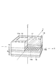
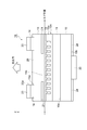
- FIG. 1 is a perspective view showing a configuration of a semiconductor light emitting device as a light emitting device according to a first embodiment of the present invention.
- FIG. I a plan view of the phase modulation layer. These are figures which show the positional relationship of the different refractive index area
- FIG. 11A is a diagram showing a phase distribution corresponding to the beam pattern shown in FIG. 11A
- FIG. 12B is a partially enlarged view of FIG.
- the figures which show notionally the example of the beam pattern of the traveling wave of each direction.
- the inclination angle of the straight line D with respect to the X axis and the Y axis is 45 °.
- FIG. 1 These are figures which show a mode that the traveling wave which travels in the surface of a phase modulation layer is scattered or reflected.
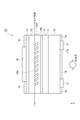
- FIG. 1 These are figures which show the cross-section of a semiconductor light-emitting device as a light-emitting device based on 2nd Embodiment. These are figures which show the case where a phase modulation layer is provided between the clad layer 11 and the active layer 12.
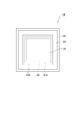
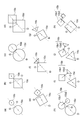
- FIG. 1 These are the top views which looked at the semiconductor light emitting element from the surface side. These are top views which show the example of the shape in XY plane of a different refractive index area
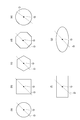
- top views which show the example of the shape in XY plane of a different refractive index area
- top views which show another example of the shape of the modified refractive index area
- top views which show another example of the shape of the modified refractive index area
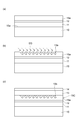
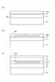
- region These are figures which show typically the cross-section of a semiconductor light-emitting device as a 3rd modification. These are figures for demonstrating the manufacturing method of the phase modulation layer of a 3rd modification.
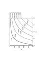
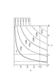
- sectional drawing and refractive index distribution which show three-layer slab structure regarding an optical waveguide layer in six-layer slab type
- the light emitting device is a light emitting device that outputs light for forming an optical image in at least one of the normal direction of the main surface and the inclined direction inclined with respect to the normal direction. And a structure for reducing one of the primary light and the ⁇ 1st light with respect to the other light. That is, as one embodiment, the light emitting device includes a substrate having a main surface, a light emitting portion provided on the substrate, and a phase modulation layer provided on the substrate in a state optically coupled to the light emitting portion. And.
- the phase modulation layer includes a base layer and a plurality of different refractive index regions having a refractive index different from the refractive index of the base layer. On the design surface of the phase modulation layer orthogonal to the normal direction, the plurality of different refractive index regions are arranged at predetermined positions in the base layer in accordance with the arrangement pattern for forming an optical image.
- each of the plurality of different refractive index regions is a first surface facing the main surface, a second surface located on the opposite side to the main surface with respect to the first surface, and It has a three-dimensional shape defined by a side connecting one side and the second side.
- at least one of the first surface, the second surface, and the side surface includes a portion inclined with respect to the main surface.
- the inclined portion may be the entire target surface or may be a partial region.
- portion inclined to the main surface In the “portion inclined to the main surface (entire surface or part of the surface)”, the main surface or a portion orthogonal to the normal direction, and the main surface and the normal direction of the main surface None of the parallel parts are included. In other words, when based on the main surface, both the portion parallel to the main surface and the portion perpendicular to the main surface are excluded from the “portion inclined to the main surface”.
- the surface parallel to the main surface (The light traveling in the phase modulation layer along the traveling surface) is scattered or reflected in the direction crossing the traveling surface at at least a part of the interface.
- two light beams (first-order light and -1st-order light) traveling in opposite directions on the traveling surface have a difference in the magnitude of scattering in different directions, or they differ in different directions. A difference occurs in the magnitude of the reflection.
- the primary light (or ⁇ 1st light) is strongly scattered (or reflected) toward the substrate, and the ⁇ 1st light (or primary light) is strongly scattered (or reflected) to the side opposite to the substrate Be done.
- the light path until the light is output to the outside of the apparatus is different between the light containing the primary light as the main component and the light containing the ⁇ 1st light as the main component, so the light with the longer light path has the shorter light path Attenuates more compared to the light of Therefore, according to the light emitting device, one of the primary light and the ⁇ 1st light can be attenuated with respect to the other light.
- phase modulation method determination method of the position of the different refractive index area
- phase modulation amount shift amount of the different refractive index area
- each of the plurality of different refractive index regions includes the base layer and one or more layers (for example, a clad layer, an active layer, etc.) in contact with the base layer. It may be an enclosed space defined by An inert gas such as argon, nitrogen, hydrogen or air may be enclosed in the enclosed space to be the different refractive index region.
- each of the plurality of different refractive index regions is a plane in which the width along the first direction on the design surface gradually decreases along the second direction intersecting the first direction. It is preferred to have a shape.
- the interface between the semiconductor layer and the different refractive index region is inclined with respect to the main surface of the substrate. Therefore, it is possible to easily realize a configuration in which at least a part of the interface between the plurality of different refractive index regions and the layer therearound is inclined with respect to the main surface.
- at least a portion of the first surface may be inclined with respect to the second surface.
- the side surface may include a portion (inclined portion) inclined with respect to the main surface.
- the main surface of the substrate is similar to the structure described in Patent Document 1 (structure in which the center of gravity of each different refractive index area has a rotation angle according to the light image around each lattice point)
- the light which forms the light image of arbitrary shapes may be output in the inclination direction inclined with respect to the normal direction of.
- each of the plurality of different refractive index regions corresponds one to one to any lattice point of the virtual square lattice. , Will be placed. However, it is not necessary to assign corresponding refractive index regions to all lattice points. Therefore, in the present specification, a lattice point to which one of the different refractive index regions is associated among lattice points constituting a virtual square lattice is referred to as an “effective lattice point”.
- a line connecting any specific grid point and the center of gravity of the specific heterorefractive index region associated with the specific grid point is the shortest distance to the specific grid point. It is preferable to be parallel to each of the line segments connecting the plurality of adjacent peripheral grid points and the centers of gravity of the plurality of peripheral different refractive index areas respectively associated with the plurality of peripheral grid points.
- a line segment connecting an arbitrary specific lattice point and the center of the specific modified refractive index area corresponding to the specific lattice point at a plurality of effective lattice points is a specific lattice point It may be parallel to each of the line segments connecting the remaining effective lattice points excluding ⁇ and the remaining different refractive index areas respectively associated with the remaining effective lattice points. In this case, the barycentric arrangement of each of the different refractive index regions can be easily designed.
- the inclination angle (an angle formed by any one of line segments starting from a grid point that is parallel to the square grid and the straight line passing through the grid point) is 0 °, 90 °, 180 ° and 270 °. It may be an angle other than. Furthermore, the inclination angle may be 45 °, 135 °, 225 ° or 315 °.
- the inclination angle when the inclination angle is 0 ° or 180 ° and the straight line is along the X axis, two traveling waves facing each other in the Y axis direction among the four fundamental waves do not receive phase modulation, and thus do not contribute to signal light. Further, when the inclination angle is 90 ° or 270 ° and the straight line is along the Y axis, two traveling waves opposed in the X axis direction do not contribute to the signal light. Therefore, when the inclination angle is 0 °, 90 °, 180 °, or 270 °, the generation efficiency of the signal light is lowered.
- the light emitting unit is preferably an active layer provided on a substrate.
- the light emitting portion and the phase modulation layer can be easily optically coupled.
- the method of manufacturing a light emitting device manufactures a light emitting device having the above-described structure.
- the manufacturing method includes, in the first step of providing a base layer on a substrate, and a plurality of holes or recesses that are to be a plurality of different refractive index regions by dry etching. And forming a second step.
- dry etching applies an etching reaction gas to the base layer from a direction inclined with respect to the normal direction of the main surface of the substrate.
- the side surfaces of the plurality of holes or recesses are inclined with respect to the normal direction of the main surface of the substrate. Therefore, a configuration can be easily realized in which at least a part of the interface between the plurality of different refractive index regions and the layer therearound is inclined with respect to the main surface or the normal direction of the main surface.
- the manufacturing method of the light-emitting device which concerns on this embodiment WHEREIN: The 1st process of providing a basic layer on a board
- the source gas for forming the lid layer is preferably applied to the base layer from a direction inclined with respect to the normal direction of the main surface of the substrate.
- the surface of the lid layer covering the opening portions of the plurality of holes or recesses inclines with respect to the main surface of the substrate in the third step, the surface of the lid layer covering the opening portions of the plurality of holes or recesses inclines with respect to the main surface of the substrate. Therefore, a configuration in which at least a part of the interface between the plurality of different refractive index regions and the layer therearound is inclined with respect to the main surface or the normal direction of the main surface can be easily realized.
- the direction in which the etching reaction gas for forming the plurality of holes or recesses may be supplied may be different from the direction in which the source gas is supplied.
- each aspect listed in the column of [Description of the embodiment of the present invention] is applicable to each of all the remaining aspects or to all combinations of these remaining aspects. .
- FIG. 1 is a perspective view showing a configuration of a semiconductor light emitting element 1A as a light emitting device according to a first embodiment of the present invention.
- An XYZ orthogonal coordinate system is defined in which an axis extending through the center of the semiconductor light emitting element 1A and extending in the thickness direction of the semiconductor light emitting element 1A is the Z axis.
- the semiconductor light emitting element 1A is an S-iPM laser that forms a standing wave along an XY plane and outputs a phase-controlled plane wave in the Z-axis direction, and as described later, the main element of the semiconductor substrate 10 A two-dimensional light image of an arbitrary shape is output in the direction perpendicular to the surface 10a (that is, the Z-axis direction) and / or the direction inclined thereto.
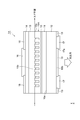
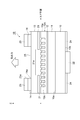
- FIG. 2 is a view schematically showing a laminated structure of the semiconductor light emitting element 1A.
- the semiconductor light emitting element 1A is provided on an active layer 12 as a light emitting portion provided on the main surface 10a of the semiconductor substrate 10 and an active layer 12 provided on the main surface 10a.
- a contact layer 14 provided on the cladding layer 13.
- the semiconductor substrate 10 and the layers 11 to 14 are made of a compound semiconductor such as a GaAs-based semiconductor, an InP-based semiconductor, or a nitride-based semiconductor.
- the energy band gap of the cladding layer 11 and the energy band gap of the cladding layer 13 are larger than the energy band gap of the active layer 12.
- the thickness direction of the semiconductor substrate 10 and the layers 11 to 14 coincides with the Z-axis direction.
- the light guide layer may include a carrier barrier layer for efficiently confining carriers in the active layer 12.
- the semiconductor light emitting device 1A further includes a phase modulation layer 15A optically coupled to the active layer 12.
- the phase modulation layer 15A is provided between the active layer 12 and the cladding layer 13.
- a light guide layer may be provided between the cladding layer 11 and the cladding layer 13 as needed.
- the thickness direction of the phase modulation layer 15A coincides with the Z-axis direction.
- phase modulation layer 15 ⁇ / b> A may be provided between the cladding layer 11 and the active layer 12.
- a light guide layer may be provided between the cladding layer 11 and the cladding layer 13 as needed.
- the phase modulation layer 15A includes a base layer 15a and a plurality of different refractive index areas 15b present in the base layer 15a.
- the base layer 15a is made of a first refractive index medium
- each of the plurality of different refractive index areas 15b is made of a second refractive index medium having a refractive index different from the refractive index of the first refractive index medium.
- the modified refractive index area 15b of the present embodiment is defined by a recess provided in the base layer 15a. In the recess, an inert gas such as argon, nitrogen, hydrogen or air may be enclosed.
- the modified refractive index region 15b may be a hole provided in the base layer 15a.
- the phase modulation layer 15A can select the wavelength ⁇ 0 among the emission wavelengths of the active layer 12 and output it to the outside.
- the light input into the phase modulation layer 15A forms a predetermined mode in the phase modulation layer 15A according to the arrangement of the differential refractive index region 15b, and the back surface of the semiconductor light emitting element 1A is formed as a laser beam having a desired pattern. Output to the outside.
- Each modified refractive index region 15 b has a refractive index interface with the base layer 15 a and a refractive index interface with the cladding layer 13. Then, at least a portion of the refractive index interface between each modified refractive index region 15b and the layer therearound (at least a portion of the surface defining the three-dimensional shape of each modified refractive index region 15b) is the main surface 10a (XY) It is inclined with respect to the plane parallel to the plane) and the normal direction (Z-axis direction) of the major surface 10a.
- each modified refractive index region 15b constitute a refractive index interface with the base layer 15a.
- the upper surface of each modified refractive index region 15 b (the second surface located on the opposite side to the main surface 10 a with respect to the first surface) forms a refractive index interface with the cladding layer 13.
- the bottom surface of each modified refractive index region 15b is perpendicular to the thickness direction of the phase modulation layer 15A (parallel to the XY plane).
- the side surface of each modified refractive index area 15b is along the direction (Z-axis direction) perpendicular to the major surface 10a.
- each modified refractive index region 15b is a direction perpendicular to main surface 10a (parallel to the XY plane) and main surface 10a. It is inclined with respect to (Z-axis direction).
- the inclination directions of the upper surface are aligned with one another in the multiple refractive index regions 15 b.
- Such a shape of the upper surface is realized by a part of the cladding layer 13 getting into the recess of the modified refractive index area 15 b or a part of the modified refractive index area 15 b getting into the cladding layer 13.
- the semiconductor light emitting element 1A further includes an electrode 16 provided on the contact layer 14 and an electrode 17 provided on the back surface 10b of the semiconductor substrate 10.
- the electrode 16 is in ohmic contact with the contact layer 14, and the electrode 17 is in ohmic contact with the semiconductor substrate 10. Furthermore, the electrode 17 has an opening 17a.
- the electrode 16 is provided in the central region of the contact layer 14. The portion of the contact layer 14 other than the electrode 16 is covered by a protective film 18 (see FIG. 2). The contact layer 14 not in contact with the electrode 16 may be removed. A portion (including the inside of the opening 17 a) of the back surface 10 b of the semiconductor substrate 10 other than the electrode 17 is covered with the anti-reflection film 19. The antireflective film 19 in the area other than the opening 17a may be removed.
- the light output from the active layer 12 enters the inside of the phase modulation layer 15A, and forms a predetermined mode according to the lattice structure formed in the phase modulation layer 15A.
- the laser light output from the phase modulation layer 15A is directly output from the back surface 10b through the opening 17a to the outside of the semiconductor light emitting element 1A or after being reflected by the electrode 16, the opening is made from the back surface 10b.
- the light is output to the outside of the semiconductor light emitting element 1A through 17a. At this time, zero-order light included in the laser light is output in a direction (normal direction) perpendicular to the major surface 10 a.
- signal light (primary light and -1 order light) included in the laser light is output in a two-dimensional arbitrary direction including a direction perpendicular to the major surface 10a and a direction inclined with respect thereto. . It is the signal light that forms the desired light image.
- the semiconductor substrate 10 is a GaAs substrate, and the cladding layer 11, the active layer 12, the cladding layer 13, the contact layer 14, and the phase modulation layer 15A are compound semiconductor layers composed of group III elements and group V elements, respectively.
- the cladding layer 11 is made of AlGaAs.
- the active layer 12 has a multiple quantum well structure (barrier layer: AlGaAs / well layer: InGaAs).
- the basic layer 15a is made of GaAs
- the modified refractive index area 15b is a recess or a hole.
- the cladding layer 13 is made of AlGaAs
- the contact layer 14 is made of GaAs.
- the energy band gap and the refractive index can be easily changed by changing the composition ratio of Al.
- Al x Ga 1 -x As when the composition ratio x of Al having a relatively small atomic radius is decreased (increased), the energy band gap positively correlated with this decreases (large).
- In when In is introduced by mixing In with a large atomic radius into GaAs, the energy band gap decreases. That is, the Al composition ratio of the cladding layers 11 and 13 is larger than the Al composition ratio of the barrier layer (AlGaAs) of the active layer 12.
- the Al composition ratio of the cladding layers 11 and 13 is set to, for example, 0.2 to 1.0 (for example, 0.4).
- the Al composition ratio of the barrier layer of the active layer 12 is set to, for example, 0 to 0.3 (for example, 0.15).
- noise light having a mesh-like dark portion may be superimposed on a beam pattern corresponding to an optical image output from the semiconductor light emitting element 1A.
- the noise light having the mesh-like dark part is caused by the higher order mode in the stacking direction inside the semiconductor light emitting element 1A.
- the fundamental mode in the stacking direction means a mode having an intensity distribution in which one peak exists over the region including the active layer 12 and sandwiched between the cladding layer 11 and the cladding layer 13.
- the higher order mode means a mode having an intensity distribution in which two or more peaks are present.
- the peak of the intensity distribution of the fundamental mode is formed in the vicinity of the active layer 12, while the peak of the intensity distribution of the higher mode is also formed in the cladding layer 11, the cladding layer 13, the contact layer 14 and the like. Further, as modes in the stacking direction, guided modes and leak modes exist, but leak modes do not exist stably. Therefore, in the following description, only the guided mode is focused. Further, in the guided mode, there are TE mode in which the electric field vector exists in the direction along the XY plane, and TM mode in which the electric field vector exists in the direction perpendicular to the XY plane. Focus on the mode only.
- the refractive index of the cladding layer 13 between the active layer 12 and the contact layer is larger than the refractive index of the cladding layer 11 between the active layer 12 and the semiconductor substrate, the higher order mode as described above is remarkable. It occurs.
- the refractive indices of the active layer 12 and the contact layer 14 are much larger than the refractive indices of the cladding layers 11 and 13. Therefore, when the refractive index of the cladding layer 13 is larger than the refractive index of the cladding layer 11, light is confined also in the cladding layer 13 to form a waveguide mode. This results in higher order modes.
- the refractive index of the cladding layer 13 is equal to or less than the refractive index of the cladding layer 11.
- the optical waveguide layer including the active layer 12 will be described.
- the optical waveguide layer includes only the active layer 12 (the optical waveguide layer includes the cladding layer 11, the cladding layer 13, and the phase modulation layer 15A is not included), it is regarded as a three-layer slab waveguide structure comprising such an optical waveguide layer and upper and lower two layers adjacent to the optical waveguide layer.
- the optical waveguide layer includes the phase modulation layer 15A and the active layer 12 (cladding layer 11 and cladding layer 13 are not included) It is regarded as a three-layer slab waveguide structure including such an optical waveguide layer and two upper and lower layers adjacent to the optical waveguide layer.
- the guided mode in the layer thickness direction is the TE mode.
- the normalized propagation constant b of standards influencing for good waveguide width V 1 and TE mode of the optical waveguide layer is defined by the following equation (1).
- the equivalent refractive index of TE mode is a cladding layer so that the waveguide mode does not leak to the semiconductor substrate 10 through the cladding layer 11.
- the refractive index of 11 needs to be higher, and the normalized propagation constant b needs to satisfy the following equation (2).
- a ′ and b each represent an asymmetry parameter and a normalized propagation constant in the three-layer slab waveguide, and are real numbers satisfying the following equations (3) and (4), respectively.
- n clad is the refractive index of the cladding layer 11
- n 1 is the refractive index of the optical waveguide layer including the active layer 12
- n 2 is the layer adjacent to the optical waveguide layer.
- refractive index of the high refractive index layer n 3 is the refractive index of the low layer of the refractive index of the layer adjacent to the optical waveguide layer
- n eff is the two layers of upper and lower adjacent to the optical waveguide layer and the optical waveguide layer It is an equivalent refractive index of TE mode with respect to 3 layer slab waveguide structure.
- the inventors According to the research of the inventors, it has been found that high-order modes are generated also in the optical waveguide layer (high refractive index layer) including the active layer 12. Then, the inventors have found that higher order modes can be suppressed by appropriately controlling the thickness and refractive index of the optical waveguide layer. That is, the value of the standard influencing for good waveguide width V 1 of the optical waveguide layer satisfies the condition described above, generation of higher order modes is further suppressed, and more of the noise light having a net-like dark portion that is superimposed on the beam pattern Further reduction is possible.
- the preferred thickness of the contact layer 14 is as follows. That is, in the three-layer slab waveguide structure including the contact layer 14 and the two upper and lower layers adjacent to the contact layer 14, the normalized waveguide width V 2 and the normalized propagation constant b of the TE mode are expressed by Defined by). However, when the guided mode is formed in the contact layer (the mode order is N 2 ), the equivalent refractive index of the TE mode is the clad layer 11 so that the guided mode does not leak to the semiconductor substrate 10 through the clad layer 11.
- the normalized propagation constant b needs to satisfy the following equation (6). At this time, as long as it is within the range of No that the equation (5) and (6) Standard influencing for good waveguide width V 2 collapsed meet, mode guided through the contact layer 14 is even not exist fundamental mode.
- a ′ and b respectively represent an asymmetry parameter and a normalized propagation constant in the three-layer slab waveguide, and are real numbers satisfying the following equations (7) and (8), respectively.
- n 4 is the refractive index of the contact layer 14
- n 5 is the refractive index of the layer having a high refractive index among the layers adjacent to the contact layer 14
- n 6 is the contact layer Among the layers adjacent to S.14 , the refractive index of the layer having a low refractive index among the adjacent layers
- n eff is the equivalent refractive index of the TE mode with respect to the contact layer 14 and the adjacent three-layer slab waveguide structure of upper and lower two layers.
- the generation of the guided mode caused by the contact layer 14 can be suppressed, and the generation of the higher order mode generated in the semiconductor light emitting device can be further suppressed.
- the semiconductor substrate 10 is an InP substrate, and the cladding layer 11, the active layer 12, the phase modulation layer 15A, the cladding layer 13, and the contact layer 14 are made of, for example, an InP-based compound semiconductor.
- the cladding layer 11 is made of InP.
- the active layer 12 has a multiple quantum well structure (barrier layer: GaInAsP / well layer: GaInAsP).
- the basic layer 15a is made of GaInAsP
- the modified refractive index area 15b is a recess (may be a void).
- the cladding layer 13 is made of InP.
- the contact layer 14 is made of GaInAsP.
- the semiconductor substrate 10 is a GaN substrate
- the cladding layer 11, the active layer 12, the phase modulation layer 15A, the cladding layer 13, and the contact layer 14 are made of, for example, a nitride compound semiconductor.
- the cladding layer 11 is made of AlGaN.
- the active layer 12 has a multiple quantum well structure (barrier layer: InGaN / well layer: InGaN).
- the basic layer 15a is made of GaN
- the modified refractive index area 15b is a recess (may be a void).
- the cladding layer 13 is made of AlGaN.
- the contact layer 14 is made of GaN.
- the same conductivity type as the semiconductor substrate 10 is given to the cladding layer 11, and the opposite conductivity type to the semiconductor substrate 10 is given to the cladding layer 13 and the contact layer 14.
- the semiconductor substrate 10 and the cladding layer 11 are n-type, and the cladding layer 13 and the contact layer 14 are p-type.
- the phase modulation layer 15A has the same conductivity type as the semiconductor substrate 10.
- the phase modulation layer 15A is provided between the active layer 12 and the cladding layer 13, the phase modulation layer 15A has a conductivity type opposite to that of the semiconductor substrate 10.
- the impurity concentration is, for example, 1 ⁇ 10 17 to 1 ⁇ 10 21 / cm 3 .
- the active layer 12 is intrinsic (i-type) to which no impurity is intentionally added, and the impurity concentration is 1 ⁇ 10 15 / cm 3 or less. Further, the impurity concentration of the phase modulation layer 15A may be intrinsic (i-type), for example, when it is necessary to suppress the influence of loss due to light absorption through the impurity level.
- the thickness of the semiconductor substrate 10 is, for example, 150 ⁇ m.
- the thickness of the cladding layer 11 is, for example, 2000 nm.
- the thickness of the active layer 12 is, for example, 175 nm.
- the thickness of the phase modulation layer 15A is, for example, 280 nm.
- the depth of the modified refractive index area 15b is, for example, 200 nm.
- the thickness of the cladding layer 13 is, for example, 2000 nm.
- the thickness of the contact layer 14 is, for example, 150 nm.
- the antireflective film 19 is made of, for example, a dielectric single layer film such as silicon nitride (for example, SiN), silicon oxide (for example, SiO 2 ) or the like, or a dielectric multilayer film.
- dielectric multilayer films include titanium oxide (TiO 2 ), silicon dioxide (SiO 2 ), silicon monoxide (SiO), niobium oxide (Nb 2 O 5 ), tantalum pentoxide (Ta 2 O 5 ), and fluorine.
- Dielectric layers such as magnesium fluoride (MgF 2 ), titanium oxide (TiO 2 ), aluminum oxide (Al 2 O 3 ), cerium oxide (CeO 2 ), indium oxide (In 2 O 3 ), zirconium oxide (ZrO 2 )
- MgF 2 magnesium fluoride
- TiO 2 titanium oxide
- Al 2 O 3 aluminum oxide
- CeO 2 cerium oxide
- In 2 O 3 indium oxide
- a film in which two or more types of dielectric layers selected from the group are stacked can be used.
- a film with a thickness of ⁇ / 4 is stacked with an optical film thickness for light of wavelength ⁇ .
- the protective film 18 is, for example, an insulating film such as silicon nitride (for example, SiN) or silicon oxide (for example, SiO 2 ).
- the electrode 16 can be made of a material containing at least one of Cr, Ti, and Pt, and Au, for example, a Cr layer and an Au layer.
- the electrode 17 can be made of a material containing at least one of AuGe and Ni, and Au, and has, for example, a laminated structure of an AuGe layer and an Au layer.
- the materials of the electrodes 16 and 17 are not limited to these ranges as long as ohmic contact can be realized.
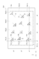
- FIG. 4 is a plan view of the phase modulation layer 15A.
- the phase modulation layer 15A includes the base layer 15a and the modified refractive index area 15b.
- the base layer 15a is made of a first refractive index medium
- the modified refractive index area 15b is made of a second refractive index medium having a refractive index different from that of the first refractive index medium.
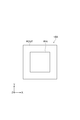
- a virtual square lattice is set on the design surface of the phase modulation layer 15A that coincides with the XY plane. One side of the square lattice is parallel to the X axis, and the other side is parallel to the Y axis.
- a square unit configuration region R centered on the lattice point O of the square lattice can be set in a two-dimensional manner over a plurality of columns along the X axis and a plurality of rows along the Y axis.
- a square unit configuration region R centered on the lattice point O of the square lattice is arranged in parallel along a plurality of columns (x1 to x4) arranged in parallel along the X axis and the Y axis.
- a plurality of lines (y1 to y3) are set in a two-dimensional manner.
- the modified refractive index areas 15 b are provided one by one in each unit configuration area R.
- the lattice point O may be located outside the modified refractive index area 15 b or may be included inside the modified refractive index area 15 b.
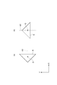
- the planar shape of each of the plurality of modified refractive index regions 15b is a shape in which the width in a certain direction on the XY plane gradually narrows along the direction intersecting the direction.
- FIG. 4 shows a triangular shape as an example of such a shape. That is, it has a shape in which the width gradually narrows from a certain side toward the vertex facing the side. This triangle is, for example, an isosceles triangle. As shown in FIGS.
- the refractive index interface defined by the modified refractive index region 15 b and at least one of the cladding layer 11 and the active layer 12 has a principal surface 10 a (X ⁇ It is inclined with respect to a direction (Z-axis direction) perpendicular to the Y plane) and the major surface 10a.
- the inclination direction coincides with the direction from a certain side to the vertex opposite to the side.
- the directions are aligned with one another in the plurality of different refractive index regions 15b. In one example, the angle between this direction and the X-axis direction is 45 ° or 135 °.
- the ratio of the area SA of the differential refractive index area 15b occupied in one unit constituent area R is referred to as a filling factor (FF).
- FF filling factor
- SA is the area of the modified refractive index area 15b in the XY plane.
- LA LA ⁇ h / 2.
- the lattice spacing a of the square lattice is about the wavelength divided by the equivalent refractive index, and is set to, for example, about 300 nm.
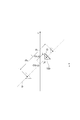
- FIG. 5 is a view showing the positional relationship of the modified refractive index area 15b in the phase modulation layer 15A.
- the center of gravity G of each modified refractive index area 15 b is disposed on the straight line D.
- the straight line D is a straight line that passes through the corresponding grid point O (x, y) of the unit constituent region R (x, y) and is inclined with respect to each side of the square lattice.
- the straight line D is a straight line inclined with respect to both the s axis (parallel to the X axis) and the t axis (parallel to the Y axis) defining the unit constituent region R (x, y).
- the inclination angle of the straight line D with respect to the s axis (inclination angle based on a part of the s axis starting from the lattice point) is ⁇ .
- the inclination angle ⁇ is constant in the phase modulation layer 15A (a part of the phase modulation layer 15A may be constant).
- the straight line D extends from the first quadrant to the third quadrant of the coordinate plane defined by the s-axis and t-axis. .
- the straight line D extends from the second quadrant to the fourth quadrant of the coordinate plane defined by the s-axis and t-axis. .
- the inclination angle ⁇ is an angle excluding 0 °, 90 °, 180 ° and 270 °.
- the distance between the grid point O (x, y) and the center of gravity G is r (x, y).
- x indicates the position of the x-th grid point on the X axis
- y indicates the position of the y-th grid point on the Y axis.
- the center of gravity G is located in the first quadrant (or the second quadrant).
- the distance r (x, y) is a negative value
- the center of gravity G is located in the third quadrant (or the fourth quadrant).
- the distance r (x, y) is zero, the grid point O and the center of gravity G coincide with each other.
- the different refractive index areas 15b are individually set according to the beam pattern (light image). That is, the distribution of the distance r (x, y) has a specific value at each position determined by the values of x (x1 to x4 in the example of FIG. 4) and y (y1 to y3 in the example of FIG. 4). It is not necessarily represented by a specific function.
- the distribution of the distance r (x, y) is determined from the complex amplitude distribution obtained by inverse Fourier transform of the output beam pattern from which the phase distribution is extracted. That is, when the phase P (x, y) in the unit constituent region R (x, y) is P 0 described later, the distance r (x, y) is set to 0, and the phase P (x, y) distance r (x, y) is set to the maximum value R 0 is when There is a ⁇ + P 0, when the phase P (x, y) is a - [pi] + P 0 is distance r (x, y) is the minimum value -R Set to 0 .
- the initial phase P 0 can be set arbitrarily.
- the maximum value R 0 of r (x, y) is, for example, within the range of the following formula (9). Note that when finding the complex amplitude distribution from the output beam pattern, the reproducibility of the beam pattern is improved by applying an iterative algorithm such as the Gerchberg-Saxton (GS) method that is generally used when calculating the hologram generation. Do.
- FIG. 6 is a plan view showing an example in which the substantially periodic refractive index structure of FIG. 4 is applied only in a specific region of the phase modulation layer.
- a substantially periodic structure for outputting a desired beam pattern is formed inside the square inner region RIN.
- the outer region ROUT surrounding the inner region RIN a circular different refractive index region having a coincident barycentric position is disposed at the grid point position of the square lattice.
- light is also distributed in the outer region ROUT to suppress generation of high frequency noise (so-called window function noise) caused by a sudden change in light intensity in the peripheral portion of the inner region RIN. it can.
- window function noise high frequency noise
- light leakage in a direction parallel to the XY plane can be suppressed, and reduction in threshold current can be expected.
- FIG. 7 is a diagram for explaining the relationship between the output beam pattern (optical image) from the semiconductor light emitting element 1A and the distribution of distances in the phase modulation layer 15A.
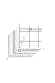
- a Kx-Ky plane obtained by converting a beam projection area, which is a projection area of an output beam pattern, onto a wave number space.
- the Kx-axis and the Ky-axis defining the Kx-Ky plane are orthogonal to each other, and each projects the projection direction of the output beam pattern from the normal direction (Z-axis direction) of the main surface 10a to the in-plane of the main surface 10a. It corresponds to an angle with respect to the normal direction when it is shaken in the direction (details will be described later).
- a specific region including an output beam pattern is constituted by M2 (an integer of 1 or more) ⁇ N2 (an integer of 1 or more) square image regions FR.
- a virtual square lattice set on the design surface (X-Y plane) of the phase modulation layer 15A is configured by M1 (an integer of 1 or more) ⁇ N1 (an integer of 1 or more) unit configuration regions R Shall be
- M2 does not have to match the integer M1.
- the integer N2 does not have to match the integer N1.
- the image region FR (k x , k y ) in each is specified by the coordinate component x (an integer of 1 or more and M1 or less) in the X axis direction and the coordinate component y (an integer of 1 or more and N1 or less) in the Y axis direction
- the complex amplitude F (x, y) in the unit constituent region R (x, y) subjected to the two-dimensional inverse Fourier transform to the unit constituent region R (x, y) is the amplitude term A (x, y) and the phase term P (P It is defined by x, y).
- the amplitude term A in the complex amplitude F (x, y) of the unit constituent region R (x, y) corresponds to the amplitude distribution on the XY plane.
- the distribution of the phase term P (x, y) in the complex amplitude F (x, y) of the unit constituent region R (x, y) is X ⁇ It corresponds to the phase distribution on the Y plane.
- the distribution of the distance r (x, y) of (x, y) corresponds to the distance distribution on the XY plane.
- FIG. 7 shows four quadrants whose origin is the center Q. .
- FIG. 7 shows the case where light images are obtained in the first and third quadrants as an example, it is also possible to obtain images in the second and fourth quadrants or all quadrants.
- a pattern symmetrical with respect to the origin is obtained.
- FIG. 7 shows, as an example, a case where a pattern obtained by rotating the letter "A" in the third quadrant and the letter "A" in the first quadrant by 180 ° is obtained.
- a rotationally symmetric light image for example, a cross, a circle, a double circle, etc.
- the light images are superimposed and observed as one light image.
- the output beam pattern (optical image) of the semiconductor light emitting element 1A is at least one of a spot, a spot group consisting of three or more points, a straight line, a cross, a line drawing, a lattice pattern, a photograph, a stripe pattern, CG (computer graphics) and characters.
- the light image corresponds to the designed light image (original image) represented by one.
- the distribution of the distance r (x, y) of the modified refractive index area 15b of the phase modulation layer 15A is determined by the following procedure.
- FIG. 8 is a diagram for explaining coordinate conversion from spherical coordinates (d1, ⁇ tilt , ⁇ rot ) to coordinates ( ⁇ , ⁇ , ⁇ ) in the XYZ orthogonal coordinate system, and the coordinates ( ⁇ , ,, By ⁇ ), a designed light image on a predetermined plane set in the XYZ rectangular coordinate system which is a real space is expressed.
- the angle theta tilt and theta rot has the following formula (13)
- the coordinate value k x on the Kx axis corresponding to the X axis, and the normalized wave number defined by the following equation (14) corresponding to the Y axis and along the Kx axis shall be converted into coordinate values k y on Ky axis orthogonal.
- the normalized wave number means the wave number normalized with the wave number corresponding to the lattice spacing of a virtual square lattice being 1.0.
- a specific wave number range including a beam pattern corresponding to an optical image is square M2 (integer of 1 or more) .times.N2 (integer of 1 or more) And the image region FR.
- the integer M2 does not have to match the integer M1.
- the integer N2 does not have to match the integer N1.
- Formula (13) and Formula (14) are described in the following document (1), for example.
- the corresponding different refractive index regions 15 b are disposed in the unit constituent region R (x, y) so as to satisfy the following relationship.
- the distance r (x, y) is set to 0 when the phase P (x, y) at a certain coordinate (x, y) is P 0 , and the phase P (x, y) is ⁇ + P 0
- the maximum value R 0 is set
- the minimum value ⁇ R 0 is set.
- the light image is subjected to inverse Fourier transform, and the distribution of the distance r (x, y) according to the phase P (x, y) of its complex amplitude is divided into a plurality of different refractive index regions Give it to 15b.
- the phase P (x, y) and the distance r (x, y) may be proportional to one another.
- the far-field pattern after Fourier transform of the laser beam has various shapes such as single or plural spot shapes, annular shapes, linear shapes, character shapes, double annular shapes, or Laguerre-Gaussian beam shapes. It can be taken. Since the beam direction can also be controlled, it is possible to realize, for example, a laser processing machine that electrically performs high-speed scanning by arraying the semiconductor light emitting elements 1A in one or two dimensions. Since the beam pattern is represented by angle information in the far field, if the target beam pattern is a bitmap image or the like represented by two-dimensional position information, it is once converted into angle information. Then, it is preferable to perform inverse Fourier transform after converting to wave number space.
- the amplitude distribution A (x, y) is calculated by using the abs function of the numerical analysis software "MATLAB" of The MathWorks.
- the phase distribution P (x, y) can be calculated by using MATLAB's angle function.
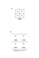
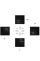
- FIG. 9B An output beam pattern calculated from the complex amplitude distribution obtained by the inverse Fourier transform of FIG. 9A, which is a desired light image, is as shown in FIG. 9B.
- the first quadrant of the output beam pattern shown in FIG. 9B is divided into four quadrants A1, A2, A3, and A4.
- the first quadrant of the original optical image is in the third quadrant of the obtained beam pattern.
- a pattern obtained by rotating the first quadrant of the original light image by 180 degrees appears in the first quadrant of the obtained beam pattern.
- the material system, the film thickness, and the layer structure may be variously changed.
- a scaling law holds. That is, when the wavelength is multiplied by a constant ⁇ , a similar standing wave state can be obtained by multiplying the entire square lattice structure by ⁇ .
- each compound semiconductor layer is formed by metal organic chemical vapor deposition (MOCVD) or molecular beam epitaxy (MBE).
- MOCVD metal organic chemical vapor deposition
- MBE molecular beam epitaxy
- the growth temperature of AlGaAs can be set to 500 ° C. to 850 ° C.
- TMA trimethylaluminum
- TMG trimethylgallium
- TEG triethylgallium
- AsH 3 arsine
- Si 2 H 6 source material for N-type impurities DEZn (diethyl zinc) is used as a raw material for disilane
- P-type impurities is used as a raw material for disilane.
- In the growth of GaAs TMG and arsine are used, but TMA is not used.
- InGaAs is manufactured using TMG, TMI (trimethylindium) and arsine.
- the insulating film is formed by sputtering a target using the constituent material as a raw material or by PCVD (plasma CVD).
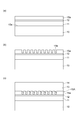
- FIG. 10A are diagrams showing steps in the method of manufacturing the semiconductor light emitting device 1A.
- the cladding layer 11, the active layer 12, and the base layer 15a are formed on the major surface 10a of the semiconductor substrate 10 by, for example, MOCVD (metal organic chemical vapor deposition) method. It is sequentially provided by the used epitaxial growth method.
- MOCVD metal organic chemical vapor deposition
- a two-dimensional fine pattern is drawn on the resist by an electron beam drawing apparatus.
- a two-dimensional fine pattern is formed on the resist by developing the resist on which the pattern is drawn.
- the two-dimensional fine pattern is transferred to the basic layer 15a by dry etching.
- a plurality of recesses may be formed to become the modified refractive index regions 15b.
- the planar shape of the plurality of recesses is, as described above, a shape in which the width in a certain direction gradually narrows along the direction crossing the direction (for example, a triangular shape, see FIG. 4).
- a step of forming a SiN layer or SiO 2 layer on the base layer 15a by PCVD before forming the resist a step of forming a resist mask on the formed layers (SiN layer or SiO 2 layer)
- the step of transferring the fine pattern to the SiN layer or the SiO 2 layer by reactive ion etching (RIE), and the step of performing dry etching after removing the resist may be sequentially performed. In this case, the resistance of dry etching can be enhanced.
- the cladding layer 13 and the contact layer 14 are sequentially provided by the MOCVD method.
- the cladding layer 13 is grown, the plurality of recesses as the modified refractive index regions 15 b are closed by the cladding layer 13.
- the degree of the entry changes in the recess due to the planar shape of the recess. That is, the degree of penetration of the cladding layer 13 changes between the wide portion of the recess and the narrow portion of the recess.
- the refractive index interface between the cladding layer 13 and the modified refractive index region 15 b is inclined with respect to the interface between the base layer 15 a and the cladding layer 13. Since the interface between the basic layer 15a and the cladding layer 13 is parallel to the major surface 10a, the refractive index interface between the cladding layer 13 and the modified refractive index region 15b is in the direction perpendicular to the major surface 10a and the major surface 10a. Will be inclined.
- FIG. 10C shows an example in which a part of the cladding layer 13 enters the recess, the recess may enter the cladding layer 13 in reverse. Such a method is described in the following document (2).
- Kazuyoshi Hirose et al. “Watt-class high-power, high-beam-quality photonic-crystal lasers”, Nature Phoronics 8, pp. 406-411 (2014)
- the electrodes 16 and 17 shown in FIG. 2 are formed by vapor deposition, sputtering or the like.
- the protective film 18 and the antireflective film 19 are formed by a sputtering method, a PCVD method, or the like, as necessary.
- the semiconductor light emitting element 1A of the present embodiment is manufactured through the above steps.
- the phase modulation layer 15A is provided between the active layer 12 and the cladding layer 11, the phase modulation layer 15A is formed on the cladding layer 11 before the formation of the active layer 12.
- the wave number k exists at the saddle point, but the size of the wave number vector is basically inverse If it is equal to the magnitude of the grating vector, a resonant mode (a standing wave in the XY plane) with a grating spacing a equal to the wavelength ⁇ is obtained. In the present embodiment, oscillation in such a resonance mode (standing wave state) is obtained.
- the standing wave in the phase modulation layer 15A described above is scattered by the different refractive index area 15b having a predetermined shape, and the wavefront obtained in the vertical direction (Z-axis direction) is phase-modulated.
- the desired beam pattern is obtained. For this reason, a desired beam pattern can be obtained without the polarizing plate.
- This beam pattern is not only a pair of single-peak beams (spots), but also, as described above, a character shape, two or more identical shape spot groups, or a vector whose phase and intensity distribution are spatially nonuniform. It is also possible to use a beam or the like.
- the refractive index of the basic layer 15a is preferably 3.0 to 3.5, and the refractive index of the modified refractive index region 15b is preferably 1.0 to 3.4.
- the average radius of the recess (different refractive index region 15b) of the basic layer 15a is, for example, 20 nm to 120 nm in the case of the 940 nm band.
- the diffraction efficiency is proportional to the light coupling coefficient ⁇ 1 represented by a first-order coefficient when Fourier transforming the shape of the modified refractive index area 15b.
- the light coupling coefficient is described, for example, in the following document (3).
- the phase modulation layer 15A optically coupled to the active layer 12 includes the base layer 15a and a plurality of different refractive index regions 15b having refractive indexes different from the refractive index of the base layer 15a. And.
- the lattice point O (x, y) including the lattice point O (x, y) of the virtual square lattice set on the design surface of the phase modulation layer 15A, the lattice point O (x, y) And a straight line D inclined with respect to each side of the square lattice (parallel to the s-axis and the t-axis defining the unit constituent region R (x, y)).
- the center of gravity G is arranged.
- the distance r (x, y) between the center of gravity G of the modified refractive index area 15 b and the corresponding lattice point O (x, y) is individually set for each lattice point according to the light image.
- the phase of the beam changes according to the distance between the lattice point O (x, y) and the center of gravity G. Therefore, only by changing the position of the center of gravity G, the phase of the beam output from each of the different refractive index areas 15b can be controlled, and the beam pattern formed as a whole can be controlled to a desired shape. Become.
- this semiconductor light emitting element 1A is an S-iPM laser, and according to such a structure, the center of gravity G of each modified refractive index area 15b is rotated according to the light image around each lattice point O (x, y) As in the conventional structure (rotation method) having an angle, the light forming an optical image of an arbitrary shape is output in the direction inclined with respect to the direction (normal direction) perpendicular to the major surface 10 a of the semiconductor substrate 10 be able to.
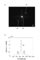
- FIG. 11A shows an example of a beam pattern (optical image) output from the semiconductor light emitting element 1A.
- the center of FIG. 11A corresponds to an axis that intersects the light emitting surface of the semiconductor light emitting element 1A and is perpendicular to the light emitting surface.
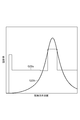
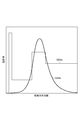
- FIG. 11B is a graph showing the light intensity distribution in a cross section including the axis. Fig.
- FIG. 11 (b) is a far-field image acquired using an FFP optical system (A3267-12 manufactured by Hamamatsu Photonics), a camera (ORCA-05G manufactured by Hamamatsu Photonics), and a beam profiler (Lepas-12 manufactured by Hamamatsu Photonics) It is the image which integrated
- the maximum count number in FIG. 11A is normalized at 255, and the central zero-order light B0 is saturated in order to clearly show the intensity ratio of ⁇ first-order light. From FIG. 11 (b), the difference in intensity between the primary light and the ⁇ 1st light can be easily understood.
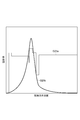
- FIG. 11 (b) is a far-field image acquired using an FFP optical system (A3267-12 manufactured by Hamamatsu Photonics), a camera (ORCA-05G manufactured by Hamamatsu Photonics), and a beam profiler (Lepas-12 manufactured by Hamamatsu Photonics) It is the
- FIGS. 12 (a) is a diagram showing a phase distribution corresponding to the beam pattern shown in FIG. 11 (a).
- FIG.12 (b) is the elements on larger scale of Fig.12 (a).
- the phase at each position in the phase modulation layer 15A is indicated by shading, and the darker part approaches the phase angle 0 °, and the bright part approaches the phase angle 360 °.
- the center value of the phase angle can be set arbitrarily, the phase angle may not necessarily be set within the range of 0 ° to 360 °.
- the semiconductor light emitting device 1A includes a primary light including a first light image portion B1 outputted in a first direction inclined with respect to the axis.
- the first light is output in a second direction that is symmetrical to the first direction with respect to the axis, and the first order light including the second light image portion B2 that is rotationally symmetrical with the first light image portion B1 with respect to the axis.
- the first light image portion B1 appears in the first quadrant in the XY plane
- the second light image portion B2 appears in the third quadrant in the XY plane.
- either primary light or negative primary light may not be required. In such a case, it is desirable to reduce unnecessary light of the primary light and the ⁇ 1st light with respect to the necessary light.
- FIG. 13 is a diagram conceptually showing an example of beam patterns of traveling waves in each direction.
- the inclination angle of the straight line D with respect to the s-axis and the t-axis is 45 °
- the maximum value R 0 of the distance r (x, y) to y) is set as in the following equation (17).
- fundamental traveling waves AU, AD, AR and AL are generated along the XY plane.
- the traveling waves AU and AD are lights traveling along one of the sides of the square lattice extending in the Y-axis direction.
- the traveling wave AU travels in the positive Y-axis direction
- the traveling wave AD travels in the negative Y-axis direction.
- the traveling waves AR and AL are light traveling along a side of the sides of the square lattice extending in the X-axis direction.
- the traveling wave AR travels in the positive X-axis direction
- the traveling wave AL travels in the negative X-axis direction. In this case, from the traveling waves traveling in opposite directions to each other, beam patterns in opposite directions can be obtained.
- a beam pattern BU including only the second light image portion B2 is obtained from the traveling wave AU, and a beam pattern BD including only the first light image portion B1 is obtained from the traveling wave AD.
- a beam pattern BR including only the second light image portion B2 is obtained from the traveling wave AR, and a beam pattern BL including only the first light image portion B1 is obtained from the traveling wave AL.
- one is primary light and the other is negative first-order light.
- phase modulation layer 15A of the present embodiment for a single traveling wave, a difference occurs in the light amount of each of the first-order light and the -1st-order light.
- the ideal phase distribution is obtained as the shift amount R 0 approaches the upper limit value of the above equation (9).
- the 0th-order light is reduced, and in each of the traveling waves AU, AD, AR, and AL, one of the 1st-order light and the -1st-order light is selectively reduced. Therefore, it is possible in principle to give a difference to the light amounts of the primary light and the ⁇ 1st light by selectively reducing any one of the traveling waves traveling in opposite directions.
- the method of the present embodiment in which the modified refractive index area 15b moves on the straight line D which passes through the lattice point O (x, y) and is inclined with respect to each side of the square lattice shown in FIG. The reason why it is possible to selectively reduce either the primary light or the ⁇ 1st light will be described.
- the design phase ⁇ (x, y) at a certain position the t axis (parallel to the Y axis) positive shown in FIGS. 12 (a) and 12 (b) as an example of four traveling waves.
- the traveling wave AU in the direction.
- the shift from the lattice point O is r ⁇ sin ⁇ ⁇ ⁇ (x, y) ⁇ 0 ⁇ / ⁇ , so the phase difference is The relation is 2 ⁇ / a) r ⁇ sin ⁇ ⁇ ⁇ (x, y) ⁇ 0 ⁇ / ⁇ .
- a function f (z) represented by the following equation (19) and satisfying the following equation (20) is expanded by Laurent series, a mathematical formula such as the following equation (21) holds.
- sinc (x) x / sin (x).
- the phase distribution ((x, y) can be subjected to series expansion, and the respective light quantities of the zeroth order light and the ⁇ first order lights can be described.
- the magnitude of the zero-order light component of the phase distribution ((x, y) is as follows, when it is noted that the absolute value of the exponent term exp ⁇ j ⁇ (c ⁇ n) ⁇ in the above equation (21) is 1.
- the magnitude of the primary light component is represented by the following formula (23)
- the magnitude of the ⁇ 1st order light component is represented by the following formula (24).
- zero-order light and minus first-order light components appear in addition to the first-order light component except under the condition defined by the following formula (25).
- the magnitudes of the ⁇ 1st-order light components are not equal to one another.
- the traveling wave AU in the t-axis direction (Y-axis positive direction) is considered as an example of the four traveling waves, but the same relationship applies to the other three waves (traveling waves AD, AR, AL) This holds true, and a difference occurs in the magnitude of ⁇ 1st-order light components.
- the interface between the modified refractive index region 15b and the upper layer (cladding layer 13 or active layer 12) is inclined with respect to the major surface 10a.
- the traveling waves AU, AD, AR, and AL traveling in the phase modulation layer 15A in parallel with the major surface 10a are phased at the interface between the differential refractive index region 15b and the upper layer thereof.
- the light is scattered or reflected in a direction (for example, the Z-axis direction) intersecting the design surface (the plane parallel to the XY plane) of the modulation layer 15A.
- two traveling waves AU and AD traveling in opposite directions along the major surface 10a in the phase modulation layer 15A are scattered or reflected in mutually different directions, and are separated from each other.
- two traveling waves AR and AL traveling in opposite directions in the plane of the phase modulation layer 15A are scattered or reflected in different directions, and are separated from each other.
- the traveling waves AU and AR which are primary light (or ⁇ 1st light) are scattered or reflected toward the semiconductor substrate 10, and the traveling waves AD and AL which are ⁇ 1st light (or 1st light) are semiconductors
- the light is scattered or reflected toward the side (electrode 16 side) opposite to the substrate 10. Therefore, the optical paths until the light is output to the outside of the device are different between the primary light and the ⁇ 1st light. Since the traveling waves AU and AR are scattered or reflected toward the semiconductor substrate 10, they pass through the semiconductor substrate 10 and are output to the outside as they are, and the optical path becomes short.
- the traveling waves AD and AL are scattered or reflected toward the opposite side to the semiconductor substrate 10, they are reflected by the electrode 16 and reach the semiconductor substrate 10 by an amount equal to that of the traveling waves AU and AR. Will be longer. Therefore, the traveling waves AD and AL are attenuated more than the traveling waves AU and AR due to the effects of light absorption in the semiconductor, incomplete reflection at the electrode 16, and scattering accompanying light propagation. Therefore, according to the semiconductor light emitting device 1A of the present embodiment, it is possible to reduce one of the primary light and the ⁇ 1st light with respect to the other light. Also in FIG. 11 (b) corresponding to the experimental result, it can be seen that there is a difference in intensity between the primary light and the ⁇ 1st light.
- the interface between the modified refractive index region 15b and the upper layer thereof is inclined with respect to the major surface 10a, but this is an example.
- the above-described effect can be suitably obtained by at least a part of the interface between the plurality of different refractive index areas 15b and the layer therearound being inclined with respect to the major surface 10a.
- the light emitting device including the semiconductor light emitting device 1A or the semiconductor light emitting device 1A attenuates one light.
- the light emitting device including the semiconductor light emitting device 1A or the semiconductor light emitting device 1A attenuates one light.
- a light absorbing layer provided between the phase modulation layer 15A and the semiconductor substrate 10 a light absorbing member provided outside the semiconductor light emitting element 1A, etc.
- one light may be output from the surface on the opposite side to the other light (that is, the surface on the side of the cladding layer 13 with respect to the active layer 12).
- the plurality of modified refractive index regions 15b are concave portions, and the planar shape of each of the plurality of modified refractive index regions 15b is gradually along the direction in which the width in one direction intersects the direction It may be narrow in shape.
- the interface between the semiconductor layer and the different refractive index region 15b is inclined with respect to the major surface 10a. Therefore, a configuration in which at least a part of the interface between the plurality of different refractive index regions 15 b and the layer therearound is inclined with respect to the major surface 10 a can be easily realized.
- the inclination angle ⁇ of the straight line D with respect to the square lattice may coincide at all lattice points set in the phase modulation layer 15A. This makes it possible to easily design the arrangement of the center of gravity G of the modified refractive index area 15b. Also, in this case, the inclination angle ⁇ may be 45 °, 135 °, 225 ° or 315 °. Thereby, two waves (for example, traveling waves AD, AR) orthogonal to each other traveling along the square lattice can equally contribute to the formation of a desired light image.
- traveling waves AD, AR orthogonal to each other traveling along the square lattice
- the inclination angle ⁇ is 0 °, 90 °, 180 ° or 270 °
- a pair of the progressions in the Y-axis direction or the X-axis direction out of the four traveling waves AU, AD, AR, and AL Since the wave does not contribute to the primary light (signal light), it is difficult to improve the efficiency of the signal light.
- the light emitting unit may be the active layer 12 provided on the semiconductor substrate 10. Thereby, the light emitting portion and the phase modulation layer 15A can be easily optically coupled.
- FIG. 15 is a view showing a cross-sectional structure of a semiconductor light emitting element 1B as a light emitting device according to the second embodiment.
- the semiconductor light emitting element 1B is a laser light source that forms a standing wave along the XY plane and outputs a phase controlled plane wave in the Z axis direction, and as in the first embodiment, the semiconductor substrate 10
- the light which forms a two-dimensional light image of an arbitrary shape is output in a direction including a direction (normal direction) perpendicular to the major surface 10a and an inclined direction inclined with respect to the normal direction.
- the semiconductor light emitting element 1A of the first embodiment outputs the beam pattern (optical image) transmitted through the semiconductor substrate 10 from the back surface
- the semiconductor light emitting element 1B of this embodiment has the cladding layer 13 with respect to the active layer 12.
- the beam pattern (light image) is output from the side surface.
- the semiconductor light emitting device 1B includes a cladding layer 11, an active layer 12, a cladding layer 13, a contact layer 14, a phase modulation layer 15A, and a current confinement layer 21.
- the cladding layer 11 is provided on the semiconductor substrate 10.
- the active layer 12 is provided on the cladding layer 11.
- the cladding layer 13 is provided on the active layer 12.
- the contact layer 14 is provided on the cladding layer 13.
- the phase modulation layer 15 A is provided between the active layer 12 and the cladding layer 13.
- the current confinement layer 21 is provided in the cladding layer 13.
- the configuration (preferred material, band gap, refractive index, etc.) of each of the layers 11 to 14 and 15 A is the same as that of the first embodiment.
- phase modulation layer 15A The structure of the phase modulation layer 15A is the same as that of the phase modulation layer 15A (see FIGS. 4 and 5) described in the first embodiment.
- a light guide layer may be provided between the cladding layer 11 and the cladding layer 13 as needed.
- a phase modulation layer 15A may be provided between the cladding layer 11 and the active layer 12.
- the light guide layer may include a carrier barrier layer for efficiently confining carriers in the active layer 12.
- the semiconductor light emitting element 1 B further includes an electrode 23 provided on the contact layer 14 and an electrode 22 provided on the back surface 10 b of the semiconductor substrate 10.
- the electrode 23 is in ohmic contact with the contact layer 14, and the electrode 22 is in ohmic contact with the semiconductor substrate 10.
- FIG. 17 is a plan view of the semiconductor light emitting element 1B as viewed from the electrode 23 side (surface side). As shown in FIG. 17, the electrode 23 has a frame-like (annular) planar shape (having an opening 23a).
- the square frame-shaped electrode 23 is illustrated by FIG. 17, various shapes, such as annular
- the 17 is similar to the shape of the opening 23a of the electrode 23, and is, for example, square or circular.
- the inner diameter of the opening 23a of the electrode 23 (length of one side when the shape of the opening 23a is a square) is, for example, 20 ⁇ m to 50 ⁇ m.
- the contact layer 14 of the present embodiment has a planar shape similar to that of the electrode 23. That is, the central portion of the contact layer 14 is removed by etching to form an opening 14 a.
- the contact layer 14 has a frame-like (annular) planar shape.
- the light output from the semiconductor light emitting element 1 B passes through the opening 14 a of the contact layer 14 and the opening 23 a of the electrode 23.
- the contact layer 14 may cover the entire surface of the cladding layer 13 without the opening 14 a.
- light can be suitably output from the surface side of the semiconductor light emitting element 1 B without being blocked by the electrode 23.
- the surface of the cladding layer 13 exposed from the opening 14 a of the contact layer 14 (or the surface of the contact layer 14 when the opening 14 a is not provided) is covered with the anti-reflection film 25.
- An antireflective film 25 may be provided on the outside of the contact layer 14. Further, a portion other than the electrode 22 on the back surface 10 b of the semiconductor substrate 10 is covered with a protective film 24.
- the material of the protective film 24 is the same as that of the protective film 18 of the first embodiment.
- the material of the antireflective film 25 is the same as that of the antireflective film 19 of the first embodiment.
- the current confinement layer 21 has a structure in which current does not easily pass (or does not pass), and has an opening 21 a in the center. As shown in FIG. 17, the planar shape of the opening 21a is similar to the shape of the opening 23a of the electrode 23, and is, for example, square or circular.
- the current confinement layer 21 is, for example, an Al oxide layer formed by oxidizing a layer containing Al at a high concentration.
- the current confinement layer 21 may be a layer formed by injecting protons (H + ) into the cladding layer 13.
- the current confinement layer 21 may have a reverse pn junction structure in which a semiconductor layer of the opposite conductivity type to the semiconductor substrate 10 and a semiconductor layer of the same conductivity type as the semiconductor substrate 10 are sequentially stacked.
- the drive current When a drive current is supplied between the electrodes 22 and 23, the drive current reaches the active layer 12. At this time, the current flowing between the electrode 23 and the active layer 12 is sufficiently diffused in the thick cladding layer 13 and passes through the opening 21 a of the current confinement layer 21. As a result, the current spreads uniformly in the vicinity of the central portion of the active layer 12. Then, recombination of electrons and holes occurs in the active layer 12, and light is generated in the active layer 12. The electrons and holes that contribute to the light emission and the generated light are efficiently confined between the cladding layer 11 and the cladding layer 13.
- the laser light output from the active layer 12 enters the inside of the phase modulation layer 15A, and forms a predetermined mode according to the lattice structure inside the phase modulation layer 15A.
- the laser beam output from within the phase modulation layer 15A is output from the cladding layer 13 to the outside through the opening 14a and the opening 23a.
- the traveling waves AU, AD, AR, and AL traveling in the phase modulation layer 15A along a plane (progressive plane) parallel to the major surface 10a are phase modulation layers at the interface between the differential refractive index region 15b and the upper layer thereof. It is scattered or reflected in a direction (for example, the Z-axis direction) intersecting the design surface of 15A.
- two traveling waves AU and AD traveling in opposite directions on the traveling surface of the phase modulation layer 15A are scattered or reflected in different directions, and are separated from each other (see FIG. 13).
- two traveling waves AR and AL traveling in opposite directions on the traveling surface of the phase modulation layer 15A are scattered or reflected in different directions, and are separated from each other (see FIG. 13).
- the traveling waves AD and AL are scattered or reflected toward the cladding layer 13, they are transmitted through the cladding layer 13 and output to the outside, and the optical path becomes short.
- the traveling waves AU and AR are scattered or reflected toward the opposite side to the cladding layer 13, the light path is more reflected than the traveling waves AD and AL by the amount reflected by the electrode 22 and reaching the cladding layer 13. Will be longer. Therefore, the light absorption action in the semiconductor causes the traveling waves AU and AR to be attenuated more than the traveling waves AD and AL. Therefore, according to the semiconductor light emitting device 1B of the present embodiment, one of the primary light and the ⁇ 1st light can be attenuated with respect to the other light.
- FIGS. 18 (a), 18 (d) and 18 (f) show right isosceles triangles having oblique sides along a certain direction.
- FIG.18 (b) and FIG.18 (g) show the trapezoid which has the upper base and lower base which followed a certain direction.
- FIG. 18 (c) and 18 (h) show an example having upper and lower bases along a certain direction, and a line connecting the upper and lower bases is curved.
- FIG. 18 (e) shows triangles that are not equilateral but not equilateral at any angle. These shapes have sides S extending in a direction orthogonal or intersecting with the axis AX.
- the angle between the axis AX and the X axis may be 45 ° or 135 °. .
- the scattering or reflection action by the inclined refractive index interface of the modified refractive index region 15b can be equally exerted on the traveling waves AU, AD and the traveling waves AR, AL.
- the planar shape of the modified refractive index region 15b may be line symmetrical with respect to the axis AX.
- the axis AX may coincide with the straight line D shown in FIG. 5 or a vector connecting the grid point O and the center of gravity G shown in FIG.
- FIGS. 19A and 19B are plan views showing another example of the shape of the modified refractive index region 15b in the XY plane.
- the axis AX may be along the X axis or the Y axis.
- the scattering or reflection action of the inclined refractive index interface of the modified refractive index area 15b can be exerted on the traveling wave AU, AD or the traveling wave AR, AL.
- one of the primary light and the ⁇ 1st light can be attenuated with respect to the other light.
- FIGS. 20 (a) to 20 (g) and FIGS. 21 (a) to 21 (k) are plan views showing examples of the shape of the modified refractive index area 15b in the XY plane.
- the shape of the modified refractive index area 15b in the XY plane is as shown in FIG. 18A to FIG. 18H, FIG. 19A and FIG.
- the shape shown in 19 (b) it can be various shapes as follows.
- the shape of the modified refractive index area 15b in the XY plane may have mirror symmetry (linear symmetry).
- mirror symmetry refers to the planar shape of the modified refractive index region 15b located on one side of a straight line along the XY plane and the other of the straight line. It means that the plane shapes of the different refractive index regions 15b located on the side can be mirror-symmetrical (axisymmetric) with each other.
- a shape having mirror symmetry for example, a perfect circle shown in FIG. 20 (a), a square shown in FIG. 20 (b), a regular hexagon shown in FIG. 20 (c), The regular octagon shown in FIG. 20 (d), the regular hexagon shown in FIG. 20 (e), the rectangle shown in FIG. 20 (f), and the ellipse shown in FIG. 20 (g), etc.
- the shape of the modified refractive index area 15b in the XY plane has mirror symmetry (linear symmetry).
- each unit constituent region R has a simple shape, the direction and position of the center of gravity G of the corresponding differential index region 15b can be determined with high accuracy from the lattice point O, so patterning with high accuracy Is possible.
- the shape of the modified refractive index region 15b in the XY plane may be a shape that does not have rotational symmetry of 180 °.
- a shape for example, an equilateral triangle shown in FIG. 21 (a), a right-angled isosceles triangle shown in FIG. 21 (b), parts of two circles or ellipses shown in FIG. 21 (c) Shape, the dimension in the short axis direction near one end along the long axis of the ellipse shown in FIG. 21 (d) is smaller than the dimension in the short axis direction near the other end Shape (ovoid), one end along the long axis of the ellipse shown in FIG.
- FIGS. 22 (a) to 22 (k) and 23 are plan views showing other examples of the shape of the modified refractive index area in the XY plane.
- a plurality of different refractive index regions 15c (second different refractive index regions) other than the plurality of different refractive index regions 15b are further provided.
- Each modified refractive index region 15c is formed of a second refractive index medium having a refractive index different from that of the first refractive index medium of the base layer 15a.
- the modified refractive index region 15c may be a recess (or a hole) as in the modified refractive index region 15b, and the compound semiconductor may be embedded in the recess.
- the modified refractive index regions 15 c are provided in one-to-one correspondence with the modified refractive index regions 15 b respectively. Then, a center of gravity G obtained by combining the center of gravity of the modified refractive index area 15 c and the center of gravity of the modified refractive index area 15 b is located on the straight line D passing the lattice point O. Note that any of the different refractive index regions 15b and 15c is included in the range of the unit calibration region R that constitutes a virtual square lattice.
- the unit configuration region R is a region surrounded by straight lines bisecting between lattice points of a virtual square lattice.
- the planar shape of the modified refractive index area 15c is, for example, circular, but may have various shapes as in the modified refractive index area 15b.
- FIGS. 22 (a) to 22 (k) show examples of the shape and the relative relationship in the XY plane of the modified refractive index regions 15b and 15c.
- FIGS. 22 (a) and 22 (b) show an embodiment in which the modified refractive index areas 15b and 15c have figures of the same shape.
- FIG.22 (c) and FIG.22 (d) have the form in which the different refractive index area
- FIG. 22E shows a form in which the modified refractive index regions 15b and 15c have the same shape and the distance between the centers of gravity of the modified refractive index regions 15b and 15c is arbitrarily set for each lattice point.
- FIG. 22F shows a form in which the modified refractive index regions 15b and 15c have figures of different shapes.
- FIG. 22 (g) shows a form in which the modified refractive index areas 15b and 15c have figures of different shapes, and the distance between the centers of gravity of the modified refractive index areas 15b and 15c is arbitrarily set for each lattice point.
- the modified refractive index area 15b may be configured to include two areas 15b1 and 15b2 separated from each other. Then, the distance between the center of gravity of the areas 15b1 and 15b2 (corresponding to the center of gravity of the single different refractive index area 15b) and the center of gravity of the different refractive index area 15c may be set arbitrarily. Further, in this case, as shown in FIG. 22H, the regions 15b1 and 15b2 and the modified refractive index region 15c may have figures of the same shape. Alternatively, as shown in FIG. 22 (i), two figures of the regions 15b1 and 15b2 and the modified refractive index region 15c may be different from each other.
- the angle of the modified refractive index region 15c to the X-axis may be set arbitrarily.
- the regions 15b1 and 15b2 and the modified refractive index region 15c maintain the same relative angle with each other, the angle of the straight line connecting the regions 15b1 and 15b2 to the X axis is arbitrarily set. May be
- the shapes of the modified refractive index regions in the XY plane may be identical to each other between the lattice points. That is, the different refractive index regions may have the same figure at all grid points, and may be able to overlap each other between the grid points by translational operation, or translational operation and rotational operation. In that case, it is possible to suppress the generation of noise light and zero-order light that becomes noise in the beam pattern.
- the shapes of the modified refractive index regions in the XY plane may not necessarily be identical between the lattice points, for example, as illustrated in FIG. 23, the shapes may be different between adjacent lattice points. .
- 18 (a) to 18 (g), 19 (a), 19 (b) and 20 (a) to 20 (g), as shown in the example of FIG. 21 (a) to 21 (k), 22 (a) to 22 (k), and 23 are set so that the center of the straight line D passing through each grid point coincides with the grid point O It should be done.
- the effect of the above embodiment can be suitably achieved because the side surface of the differential refractive index region 15b is inclined with respect to the Z axis. .
- FIGS. 24 (a) to 24 (c) are diagrams showing modifications of the cross-sectional shape of the modified refractive index area 15b along the Z axis.
- the cross-sectional shape of the modified refractive index region 15b along the Z axis may be such that at least a part of the interface with the surrounding layer is inclined with respect to the major surface 10a (XY plane), as shown in FIG. ) To 24 (c).
- FIG. 24 (a) shows a triangular cross section in which one side is inclined with respect to the XY plane.
- FIG. 24 (b) shows a trapezoidal cross section in which the upper and lower bases are inclined with respect to the XY plane.
- 24C shows a cross section in the form of a right-angled isosceles triangle whose oblique side is inclined with respect to the XY plane. Even with these cross-sectional shapes, similar effects to those of the above-described embodiments can be obtained by scattering or reflection of each traveling wave AU, AD, AR, AL at the refractive index interface inclined with respect to the XY plane. Can play.
- FIG. 25 is a view schematically showing a cross-sectional structure of a semiconductor light emitting device 1C as a modification (third modification) of the first embodiment.
- the difference between this modification and the first embodiment is the cross-sectional shape of the modified refractive index region 15b in the phase modulation layer. That is, in the phase modulation layer 15AC of this modification, the depth direction of the modified refractive index region 15b is inclined with respect to the Z axis. In other words, the side surface of the modified refractive index region 15b which is the refractive index interface with the basic layer 15a is inclined with respect to the normal direction of the major surface 10a.
- the inner diameter of the modified refractive index area 15 b is substantially constant in the depth direction.
- the above-described traveling waves AU, AD, AR, and AL are scattered or reflected at the refractive index interface inclined with respect to the main surface 10a or the normal direction of the main surface 10a as described above.
- the same effect as each embodiment can be achieved.
- FIGS. 26 (a) to 26 (c) are diagrams for explaining the method of manufacturing the phase modulation layer 15C of this modification.
- the cladding layer 11, the active layer 12, and the base layer 15a are provided on the main surface 10a of the semiconductor substrate 10 by epitaxial growth (first step).
- an etching mask is formed on the basic layer 15a using a fine processing technique such as electron beam lithography.
- FIG. 26B by dry etching the basic layer 15a, a plurality of concave portions (may be holes) to be the differential refractive index regions 15b are formed (second step).
- the etching reaction gas EG is applied to the basic layer 15a from the direction inclined with respect to the Z-axis direction.
- a sheath electric field control plate or the like is disposed on the basic layer 15a, and the etching reaction gas is arranged by inclining the direction of the electric field with respect to the normal direction of the major surface 10a.
- the traveling direction of EG can be inclined.
- regrowth of the cladding layer 13 and the contact layer 14 is performed using the MOCVD method. As a result, the recess is closed by the cladding layer 13 and a modified refractive index region 15 b (closed space) is formed.
- the electrodes 16 and 17 shown in FIG. 25 are formed by vapor deposition, sputtering or the like.
- the protective film 18 and the antireflective film 19 are formed by sputtering or the like as required.
- the semiconductor light emitting device 1C of this modification is manufactured.
- the method to incline the advancing direction of etching reaction gas EG is described also in the following documents (6) and documents (7). (5) Shigeki Takahashi et al., “Direct creation of three-dimensional photonic crystals by a top-down approach”, Nature Materials 8, pp.
- the configuration of the surface output type can be obtained.
- the disposition of the modified refractive index region 15b can be the disposition of the first embodiment (see FIG. 5).
- the modified refractive index region 15b may be formed by embedding a semiconductor having a refractive index different from that of the base layer 15a in the recess (in this case, the recess may enter the cladding layer 13) .
- the recess of the base layer 15a may be formed by etching, and the semiconductor may be embedded in the recess using metal organic chemical vapor deposition, sputtering or epitaxial method.
- the modified refractive index region 15b may be made of AlGaAs.
- the same semiconductor as the base layer 15a or the modified refractive index region 15b may be further deposited on the recess. .
- FIG. 27 is a view schematically showing a cross-sectional structure of a semiconductor light emitting device 1D as a modification (fourth modification) of the first embodiment.
- the difference between this modification and the first embodiment is the cross-sectional shape of the modified refractive index region 15b in the phase modulation layer. That is, also in the phase modulation layer 15AD of the present modification, the depth direction of the modified refractive index region 15b is inclined with respect to the Z axis, as in the fifth modification.
- the side surface of the modified refractive index region 15b which is the refractive index interface with the base layer 15a, is inclined with respect to the normal direction of the main surface 10a or the main surface 10a.
- the inner diameter of the modified refractive index area 15 b changes in the depth direction (Z-axis direction). Even with such a configuration, the traveling waves AU, AD, AR, and AL are scattered or reflected at the refractive index interface inclined with respect to the major surface 10a, thereby achieving the same effects as the above-described embodiments. be able to.
- FIGS. 28 (a) to 28 (c) are diagrams for explaining the method of manufacturing the phase modulation layer 15D of this modification.
- the cladding layer 11, the active layer 12, and the basic layer 15a are provided on the main surface 10a of the semiconductor substrate 10 by epitaxial growth (first step).
- first step the cladding layer 11, the active layer 12, and the basic layer 15a are provided on the main surface 10a of the semiconductor substrate 10 by epitaxial growth (first step).
- FIG. 28B by dry etching the basic layer 15a, a plurality of concave portions (may be holes) to be the differential refractive index regions 15b are formed (second step).
- regrowth of the cladding layer 13 and the contact layer 14 is performed using the MBE method (third step).
- the recess is closed by the cladding layer 13 and a modified refractive index region 15 b (closed space) is formed.
- the source beam is applied to the base layer 15a from the direction inclined with respect to the Z-axis direction. That is, the supply direction of the etching reaction gas in the second step and the supply direction of the source gas in the third step are different.
- a method such as the third step is described, for example, in the following document (8).
- the planar shape of the modified refractive index area 15b As the planar shape of the modified refractive index area 15b, the shape of each of the above embodiments (the width in a certain direction gradually narrows along the direction intersecting the direction) (A) to (g) of FIG. 21 (a) to FIG. 21 (k) and FIG. 22 (a) to FIG. , And Figure 23). Further, also in this modification, as in the second embodiment, the configuration of the surface output type can be obtained. Further, the disposition of the modified refractive index region 15b can be the disposition of the first embodiment (see FIG. 5). In the present modification, semiconductor layers other than the cladding layer 13 (for example, semiconductor layers made of the same material as the base layer 15a) may be regrown by the same method as the cladding layer 13 described above.
- FIG. 29 is a diagram showing a configuration of a light emitting device 1E according to a fifth modification.
- the light emitting device 1E includes a support substrate 6, a plurality of semiconductor light emitting devices 1A arranged in a one-dimensional or two-dimensional manner on the support substrate 6, and a drive circuit 4 for individually driving the plurality of semiconductor light emitting devices 1A.
- the configuration of each semiconductor light emitting element 1A is the same as that of the first embodiment. However, in the plurality of semiconductor light emitting elements 1A, a laser element that outputs an optical image in the red wavelength range, a laser element that outputs an optical image in the blue wavelength range, and a laser element that outputs an optical image in the green wavelength range It may be included.
- the laser element that outputs an optical image in the red wavelength range is made of, for example, a GaAs-based semiconductor.
- the laser element that outputs an optical image in the blue wavelength range and the laser element that outputs an optical image in the green wavelength range are made of, for example, a nitride semiconductor.
- the drive circuit 4 is provided on the back surface or in the inside of the support substrate 6, and drives each of the semiconductor light emitting elements 1A individually.
- the drive circuit 4 supplies drive current to each of the semiconductor light emitting elements 1A according to an instruction from the control circuit 7.
- a plurality of individually driven semiconductor light emitting elements 1A are provided, and a desired light image is taken out from each semiconductor light emitting element 1A (by appropriately driving necessary elements).
- a head up display etc. are suitably realizable about the module which arranged the semiconductor light emitting element corresponding to a pattern.
- the plurality of semiconductor light emitting elements 1A include a laser element that outputs an optical image in the red wavelength range, a laser element that outputs an optical image in the blue wavelength range, and a laser element that outputs an optical image in the green wavelength range.
- a color head-up display or the like can be suitably realized.
- the semiconductor light emitting element 1A may be replaced with the semiconductor light emitting element 1B of the second embodiment or the semiconductor light emitting element of each of the above modifications.
- the inventors examined the conditions that do not generate high-order modes with respect to the thickness and refractive index of the optical waveguide layer including the active layer, and the thickness and refractive index of the contact layer. The examination process and the result are explained below.
- FIG. 30 is a table showing a layer structure when the semiconductor light emitting element 1A is made of a GaAs based compound semiconductor (emission wavelength 940 nm band).
- the table of FIG. 30 shows the conductivity type, composition, layer thickness, and refractive index of each layer.
- the layer number 1 indicates the contact layer 14, the layer number 2 indicates the cladding layer 13, the layer number 3 indicates the phase modulation layer 15A, the layer number 4 indicates the light guide layer and the active layer 12, and the layer number 5 indicates the cladding layer 11.
- FIG. 31 shows the refractive index distribution G21a and the mode distribution G21b of the semiconductor light emitting device 1A having the layer structure shown in FIG.
- the horizontal axis represents the stacking direction position (range: 2.5 ⁇ m). At this time, it can be seen that only the fundamental mode is generated, and the higher order mode is suppressed.
- FIG. 32 is a table showing a layer structure when the semiconductor light emitting element 1A is made of an InP-based compound semiconductor (emission wavelength 1300 nm band).
- the layer number 1 indicates the contact layer 14, the layer number 2 the cladding layer 13, the layer number 3 the phase modulation layer 15A, the layer number 4 the light guide layer and the active layer 12, and the layer number 5 the cladding layer 11.
- FIG. 33 shows the refractive index distribution G22a and the mode distribution G22b of the semiconductor light emitting device 1A having the layer structure shown in FIG.
- the horizontal axis represents the stacking direction position (range: 2.5 ⁇ m). At this time, it can be seen that only the fundamental mode is generated, and the higher order mode is suppressed.
- FIG. 34 is a table showing a layer structure when the semiconductor light emitting element 1A is made of a nitride compound semiconductor (emission wavelength 405 nm band).
- Layer No. 1 is contact layer 14, layer No. 2 is clad layer 13, layer No. 3 is carrier barrier layer, layer No. 4 is active layer 12, layer No. 5 is optical guide layer, layer No. 6 is phase modulation layer 15A, layer Numeral 7 indicates the cladding layer 11.
- FIG. 35 shows the refractive index distribution G23a and the mode distribution G23b of the semiconductor light emitting device 1A having the layer structure shown in FIG.
- the horizontal axis represents the stacking direction position (range: 2.5 ⁇ m). At this time, it can be seen that only the fundamental mode is generated, and the higher order mode is suppressed.
- the filling factor (FF) of the phase modulation layer 15A is 15%.
- the filling factor is the ratio of the area of the modified refractive index area 15 b occupied in one unit constituent area R.
- the preconditions for the study will be described.
- TE mode was assumed. That is, leak mode and TM mode are not considered.
- the cladding layer 11 is sufficiently thick, and the influence of the semiconductor substrate 10 can be ignored.
- the refractive index of the cladding layer 13 is equal to or less than the refractive index of the cladding layer 11.
- the active layer 12 (MQW layer) and the light guide layer are regarded as one optical waveguide layer (core layer) having an average dielectric constant and a total film thickness unless otherwise described.
- the dielectric constant of the phase modulation layer 15A is an average dielectric constant based on the filling factor.
- Formulas for calculating the average refractive index and the film thickness of the optical waveguide layer including the active layer 12 and the light guide layer are as follows. That is, ⁇ core is the average dielectric constant of the optical waveguide layer, which is defined by the following equation (26). ⁇ i is the dielectric constant of each layer, d i is the thickness of each layer, and n i is the refractive index of each layer. n core is an average refractive index of the optical waveguide layer, which is defined by the following equation (27). d core is a film thickness of the optical waveguide layer, which is defined by the following equation (28).
- n PM is an average refractive index of the phase modulation layer 15A, and is defined by the following equation (29).
- ⁇ PM is the dielectric constant of the phase modulation layer 15A
- n 1 is the refractive index of the first refractive index medium
- n 2 is the refractive index of the second refractive index medium
- FF is the filling factor.
- FIGS. 37 (a) and 37 (b) are a cross-sectional view and a refractive index distribution for describing the case where the waveguide structure is approximated by a five-layer slab waveguide. As shown in FIGS.
- the phase modulation layer 15A when the refractive index of the phase modulation layer 15A is smaller than the refractive index of the cladding layer 11, the phase modulation layer 15A does not have a waveguide function, so An approximation was made for the slab waveguide of the layer. That is, the optical waveguide layer has a structure that includes the active layer 12 and the light guide layer, but does not include the cladding layer 11, the cladding layer 13, and the phase modulation layer 15A. Such an approximation can be applied to, for example, the structures shown in FIGS. 32 and 34 (in this example, InP-based compound semiconductors or nitride-based compound semiconductors).
- the phase modulation layer 15A when the refractive index of the phase modulation layer 15A is equal to or higher than the refractive index of the cladding layer 11, the phase modulation layer 15A has a waveguiding function.
- An approximation was made for a five-layer slab waveguide. That is, the optical waveguide layer has a structure in which the cladding layer 11 and the cladding layer 13 are not included while the phase modulation layer 15A and the active layer 12 are included.
- Such an approximation can be applied to, for example, the structure shown in FIG. 30 (in this embodiment, a GaAs based compound semiconductor).
- the calculation range is limited to the peripheral portion of each of the optical waveguide layer and the contact layer whose refractive index is higher than the equivalent refractive index of the semiconductor light emitting element 1A. That is, the optical waveguide layer and upper and lower layers adjacent to the optical waveguide layer define a three-layer slab structure of the optical waveguide layer, and the contact layer 14 and the adjacent upper and lower layers form a three-layer slab structure of the contact layer 14 It is prescribed.
- FIGS. 38 (a) and 38 (b) are cross sections for explaining the three-layer slab structure related to the optical waveguide layer in the six-layered slab waveguide (see FIGS. 36 (a) and 36 (b)) Figure and refractive index distribution.
- the waveguide mode of the optical waveguide layer is calculated based on the refractive index distribution indicated by the solid line in the refractive index distribution of FIG. 38 (b).
- FIGS. 39 (a) and 39 (b) illustrate the three-layer slab structure of the contact layer 14 in a six-layer slab waveguide (see FIGS. 36 (a) and 36 (b)). And a refractive index distribution.
- the guided mode of the contact layer 14 is calculated based on the refractive index distribution shown by the solid line in FIG. 39 (b).
- FIGS. 40 (a) and 40 (b) are cross sections for explaining the three-layer slab structure related to the optical waveguide layer in the five-layered slab waveguide (see FIGS. 37 (a) and 37 (b)) Figure and refractive index distribution.
- the waveguide mode of the optical waveguide layer is calculated based on the refractive index distribution shown by the solid line in FIG. 40 (b).
- FIGS. 41 (a) and 41 (b) illustrate the three-layer slab structure of the contact layer 14 in a five-layer slab waveguide (see FIGS. 37 (a) and 37 (b)). And a refractive index distribution.
- the waveguide mode of the contact layer 14 is calculated based on the refractive index distribution shown by the solid line in FIG. 41 (b).
- the refractive index of the cladding layer 11 is equal to or less than the equivalent refractive index of the semiconductor light emitting element 1A in order to prevent leakage of the waveguide mode to the semiconductor substrate 10 through the cladding layer 11 in approximation by the above-described three-layer slab structure. Need to be
- 42 (a) and 42 (b) show a three-layer slab structure 30 composed of the cladding layer 11, the optical waveguide layer 31, and the cladding layer 13 and its refractive index distribution.
- the refractive index of the cladding layer 11 and n 2 the refractive index of the optical waveguide layer 31 is n 1
- the refractive index of the cladding layer 13 and n 3 the standard influencing for good waveguide width V 1 of the optical waveguide layer 31 is defined by the above formula (1), as long as it is within the range of solutions of standard influencing for good waveguide width V 1 is the only one guided mode Is the basic mode only.
- the waveguide mode does not have to leak to the cladding layer 11. It is necessary that the conditions shown in are also satisfied simultaneously.
- the contact layer 14 in FIG. 42A and FIG. 42B, it is preferable to replace the cladding layer 11 with the cladding layer 13, the optical waveguide layer 31 with the contact layer 14, and the cladding layer 13 with an air layer. Then, assuming that the refractive index of the contact layer 14 is n 4 and the refractive index of the air layer is n 5 , the above equation (5) regarding the normalized waveguide width V 2 of the contact layer 14 is obtained. Then, within the range in which there is no solution of the normalized waveguide width V 2 , no waveguide mode exists in the contact layer 14.
- the waveguide mode of the above-mentioned five-layer slab structure and six-layer slab structure are examined by the analysis formula of the three-layer slab structure, the waveguide mode does not have to leak to the cladding layer 11. It is necessary that the conditions shown in are also satisfied at the same time.
- the film thickness of the cladding layer 13 does not affect the waveguide mode by analyzing the waveguide mode generated by changing the film thickness of the cladding layer 13.
- FIG. 43 is a table showing an example of a five-layer slab structure in the case where the semiconductor light emitting element 1A is made of a GaAs based compound semiconductor.
- the range of the film thickness of the optical waveguide layer (layer No. 4) and the contact layer (layer No. 2) in this five-layer slab structure can be obtained by the following calculation.
- FIG. 44 (a) is a table showing the refractive indices n 1 , n 2 and n 3 , the asymmetry parameter a ′, and the refractive index n clad of the cladding layer 11 used in the calculation.
- the equation standards influencing for good waveguide width V 1 of the optical waveguide layer, indicated by (1) and (2), the relationship between the normalized propagation coefficients b, is shown in Figure 45.
- the waveguide mode is only the fundamental mode (i.e.
- the solution of standard influencing for good waveguide width V 1 is a one becomes a range, which is inside the range H 1.
- the upper limit value is a value corresponding to the normalized waveguide width V 1 corresponding to FIG. 44 (b) is a table showing calculation results of such lower limit value and upper limit value.
- FIG. 46 (a) is a table showing the refractive indices n 4 , n 5 and n 6 , the asymmetry parameter a ′, and the refractive index n clad of the cladding layer 11 used in the calculation.
- the above equation (5) and standards influencing for good waveguide width V 2 of the contact layer 14 as indicated by the equation (6), the relationship between the normalized propagation coefficients b, is shown in Figure 47.
- the guided mode due to the contact layer 14 does not occur, the waveguide mode of the semiconductor light emitting device 1A is only the fundamental mode of the optical waveguide layer is no solution standards influencing for good waveguide width V 2 range a is a inner range H 2.
- FIG. 46 (b) is a table showing the calculation results of such upper limit value.
- FIG. 48 shows the refractive index distribution G24a and the mode distribution G24b of the semiconductor light emitting device 1A having the layer structure shown in FIG. It can be seen that only the fundamental mode is prominent and the higher order modes are suppressed.
- FIG. 49 is a table showing an example of a six-layer slab structure when the semiconductor light emitting element 1A is made of an InP-based compound semiconductor.
- the range of the film thickness of the optical waveguide layer (layer No. 5) and the contact layer (layer No. 2) in this six-layer slab structure can be obtained by the following calculation.
- FIG. 50 (a) is a table showing the refractive indexes n 1 , n 2 and n 3 , the asymmetry parameter a ′, and the refractive index n clad of the cladding layer 11 used in the calculation.
- the equation standards influencing for good waveguide width V 1 of the optical waveguide layer, indicated by (1) and (2), the relationship between the normalized propagation coefficients b, is shown in Figure 51.
- the waveguide mode is only the fundamental mode (i.e.
- FIG. 50 (b) is a table showing calculation results of the lower limit value and the upper limit value.
- FIG. 52 (a) is a table showing the refractive indices n 4 , n 5 and n 6 , the asymmetry parameter a ′ and the refractive index n clad of the cladding layer 11 used in the calculation.
- the guided mode due to the contact layer 14 does not occur, the waveguide mode of the semiconductor light emitting device 1A is only the fundamental mode of the optical waveguide layer is no solution standards influencing for good waveguide width V 2 range a is a inner range H 2. Defining the range H 2 is the same as in the case of GaAs-based compound semiconductor described above.
- FIG. 52 (b) is a table showing the calculation results of such upper limit value.
- FIG. 54 shows the refractive index distribution G25a and the mode distribution G25b of the semiconductor light emitting device 1A having the layer structure shown in FIG. It can be seen that only the fundamental mode is prominent, and higher order modes are suppressed.
- FIG. 55 is a table showing an example of a six-layer slab structure in the case where the semiconductor light emitting element 1A is made of a nitride compound semiconductor.
- the range of the film thickness of the optical waveguide layer (layer No. 4) and the contact layer (layer No. 2) in this six-layer slab structure can be obtained by the following calculation.
- FIG. 56 (a) is a table showing the refractive indices n 1 , n 2 and n 3 , the asymmetry parameter a ′, and the refractive index n clad of the cladding layer 11 used in the calculation.
- the equation standards influencing for good waveguide width V 1 of the optical waveguide layer, indicated by (1) and (2), the relationship between the normalized propagation coefficients b, is shown in Figure 57.
- the waveguide mode is only the fundamental mode (i.e.
- the solution of standard influencing for good waveguide width V 1 is a one becomes a range, which is inside the range H 1.
- FIG. 58 (a) is a table showing the refractive indices n 4 , n 5 and n 6 , the asymmetry parameter a ′, and the refractive index n clad of the cladding layer 11 used for the calculation.
- the above equation (5) and standards influencing for good waveguide width V 2 of the contact layer 14 as indicated by the equation (6), the relationship between the normalized propagation coefficients b, is shown in Figure 59.
- the guided mode due to the contact layer 14 does not occur, the waveguide mode of the semiconductor light emitting device 1A is only the fundamental mode of the optical waveguide layer is no solution standards influencing for good waveguide width V 2 range a is a inner range H 2. Defining the range H 2 is the same as in the case of GaAs-based compound semiconductor described above.
- FIG. 58 (b) is a table showing the calculation results of such upper limit value.
- FIG. 60 shows the refractive index distribution G26a and the mode distribution G26b of the semiconductor light emitting device 1A provided with the layer structure shown in FIG. It can be seen that only the fundamental mode is prominent, and higher order modes are suppressed.
- the light emitting device and the method of manufacturing the same according to the present invention are not limited to the embodiments described above, and various modifications are possible.
- a semiconductor light emitting device comprising a GaAs, InP, and nitride (especially GaN) compound semiconductor is illustrated in the above embodiment, the present invention is not limited to a semiconductor light emitting device including various semiconductor materials other than these. It is applicable to an element.
- the light emitting portion is separated from the semiconductor substrate 10 It may be provided.
- the light emitting unit is optically coupled to the phase modulation layer and supplies light to the phase modulation layer, the same effect as that of the above embodiment can be suitably obtained even with such a separation configuration.
- 1A, 1B, 1C, 1D semiconductor light emitting element
- 1E light emitting device
- 4 drive circuit
- 6 support substrate
- 7 control circuit
- 10 semiconductor substrate
- 10a main surface
- 10b reverse surface
- 11 Cladding layer
- active layer 14 contact layer
- Axis, BD, BL , BR, BU beam pattern
- D straight line
- EG etching reaction gas
- G center of gravity
- O lattice point
- Q center
- R unit configuration area
- RIN inner area
- ROUT outer area
- ⁇ inclination angle
Landscapes
- Physics & Mathematics (AREA)
- Condensed Matter Physics & Semiconductors (AREA)
- General Physics & Mathematics (AREA)
- Electromagnetism (AREA)
- Optics & Photonics (AREA)
- Geometry (AREA)
- Semiconductor Lasers (AREA)
Abstract
Le présent mode de réalisation concerne un dispositif électroluminescent qui comprend une structure qui peut réduire une puissance de lumière d'ordre ± 1 par rapport à l'autre puissance. Le dispositif électroluminescent comprend un substrat, une partie électroluminescente et une couche de modulation de phase qui comprend une couche de base et plusieurs régions ayant différents indices de réfraction. Chacune des régions ayant différents indices de réfraction a une forme tridimensionnelle qui est définie par une première surface qui fait face au substrat, une seconde surface qui est positionnée sur le côté opposé à la première surface à partir du substrat, et une surface latérale. La première surface, la seconde surface et/ou la surface latérale de la forme tridimensionnelle comprennent une partie qui est inclinée par rapport à un plan principal.
Priority Applications (5)
| Application Number | Priority Date | Filing Date | Title |
|---|---|---|---|
| CN202310108428.7A CN115967011A (zh) | 2017-12-08 | 2018-11-28 | 发光装置及其制造方法 |
| US16/769,828 US11309687B2 (en) | 2017-12-08 | 2018-11-28 | Light-emitting device and production method for same |
| CN201880078841.0A CN111448726B (zh) | 2017-12-08 | 2018-11-28 | 发光装置及其制造方法 |
| DE112018006286.4T DE112018006286T5 (de) | 2017-12-08 | 2018-11-28 | Lichtemittierende vorrichtung und herstellungsverfahren dafür |
| JP2019558165A JP7241694B2 (ja) | 2017-12-08 | 2018-11-28 | 発光装置およびその製造方法 |
Applications Claiming Priority (2)
| Application Number | Priority Date | Filing Date | Title |
|---|---|---|---|
| JP2017236201 | 2017-12-08 | ||
| JP2017-236201 | 2017-12-08 |
Publications (1)
| Publication Number | Publication Date |
|---|---|
| WO2019111786A1 true WO2019111786A1 (fr) | 2019-06-13 |
Family
ID=66750222
Family Applications (1)
| Application Number | Title | Priority Date | Filing Date |
|---|---|---|---|
| PCT/JP2018/043813 Ceased WO2019111786A1 (fr) | 2017-12-08 | 2018-11-28 | Dispositif électroluminescent et son procédé de fabrication |
Country Status (5)
| Country | Link |
|---|---|
| US (1) | US11309687B2 (fr) |
| JP (1) | JP7241694B2 (fr) |
| CN (2) | CN115967011A (fr) |
| DE (1) | DE112018006286T5 (fr) |
| WO (1) | WO2019111786A1 (fr) |
Families Citing this family (1)
| Publication number | Priority date | Publication date | Assignee | Title |
|---|---|---|---|---|
| CN112272906B (zh) * | 2018-06-08 | 2024-03-15 | 浜松光子学株式会社 | 发光元件 |
Citations (5)
| Publication number | Priority date | Publication date | Assignee | Title |
|---|---|---|---|---|
| JP2007073571A (ja) * | 2005-09-05 | 2007-03-22 | Kyoto Univ | 2次元フォトニック結晶面発光レーザ光源 |
| JP5373717B2 (ja) * | 2010-08-12 | 2013-12-18 | 日本電信電話株式会社 | 光導波路部品の作製方法 |
| US20140211822A1 (en) * | 2011-09-15 | 2014-07-31 | David A. Fattal | Vertical-cavity surface-emitting lasers |
| WO2014175447A1 (fr) * | 2013-04-26 | 2014-10-30 | 浜松ホトニクス株式会社 | Dispositif laser à semi-conducteur |
| WO2016148075A1 (fr) * | 2015-03-13 | 2016-09-22 | 浜松ホトニクス株式会社 | Élément électroluminescent semi-conducteur |
Family Cites Families (8)
| Publication number | Priority date | Publication date | Assignee | Title |
|---|---|---|---|---|
| WO2007029661A1 (fr) * | 2005-09-05 | 2007-03-15 | Kyoto University | Source de lumière laser émettant de la lumière à la surface d’un cristal photonique bidimensionnel |
| JP5303221B2 (ja) * | 2008-08-29 | 2013-10-02 | 独立行政法人科学技術振興機構 | 2次元フォトニック結晶レーザ |
| JP2014027264A (ja) * | 2012-06-22 | 2014-02-06 | Canon Inc | 面発光レーザ |
| US9748737B2 (en) * | 2013-03-07 | 2017-08-29 | Hamamatsu Photonics K.K. | Laser element and laser device |
| JP2014236127A (ja) * | 2013-06-03 | 2014-12-15 | ローム株式会社 | 2次元フォトニック結晶面発光レーザ |
| WO2016031965A1 (fr) * | 2014-08-29 | 2016-03-03 | 国立大学法人京都大学 | Laser à émission par la surface à cristaux photoniques bidimensionnels |
| JP6265229B2 (ja) * | 2016-06-17 | 2018-01-24 | 国立大学法人京都大学 | 半導体レーザ素子 |
| US9991669B2 (en) * | 2016-07-25 | 2018-06-05 | Hamamatsu Photonics K.K. | Semiconductor light-emitting device and manufacturing method for the same |
-
2018
- 2018-11-28 US US16/769,828 patent/US11309687B2/en active Active
- 2018-11-28 CN CN202310108428.7A patent/CN115967011A/zh active Pending
- 2018-11-28 JP JP2019558165A patent/JP7241694B2/ja active Active
- 2018-11-28 CN CN201880078841.0A patent/CN111448726B/zh not_active Expired - Fee Related
- 2018-11-28 WO PCT/JP2018/043813 patent/WO2019111786A1/fr not_active Ceased
- 2018-11-28 DE DE112018006286.4T patent/DE112018006286T5/de active Pending
Patent Citations (5)
| Publication number | Priority date | Publication date | Assignee | Title |
|---|---|---|---|---|
| JP2007073571A (ja) * | 2005-09-05 | 2007-03-22 | Kyoto Univ | 2次元フォトニック結晶面発光レーザ光源 |
| JP5373717B2 (ja) * | 2010-08-12 | 2013-12-18 | 日本電信電話株式会社 | 光導波路部品の作製方法 |
| US20140211822A1 (en) * | 2011-09-15 | 2014-07-31 | David A. Fattal | Vertical-cavity surface-emitting lasers |
| WO2014175447A1 (fr) * | 2013-04-26 | 2014-10-30 | 浜松ホトニクス株式会社 | Dispositif laser à semi-conducteur |
| WO2016148075A1 (fr) * | 2015-03-13 | 2016-09-22 | 浜松ホトニクス株式会社 | Élément électroluminescent semi-conducteur |
Non-Patent Citations (2)
| Title |
|---|
| KUROSAKA ET AL.: "Phase-modulating lasers toward on-chip integration", SCIENTIFIC REPORTS, vol. 6, 26 July 2016 (2016-07-26), pages 30138, XP055550784 * |
| NISHIMOTO ET AL.: "Fabrication of photonic crystal lasers by MBE air-hole retained growth", APPLIED PHYSICS EXPRESS, vol. 7, 19 August 2014 (2014-08-19), pages 092703, XP55615459 * |
Also Published As
| Publication number | Publication date |
|---|---|
| CN111448726A (zh) | 2020-07-24 |
| US11309687B2 (en) | 2022-04-19 |
| CN115967011A (zh) | 2023-04-14 |
| CN111448726B (zh) | 2023-04-04 |
| DE112018006286T5 (de) | 2020-12-17 |
| JPWO2019111786A1 (ja) | 2020-11-26 |
| US20200373740A1 (en) | 2020-11-26 |
| JP7241694B2 (ja) | 2023-03-17 |
Similar Documents
| Publication | Publication Date | Title |
|---|---|---|
| CN111448725B (zh) | 发光装置及其制造方法 | |
| JP6978868B2 (ja) | 半導体発光素子およびその製造方法 | |
| US10734786B2 (en) | Semiconductor light emitting element and light emitting device including same | |
| CN109690890B (zh) | 半导体发光元件和包含其的发光装置 | |
| WO2019221133A1 (fr) | Dispositif électroluminescent | |
| JP7125867B2 (ja) | 発光素子 | |
| US12119612B2 (en) | Light emitting element, method for manufacturing light emitting element, and method for designing phase modulation layer | |
| WO2018030523A1 (fr) | Dispositif électroluminescent | |
| US11923655B2 (en) | Light emission device | |
| WO2019235535A1 (fr) | Élément électroluminescent | |
| WO2019239960A1 (fr) | Dispositif d'émission de lumière | |
| JP7103817B2 (ja) | 半導体発光素子 | |
| JP7109179B2 (ja) | 発光装置 | |
| WO2022224591A1 (fr) | Dispositif laser à émission de surface | |
| JP7241694B2 (ja) | 発光装置およびその製造方法 | |
| US20240364079A1 (en) | Method for designing phase modulation layer and method for producing light-emitting element | |
| JP6925249B2 (ja) | 発光装置 | |
| JP7015684B2 (ja) | 位相変調層設計方法 |
Legal Events
| Date | Code | Title | Description |
|---|---|---|---|
| 121 | Ep: the epo has been informed by wipo that ep was designated in this application |
Ref document number: 18885800 Country of ref document: EP Kind code of ref document: A1 |
|
| ENP | Entry into the national phase |
Ref document number: 2019558165 Country of ref document: JP Kind code of ref document: A |
|
| 122 | Ep: pct application non-entry in european phase |
Ref document number: 18885800 Country of ref document: EP Kind code of ref document: A1 |