WO2019116516A1 - Ensemble réceptacle et connecteur à signal haute-vitesse et ensemble module émetteur-récepteur équipé de celui-ci - Google Patents
Ensemble réceptacle et connecteur à signal haute-vitesse et ensemble module émetteur-récepteur équipé de celui-ci Download PDFInfo
- Publication number
- WO2019116516A1 WO2019116516A1 PCT/JP2017/044956 JP2017044956W WO2019116516A1 WO 2019116516 A1 WO2019116516 A1 WO 2019116516A1 JP 2017044956 W JP2017044956 W JP 2017044956W WO 2019116516 A1 WO2019116516 A1 WO 2019116516A1
- Authority
- WO
- WIPO (PCT)
- Prior art keywords
- contact
- speed signal
- contact terminal
- connector
- optical module
- Prior art date
- Legal status (The legal status is an assumption and is not a legal conclusion. Google has not performed a legal analysis and makes no representation as to the accuracy of the status listed.)
- Ceased
Links
Images







Classifications
-
- H—ELECTRICITY
- H01—ELECTRIC ELEMENTS
- H01R—ELECTRICALLY-CONDUCTIVE CONNECTIONS; STRUCTURAL ASSOCIATIONS OF A PLURALITY OF MUTUALLY-INSULATED ELECTRICAL CONNECTING ELEMENTS; COUPLING DEVICES; CURRENT COLLECTORS
- H01R13/00—Details of coupling devices of the kinds covered by groups H01R12/70 or H01R24/00 - H01R33/00
- H01R13/646—Details of coupling devices of the kinds covered by groups H01R12/70 or H01R24/00 - H01R33/00 specially adapted for high-frequency, e.g. structures providing an impedance match or phase match
- H01R13/6461—Means for preventing cross-talk
-
- H—ELECTRICITY
- H01—ELECTRIC ELEMENTS
- H01R—ELECTRICALLY-CONDUCTIVE CONNECTIONS; STRUCTURAL ASSOCIATIONS OF A PLURALITY OF MUTUALLY-INSULATED ELECTRICAL CONNECTING ELEMENTS; COUPLING DEVICES; CURRENT COLLECTORS
- H01R24/00—Two-part coupling devices, or either of their cooperating parts, characterised by their overall structure
- H01R24/60—Contacts spaced along planar side wall transverse to longitudinal axis of engagement
- H01R24/62—Sliding engagements with one side only, e.g. modular jack coupling devices
-
- G—PHYSICS
- G02—OPTICS
- G02B—OPTICAL ELEMENTS, SYSTEMS OR APPARATUS
- G02B6/00—Light guides; Structural details of arrangements comprising light guides and other optical elements, e.g. couplings
- G02B6/24—Coupling light guides
- G02B6/42—Coupling light guides with opto-electronic elements
- G02B6/4201—Packages, e.g. shape, construction, internal or external details
- G02B6/4274—Electrical aspects
- G02B6/4278—Electrical aspects related to pluggable or demountable opto-electronic or electronic elements
-
- G—PHYSICS
- G02—OPTICS
- G02B—OPTICAL ELEMENTS, SYSTEMS OR APPARATUS
- G02B6/00—Light guides; Structural details of arrangements comprising light guides and other optical elements, e.g. couplings
- G02B6/24—Coupling light guides
- G02B6/42—Coupling light guides with opto-electronic elements
- G02B6/4201—Packages, e.g. shape, construction, internal or external details
- G02B6/4274—Electrical aspects
- G02B6/4284—Electrical aspects of optical modules with disconnectable electrical connectors
-
- H—ELECTRICITY
- H01—ELECTRIC ELEMENTS
- H01R—ELECTRICALLY-CONDUCTIVE CONNECTIONS; STRUCTURAL ASSOCIATIONS OF A PLURALITY OF MUTUALLY-INSULATED ELECTRICAL CONNECTING ELEMENTS; COUPLING DEVICES; CURRENT COLLECTORS
- H01R12/00—Structural associations of a plurality of mutually-insulated electrical connecting elements, specially adapted for printed circuits, e.g. printed circuit boards [PCB], flat or ribbon cables, or like generally planar structures, e.g. terminal strips, terminal blocks; Coupling devices specially adapted for printed circuits, flat or ribbon cables, or like generally planar structures; Terminals specially adapted for contact with, or insertion into, printed circuits, flat or ribbon cables, or like generally planar structures
- H01R12/70—Coupling devices
- H01R12/71—Coupling devices for rigid printing circuits or like structures
- H01R12/72—Coupling devices for rigid printing circuits or like structures coupling with the edge of the rigid printed circuits or like structures
- H01R12/73—Coupling devices for rigid printing circuits or like structures coupling with the edge of the rigid printed circuits or like structures connecting to other rigid printed circuits or like structures
-
- H—ELECTRICITY
- H01—ELECTRIC ELEMENTS
- H01R—ELECTRICALLY-CONDUCTIVE CONNECTIONS; STRUCTURAL ASSOCIATIONS OF A PLURALITY OF MUTUALLY-INSULATED ELECTRICAL CONNECTING ELEMENTS; COUPLING DEVICES; CURRENT COLLECTORS
- H01R13/00—Details of coupling devices of the kinds covered by groups H01R12/70 or H01R24/00 - H01R33/00
- H01R13/646—Details of coupling devices of the kinds covered by groups H01R12/70 or H01R24/00 - H01R33/00 specially adapted for high-frequency, e.g. structures providing an impedance match or phase match
- H01R13/6461—Means for preventing cross-talk
- H01R13/6471—Means for preventing cross-talk by special arrangement of ground and signal conductors, e.g. GSGS [Ground-Signal-Ground-Signal]
-
- H—ELECTRICITY
- H05—ELECTRIC TECHNIQUES NOT OTHERWISE PROVIDED FOR
- H05K—PRINTED CIRCUITS; CASINGS OR CONSTRUCTIONAL DETAILS OF ELECTRIC APPARATUS; MANUFACTURE OF ASSEMBLAGES OF ELECTRICAL COMPONENTS
- H05K1/00—Printed circuits
- H05K1/02—Details
- H05K1/0213—Electrical arrangements not otherwise provided for
- H05K1/0216—Reduction of cross-talk, noise or electromagnetic interference
- H05K1/0218—Reduction of cross-talk, noise or electromagnetic interference by printed shielding conductors, ground planes or power plane
- H05K1/0219—Printed shielding conductors for shielding around or between signal conductors, e.g. coplanar or coaxial printed shielding conductors
-
- H—ELECTRICITY
- H05—ELECTRIC TECHNIQUES NOT OTHERWISE PROVIDED FOR
- H05K—PRINTED CIRCUITS; CASINGS OR CONSTRUCTIONAL DETAILS OF ELECTRIC APPARATUS; MANUFACTURE OF ASSEMBLAGES OF ELECTRICAL COMPONENTS
- H05K1/00—Printed circuits
- H05K1/02—Details
- H05K1/11—Printed elements for providing electric connections to or between printed circuits
- H05K1/111—Pads for surface mounting, e.g. lay-out
-
- H—ELECTRICITY
- H05—ELECTRIC TECHNIQUES NOT OTHERWISE PROVIDED FOR
- H05K—PRINTED CIRCUITS; CASINGS OR CONSTRUCTIONAL DETAILS OF ELECTRIC APPARATUS; MANUFACTURE OF ASSEMBLAGES OF ELECTRICAL COMPONENTS
- H05K1/00—Printed circuits
- H05K1/02—Details
- H05K1/14—Structural association of two or more printed circuits
- H05K1/141—One or more single auxiliary printed circuits mounted on a main printed circuit, e.g. modules, adapters
-
- H—ELECTRICITY
- H05—ELECTRIC TECHNIQUES NOT OTHERWISE PROVIDED FOR
- H05K—PRINTED CIRCUITS; CASINGS OR CONSTRUCTIONAL DETAILS OF ELECTRIC APPARATUS; MANUFACTURE OF ASSEMBLAGES OF ELECTRICAL COMPONENTS
- H05K1/00—Printed circuits
- H05K1/18—Printed circuits structurally associated with non-printed electric components
- H05K1/181—Printed circuits structurally associated with non-printed electric components associated with surface mounted components
-
- G—PHYSICS
- G02—OPTICS
- G02B—OPTICAL ELEMENTS, SYSTEMS OR APPARATUS
- G02B6/00—Light guides; Structural details of arrangements comprising light guides and other optical elements, e.g. couplings
- G02B6/24—Coupling light guides
- G02B6/42—Coupling light guides with opto-electronic elements
- G02B6/4201—Packages, e.g. shape, construction, internal or external details
- G02B6/4274—Electrical aspects
- G02B6/4277—Protection against electromagnetic interference [EMI], e.g. shielding means
-
- H—ELECTRICITY
- H01—ELECTRIC ELEMENTS
- H01R—ELECTRICALLY-CONDUCTIVE CONNECTIONS; STRUCTURAL ASSOCIATIONS OF A PLURALITY OF MUTUALLY-INSULATED ELECTRICAL CONNECTING ELEMENTS; COUPLING DEVICES; CURRENT COLLECTORS
- H01R12/00—Structural associations of a plurality of mutually-insulated electrical connecting elements, specially adapted for printed circuits, e.g. printed circuit boards [PCB], flat or ribbon cables, or like generally planar structures, e.g. terminal strips, terminal blocks; Coupling devices specially adapted for printed circuits, flat or ribbon cables, or like generally planar structures; Terminals specially adapted for contact with, or insertion into, printed circuits, flat or ribbon cables, or like generally planar structures
- H01R12/50—Fixed connections
- H01R12/51—Fixed connections for rigid printed circuits or like structures
- H01R12/55—Fixed connections for rigid printed circuits or like structures characterised by the terminals
- H01R12/57—Fixed connections for rigid printed circuits or like structures characterised by the terminals surface mounting terminals
-
- H—ELECTRICITY
- H05—ELECTRIC TECHNIQUES NOT OTHERWISE PROVIDED FOR
- H05K—PRINTED CIRCUITS; CASINGS OR CONSTRUCTIONAL DETAILS OF ELECTRIC APPARATUS; MANUFACTURE OF ASSEMBLAGES OF ELECTRICAL COMPONENTS
- H05K1/00—Printed circuits
- H05K1/02—Details
- H05K1/11—Printed elements for providing electric connections to or between printed circuits
- H05K1/117—Pads along the edge of rigid circuit boards, e.g. for pluggable connectors
-
- H—ELECTRICITY
- H05—ELECTRIC TECHNIQUES NOT OTHERWISE PROVIDED FOR
- H05K—PRINTED CIRCUITS; CASINGS OR CONSTRUCTIONAL DETAILS OF ELECTRIC APPARATUS; MANUFACTURE OF ASSEMBLAGES OF ELECTRICAL COMPONENTS
- H05K2201/00—Indexing scheme relating to printed circuits covered by H05K1/00
- H05K2201/10—Details of components or other objects attached to or integrated in a printed circuit board
- H05K2201/10007—Types of components
- H05K2201/10189—Non-printed connector
-
- H—ELECTRICITY
- H05—ELECTRIC TECHNIQUES NOT OTHERWISE PROVIDED FOR
- H05K—PRINTED CIRCUITS; CASINGS OR CONSTRUCTIONAL DETAILS OF ELECTRIC APPARATUS; MANUFACTURE OF ASSEMBLAGES OF ELECTRICAL COMPONENTS
- H05K3/00—Apparatus or processes for manufacturing printed circuits
- H05K3/30—Assembling printed circuits with electric components, e.g. with resistors
- H05K3/32—Assembling printed circuits with electric components, e.g. with resistors electrically connecting electric components or wires to printed circuits
- H05K3/34—Assembling printed circuits with electric components, e.g. with resistors electrically connecting electric components or wires to printed circuits by soldering
- H05K3/341—Surface mounted components
- H05K3/3421—Leaded components
-
- Y—GENERAL TAGGING OF NEW TECHNOLOGICAL DEVELOPMENTS; GENERAL TAGGING OF CROSS-SECTIONAL TECHNOLOGIES SPANNING OVER SEVERAL SECTIONS OF THE IPC; TECHNICAL SUBJECTS COVERED BY FORMER USPC CROSS-REFERENCE ART COLLECTIONS [XRACs] AND DIGESTS
- Y02—TECHNOLOGIES OR APPLICATIONS FOR MITIGATION OR ADAPTATION AGAINST CLIMATE CHANGE
- Y02P—CLIMATE CHANGE MITIGATION TECHNOLOGIES IN THE PRODUCTION OR PROCESSING OF GOODS
- Y02P70/00—Climate change mitigation technologies in the production process for final industrial or consumer products
- Y02P70/50—Manufacturing or production processes characterised by the final manufactured product
Definitions
- the present invention relates to a high speed signal connector, a receptacle assembly including the same, and a transceiver module assembly.
- a transceiver module and receptacle assembly are put into practical use to transmit an optical signal transmitted by an optical fiber or copper cable, an optical connector or the like to a motherboard.
- a transceiver module (referred to as an SFP module in Patent Document 1) is, for example, removable from a cage which constitutes a part of a receptacle assembly disposed on a printed wiring board as disclosed in Patent Document 1 Ru.
- Such transceiver modules include, for example, a transmitting optical subassembly (hereinafter also referred to as TOSA: Transmitting Optical Sub-Assembly), a receiving optical subassembly (hereinafter also referred to as ROSA: Receiving Optical Sub-Assembly), and TOSA. And a module substrate for signal processing and control for ROSA, and a connection terminal portion of the module substrate for electrically connecting the module substrate to a host connector in the receptacle assembly as main elements.
- the connection terminal portion of the module substrate is electrically connected to the mother board via a small form-factor pluggable (SFP) connector as the above-mentioned host connector.
- SFP small form-factor pluggable
- the SFP connector has a slot at the end of the housing that opens towards the open end of the cage through which the transceiver module passes.
- the connection terminal portion of the module substrate is removably inserted into the housing through the slot.
- a first contact terminal row and a second contact terminal row are provided in which the respective contact portions face each other so as to sandwich the connection terminal portion of the module substrate.
- the contact terminals are arranged at predetermined intervals so as to be substantially orthogonal to the mounting and demounting direction of the connection terminal portion of the module substrate.
- the first contact terminal row and the second contact terminal row are constituted of, for example, ten contact terminals.
- Patent No. 4776483 Patent No. 5405582 gazette
- transceiver modules and receptacle assemblies that support data transmission rates of 25 Gbs or higher are 10 Gbs standard optical fibers in old communication systems, or in transition from 10 Gbs transceiver modules to 25 Gbs transceiver modules. It is also desired that the 10 Gbs standard transceiver module and receptacle assembly be connectable to connect to Kappa cables, optical connectors, etc.
- the present invention provides a connector for high-speed signals, a receptacle assembly including the same, and a transceiver module assembly, which can cope with the transmission of signals in a relatively high frequency band and is a signal in a high frequency band. It is an object of the present invention to provide a connector for high-speed signals which can increase the number of channels and can also connect to transceiver modules of different standards of high frequency band, and a receptacle assembly and transceiver module assembly including the same.
- the connector for high-speed signals comprises a connection between a first contact terminal group connected to one electrode surface at a connection end of an optical module substrate and the optical module substrate.
- a housing comprising a connection end accommodating portion having a second contact terminal group connected to the other electrode surface facing one electrode surface at the end, the first contact terminal group comprising a low speed control signal line group
- the plurality of adjacent contact terminals that form part of the first contact terminal group may be electrically connected to the same potential by a plurality of connection members.
- Each of the first contact terminal group and the second contact terminal group may be configured by eleven contact terminals.
- the fixed terminal portion of the contact terminal constituting the first contact terminal group is bent in the insertion direction with respect to the connection end storage portion of the housing of the connection end portion of the optical module substrate.
- the fixed terminal portions of the pair of contact terminals are directly connected to the end portion of the high-speed signal conductor path formed adjacent to the conductor path to which the second contact terminal group in the wiring substrate to which the housing is fixed is electrically connected. May be connected.
- the end of the optical module substrate may be connected to the plug connector.
- the position of the other end of the movable contact portion of the contact terminal constituting the first contact terminal group with respect to the mounting surface of the wiring board to which the housing is fixed is a slope portion of the fixing portion of the contact terminal constituting the second contact terminal group
- the housing at the end of the housing may be separated from the mounting surface rather than the position relative to the mounting surface of the wiring board to which the housing at the end is fixed.
- a receptacle assembly has a connector for high-speed signals described above connected to a transceiver module having an optical module substrate, and a module slot having a module slot through which the transceiver module passes, and removably accommodating the transceiver module. And a receptacle cage having a receptacle and a connector receptacle communicating with the module receptacle and containing the high-speed signal connector.
- the transceiver module assembly comprises, on both sides of the low speed control signal line group, a pair of high speed signal lines on the transmission side adjacent to each other via the ground line, a pair of high speed signal lines on the reception side, Transceiver module having an optical module substrate having an interconnect line on one electrode surface, a high-speed signal connector connected to the transceiver module, and a module slot at one end through which the transceiver module passes And a receptacle cage having a module housing portion housed in the connector housing portion and a connector housing portion communicating with the module housing portion and housing the high speed signal connector.
- the transceiver module according to the present invention is connected to the optical connector, and on both sides of the low speed control signal line group, a pair of transmitting high speed signal lines adjacent to each other via the grounding line, and a pair of high speed receiving side
- the optical module substrate having the signal line and the grounding line on one electrode surface, an upper case covering the upper portion of the optical module substrate, and a lower case covering the lower portion of the optical module substrate Ru.
- the first contact terminal group is disposed on both sides of the plurality of contact terminal rows conducting to the low-speed control signal line group.
- Each includes a pair of contact terminals electrically connected to a pair of high speed signal lines on the transmission side adjacent to each other via a ground contact terminal, a pair of contact terminals electrically connected to a pair of high speed signal lines on a reception side, and a ground contact terminal. It is possible to cope with transmission of signals in relatively high frequency bands, increase the number of channels of signals in high frequency bands, and connect to transceiver modules of different standards in high frequency bands.
- FIG. 1A is a view showing an arrangement of contact pads on a connection end of an upper surface of an optical module substrate connected to an example of a high speed signal connector according to the present invention.
- FIG. 1B is a diagram showing an arrangement of contact pads on the lower connection end facing the upper connection end of the optical module substrate shown in FIG. 1A.
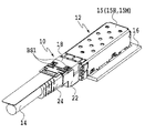
- FIG. 2 is a perspective view showing an appearance of an example of a transceiver module assembly and receptacle assembly according to the present invention, together with a printed wiring board.
- FIG. 3 is a perspective view showing an example of a transceiver module according to the present invention.
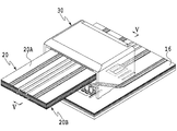
- FIG. 4 is a perspective view showing a part of a host connector and a wiring board used in an example of the receptacle assembly according to the present invention.
- FIG. 5 is a cross-sectional view taken along the line VV in FIG.
- FIG. 6 is a perspective view showing the appearance of an example of the high-speed signal connector according to the present invention.
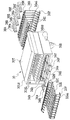
- FIG. 7 is an exploded perspective view showing the configuration of the high-speed signal connector shown in FIG.
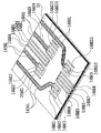
- FIG. 8 is a view showing an electrode portion and a conductor pattern of the printed wiring board shown in FIG.
- FIG. 9 is a perspective view showing a part of a host connector and a wiring board used in another example of the receptacle assembly according to the present invention.
- FIG. 10 is a diagram showing electrode portions and conductor patterns of the printed wiring board shown in FIG.
- FIG. 11A is a view showing an arrangement of contact pads on the connection end of the upper surface of the optical module substrate as a reference example.
- FIG. 11B is a diagram showing an arrangement of contact pads on the lower connection end facing the upper connection end of the optical module substrate shown in FIG. 11A.
- FIG. 12A is a perspective view including a partial cross section of the plug connector used in another example of the transceiver module according to the present invention and the configuration of the host connector to which the plug connector is connected. 12B is a cross-sectional view showing the configuration of the example shown in FIG. 12A together with the printed wiring board.
- FIG. 2 shows an example of a transceiver module assembly and receptacle assembly according to the invention together with a wiring board.
- the transceiver module assembly comprises a transceiver module (hereinafter also referred to as an optical module) 10 to which an optical connector 24 connected to one end of an optical fiber cable 14 as an optical cable is detachably connected, and an optical module
- the optical module receptacle assembly 12 to which 10 is connected is configured as a main element.
- the optical module 10 corresponds to, for example, a communication speed of 56 Gbs or more, and the optical module substrate 20 (see FIG. 4), the upper case 18 covering the upper portion of the optical module substrate 20, and the optical module substrate 20 And a lower case 22 covering the lower part of the lower case.
- the upper case 18 is formed of, for example, a metal material having excellent thermal conductivity, and has a recess (not shown) in which the upper portion of the optical module substrate 20 is accommodated. Through holes (not shown) communicating with the concave portion are formed in two places at predetermined intervals in the upper wall portion forming the concave portion. A small screw BS1 for fixing the upper case 18 to the optical module substrate 20 and the lower case 22 described later is inserted into each through hole.
- the lower case 22 is formed of, for example, a metal material having excellent thermal conductivity, and has a relatively shallow recess (not shown) in which the lower portion of the optical module substrate 20 is accommodated.
- the optical module substrate 20 supports a connector support member (not shown) that accommodates and supports a receptacle (not shown) to which the optical connector 24 is connected, supports the connector support member, and also has a light emitting / receiving element unit etc. It is comprised including the board part mounted in a mounting surface as a main element.
- the contact end of the substrate portion is a contact pad having a thickness of about 1 mm and comprising a plurality of contact pads formed in parallel to each other at a predetermined distance, as shown in an exaggerated manner in FIGS. 1A and 1B.
- the groups 20EA, 20EB are provided on the upper surface 20A and the lower surface 20B (see FIG. 5) at one end.
- Contact pad groups 20EA and 20EB are electrically connected to the conductor patterns in the substrate portion.
- the connection end portion of the substrate portion and the end portion provided with the above-described connector support member are electrically connected via a conductor formed inside.
- the contact pad group 20EA formed on the upper surface 20A at the connection end of the substrate portion is, for example, as shown in FIG. 1A, a contact pad 20A1 which is conducted to the ground line (G) sequentially from the end, Contact pads 20A2 and 20A3 conducting to the high speed signal line (S), a contact pad 20A4 conducting to the ground line (G), power contact pads 20A5 and 20A6 conducting to the power supply line, and a ground line (G) It comprises a contact pad 20A7 conducting, a contact pad 20A8 and 20A9 conducting to the high speed signal line (S) on the receiving side, a contact pad 20A10 conducting to the ground line (G), and a spare contact pad 20A11. ing. That is, the contact pad group 20EA is composed of eleven contact pads.
- the contact pad group 20EB formed on the lower surface 20B at the connection end of the substrate portion is, for example, as shown in FIG. 1B, a contact pad 20B1 which conducts sequentially to the ground line (G) from the end, Contact pads 20B2 and 20B3 conducting to the high speed signal line (S), contact pads 20B4 conducting to the ground line (G), and contact pads 20B5, 20B6 and 20B7 conducting to the low speed signal line (S), Contact pad 20B8 conducting to ground line (G), contact pad 20B9 conducting to high speed signal line (S) on the receiving side, 20B10, and contact pad 20B11 conducting to ground line (G) It is configured. That is, the contact pad group 20EB is configured of eleven contact pads. The contact pad group 20EB is biased to one side with respect to the above-mentioned contact pad group 20EA along the arrangement direction of the contact pads.
- the optical module receptacle assembly 12 is fixed on, for example, a printed wiring board 16 in a predetermined electronic device.
- the optical module receptacle assembly 12 includes a receptacle cage 15 forming an outer shell thereof, and a host connector 30 disposed in a host connector accommodating portion 15H formed in the receptacle cage 15 (see FIGS. 4 to 6). Is composed including.
- the receptacle cage 15 is formed of, for example, a metal material, and has a host connector housing portion 15H inside.
- the host connector housing portion 15H communicates with a module insertion port at one side of the receptacle cage 15.
- a space (module housing portion 15M) into which the connection end of the optical module 10 is inserted is formed between one end of the host connector 30 in the host connector housing portion 15H and one end of the plug insertion port.
- the host connector 30 corresponds to, for example, a communication speed of 56 Gbs or more, and a connector insulator having a slot 30SL into which the connection end of the optical module 10 is removably inserted, and a plurality of contact terminals 32ai, 36ai (i 1 to n and n are positive integers (see FIGS. 5 and 7).
- Each of the contact terminals 32ai and 36ai is to electrically connect the connection end of the optical module 10 to an electrode group connected to a conductor pattern of the printed wiring board 16 described later.
- the contact terminal 32ai is, as shown in FIGS. 5 and 7, a movable contact portion 32M having at one end a contact portion 32C to be in contact with the contact pads 20B1 to 20B11 at the connection end of the optical module 10; A fixed portion 32F having at one end a fixed terminal portion fixed by soldering to 16 electrode groups, and a connecting portion 32E connecting the other end of the movable contact portion 32M and the other end of the fixed portion 32F .
- the fixed terminal portion of the fixing portion 32F is directed in the insertion direction of the connection end portion of the optical module 10 along the X coordinate axis direction so as to be substantially parallel to the connecting portion 32E, as enlarged and shown in FIG. It is bent.
- the distance CH from the other end (curved portion) of the movable contact portion 32M to the mounting surface of the printed wiring board 16 is the printed wiring board 16 of the end portion 36fe of the slope portion in the fixed portion 36F of the contact terminal 36ai described later. It is set larger than the distance to the mounting surface.
- the Y coordinate axis is taken along the arrangement direction of the contact terminals 32 ai and 36 ai
- the X coordinate axis is taken along the attachment and detachment direction of the connection end of the optical module 10.
- the Z coordinate axis is orthogonal to the X coordinate axis and the Y coordinate axis.
- the contact terminal 36 ai is fixed by soldering to the electrode group of the printed wiring board 16 and the movable contact portion 36 M having at one end the contact portion 36 C to be in contact with the contact pads 20 A 1 to 20 A 11 at the connection end of the optical module 10 It comprises the fixed part 36F which has a terminal part at one end, and the connection part 36E which connects the other end of the movable contact part 36M and the other end of the fixed part 36F.
- the fixing terminal portion of the fixing portion 36F is bent in the insertion direction of the connection end portion of the optical module 10 so as to be substantially orthogonal to the connecting portion 36E, as enlarged and shown in FIG.
- the connector insulator is formed of a resin material, and has a slot 30SL through which the connection end of the optical module 10 passes when the optical module 10 is attached or detached.
- the slot 30SL has a maximum height of about 1.35 mm corresponding to the thickness of the connection end of the optical module 10.
- the periphery of the slot 30SL is formed to be surrounded by the side walls 30RS and 30LS and an upper portion 30T interconnecting the side walls 30RS and 30LS.
- the slot 30SL communicates with a connection end accommodating portion 30E into which the connection end of the optical module 10 is inserted.
- the minimum depth Dp in the connection end accommodating portion 30E is set to, for example, about 6.0 mm. As shown in FIG.
- a predetermined first chamfered portion C1 is applied to a portion forming the slot 30SL in the upper portion 30T of the connector insulator. Further, a predetermined second chamfered portion C2 is also applied to an end portion of the upper portion 30T of the connector insulator.
- the slit 30ASi is formed on the inner peripheral surface of the upper portion 30T, and the slit 30BSi is formed on the lower inner peripheral surface facing the slit 30ASi.
- the Y coordinate axis is taken along the arrangement direction of the contact terminals 32ai and 36ai
- the X coordinate axis is taken along the attachment and detachment direction of the connection end of the optical module 10.
- the Z coordinate axis is orthogonal to the X coordinate axis and the Y coordinate axis.
- the contact portion 36C of the movable contact portion 36M of the contact terminal 36ai and the contact portion 32C of the movable contact portion 32M of the contact terminal 32ai face each other. .
- the connection end of the optical module 10 is the movable contact of the contact terminal 36ai It is inserted between the contact portion 36C of the portion 36M and the contact portion 32C of the movable contact portion 32M of the contact terminal 32ai.
- the contact portion 36C of the movable contact portion 36M of each contact terminal 36ai abuts on the contact pad group 20EA, and the contact portion 32C of the movable contact portion 32M of each contact terminal 32ai abuts on the contact pad group 20EB.
- the maximum distance Lc from the open end face of the slot 30SL of the contact portion 36C of the movable contact portion 36M of each contact terminal 36ai and the contact portion 32C of the movable contact portion 32M of each contact terminal 32ai is set to about 3.0 mm at maximum. It is done.
- connection members 34A, 34B, 34E, and 34F connecting to each other are fitted in the recess 30R of the connector insulator.
- the connection members 34A, 34B, 34E, and 34F are arranged in a line along the Y coordinate axis in FIG. 5 in the recess 30R.
- the connecting members 34A, 34B, 34E, and 34F are each formed of, for example, a conductive resin, and the protrusions 34a, 34b, 34e, and 34f are in contact with the surface of the connecting portion 32E from below the connecting portion 32E. Have.
- connection members 38A, 38B which electrically connect the adjacent ground contact terminals 36ai to each other at the same potential, 38E and 38F are disposed parallel to one another along the Y coordinate axis in FIG. 5 (see FIG. 7).
- the connecting members 38A, 38B, 38E, and 38F integrally formed of conductive resin are disposed at predetermined intervals, and are protrusions that contact the surface of the movable contact portion 36M from above the movable contact portion 36M. It has sections 38a, 38b, 38e and 38f.
- a plurality of positioning pins 30D fitted to the positioning holes of the printed wiring board 16 are formed on the bottom of the connector insulator.
- the electrode group of the printed wiring board 16 to which the fixed terminal portion of the fixed portion 32F of the contact terminal 32ai and the fixed terminal portion of the fixed portion 36F of the contact terminal 36ai are fixed by soldering is partially illustrated in FIG. As shown in FIG. 1, it is formed at the end of the printed wiring board 16.
- the first electrode group consisting of the electrode parts 16BE1 to 16BE11 to which the fixed terminal part of the fixed part 32F of the contact terminal 32ai is soldered and fixed
- the fixed terminal part of the fixed part 36F of the contact terminal 36ai is soldered and fixed
- a second electrode group consisting of the electrode portions 16AE1 to 16AE11.
- the first electrode group is formed at a position close to the end of the printed wiring board 16, and the second electrode group is formed at a position farther from the end of the printed wiring board 16 than the first electrode group. It is formed.
- the electrode portions 16BE1 to 16BE11 in the first electrode group respectively include a contact pad 20B1 electrically connected to the ground line (G) formed on the lower surface 20B at the connection end of the above-mentioned substrate portion, and a high speed signal line Contact pads 20B2 and 20B3 conducting to S), contact pads 20B4 conducting to ground line (G), contact pads 20B5, 20B6 and 20B7 conducting to low speed control signal line (S), and ground line (G) And the contact pad 20B9 conductive to the high speed signal line (S) on the reception side, and 20B10, and the contact pad 20B11 conductive to the ground line (G).
- Electrodes 16BE2 and 16BE3 are each formed on the surface layer of printed wiring board 16 through conductor path 16THL passing a position separated from one end of the second electrode group, and another high-speed signal line (S) It is directly connected to the portion of the conductor pattern to be considered.
- the electrode portions 16BE9 and 16BE10 are formed on the surface layer of the printed wiring board 16 respectively, and other high-speed signal lines (via conductor paths 16RHL passing through a position separated from the other end of the second electrode group) It is directly connected to the portion of the conductor pattern to be S).
- the electrode portions 16AE1 to 16AE11 in the second electrode group respectively include a contact pad 20A1 electrically connected to the ground line (G) formed on the upper surface 20A at the connection end of the above-mentioned substrate portion, and a high speed signal line S) the contact pads 20A2 and A3 conducting to the ground line, the contact pad 20A4 conducting to the ground line (G), the power source contact pads 20A5 and 20A6 conducting to the power supply line, and the contact pad 20A7 conducting to the ground line (G)
- the contact pads 20A8 and 20A9 electrically connected to the high speed signal line (S) on the receiving side, the contact pads 20A10 electrically connected to the ground line (G), and the spare contact pad 20A11 are formed.
- the electrode portions 16AE2 and 16AE3 are directly connected to the portions of the conductor pattern to be another high-speed signal line (S) through the conductor path 16THL formed on the surface layer of the printed wiring board 16, respectively. Further, the electrode portions 16AE8 and 16AE9 are each directly formed on the surface layer of the printed wiring board 16 and directly connected to the portion of the conductor pattern to be another high-speed signal line (S) through the conductor path 16RHL. .
- FIG. 9 shows a part of a host connector and a wiring substrate used in another example of the receptacle assembly according to the present invention, together with the optical module substrate.
- the optical module receptacle assembly is fixed on, for example, a printed wiring board 56 in a predetermined electronic device.
- the optical module receptacle assembly includes a receptacle cage (not shown) forming an outer shell thereof and a host connector 30 'disposed in a host connector receptacle formed in the receptacle cage. .
- the host connector 30 ′ abuts on the connector insulator having a slot through which the connection end of the optical module substrate 20 passes and the lower surface 20B of the connection end A plurality of first contact terminals (not shown) and a second contact terminal (not shown) to be abutted to the upper surface 20A at the connection end.
- the configurations of the connector insulator and the second contact terminal are the same as the configurations of the insulator and the contact terminal 36ai shown in FIG.
- the first contact terminal is fixed by soldering to a movable contact portion having at one end a contact portion 32C to be in contact with the contact pads 20B1 to 20B11 at the connection end of the optical module 10, and an electrode group of the printed wiring board 56 It comprises: the fixed part which has a fixed terminal part in one end, and the connection part which connects the other end of a movable contact part, and the other end of fixed part.
- the fixed terminal portion in the fixed portion is bent in the direction in which the connection end of the optical module 10 is pulled out so as to be substantially parallel to the connection portion.
- the plurality of first contact terminals and the second contact terminals respectively electrically connect the connection end of the optical module substrate 20 to an electrode group connected to a conductor pattern of the printed wiring board 56 described later. Be done.
- the first electrode group including the electrode portions 56BE1 to 56BE11 to which the fixed terminal portion in the fixed portion of the first contact terminal is soldered and fixed, and the fixed terminal portion in the fixed portion of the second contact terminal are soldered
- a second electrode group consisting of the electrode parts 56AE1 to 56AE11 to be attached and fixed.
- a ground conductor 56G is formed between the first electrode group and the second electrode group on the mounting surface of the printed wiring board 56 so as to separate the first electrode group and the second electrode group. It is done. The formation of the ground conductor 56G connected to the ground line via the via in this manner further improves the crosstalk characteristic of the host connector 30 '.
- the first electrode group described above is formed at a position close to the end of the printed wiring board 56, and the second electrode group described above is from the end of the printed wiring board 56 more than the first electrode group. It is formed at a distant position.
- the electrode portions 56BE1 to 56BE11 in the first electrode group respectively transmit the contact pads 20B1 electrically connected to the ground line (G) formed on the lower surface 20B at the connection end of the substrate portion of the optical module substrate 20 described above, and Contact pads 20B2 and 20B3 conducting to the high speed signal line (S) on the side, a contact pad 20B4 conducting to the ground line (G), and contact pads 20B5, 20B6 and 20B7 conducting to the low speed control signal line (S) , Contact pad 20B8 conducting to the ground line (G), contact pad 20B9 conducting to the high speed signal line (S) on the receiving side, and 20B10, and contact pad 20B11 conducting to the ground line (G) It is formed.
- the electrode portions 56BE2 and 56BE3 are connected to portions of the conductor patterns 56THL2 to be high-speed signal lines (S) through the conductor paths 56THL1 and the vias 56VIA, respectively.
- One end of each conductor path 56THL1 is connected to the electrode portions 56BE2 and 56BE3 through the via 56VIA located adjacent to the electrode portions 56BE2 and 56BE3, and the other end of each conductor path 56THL1 is a position adjacent to each conductor pattern 56THL2 Are connected to the conductor patterns 56THL2 through the vias 56VIA.
- Each conductor path 56THL1 is formed in the lower layer below the ground conductor 56G formed on the surface layer of the printed wiring board 56, as shown by a broken line in FIG.
- the electrode portions 56BE9 and 56BE10 are connected to portions of a conductor pattern 56RHL2 which is a high-speed signal line (S) through the conductor paths 56RHL1 and vias 56VIA, respectively.
- One end of conductor path 56RHL1 is connected to electrode portions 56BE9 and 56BE10 through via 56VIA located adjacent to electrode portions 56BE9 and 56BE10, and the other end of conductor path 56RHL1 is located adjacent to conductor pattern 56RHL2
- Each conductor pattern 56THL2 is connected through 56VIA.
- Each conductor path 56RHL1 is formed in a lower layer below the ground conductor 56G formed on the surface layer of the printed wiring board 56, as shown by a broken line in FIG.
- the electrode parts 56AE1 to 56AE11 in the second electrode group respectively include a contact pad 20A1 electrically connected to the ground line (G) formed on the upper surface 20A at the connection end of the above-mentioned substrate part, and a high speed signal line S) the contact pads 20A2 and A3 conducting to the ground line, the contact pad 20A4 conducting to the ground line (G), the power source contact pads 20A5 and 20A6 conducting to the power supply line, and the contact pad 20A7 conducting to the ground line (G)
- the contact pads 20A8 and 20A9 electrically connected to the high speed signal line (S) on the receiving side, the contact pads 20A10 electrically connected to the ground line (G), and the spare contact pad 20A11 are formed.
- the electrode portions 56AE2 and 56AE3 are directly connected to the portions of the conductor pattern to be another high-speed signal line (S) through the conductor paths 56THL formed on the surface layer of the printed wiring board 56, respectively. Also, the electrode portions 56AE8 and 56AE9 are respectively formed directly on the surface layer of the printed wiring board 56 and directly connected to the portions of the conductor pattern to be another high-speed signal line (S) through the conductor paths 56RHL. .
- the optical module substrate 20 used in one example of the transceiver module according to the present invention can increase the number of channels as compared with the optical module substrate 40 as a reference example shown in FIGS. 11A and 11B described later.
- the structure and conductor pattern of the printed wiring board 16 used in an example of the receptacle assembly according to the present invention shown in FIG. 8 correspond to the arrangement of the contact pads of the optical module substrate 20 while maintaining the vias and the like. Since it is manufactured without using it, it is simplified as compared with the conductor pattern of the printed wiring board 56 shown in FIG.
- FIGS. 11A and 11B schematically show a reference example of the optical module substrate 40 in the optical module which is attachable to and detachable from the above-mentioned host connectors 30 and 30 ′.
- An optical module substrate 40 in the optical module supports a connector support member (not shown) that accommodates and supports a receptacle (not shown) to which the optical connector is connected, and supports the connector support member and also emits light / light receiving element
- a unit etc. is comprised including the board
- connection end portion of the substrate portion is, as shown in an exaggerated manner in FIGS. 11A and 11B, a contact pad group 40EA, 40EB consisting of a plurality of contact pads formed in parallel with each other at a predetermined interval, 40A and the lower surface 40B.
- the contact pad groups 40EA and 40EB are each electrically connected to the conductor pattern in the substrate portion.
- the connection end portion of the substrate portion and the end portion provided with the above-described connector support member are electrically connected via a conductor formed inside.
- the contact pad group 40EA formed on the upper surface 40A at the connection end of the substrate portion is, for example, as shown in FIG. 11A, a contact pad 40A1 conducted to the ground line (G) sequentially from the end, Contact pads 40A2 and 40A3 conducting to the high-speed signal line (S), contact pads 40A4 conducting to the ground line (G), power contact pads 40A5 and 40A6 conducting to the power supply line, and the ground line (G)
- the contact pad 40A7 is conductive, the contact pads 40A8 and 40A9 conductive to the high speed signal line (S) on the reception side, and the contact pad 40A10 conductive to the ground line (G). That is, the contact pad group 40EA is composed of ten contact pads.
- the contact pad group 40EB formed on the lower surface 40B at the connection end of the substrate portion is, for example, as shown in FIG. 11B, the contact pad 40B1 which conducts sequentially to the ground line (G) from the end, and low speed control Contact pads 40B2 and 40B3 conducting to the signal line (S), contact pads 40B4, 40B5 and 40B6 conducting to the slow control signal line (S), and a contact pad 40B7 conducting to the slow control signal line (S) 40B8 and contact pads 40B9 and 40B10 electrically connected to the ground line (G). That is, the contact pad group 40EB is configured of ten contact pads.
- 20B6, and 20B7, and the contact pads 40B4, 40B5, and 40B6 can be electrically connected to the electrode portions 16BE5, 16BE6, and 16BE7 through the contact terminals 32ai, respectively.
- the optical module substrate 40 having a smaller number of channels than the module substrate 20 can be connected to the above-described host connectors 30 and 30 '.
- connection ends of the substrate portion of the optical module substrate 20 used in one example of the above-described transceiver module assembly according to the present invention are a plurality of contact pads formed parallel to each other at a predetermined distance.
- the contact pads 20EA and 20EB at one end on the upper surface 20A and the lower surface 20B are not limited to such an example.
- the connection end of the substrate portion 60 may be connected to the plug connector 62.
- the contact pads 60Ei are arranged at predetermined intervals in a row in a direction substantially orthogonal to the insertion direction of the module substrate 60 with respect to the plug connector 62.
- the arrangement of contact pads 60Ei on the front and back sides may be identical to the arrangement of contact pads 20EA and contact pads 20EB as shown in, for example, FIGS.
- the arrangement of the contact pads 60Ei on the back surface includes a pair of contact pads conductive to at least the high speed signal line (S) on the transmission side and a pair of contact pads conductive to the high speed signal line (S) on the reception side. It may be configured as follows.
- connection end 62PE is inserted into a slot of a host connector 70 described later.
- the connection end 62PE has a recess 62R in which the end of the module substrate 60 is inserted.
- the recess 62R is in communication with the open end of the substrate support.
- the both sides in the recessed part 62R are formed of the side wall part.
- grooves 62Rg for guiding the side portion of the module substrate 60 are formed on both side walls forming the recess 62R so as to keep the posture of the module substrate 60 parallel to the upper surface of the connection end 62PE.
- the substrate support of the plug connector 62 has an open end through which the end of the inserted module substrate 60 passes.
- a pair of positioning portions 16A that are in contact with the substrate support wall (not shown) in the upper case and the lower case of the optical module are formed separately from each other.
- an elongated spring portion 62B is formed to be in contact with a substrate support wall (not shown) in the upper case and the lower case.
- the contact terminals 62EAi are arranged on the top surface of the connection end 62PE facing the pair of positioning portions 62A of the substrate support portion with a predetermined interval corresponding to the above-mentioned contact pad 60Ei.
- the contact terminal 62EAi includes, for example, a power supply terminal, a signal contact terminal, and a grounding contact terminal. For example, a pair of adjacent signal contact terminals is disposed between the ground contact terminals.
- the contact terminal 62EAi has a fixed terminal portion soldered and fixed to the contact pad 60Ei, and a contact portion to be in contact with the contact portion of the contact terminal 74ai of the host connector 70.
- the contact terminals 62EBi are arranged on the lower surface of the connection end 62PE facing the spring portion 62B of the substrate support portion at a predetermined interval corresponding to the above-mentioned contact pad 60Ei.
- the contact terminal 62EBi includes, for example, a power supply terminal, a signal contact terminal, and a grounding contact terminal. For example, a pair of adjacent signal contact terminals is disposed between the ground contact terminals.
- the contact terminal 62EBi has a fixed terminal portion soldered and fixed to the contact pad 60Ei, and a contact portion abutted against the contact portion of the contact terminal 72ai of the host connector 70.
- Each of the contact terminals 72ai and 74ai electrically connects the connection end 62PE of the plug connector 62 to an electrode group connected to a conductor pattern of the printed wiring board 76 described later.
- the contact terminal 72ai is, as shown in FIG. 12B, a movable contact portion 72M having at one end a contact portion 72C to be in contact with the contact terminal 62EBi at the connection end 62PE of the plug connector 62, and an electrode group of the printed wiring board 76 And a connecting portion 72E for connecting the other end of the movable contact portion 72M and the other end of the fixed portion 72F.
- the fixed terminal portion of the fixing portion 72F is bent in the insertion direction of the connection end 62PE of the plug connector 62 along the X coordinate axis direction so as to be substantially parallel to the connecting portion 72E.
- the Y coordinate axis is taken along the arrangement direction of the contact terminals 72ai and 74ai, and the X coordinate axis is taken along the attachment and detachment direction of the connection end 62PE of the plug connector 62.
- the Z coordinate axis is orthogonal to the X coordinate axis and the Y coordinate axis.
- the contact terminal 74 ai is a movable contact 74 M having at one end a contact portion 74 C that contacts the contact terminal 62 EAi at the connection end 62 PE of the plug connector 62, and a fixed terminal soldered to the electrode group of the printed wiring board 76. It comprises the fixed part 74F which has a part at one end, and the connection part 74E which connects the other end of the movable contact part 74M and the other end of the fixed part 74F.
- the fixed terminal portion of the fixing portion 74F is bent in the insertion direction of the connection end 62PE of the plug connector 62 so as to be substantially orthogonal to the connecting portion 74E.
- the movable contact portion 74M extends substantially parallel to the mounting surface of the printed wiring board 76, and the connecting portion 74E is bent from the end of the movable contact portion 74M so as to be substantially perpendicular to the mounting surface of the printed wiring board 76 It is done.
- the connector insulator is formed of a resin material and has a slot through which the connection end 62 PE of the plug connector 62 passes when the optical module is attached or detached.
- the slot has a maximum height corresponding to the thickness of the connection end 62 PE of the plug connector 62.
- the periphery of the slot is formed to be surrounded by the side wall portion and the upper portion interconnecting the both side wall portions.
- the slot communicates with a connection end accommodating portion 70E in which the connection end 62PE of the plug connector 62 is inserted.
- a plurality of slits 70ASi and 70BSi (i 1 to n, n is a positive integer) formed at predetermined intervals along the Y coordinate axis shown in FIG. 12B.
- the slit 70ASi is formed on the upper inner circumferential surface
- the slit 70BSi is formed on the lower inner circumferential surface facing the slit 70ASi.
- the contact portion 72C of the movable contact portion 72M of the contact terminal 72ai and the contact portion 74C of the movable contact portion 74M of the contact terminal 74ai are disposed to face each other.
- the connection end 62PE of the plug connector 62 is inserted into the connection end accommodating portion 70E via the slot as shown in FIG. 12B, the connection end 62PE of the plug connector 62 is a movable contact of the contact terminal 72ai. It is inserted between the contact portion 72C of the portion 72M and the contact portion 74C of the movable contact portion 74M of the contact terminal 74ai.
- the heat sink is provided on the receptacle cage 15 so as to dissipate the heat generated from the optical module 10 through the heat sink (not shown).
Landscapes
- Physics & Mathematics (AREA)
- Engineering & Computer Science (AREA)
- Microelectronics & Electronic Packaging (AREA)
- Electromagnetism (AREA)
- General Physics & Mathematics (AREA)
- Optics & Photonics (AREA)
- Coupling Device And Connection With Printed Circuit (AREA)
- Optical Couplings Of Light Guides (AREA)
- Details Of Connecting Devices For Male And Female Coupling (AREA)
- Connector Housings Or Holding Contact Members (AREA)
Abstract
Dans la présente invention, un groupe de plages de contact (20EB), qui est formé sur la surface inférieure (20B) d'une section d'extrémité de connexion dans la partie de base d'une carte de module optique (20), est constitué, séquentiellement en partant du bord supérieur, d'une plage de contact (20B1) qui établit une connexion conductrice avec une ligne de masse (G), des plages de contact (20B2) et (20B3) qui établissent une connexion conductrice avec une ligne de signaux haute-vitesse (S) côté émission, une plage de contact (20B4) qui établit une connexion conductrice avec la ligne de masse (G), des plages de contact (20B5, 20B6 et 20B7) qui établissent des connexions conductrices avec une ligne de signaux basse vitesse (S), une plage de contact (20B8) qui établit une connexion conductrice avec la ligne de masse (G), des plages de contact (20B9 et 20B10) qui établissent une connexion conductrice avec une ligne de signaux haute-vitesse (S) côté réception, et une plage de contact (20B11) qui établit une connexion conductrice avec la ligne de masse (G). Dans un connecteur hôte (30), des parties de bornes fixes d'une pluralité de bornes de contact (32ai) à connecter aux plages de contact (20B2 et 20B3), qui établissent une connexion conductrice à la ligne de signaux haute vitesse (S) côté émission et aux plages de contact (20B9 et 20B10) qui établissent une connexion conductrice à la ligne de signaux haute-vitesse (S) côté réception, sont connectées électriquement, au moyen d'une partie d'électrode (16BE2), d'une partie d'électrode (16BE3), d'une partie d'électrode (16BE9) et d'une partie d'électrode (16BE10) dans une carte de circuit imprimé (16), à des chemins conducteurs (16THL, 16RHL) qui se prolongent dans une ligne de signaux haute vitesse formée sur un plan qui est commun à la partie d'électrode (16BE2), à la partie d'électrode (16BE3), à la partie d'électrode (16BE9) et à la partie d'électrode (16BE10).
Priority Applications (4)
| Application Number | Priority Date | Filing Date | Title |
|---|---|---|---|
| CN201780094765.8A CN111095682B (zh) | 2017-12-14 | 2017-12-14 | 高速信号用连接器及具备其的插座组件、收发器模块组件 |
| JP2019559507A JP7161113B2 (ja) | 2017-12-14 | 2017-12-14 | 高速信号用コネクタ、および、それを備えるリセプタクルアセンブリ、トランシーバモジュールアセンブリ |
| PCT/JP2017/044956 WO2019116516A1 (fr) | 2017-12-14 | 2017-12-14 | Ensemble réceptacle et connecteur à signal haute-vitesse et ensemble module émetteur-récepteur équipé de celui-ci |
| US16/772,126 US11600950B2 (en) | 2017-12-14 | 2017-12-14 | High-speed signal connector and receptacle assembly equipped therewith and transceiver module assembly equipped therewith |
Applications Claiming Priority (1)
| Application Number | Priority Date | Filing Date | Title |
|---|---|---|---|
| PCT/JP2017/044956 WO2019116516A1 (fr) | 2017-12-14 | 2017-12-14 | Ensemble réceptacle et connecteur à signal haute-vitesse et ensemble module émetteur-récepteur équipé de celui-ci |
Publications (1)
| Publication Number | Publication Date |
|---|---|
| WO2019116516A1 true WO2019116516A1 (fr) | 2019-06-20 |
Family
ID=66819134
Family Applications (1)
| Application Number | Title | Priority Date | Filing Date |
|---|---|---|---|
| PCT/JP2017/044956 Ceased WO2019116516A1 (fr) | 2017-12-14 | 2017-12-14 | Ensemble réceptacle et connecteur à signal haute-vitesse et ensemble module émetteur-récepteur équipé de celui-ci |
Country Status (4)
| Country | Link |
|---|---|
| US (1) | US11600950B2 (fr) |
| JP (1) | JP7161113B2 (fr) |
| CN (1) | CN111095682B (fr) |
| WO (1) | WO2019116516A1 (fr) |
Families Citing this family (14)
| Publication number | Priority date | Publication date | Assignee | Title |
|---|---|---|---|---|
| CN104704682B (zh) | 2012-08-22 | 2017-03-22 | 安费诺有限公司 | 高频电连接器 |
| CN110247219B (zh) | 2014-01-22 | 2021-06-15 | 安费诺有限公司 | 电连接器 |
| WO2018039164A1 (fr) | 2016-08-23 | 2018-03-01 | Amphenol Corporation | Connecteur configurable pour hautes performances |
| TWI889666B (zh) | 2019-02-19 | 2025-07-11 | 美商安芬諾股份有限公司 | 電連接器及用於製造電連接器之方法 |
| US11316304B2 (en) | 2019-09-07 | 2022-04-26 | Dongguan Luxshare Technologies Co., Ltd | Electrical connector with improved electrical performance |
| WO2021154702A1 (fr) | 2020-01-27 | 2021-08-05 | Fci Usa Llc | Connecteur à vitesse élevée |
| CN114077020A (zh) * | 2020-08-18 | 2022-02-22 | 华为技术有限公司 | 复合模块及其制造方法 |
| CN215816516U (zh) | 2020-09-22 | 2022-02-11 | 安费诺商用电子产品(成都)有限公司 | 电连接器 |
| CN213636403U (zh) * | 2020-09-25 | 2021-07-06 | 安费诺商用电子产品(成都)有限公司 | 电连接器 |
| CN214957657U (zh) * | 2021-04-23 | 2021-11-30 | 东莞富强电子有限公司 | 高速连接器 |
| EP4125310A1 (fr) | 2021-07-29 | 2023-02-01 | Aptiv Technologies Limited | Système de connexion de carte de circuit imprimé, appareil et procédé |
| CN115706104A (zh) * | 2021-08-13 | 2023-02-17 | 华为技术有限公司 | 一种在板光互连装置及通信设备 |
| CN216850408U (zh) * | 2022-01-05 | 2022-06-28 | 东莞立讯技术有限公司 | 电连接器 |
| CN116073195A (zh) * | 2023-02-27 | 2023-05-05 | 苏州浪潮智能科技有限公司 | Ocp网卡线缆的ncsi信号优化装置及其制备方法 |
Citations (6)
| Publication number | Priority date | Publication date | Assignee | Title |
|---|---|---|---|---|
| JP2002334755A (ja) * | 2001-04-27 | 2002-11-22 | Molex Inc | 基板用コネクタ |
| JP2007141587A (ja) * | 2005-11-16 | 2007-06-07 | Japan Aviation Electronics Industry Ltd | コネクタ及びコネクタ組立体 |
| JP2013004518A (ja) * | 2011-06-10 | 2013-01-07 | Tyco Electronics Singapore Pte Ltd | 電気コネクタ |
| JP2015115148A (ja) * | 2013-12-10 | 2015-06-22 | 日立金属株式会社 | 基板ユニット |
| JP2015179569A (ja) * | 2014-03-18 | 2015-10-08 | 日立金属株式会社 | 通信モジュール及び通信モジュール用コネクタ |
| JP2016225242A (ja) * | 2015-06-03 | 2016-12-28 | パナソニックIpマネジメント株式会社 | 光電気変換装置及び接続装置 |
Family Cites Families (29)
| Publication number | Priority date | Publication date | Assignee | Title |
|---|---|---|---|---|
| US5162002A (en) * | 1990-03-30 | 1992-11-10 | Molex Incorporated | Card edge connector assembly |
| EP0529345B1 (fr) | 1991-08-05 | 1996-12-11 | Molex Incorporated | Assemblage de connecteur de bordure de carte |
| US6135781A (en) * | 1996-07-17 | 2000-10-24 | Minnesota Mining And Manufacturing Company | Electrical interconnection system and device |
| US7446261B2 (en) * | 2001-09-06 | 2008-11-04 | Finisar Corporation | Flexible circuit boards with tooling cutouts for optoelectronic modules |
| US7204648B2 (en) * | 2002-03-19 | 2007-04-17 | Finisar Corporation | Apparatus for enhancing impedance-matching in a high-speed data communications system |
| US7044752B2 (en) * | 2002-05-24 | 2006-05-16 | Fci Americas Technology, Inc. | Receptacle |
| US6644995B1 (en) * | 2002-08-05 | 2003-11-11 | Hon Hai Precision Ind. Co., Ltd. | Low insertion force electrical connector |
| WO2006010099A1 (fr) * | 2004-07-07 | 2006-01-26 | Molex Incorporated | Ensemble de connecteur de bord de carte muni de bornes haut debit |
| US7798820B2 (en) | 2006-04-04 | 2010-09-21 | Finisar Corporation | Communications module edge connector having multiple communication interface pads |
| JP4776483B2 (ja) | 2006-09-20 | 2011-09-21 | 富士通株式会社 | コネクタ実装構造 |
| JP2010108800A (ja) * | 2008-10-31 | 2010-05-13 | Japan Aviation Electronics Industry Ltd | コネクタ |
| US8545240B2 (en) * | 2008-11-14 | 2013-10-01 | Molex Incorporated | Connector with terminals forming differential pairs |
| US7833068B2 (en) * | 2009-01-14 | 2010-11-16 | Tyco Electronics Corporation | Receptacle connector for a transceiver assembly |
| US8932081B2 (en) * | 2009-07-01 | 2015-01-13 | Molex Incorporated | Connector with terminal retention |
| CN102714363B (zh) * | 2009-11-13 | 2015-11-25 | 安费诺有限公司 | 高性能小形状因数的连接器 |
| JP5019187B2 (ja) | 2010-01-29 | 2012-09-05 | 山一電機株式会社 | コネクタ |
| US8267718B2 (en) * | 2010-04-07 | 2012-09-18 | Panduit Corp. | High data rate electrical connector and cable assembly |
| US8328565B2 (en) * | 2010-07-23 | 2012-12-11 | Tyco Electronics Corporation | Transceiver assembly having an improved receptacle connector |
| US8721193B2 (en) * | 2010-08-13 | 2014-05-13 | Finisar Corporation | Electronic module having multiple flex circuit connectors |
| CN102593661B (zh) * | 2011-01-14 | 2014-07-02 | 富士康(昆山)电脑接插件有限公司 | 电连接器 |
| US8727793B2 (en) * | 2011-03-11 | 2014-05-20 | Cisco Technology, Inc. | Optical module design in an SFP form factor to support increased rates of data transmission |
| CN102832480B (zh) * | 2011-06-16 | 2016-02-03 | 富士康(昆山)电脑接插件有限公司 | 电连接器 |
| US8371861B1 (en) * | 2011-08-03 | 2013-02-12 | Tyco Electronics Corporation | Straddle mount connector for a pluggable transceiver module |
| JP5298227B1 (ja) | 2012-07-19 | 2013-09-25 | イリソ電子工業株式会社 | コネクタ |
| CN104183986B (zh) * | 2013-05-24 | 2017-06-20 | 富士康(昆山)电脑接插件有限公司 | 插头连接器 |
| US9692183B2 (en) * | 2015-01-20 | 2017-06-27 | Te Connectivity Corporation | Receptacle connector with ground bus |
| CN104852204B (zh) * | 2015-05-05 | 2024-03-29 | 连展科技(深圳)有限公司 | 插座电连接器 |
| WO2017106876A1 (fr) | 2015-12-17 | 2017-06-22 | Finisar Corporation | Connecteur de données à haut débit |
| JP6982962B2 (ja) * | 2017-02-16 | 2021-12-17 | 日本ルメンタム株式会社 | 光モジュール |
-
2017
- 2017-12-14 WO PCT/JP2017/044956 patent/WO2019116516A1/fr not_active Ceased
- 2017-12-14 US US16/772,126 patent/US11600950B2/en active Active
- 2017-12-14 CN CN201780094765.8A patent/CN111095682B/zh active Active
- 2017-12-14 JP JP2019559507A patent/JP7161113B2/ja active Active
Patent Citations (6)
| Publication number | Priority date | Publication date | Assignee | Title |
|---|---|---|---|---|
| JP2002334755A (ja) * | 2001-04-27 | 2002-11-22 | Molex Inc | 基板用コネクタ |
| JP2007141587A (ja) * | 2005-11-16 | 2007-06-07 | Japan Aviation Electronics Industry Ltd | コネクタ及びコネクタ組立体 |
| JP2013004518A (ja) * | 2011-06-10 | 2013-01-07 | Tyco Electronics Singapore Pte Ltd | 電気コネクタ |
| JP2015115148A (ja) * | 2013-12-10 | 2015-06-22 | 日立金属株式会社 | 基板ユニット |
| JP2015179569A (ja) * | 2014-03-18 | 2015-10-08 | 日立金属株式会社 | 通信モジュール及び通信モジュール用コネクタ |
| JP2016225242A (ja) * | 2015-06-03 | 2016-12-28 | パナソニックIpマネジメント株式会社 | 光電気変換装置及び接続装置 |
Also Published As
| Publication number | Publication date |
|---|---|
| US20210075163A1 (en) | 2021-03-11 |
| CN111095682B (zh) | 2022-03-04 |
| CN111095682A (zh) | 2020-05-01 |
| JPWO2019116516A1 (ja) | 2020-10-22 |
| JP7161113B2 (ja) | 2022-10-26 |
| US11600950B2 (en) | 2023-03-07 |
Similar Documents
| Publication | Publication Date | Title |
|---|---|---|
| JP7161113B2 (ja) | 高速信号用コネクタ、および、それを備えるリセプタクルアセンブリ、トランシーバモジュールアセンブリ | |
| TWI755293B (zh) | 插座組件 | |
| CN102570099B (zh) | 插座连接器 | |
| US8353707B2 (en) | Electrical connector assembly having a receptacle with three rows of contacts and a printed circuit board with three rows of pads | |
| CN106450945B (zh) | 用于电连接器系统的馈通式适配器组件 | |
| TWI424630B (zh) | 具有放大的插座介面之模組電氣連接器 | |
| US8475210B2 (en) | Electrical connector assembly with high signal density | |
| JP6053378B2 (ja) | ストラドルマウントコネクタ | |
| EP2281345B1 (fr) | Module d'émetteur-récepteur avec cartes de circuits imprimés doubles | |
| CN107039855B (zh) | 具有指示灯的笼式电连接器组件 | |
| CN103703396B (zh) | 多通道rf馈入装置 | |
| WO2017195714A1 (fr) | Module émetteur-récepteur, ensemble prise pour module émetteur-récepteur, et ensemble module émetteur-récepteur | |
| US20130034977A1 (en) | Receptacle connector for a pluggable transceiver module | |
| JPH10270133A (ja) | 一体化されたpcbアセンブリを有するコネクタ | |
| US8371882B1 (en) | Straddle mount connector for a pluggable transceiver module | |
| US9739967B2 (en) | Wiring member | |
| TW202017265A (zh) | 用於高頻信號之混合式電連接器 | |
| KR20110118678A (ko) | 연결 관리 시스템에 사용되는 카세트 | |
| JP6914034B2 (ja) | 光モジュール及び伝送装置 | |
| US20150255935A1 (en) | Communication Module and Communication Module Connector | |
| JP7014367B2 (ja) | 光モジュール | |
| US9373906B2 (en) | Communication module and communication module connector | |
| JP2007264438A (ja) | 光トランシーバ | |
| JP2015176827A (ja) | 通信モジュール及び通信モジュール用コネクタ |
Legal Events
| Date | Code | Title | Description |
|---|---|---|---|
| 121 | Ep: the epo has been informed by wipo that ep was designated in this application |
Ref document number: 17934750 Country of ref document: EP Kind code of ref document: A1 |
|
| ENP | Entry into the national phase |
Ref document number: 2019559507 Country of ref document: JP Kind code of ref document: A |
|
| NENP | Non-entry into the national phase |
Ref country code: DE |
|
| 122 | Ep: pct application non-entry in european phase |
Ref document number: 17934750 Country of ref document: EP Kind code of ref document: A1 |