WO2019128306A1 - 图像数据读取方法、装置、电子设备及可读存储介质 - Google Patents
图像数据读取方法、装置、电子设备及可读存储介质 Download PDFInfo
- Publication number
- WO2019128306A1 WO2019128306A1 PCT/CN2018/104861 CN2018104861W WO2019128306A1 WO 2019128306 A1 WO2019128306 A1 WO 2019128306A1 CN 2018104861 W CN2018104861 W CN 2018104861W WO 2019128306 A1 WO2019128306 A1 WO 2019128306A1
- Authority
- WO
- WIPO (PCT)
- Prior art keywords
- image
- image data
- data
- row
- block
- Prior art date
- Legal status (The legal status is an assumption and is not a legal conclusion. Google has not performed a legal analysis and makes no representation as to the accuracy of the status listed.)
- Ceased
Links
Images


Classifications
-
- G—PHYSICS
- G09—EDUCATION; CRYPTOGRAPHY; DISPLAY; ADVERTISING; SEALS
- G09G—ARRANGEMENTS OR CIRCUITS FOR CONTROL OF INDICATING DEVICES USING STATIC MEANS TO PRESENT VARIABLE INFORMATION
- G09G5/00—Control arrangements or circuits for visual indicators common to cathode-ray tube indicators and other visual indicators
- G09G5/36—Control arrangements or circuits for visual indicators common to cathode-ray tube indicators and other visual indicators characterised by the display of a graphic pattern, e.g. using an all-points-addressable [APA] memory
- G09G5/39—Control of the bit-mapped memory
- G09G5/395—Arrangements specially adapted for transferring the contents of the bit-mapped memory to the screen
- G09G5/397—Arrangements specially adapted for transferring the contents of two or more bit-mapped memories to the screen simultaneously, e.g. for mixing or overlay
-
- G—PHYSICS
- G06—COMPUTING OR CALCULATING; COUNTING
- G06F—ELECTRIC DIGITAL DATA PROCESSING
- G06F3/00—Input arrangements for transferring data to be processed into a form capable of being handled by the computer; Output arrangements for transferring data from processing unit to output unit, e.g. interface arrangements
- G06F3/14—Digital output to display device ; Cooperation and interconnection of the display device with other functional units
- G06F3/147—Digital output to display device ; Cooperation and interconnection of the display device with other functional units using display panels
-
- G—PHYSICS
- G06—COMPUTING OR CALCULATING; COUNTING
- G06F—ELECTRIC DIGITAL DATA PROCESSING
- G06F1/00—Details not covered by groups G06F3/00 - G06F13/00 and G06F21/00
- G06F1/04—Generating or distributing clock signals or signals derived directly therefrom
- G06F1/08—Clock generators with changeable or programmable clock frequency
-
- G—PHYSICS
- G06—COMPUTING OR CALCULATING; COUNTING
- G06F—ELECTRIC DIGITAL DATA PROCESSING
- G06F13/00—Interconnection of, or transfer of information or other signals between, memories, input/output devices or central processing units
- G06F13/14—Handling requests for interconnection or transfer
- G06F13/16—Handling requests for interconnection or transfer for access to memory bus
-
- G—PHYSICS
- G06—COMPUTING OR CALCULATING; COUNTING
- G06T—IMAGE DATA PROCESSING OR GENERATION, IN GENERAL
- G06T1/00—General purpose image data processing
- G06T1/60—Memory management
-
- G—PHYSICS
- G09—EDUCATION; CRYPTOGRAPHY; DISPLAY; ADVERTISING; SEALS
- G09G—ARRANGEMENTS OR CIRCUITS FOR CONTROL OF INDICATING DEVICES USING STATIC MEANS TO PRESENT VARIABLE INFORMATION
- G09G5/00—Control arrangements or circuits for visual indicators common to cathode-ray tube indicators and other visual indicators
- G09G5/36—Control arrangements or circuits for visual indicators common to cathode-ray tube indicators and other visual indicators characterised by the display of a graphic pattern, e.g. using an all-points-addressable [APA] memory
- G09G5/39—Control of the bit-mapped memory
- G09G5/395—Arrangements specially adapted for transferring the contents of the bit-mapped memory to the screen
-
- G—PHYSICS
- G09—EDUCATION; CRYPTOGRAPHY; DISPLAY; ADVERTISING; SEALS
- G09G—ARRANGEMENTS OR CIRCUITS FOR CONTROL OF INDICATING DEVICES USING STATIC MEANS TO PRESENT VARIABLE INFORMATION
- G09G5/00—Control arrangements or circuits for visual indicators common to cathode-ray tube indicators and other visual indicators
- G09G5/36—Control arrangements or circuits for visual indicators common to cathode-ray tube indicators and other visual indicators characterised by the display of a graphic pattern, e.g. using an all-points-addressable [APA] memory
- G09G5/39—Control of the bit-mapped memory
- G09G5/399—Control of the bit-mapped memory using two or more bit-mapped memories, the operations of which are switched in time, e.g. ping-pong buffers
-
- G—PHYSICS
- G09—EDUCATION; CRYPTOGRAPHY; DISPLAY; ADVERTISING; SEALS
- G09G—ARRANGEMENTS OR CIRCUITS FOR CONTROL OF INDICATING DEVICES USING STATIC MEANS TO PRESENT VARIABLE INFORMATION
- G09G2300/00—Aspects of the constitution of display devices
- G09G2300/02—Composition of display devices
- G09G2300/026—Video wall, i.e. juxtaposition of a plurality of screens to create a display screen of bigger dimensions
-
- G—PHYSICS
- G09—EDUCATION; CRYPTOGRAPHY; DISPLAY; ADVERTISING; SEALS
- G09G—ARRANGEMENTS OR CIRCUITS FOR CONTROL OF INDICATING DEVICES USING STATIC MEANS TO PRESENT VARIABLE INFORMATION
- G09G2310/00—Command of the display device
- G09G2310/08—Details of timing specific for flat panels, other than clock recovery
-
- G—PHYSICS
- G09—EDUCATION; CRYPTOGRAPHY; DISPLAY; ADVERTISING; SEALS
- G09G—ARRANGEMENTS OR CIRCUITS FOR CONTROL OF INDICATING DEVICES USING STATIC MEANS TO PRESENT VARIABLE INFORMATION
- G09G2360/00—Aspects of the architecture of display systems
- G09G2360/12—Frame memory handling
- G09G2360/122—Tiling
-
- G—PHYSICS
- G09—EDUCATION; CRYPTOGRAPHY; DISPLAY; ADVERTISING; SEALS
- G09G—ARRANGEMENTS OR CIRCUITS FOR CONTROL OF INDICATING DEVICES USING STATIC MEANS TO PRESENT VARIABLE INFORMATION
- G09G2360/00—Aspects of the architecture of display systems
- G09G2360/12—Frame memory handling
- G09G2360/123—Frame memory handling using interleaving
-
- G—PHYSICS
- G09—EDUCATION; CRYPTOGRAPHY; DISPLAY; ADVERTISING; SEALS
- G09G—ARRANGEMENTS OR CIRCUITS FOR CONTROL OF INDICATING DEVICES USING STATIC MEANS TO PRESENT VARIABLE INFORMATION
- G09G2360/00—Aspects of the architecture of display systems
- G09G2360/18—Use of a frame buffer in a display terminal, inclusive of the display panel
-
- G—PHYSICS
- G09—EDUCATION; CRYPTOGRAPHY; DISPLAY; ADVERTISING; SEALS
- G09G—ARRANGEMENTS OR CIRCUITS FOR CONTROL OF INDICATING DEVICES USING STATIC MEANS TO PRESENT VARIABLE INFORMATION
- G09G3/00—Control arrangements or circuits, of interest only in connection with visual indicators other than cathode-ray tubes
- G09G3/20—Control arrangements or circuits, of interest only in connection with visual indicators other than cathode-ray tubes for presentation of an assembly of a number of characters, e.g. a page, by composing the assembly by combination of individual elements arranged in a matrix no fixed position being assigned to or needed to be assigned to the individual characters or partial characters
- G09G3/22—Control arrangements or circuits, of interest only in connection with visual indicators other than cathode-ray tubes for presentation of an assembly of a number of characters, e.g. a page, by composing the assembly by combination of individual elements arranged in a matrix no fixed position being assigned to or needed to be assigned to the individual characters or partial characters using controlled light sources
- G09G3/30—Control arrangements or circuits, of interest only in connection with visual indicators other than cathode-ray tubes for presentation of an assembly of a number of characters, e.g. a page, by composing the assembly by combination of individual elements arranged in a matrix no fixed position being assigned to or needed to be assigned to the individual characters or partial characters using controlled light sources using electroluminescent panels
- G09G3/32—Control arrangements or circuits, of interest only in connection with visual indicators other than cathode-ray tubes for presentation of an assembly of a number of characters, e.g. a page, by composing the assembly by combination of individual elements arranged in a matrix no fixed position being assigned to or needed to be assigned to the individual characters or partial characters using controlled light sources using electroluminescent panels semiconductive, e.g. using light-emitting diodes [LED]
-
- G—PHYSICS
- G09—EDUCATION; CRYPTOGRAPHY; DISPLAY; ADVERTISING; SEALS
- G09G—ARRANGEMENTS OR CIRCUITS FOR CONTROL OF INDICATING DEVICES USING STATIC MEANS TO PRESENT VARIABLE INFORMATION
- G09G5/00—Control arrangements or circuits for visual indicators common to cathode-ray tube indicators and other visual indicators
- G09G5/36—Control arrangements or circuits for visual indicators common to cathode-ray tube indicators and other visual indicators characterised by the display of a graphic pattern, e.g. using an all-points-addressable [APA] memory
- G09G5/39—Control of the bit-mapped memory
- G09G5/393—Arrangements for updating the contents of the bit-mapped memory
Definitions
- the present disclosure relates to the field of LED image display technologies, and in particular, to an image data reading method, apparatus, electronic device, and readable storage medium.
- a small-pitch LED display consists of a number of infinite box splicing, and a box is covered with LED lights.
- the receiving card inserted in the box controls the display of the LED chip and the LED driving chip to drive the LED lamp, and the image displayed on the box is sent by the source sending card to the box receiving card line by line. Due to the limited on-chip memory resources of the receiving card master chip, it is generally necessary to store the image in off-chip memory.
- the image data is transmitted to the LED driving chip, the desired image data is read one by one from each part of the image, and then sent to the LED driving chip together.
- the reading efficiency of the off-chip memory is too low, the image data read each time is too small, and the data cannot be read suddenly, and in order to ensure uninterrupted data transmission, the external memory is used to read and write.
- the clock frequency or the way to increase the bit width has higher cost and more restrictions.
- the present disclosure provides an image data reading method, apparatus, electronic device, and readable storage medium.
- the present disclosure provides an image data reading method for an electronic device, the method comprising:
- Each row of image data in each row of image data is stored into v memory blocks, each of which has h rows, wherein the data of each row includes image data of the same position of each group in the same row of each image block. ;
- Each of the memory blocks is sequentially output in the following manner:
- the image data of each line is sequentially read in the vertical order, and the image data of the same position is simultaneously output.
- the electronic device includes an off-chip memory with v memory blocks opened, each memory block is divided into h groups; and each row of image data in each image block is stored in v memory blocks. , each storage block h rows, wherein the data of each row includes image data of the same position of each group in the same row of each image block, including:
- each image block includes v lines of image data, and each line of image data is divided into a plurality of data groups, each data group including h pixel data;
- pixel data of the jth position of each data group in the i-th row of each image block is written into the j-th data group of the i-th storage space, Among them, 1 ⁇ i ⁇ v, 1 ⁇ j ⁇ h.
- the electronic device comprises a plurality of LED lamps arranged in an array, the plurality of LED lamps being configured to display the received image frames under the driving of the N LED driving chips, each LED driving chip being capable of driving v row and h column LED lights;
- the image frame includes M image blocks, and each line of image data in each image block is divided into N data groups, and the number of data bits of each color channel of the pixels in the image frame is B, and each group is The size of the space is at least M*N*3B bits.
- the electronic device includes an on-chip memory, and a buffer area is opened in the on-chip memory; for each image block included in the image frame, each data in the i-th row of each image block is The pixel data of the jth position of the group is written into the jth data group of the i th memory block, including:
- the electronic device is provided with a clock counter RCnt and a data channel counter GRPCnt; for each data group of the i-th row of image data, sequentially reading pixel data of the jth position of each data group, Obtaining N pieces of pixel data, and writing the N pieces of pixel data into the jth data group of the i th memory block, further comprising:
- the clock counter RCnt is cyclically counted, and each time counting, the pixel data of the GRPCnt+1 position in the RCnt+1 data group of the image data of the i-th row is read;
- the data channel counter GRPCnt is counted, and the currently read N pixel data is written in a burst manner to the i-th memory block.
- GRPCnt is in 1 group.
- the electronic device allocates, for each of the packets, a corresponding storage interval Inter, where the size of the storage interval is at least greater than a capacity of one of the data groups;
- pixel data in the i-th position of each data group in the i-th row of each image block is written into the j-th data group of the i-th memory block, Also includes:
- the buffer memory is stored in the on-chip memory; the image data of the i-th row of the image frame is sequentially acquired in order from top to bottom, and the acquired image data of the i-th row is stored to
- the buffer area includes:
- the acquired image data of each line is alternately stored in the two buffer areas.
- the image data of each line is sequentially read in a vertical order, and the image data of the same position is simultaneously output, including:
- the image data of each line is sequentially read in the vertical order, and the image data of the same position is simultaneously output.
- the image data of each line is sequentially read in a vertical order, and the image data of the same position is simultaneously output, including:
- the image data of the image frames stored in the respective storage blocks are sequentially read in a burst manner according to the sequence numbers of the storage blocks, wherein for each storage block, each data group is read in reverse order according to the sequence number of each data group. Pixel data in .
- the image data reading method is applied to a box divided into M image blocks, and the M image blocks are arranged into N rows, each of the image blocks including v lines of image data, each line
- the image data is divided into n groups, each group includes h image data, and each row of image data in each image block is stored in v storage blocks, each storage block h rows, wherein each row
- the image data including the same position of each of the same rows in each image block includes:
- each of the groups includes M*n/N image data, 1 ⁇ j ⁇ v, 1 ⁇ i ⁇ h;
- the off-chip memory includes v memory blocks, each of the memory blocks includes h rows; in each of the memory blocks, the j-th row group corresponding to the j-th row image data of the k-th row image block, and The jth array group corresponding to the image data of the jth line of the k+1th line image block is adjacent, 1 ⁇ k ⁇ N-1.
- the method further comprises reading the image data from the source end in a ping-pong manner through two rows of buffers in the on-chip memory and writing into the memory block of the off-chip memory.
- the reading, by the two rows of buffers in the on-chip memory, the image data from the source end in a ping-pong manner, and writing to the memory block of the off-chip memory includes:
- the image group has a preset space capacity, and the space capacity is calculated according to the following formula:
- P is the spatial capacity
- m is the number of the image blocks divided by the box
- n is the number of driving chips used for each color channel in each of the image blocks.
- the buffer area includes at least one storage interval, wherein the storage interval is calculated according to the following formula:
- Inter is a storage interval
- i is a minimum value that enables Inter to be greater than and equal to h
- h is the number of image data included in each packet.
- the f-th row image data in the image block of the e-th row is read, and the f-th row image data is stored in the a-th row buffer area in a left-to-right order;
- the starting address of the g+1th group of image data is spanned by 2 ⁇ ih image data addresses, and then stored in the buffer of the a-th row, where 1 ⁇ g ⁇ n-1.
- an image data reading apparatus including:
- a storage unit configured to store, for each row of image data in each row of image data, into v storage blocks, each storage block h rows, wherein each row of data includes each of the same row of each image block Image data of the same position;
- the reading unit is configured to sequentially output each of the memory blocks in the following manner: sequentially reading image data of each line in a vertical order, and simultaneously outputting image data of the same position.
- the electronic device opens an off-chip memory with v memory blocks, and each memory block is divided into h groups; the storage unit is specifically configured to:
- each image block included in the image frame receives an image frame, wherein the image frame includes a plurality of image blocks, each image block includes v lines of image data, and each line of image data is divided into a plurality of data groups, each data group including h pixel data;
- the pixel data in the i-th position of each data group in the i-th row of each image block is written into the j-th data group of the i-th storage space, where 1 ⁇ i ⁇ v, 1 ⁇ j ⁇ h.
- the electronic device comprises a plurality of LED lamps arranged in an array, the plurality of LED lamps being configured to display the received image frames under the driving of the N LED driving chips, each LED driving chip being capable of driving v row and h column LED lights;
- the image frame includes M image blocks, and each line of image data in each image block is divided into N data groups, and the number of data bits of each color channel of the pixels in the image frame is B, and each group is The size of the space is at least M*N*3B bits.
- the present disclosure also provides an electronic device comprising: a readable storage medium; a processor; and an image data reading device, the device being stored in the readable storage medium and including software executed by the processor A functional module, the device comprising:
- a storage unit configured to store, for each row of image data in each row of image data, into v storage blocks, each storage block h rows, wherein each row of data includes each of the same row of each image block Image data of the same position;
- the reading unit is configured to sequentially output each of the memory blocks in the following manner: sequentially reading image data of each line in a vertical order, and simultaneously outputting image data of the same position.
- the present disclosure further provides a readable storage medium, wherein the readable storage medium stores a computer program, the computer program being executed to implement image data reading according to any one of claims 1-7 Take the method.
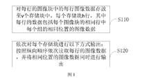
- FIG. 1 is a flowchart of a method for reading image data provided by the present disclosure
- FIG. 2 is a schematic diagram of a box block provided by the present disclosure
- FIG. 3 is still another flowchart of the image data reading method provided by the present disclosure.
- FIG. 4 is a schematic diagram showing the space development of an off-chip memory provided by the present disclosure.
- FIG. 5 is a schematic diagram of storing image data in a buffer area according to the present disclosure.
- FIG. 6 is a schematic diagram of counting of each counter provided by the present disclosure.
- FIG. 7 is a schematic diagram of a storage step in an image data reading method provided by the present disclosure.
- FIG. 8 is a schematic diagram of a reading step in an image data reading method provided by the present disclosure.
- FIG. 9 is a schematic diagram of efficiency comparison of an image data reading method provided by the present disclosure.
- FIG. 10 is a schematic diagram of an alignment of boxes of different resolution sizes provided by the present disclosure.
- FIG. 11 is a block schematic diagram of an electronic device configured to implement the above image data reading method provided by the present disclosure.
- Icon 100-electronic device; 110-readable storage medium; 120-processor; 200-image data reading device; 210-storage unit; 220-reading unit.
- the number of LED lamps that can be controlled by current LED driver chips is limited.
- One LED driver chip can only control LED lamps of row V and column H, and H is the largest data channel of LED driver chip, so it needs to drive chips through many LEDs.
- the same line of K parts is turned on at the same time.
- the same line of the K parts means that the Nth line of the K parts is simultaneously turned on, and the value of N ranges from 1-v.
- the first line of the K parts is turned on at the same time
- the second line of the K parts is turned on at the same time
- the third line of the K parts is turned on at the same time
- the LED driver chip needs to illuminate the k-line LED lamp at the same time
- the receiving card needs to synchronously send the same line of data to the LED driver chip.
- the horizontal direction it is impossible to cascade too many chips in the horizontal direction due to the limitation of the data clock of the LED driving chip.
- the period of the data clock DCLK of the LED driver chip is T, and the number of data bits per color channel of each pixel is B (commonly 16 bits).
- the time at which the main control chip reads the m image data to be transmitted of the m image blocks is t2;
- DCLK has an upper limit
- the number of chips cascaded has an upper limit
- the size of each image block of the box also has an upper limit.
- the number of image blocks can be increased, and the number of data groups can be increased, that is, the above m is increased.
- the image data reading efficiency of the external memory is too low, so that the t2 time is too large, thereby limiting the number of image blocks and the number of data sets, which limits the maximum number of data sets and the box that the receiving card can support to some extent. Resolution size.
- the present disclosure provides an image data reading method, apparatus, electronic device, and readable storage medium, so as to adopt a burst reading manner without changing the hardware read/write clock frequency or increasing the bit width. Shorten the reading time of the image data in the off-chip memory by the LED driver chip.
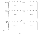
- the box is equally divided into L equal parts in the horizontal direction, thereby obtaining K*L image display areas, and displaying the K*L images.
- the areas are sequentially added with markers 1, 2, 3, ..., m.
- the image frame displayed on the box also includes K*L image blocks corresponding to the K*L image display areas, and the K*L image blocks are also marked as 1, respectively. 2, 3, ..., m.
- FIG. 2 it is a schematic diagram of the case where the box is folded in the horizontal direction and folded in the vertical direction by m/2.
- the image frame includes 2 image blocks in the horizontal direction and m/2 image blocks in the vertical direction.
- v and h are the number of rows and data channels configured for each LED driver chip
- n is the number of LED driver chips cascaded in the horizontal direction.
- each image block can be equally divided in the horizontal direction, and it is assumed that n image groups are equally divided by h.
- 1 to h are the first image group
- (h+1) to 2h are the second image group
- [(n-2)*h+1] to (n-1) *h is the n-1th image group
- [(n-1)*h+1] ⁇ n*h is the nth image group.
- the existing scheme for each of the m image blocks, it is necessary to sequentially read image data from the rightmost side to the leftmost side, for example, for each image block, first read the most of the nth image group.
- the right side is the data of the n*h position, and then reads the data of the (n-1)*h position in the n-1th image group until the data of the h position in the first image group is read; then returns to the most On the right side, the data of the n*h-1 position in the nth image group is read until the data of the h-1 position in the first image group is read; and so on until the first image group is read. 1 position data.
- the present disclosure can improve the above problem by using a burst image data reading method.
- FIG. 1 is a flowchart of a method for reading image data provided by the present disclosure.
- the image data reading method shown in FIG. 1 can be applied to an electronic device, which can be any device having an image processing function.
- the image data reading method shown in Fig. 1 includes the following steps.
- Step S110 storing, for each row of image data in each image block, into v storage blocks, each storage block h rows, wherein the data of each row includes the same position of each group in the same row of each image block.
- Image data
- step S120 each memory block is sequentially output in the following manner:
- the image data of each line is sequentially read in the vertical order, and the image data of the same position is simultaneously output.
- the electronic device may include an on-chip memory and an off-chip memory.
- each line of image data in the received image frame may be acquired through the on-chip memory buffer.
- the image data is arranged in a specific manner and stored in a memory block opened on the off-chip memory, so that when the data is read and output in the memory block, the discrete image data points on the box can be suddenly read, and the LED driving is shortened.
- the chip reads the image data in the off-chip memory and realizes the receiving card of the box capable of supporting the multi-data set large resolution at a low cost.
- step S110 can have different implementations.
- the electronic device when the electronic device includes a plurality of LED lamps arranged in an array, the plurality of LED lamps are configured to display the received image frames under the driving of the N LED driving chips, and each When the LED lamp driving chip is capable of driving the LED lamps of the v rows and the h columns, the off-chip memory may be opened with v memory blocks, and each memory block is divided into h packets, each packet being on the off-chip memory. Continuous address space.
- the electronic device is configured with an order of the v storage blocks and h packets in each storage block, which may be implemented by setting a number.
- step S110 may include the sub-steps as shown in FIG. 3:
- Step S31 receiving an image frame, wherein the image frame includes a plurality of image blocks, each image block includes v lines of image data, and each line of image data is divided into a plurality of data groups, each data group including h pixel data ;
- Step S32 for each image block included in the image frame, the pixel data in the jth position of each data group in the i-th row of each image block is written into the j-th data of the i-th storage space.
- the group wherein 1 ⁇ i ⁇ v, 1 ⁇ j ⁇ h.
- the image frame may include M image blocks, and each row of image data in each image block is divided into N data groups, and the number of data bits (bits) of each color channel of the pixels in the image frame is B, the size of each packet is at least M*N*3B(bit).
- step S32 can be implemented by the following sub-steps:
- a clock counter RCnt and a data channel counter GRPCnt may be disposed in the electronic device.
- the pixel data of the j-th position of each data group is sequentially read to obtain N pixel data, and the N pixel data is written.
- This step in the jth data group of the i th memory block can be implemented by the following substeps:
- the clock counter RCnt is cyclically counted, and each time counting, the pixel data of the GRPCnt+1 position in the RCnt+1 data group of the image data of the i-th row is read;
- the data channel counter GRPCnt is counted, and the currently read N pixel data is written in a burst manner to the i-th memory block.
- GRPCnt is in 1 group.
- the electronic device may allocate a corresponding storage interval Inter for each of the packets in the storage block, wherein the storage interval Inter can store at least one pixel in a data group, that is, Inter is greater than or equal to h.
- Inter 2 i ⁇ h, where i may take a minimum value that enables Inter to be greater than or equal to h.
- h pixels are stored in each storage interval.
- step S32 may further include the following sub-steps:
- the electronic device may be further provided with a line sweep counter BLKCnt.
- the value of BLKCnt is set to 1.
- the value of the BLKCnt is set to 1, and the image frame is written to the slice.
- the value of the BLKCnt reaches v.
- step S120 may include the sub-step of: after writing the image frame into the off-chip memory, performing image data of each line sequentially in a vertical order and images of the same position The step of simultaneously outputting data.
- sequentially reading the image data of each line in the vertical order and outputting the image data of the same position at the same time can be realized by the following substeps:
- the image data of the image frames stored in the respective storage blocks are sequentially read in a burst manner according to the sequence numbers of the storage blocks, wherein for each storage block, each data group is read in reverse order according to the sequence number of each data group. Pixel data in .
- step S110 can be implemented in the following manner, including:
- Step S201 storing image data of each line in the image block of each line in the following manner:
- the i-th image data of each group is sequentially extracted in order from left to right, corresponding to generating h image groups, and h image groups are grouped according to the sequence of generation.
- the off-chip memory includes v memory blocks, each memory block includes h rows; in each memory block, the j-th row group corresponding to the j-th row image data of the k-th row image block, and the k+1th The jth array group corresponding to the image data of the jth line of the line image block is adjacent, 1 ⁇ k ⁇ N-1;
- the first image data is first extracted from each group of the image data stored in the first line of the buffer area to form a first image group.
- the image group includes 2n.
- the first image data of each group in the group that is, the image group includes 2n image data, and similarly, the remaining second to hth image data are respectively selected to form the second to the hth image group respectively.
- the h image groups are vertically arranged in the order of generation, and the first array group corresponding to the image data of the first row is obtained, and the first array group is stored in the first storage block.
- the first row of image data in the first row of image blocks has been stored in the storage block, and the second row of image data in the first row of image blocks is further generated according to the above process, and the second array is generated and stored in the second storage block. And so on, until the v line image data in the first line image block are respectively put into v storage blocks, and then the second line image block is subjected to the above storage process until all the image data in the N line image block Are stored in v storage , And then the image data storage block v output.
- each memory block is sequentially output in the following manner: image data of each line is sequentially read in the vertical order, and image data of the same position is simultaneously output.
- the entire storage block is There are N*M*n/N image data in one row, that is, M*n image data;
- the M*n image data in the hth row of the first memory block is read from the right to the left, and the image data at the same position in the corresponding image block on the box is read, for example, M n first.
- *h Image data is simultaneously output in M data sets, and then M (n-1)*h image data are simultaneously output until M pieces of h image data are simultaneously output, and then M n*(h are output at this time.
- M image data is output through one pixel period in M data groups, that is, it takes N pixel periods to output the m*n image data of the hth line, and then according to the above process M*n image data in the h-1th line of the first memory block is output;
- the reading order of the storage block and the horizontal group is read from the first group to the vth group or the vth group to the first group, the first row to the hth row is read or the hth row is read to the first row
- the reading order in the above embodiment is only an example
- the image group has a preset space capacity, and the space capacity is calculated according to the following formula: P ⁇ m*3*n*B(bit);
- P is the spatial capacity
- m is the number of image blocks divided by the box
- n is the number of driving chips used for each color channel in each image block
- numeral 3 is represented as three-component RGB.
- the v-block space is opened in the off-chip memory, that is, v memory blocks are formed, each space is divided into h rows, and a continuous address space of the off-chip memory is used in the group, and each image grouping needs to meet a preset space capacity requirement. As shown in Figure 4.
- the method further includes:
- Step S122 the image data from the source end is read by ping pong through the two-line buffer area in the on-chip memory, and written into the memory block of the off-chip memory.
- each row of data of the acquired image frame may be alternately stored into the two-line buffer.
- step S122 can be implemented by the following steps, including:
- h is a data channel opened by each LED driver chip
- n represents each The number of drive chips used by each color channel of the image block.
- the number of folds in the horizontal direction of the box is not fixed.
- a 2-fold image block is taken as an example.
- the two-line buffer area in the on-chip memory operates simultaneously, when one line of the buffer area reads the second line of image data of the first line of image blocks, the other line of the buffer area simultaneously sets the first line of the first line of image blocks.
- the row image data is stored in the first storage block until all the v rows of image data of the first row of image blocks are read and written into the v storage blocks, and then the reading and writing operations of the second row of image blocks are started.
- the process is the same as the above embodiment, and will not be described here;
- Inter is a storage interval
- i is a minimum value that enables Inter to be greater than and equal to h
- h is the number of image data included in each packet.
- reading the f-th row image data in the image block of the e-th row, and storing the f-th row image data in the order of the left-to-right row in the buffer of the a-th row can be implemented by the following steps, including:
- Step 1 reading the g-th image data in the f-th row in the image block of the e-th row;
- Step 2 When the storage interval is not equal to 2 ⁇ i, the starting address of the image data of the g+1th group is crossed over 2 ⁇ ih image data addresses, and then stored in the buffer of the a-th row, where 1 ⁇ g ⁇ n-1.
- the counter RCnt represents a read clock counter
- GRPCnt represents an LED data channel counter
- BLKCnt represents a line scan counter.
- the number of LED chips used in the horizontal direction of the box is N, and the number of rows of each image block is V.
- RCnt counts from 0 to N-1 cycles.
- GRPCnt starts from 0 to the Inter-1 loop count.
- BLKCnt counts from 1 to V cycle.
- Rd_clk represents the read clock of the on-chip line buffer
- Sol represents the line mark of each line. Each line starts to clear the RCnt and GRPCnt, and each frame starts to set the BLKCnt.
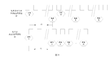
- FIG. 9 is a schematic diagram of an efficiency comparison of the image data reading method provided by the present disclosure.
- t1 represents the interval between the start of the read command and the return of the read data.
- the prior art solution has a time overhead of t1 when reading each LED pixel data.
- there is only one t1 time overhead for one burst read and if the maximum burst read by the external memory is supported, the read can be saved as much as possible. time;
- the number of data sets be m, and the data clock DCLK of the LED driver chip is f, and the resolution of each image block is V*H.
- the data bit width of each channel is N, and the image frame rate is F, then f>V*H*N*F;
- the prior art scheme has a low efficiency of reading from 10% to 40%, and has an effective bandwidth of 0.92 Gbps, corresponding to an external memory physical bandwidth of 2.3 Gbps to 9.2 Gbps.
- the image reading efficiency can reach 70% to 90%, and the external memory physical bandwidth is 1.0 Gbps to 1.3 Gbps.
- the bandwidth requirements for the external memory of the two schemes are 4.6 Gbps to 18.4 Gbps and 2.0 Gbps to 2.6 Gbps, respectively;
- the present disclosure can lower the bandwidth of the external memory, and can support the multi-data set large-resolution box receiving card with the lower performance master chip and the external memory.
- the main control chip includes an FPGA (Field Programmable Gate Array).
- the electronic device 100 may be, but not limited to, a personal computer (Personal Computer, PC), a notebook computer, a monitoring device, a server, and the like, which have image data reading and processing capabilities.
- PC Personal Computer
- PC Personal Computer
- notebook computer a monitoring device
- server a server
- the electronic device 100 includes an image data reading device 200, a readable storage medium 110, and a processor 120.
- the image data reading device 200 includes at least one operating system (OS) that can be stored in the readable storage medium 110 in the form of software or firmware or is solidified in the electronic device 100.
- the processor 120 is configured to execute an executable software module stored in the readable storage medium 110, for example, a software function module, a computer program, and the like included in the image data reading device 200.
- the image data reading device 200 may also be integrated in the operating system as part of the operating system.
- the image data reading device 200 includes:
- the storage unit 210 is configured to store, for each row of image data in each row of the image data, into v storage blocks, each storage block h rows, wherein the data of each row includes each group in the same row of each image block. Image data of the same location.
- the storage unit 210 is specifically configured to receive an image frame, wherein the image frame includes a plurality of image blocks, each image block includes v lines of image data, and each line of image data is divided into a plurality of data groups, each The data group includes h pixel data; for each image block included in the image frame, pixel data in the jth position of each data group in the i-th row of each image block is written into the i-th storage In the jth data group of the space, where 1 ⁇ i ⁇ v, 1 ⁇ j ⁇ h.
- the reading unit 220 is configured to sequentially output each of the memory blocks in the following manner: sequentially read image data of each line in a vertical order, and simultaneously output image data of the same position.
- the present disclosure provides an image data reading method, apparatus, electronic device, and readable storage medium, including storing image data of each line in each image block into v storage blocks, each storage block. h rows, wherein the data of each row includes image data of the same position of each group in the same row of each image block; sequentially outputting each memory block in the following manner: sequentially reading image data of each row in a vertical order, The image data of the same position is simultaneously outputted.
- the burst read mode is adopted to shorten the reading of the image data in the off-chip memory by the LED driver chip. Take time.
- each block of the flowchart or block diagram can represent a module, a program segment, or a portion of code that includes one or more of the Executable instructions. It should also be noted that, in some alternative implementations, the functions noted in the blocks may also occur in a different order than those illustrated in the drawings.
- each block of the block diagrams and/or flowcharts, and combinations of blocks in the block diagrams and/or flowcharts can be implemented in a dedicated hardware-based system that performs the specified function or function. Or it can be implemented by a combination of dedicated hardware and computer instructions.
- each functional module in various embodiments of the present disclosure may be integrated to form a separate part, or each module may exist separately, or two or more modules may be integrated to form a separate part.
- the term “comprising”, “including” or any other variants thereof is intended to encompass a non-exclusive inclusion, such that a process, method, article, or device comprising a Elements, but also other elements not explicitly listed, or elements that are inherent to such a process, method, item, or device.
- An element defined by the phrase “comprising a " does not exclude the presence of additional elements in the process, method, item, or device that comprises the element.
- the image data reading method, device, electronic device and readable storage medium provided by the present disclosure shorten the LED driving chip by using a burst reading mode without changing the hardware read/write clock frequency or increasing the bit width.
- the read time of the image data in the off-chip memory is shortened.
Landscapes
- Engineering & Computer Science (AREA)
- Theoretical Computer Science (AREA)
- Physics & Mathematics (AREA)
- General Physics & Mathematics (AREA)
- Computer Hardware Design (AREA)
- General Engineering & Computer Science (AREA)
- Human Computer Interaction (AREA)
- Control Of Indicators Other Than Cathode Ray Tubes (AREA)
- Image Input (AREA)
- Image Processing (AREA)
Abstract
公开了图像数据读取方法、装置、电子设备及可读存储介质,涉及LED图像显示技术领域,包括对每行的图像块中的每行图像数据存放至v个存储块中,每个存储块h行,其中每行的数据包括每个图像块的相同行中每个组的相同位置的图像数据;依次对每个存储块进行以下方式输出:按照纵向顺序依次读取每行的图像数据,并将相同位置的图像数据同时进行输出,在不改变硬件读写时钟频率或增大位宽的方式的基础上,采用突发读取方式,缩短LED驱动芯片对片外存储器中图像数据的读取时间。
Description
相关申请的交叉引用
本申请要求于2017年12月29日提交中国专利局的申请号为2017114982733,名称为“图像数据读取方法、装置、电子设备及可读存储介质”的中国专利申请的优先权,其全部内容通过引用结合在本申请中。
本公开涉及LED图像显示技术领域,尤其是涉及图像数据读取方法、装置、电子设备及可读存储介质。
一面小间距LED显示屏由个数不定的箱体拼接组成,一块箱体上贴满LED灯。箱体上插的接收卡控制行扫芯片和LED驱动芯片驱动LED灯的显示,箱体上显示的图像由源端发送卡逐行发送给箱体接收卡。由于接收卡主控芯片的片内存储器资源有限,一般情况下需将图像存储在片外存储器中。给LED驱动芯片传输图像数据时,逐个从图像的各个部分读取所需图像数据,然后再一起发送给LED驱动芯片。现有技术方案中,对片外存储器的读取效率太低,每次读取的图像数据太少,基本上不能突发读取,且为了保证数据传输不中断,多采用提高外部存储器读写时钟频率或增大位宽的方式,成本较高,限制较多。
发明内容
有鉴于此,本公开提供图像数据读取方法、装置、电子设备及可读存储介质。
第一方面,本公开提供了图像数据读取方法,应用于电子设备,所述方法包括:
对每行的图像块中的每行图像数据存放至v个存储块中,每个存储块h行,其中每行的数据包括每个图像块的相同行中每个组的相同位置的图像数据;
依次对每个所述存储块进行以下方式输出:
按照纵向顺序依次读取每行的图像数据,并将相同位置的图像数据同时进行输出。
可选地,所述电子设备包括开辟有v个存储块的片外存储器,每个存储块被划分为h个分组;对每行的图像块中的每行图像数据存放至v个存储块中,每个存储块h行,其中每行的数据包括每个图像块的相同行中每个组的相同位置的图像数据,包括:
接收图像帧,其中,所述图像帧包括多个图像块,每个图像块包括v行图像数据,每行图像数据被划分为多个数据组,每个数据组包括h个像素数据;
针对所述图像帧包括的各图像块,将所述各图像块的第i行中、处于各数据组的第j个位置的像素数据写入第i个存储空间的第j个数据组中,其中,1≤i≤v,1≤j≤h。
可选地,所述电子设备包括阵列设置的多个LED灯,所述多个LED灯配置成在N个LED驱动芯片的驱动下对接收到的图像帧进行显示,每个LED驱动芯片能够驱动v行h列的LED灯;
所述图像帧包括M个图像块,每个图像块中的每行图像数据被划分为N个数据组,所述图像帧中像素的每个颜色通道的数据比特数为B,则每个分组的空间大小至少达到M*N*3B比特。
可选地,所述电子设备包括片内存储器,所述片内存储器中开辟有缓存区;针对所述图像帧包括的各图像块,将所述各图像块的第i行中、处于各数据组的第j个位置的像素数据写入第i个存储块的第j个数据组中,包括:
按照从上至下的顺序依次获取所述图像帧的第i行图像数据,将获取到的所述第i行图像数据存储到所述缓存区中;
针对所述第i行图像数据的各数据组,依次读取所述各数据组的第j个位置的像素数据,得到N个像素数据,将所述N个像素数据写入到第i个存储块的第j个数据组中。
可选地,所述电子设备中设置有时钟计数器RCnt和数据通道计数器GRPCnt;针对所述第i行图像数据的各数据组,依次读取所述各数据组的第j个位置的像素数据,得到N个像素数据,将所述N个像素数据写入到第i个存储块的第j个数据组中,还包括:
在开始从所述缓存区读取所述第i行图像数据时,将所述时钟计数器RCnt和数据通道计数器GRPCnt清零;
对所述时钟计数器RCnt进行循环计数,在每次计数时,读取所述第i行图像数据的第RCnt+1个数据组中第GRPCnt+1个位置的像素数据;
当所述时钟计数器RCnt的值达到N-1时,对所述数据通道计数器GRPCnt进行计数,并将当前读取到的N个像素数据以突发的方式写入到第i个存储块的第GRPCnt+1个分组中。
可选地,所述电子设备为每个所述分组分配有对应的存储间隔Inter,该存储间隔的大小至少大于一个所述数据组的容量大小;
针对所述图像帧包括的各图像块,将所述各图像块的第i行中、处于各数据组的第j个位置的像素数据写入第i个存储块的第j个数据组中,还包括:
当所述时钟计数器RCnt的值达到N-1,且所述数据通道计数器GRPCnt的值达到Inter-1时,确定对所述第i行图像数据的读取完毕,开始从所述缓存区读取所述图像帧的下一行图像数据。
可选地,所述片内存储器中存储有两个缓存区;按照从上至下的顺序依次获取所述图像帧的第i行图像数据,将获取到的所述第i行图像数据存储到所述缓存区中,包括:
将获取到的各行图像数据交替地存储到所述两个缓存区中。
可选地,按照纵向顺序依次读取每行的图像数据,并将相同位置的图像数据同时进行输出,包括:
在将所述图像帧写入到所述片外存储器中之后,再执行按照纵向顺序依次读取每行的图像数据,并 将相同位置的图像数据同时进行输出的步骤。
可选地,按照纵向顺序依次读取每行的图像数据,并将相同位置的图像数据同时进行输出,包括:
以突发的方式、按照各存储块的序号依次读取各个存储块中存储的所述图像帧的图像数据,其中,针对每个存储块,按照各数据组的序号倒序读取每个数据组中的像素数据。
可选地,所述图像数据读取方法应用于划分为M个图像块的箱体,将所述M个图像块排列成N行,每个所述图像块包括v行图像数据,将每行的所述图像数据分成n组,每组包括h个图像数据,所述对每行的图像块中的每行图像数据存放至v个存储块中,每个存储块h行,其中每行的数据包括每个图像块的相同行中每个组的相同位置的图像数据包括:
对每行的图像块中的每行图像数据,进行以下方式存储:
从存储在缓存区的第j行图像数据中,按照从左至右的顺序依次将每组的第i个图像数据抽取出来,对应生成h个图像分组,将所述h个图像分组按照生成的先后顺序依次纵向排列,得到第j个排列组,并将所述第j个排列组存入第j个存储块中,其中,每个所述分组包括M*n/N个图像数据,1≤j≤v,1≤i≤h;
其中,片外存储器包括v个存储块,每个所述存储块包括h行;在每个所述存储块中,第k行图像块的第j行图像数据对应的第j个排列组,与第k+1行图像块的第j行图像数据对应的第j个排列组相邻,1≤k≤N-1。
可选地,所述方法还包括通过片内存储器中的两行缓存区以乒乓方式读取来自源端的所述图像数据,并写入所述片外存储器的存储块中。
可选地,所述通过片内存储器中的两行缓存区以乒乓方式读取来自源端的所述图像数据,并写入所述片外存储器的存储块中包括:
对每行的图像块中的每行图像数据,进行以下方式存储:
读取第e行的图像块中的第f行图像数据,将所述第f行图像数据按照从左至右的顺序存储在第a行缓存区中;
将已存储在第b行缓存区中的所述第f行图像数据存放至v个存储块中,1≤e≤N,1≤f≤v,a=1、b=2或a=2、b=1。
可选地,所述图像分组具有预设的空间容量,根据下式计算所述空间容量:
P≥m*3*n*B(bit);
其中,P为空间容量,m为箱体划分的所述图像块的个数,n为每个所述图像块中的每个颜色通道使用的驱动芯片个数。
可选地,所述缓存区包括至少一个存储间隔,其中,根据下式计算所述存储间隔:
Inter=2
i≥h;
其中,Inter为存储间隔,i为能够使Inter大于且等于h的最小值,h为每个分组中包含的图像数据的个数。
可选地,所述读取第e行的图像块中的第f行图像数据,将所述第f行图像数据按照从左至右的顺序存储在第a行缓存区中包括;
读取第e行的图像块中的第f行中的第g组图像数据;
当所述存储间隔不等于2^i时,将所述第g+1组图像数据的起始地址跨过2^i-h个图像数据地址,再存入第a行缓存区,其中,1≤g≤n-1。
第二方面,本公开还提供图像数据读取装置,包括:
存储单元,配置成对每行的图像块中的每行图像数据存放至v个存储块中,每个存储块h行,其中每行的数据包括每个图像块的相同行中每个组的相同位置的图像数据;
读取单元,配置成依次对每个所述存储块进行以下方式输出:按照纵向顺序依次读取每行的图像数据,并将相同位置的图像数据同时进行输出。
可选地,所述电子设备开辟有v个存储块的片外存储器,每个存储块被划分为h个分组;所述存储单元,具体配置成:
接收图像帧,其中,所述图像帧包括多个图像块,每个图像块包括v行图像数据,每行图像数据被划分为多个数据组,每个数据组包括h个像素数据;针对所述图像帧包括的各图像块,将所述各图像块的第i行中、处于各数据组的第j个位置的像素数据写入第i个存储空间的第j个数据组中,其中,1≤i≤v,1≤j≤h。
可选地,所述电子设备包括阵列设置的多个LED灯,所述多个LED灯配置成在N个LED驱动芯片的驱动下对接收到的图像帧进行显示,每个LED驱动芯片能够驱动v行h列的LED灯;
所述图像帧包括M个图像块,每个图像块中的每行图像数据被划分为N个数据组,所述图像帧中像素的每个颜色通道的数据比特数为B,则每个分组的空间大小至少达到M*N*3B比特。
第三方面,本公开还提供电子设备,包括:可读存储介质;处理器;以及图像数据读取装置,所述装置存储于所述可读存储介质中并包括由所述处理器执行的软件功能模块,所述装置包括:
存储单元,配置成对每行的图像块中的每行图像数据存放至v个存储块中,每个存储块h行,其中每行的数据包括每个图像块的相同行中每个组的相同位置的图像数据;
读取单元,配置成依次对每个所述存储块进行以下方式输出:按照纵向顺序依次读取每行的图像数据,并将相同位置的图像数据同时进行输出。
第四方面,本公开还提供一种可读存储介质,所述可读存储介质中存储有计算机程序,所述计算机程序被执行时实现权利要求1-7中任意一项所述的图像数据读取方法。
本公开的其他特征和优点将在随后的说明书中阐述,并且,部分地从说明书中变得显而易见,或者通过实施本公开而了解。本公开的目的和其他优点在说明书、权利要求书以及附图中所特别指出的结构来实现和获得。
为使本公开的上述目的、特征和优点能更明显易懂,下文特举较佳实施例,并配合所附附图,作详细说明如下。
为了更清楚地说明本公开的具体实施方式或现有技术中的技术方案,下面将对具体实施方式或现有技术描述中所需要使用的附图作简单地介绍,显而易见地,下面描述中的附图是本公开的一些实施方式,对于本领域普通技术人员来讲,在不付出创造性劳动的前提下,还可以根据这些附图获得其他的附图。
图1为本公开提供的一种图像数据读取方法的流程图;
图2为本公开提供的一种箱体分块示意图;
图3为本公开提供的图像数据读取方法的又一流程图;
图4为本公开提供的一种片外存储器的空间开辟示意图;
图5为本公开提供的一种图像数据在缓存区的存储方式示意图;
图6为本公开提供的各计数器的一种计数示意图;
图7为本公开提供的图像数据读取方法中的存储步骤示意图;
图8为本公开提供的图像数据读取方法中的读取步骤示意图;
图9为本公开提供的图像数据读取方法的效率比对示意图;
图10为本公开提供的不同分辨率大小的箱体的一种比对示意图;
图11为本公开提供的配置成实现上述图像数据读取方法的电子设备的方框示意图。
图标:100-电子设备;110-可读存储介质;120-处理器;200-图像数据读取装置;210-存储单元;220-读取单元。
为使本公开的目的、技术方案和优点更加清楚,下面将结合附图对本公开的技术方案进行清楚、完整地描述,显然,所描述的实施例是本公开的一部分实施例,而不是全部的实施例。基于本公开中的实施例,本领域普通技术人员在没有做出创造性劳动前提下所获得的所有其他实施例,都属于本公开保护的范围。
当前LED驱动芯片能够控制的LED灯的数量是有限的,一颗LED驱动芯片通常只能控制V行H列的LED灯,H为LED驱动芯片的最大数据通道,因而需要通过许多LED驱动芯片的级联来点亮一整个箱体LED灯。在垂直方向上,把箱体分成K个等分,每个部分的行数为v,v即为LED驱动芯片的行扫数。点亮LED灯时,K个部分的同一行同时导通。其中,K个部分的同一行是指K个部分的第N 行同时导通,N的取值范围为1-v。例如K个部分的第1行同时导通,K个部分的第2行同时导通,K个部分的第3行同时导通,以此类推。基于此,同一时刻LED驱动芯片需要同点亮k行LED灯,接收卡需要把同一行的数据同步发送给LED驱动芯片。在水平方向上,由于LED驱动芯片数据时钟的限制,水平方向上不可能级联太多的芯片。
假设LED驱动芯片的数据时钟DCLK的周期为T,每个像素的每个颜色通道数据比特数为B(常见是16bit)。LED驱动芯片是以串行方式接收数据,则一个像素发送的总时间(即像素周期)t1=B*T;
主控芯片读取m个图像块的m个待发送的图像数据的时间为t2;
要保证数据传输不中断,应该有t2<t1。
要满足t2<t1,可能的方法有:
(1)降低DCLK,增大t1;DCLK的下限是能保证一帧时间内能把一副画面数据传输完,所以DCLK不能无限制的降低。
(2)降低t2,提高外部存储器读写时钟频率或增大位宽,但这种方式会提高外部存储器和主控制器的成本;另外是想办法提高外部存储器的读取效率。
随着箱体的分辨率提高,像素点越多,从而需要将DCLK的周期设置得更小,t1也就越小;考虑到LED芯片的性能要求以及单板EMC(Electro Magnetic Compatibility,电磁兼容性)要求,DCLK具有上限,级联的芯片数具有上限,箱体每个图像块大小也具有上限。在此情况下,为了提高箱体LED分辨率,只能增大图像分块个数,增加数据组数,即增大上述的m。然而,外部存储器的图像数据读取效率太低,使得t2时间太大,从而限制图像块个数和数据组数,也就在一定程度上限制了接收卡可以支持的最多数据组数和箱体分辨率大小。
基于此,本公开提供一种图像数据读取方法、装置、电子设备及可读存储介质,以在不改变硬件读写时钟频率或增大位宽的方式的基础上,采用突发读取方式,缩短LED驱动芯片对片外存储器中图像数据的读取时间。
为便于对本实施例进行理解,首先对本公开所提供的图像数据读取方法进行详细介绍。
针对上述在垂直方向被划分为K个部分的箱体,在水平方向上把该箱体等分成L个等分,从而得到K*L个图像显示区域,并为所述K*L个图像显示区域依次添加标记1、2、3、...、m。对应地,在该箱体上显示的图像帧也包括与所述K*L个图像显示区域一一对应的K*L个图像块,所述K*L个图像块也分别被标记为1、2、3、...、m。如图2所示,为该箱体在水平方向上2折,垂直方向m/2折的情景示意图。对应地,针对在该箱体上显示的图像帧,该图像帧在水平方向上包括2个图像块,在垂直方向上包括m/2个图像块。其中v和h为每个LED驱动芯片配置的行扫个数和数据通道个数,n为水平方向上LED驱动芯片级联个数。
在上述场景中,一个图像帧被划分成m个图像块,需要m个数据组。每一个图像块的相同位置图 像数据需要同时发送,其中,相同位置是指水平方向和垂直方向上均相同的位置。例如,可以在水平方向上将每个图像块进行等分,假设以h为长度进行等分得到n个图像分组。其中,在水平方向上,1~h为第1个图像分组,(h+1)~2h为第2个图像分组,依次类推,[(n-2)*h+1]~(n-1)*h为第n-1个图像分组,[(n-1)*h+1]~n*h为第n个图像分组。
在现有方案中,针对m个图像块中的每一个,需要依次从最右侧往最左侧读取图像数据,例如,针对每个图像块,首先读取第n个图像分组中的最右侧即n*h位置的数据,然后读取第n-1个图像分组中(n-1)*h位置的数据,直至读取到第1个图像分组中h位置的数据;然后返回最右侧,读取第n个图像分组中n*h-1位置的数据,直至读取到第1个图像分组中h-1位置的数据;依次类推,直至读取到第1个图像分组中1位置的数据。
由此可见,在现有方案中,需要一个个数据进行读取和传输,效率较低,读取时间较长,本公开采用突发性图像数据读取方法就能够改善上述问题。
下面请参照图1,图1为本公开提供的图像数据读取方法流程图。图1所示的图像数据读取方法可以应用于电子设备,该电子设备可以是任意具有图像处理功能的设备。图1所示的图像数据读取方法包括以下步骤。
步骤S110,对每行的图像块中的每行图像数据存放至v个存储块中,每个存储块h行,其中每行的数据包括每个图像块的相同行中每个组的相同位置的图像数据。
步骤S120,依次对每个存储块进行以下方式输出:
按照纵向顺序依次读取每行的图像数据,并将相同位置的图像数据同时进行输出。
在本公开中,所述电子设备可以包括片内存储器和片外存储器,鉴于片内存储器的存储空间有限,可以先通过片内存储器缓存区获取接收到的图像帧中的每行图像数据,以特定方式排列图像数据,再存放在片外存储器上开辟的存储块中,使得在存储块中进行数据读取输出时,能够突发性地读取箱体上离散地图像数据点,缩短LED驱动芯片对片外存储器中图像数据的读取时间,并以较低的成本实现能支持多数据组大分辨率的箱体的接收卡。
在本公开中,步骤S110可以有不同的实现方式。在一种具体实施方式中,当所述电子设备包括阵列设置的多个LED灯,所述多个LED灯配置成在N个LED驱动芯片的驱动下对接收到的图像帧进行显示,且每个LED灯驱动芯片能够驱动v行h列的LED灯时,所述片外存储器可以开辟有v个存储块,每个存储块被划分为h个分组,每个分组为所述片外存储器上的连续地址空间。其中,所述电子设备为所述v个存储块及每个存储块中的h个分组设置有顺序,具体可以通过设置编号实现。
在此情况下,步骤S110可以包括如图3所示的子步骤:
步骤S31,接收图像帧,其中,所述图像帧包括多个图像块,每个图像块包括v行图像数据,每行 图像数据被划分为多个数据组,每个数据组包括h个像素数据;
步骤S32,针对所述图像帧包括的各图像块,将所述各图像块的第i行中、处于各数据组的第j个位置的像素数据写入第i个存储空间的第j个数据组中,其中,1≤i≤v,1≤j≤h。
其中,所述图像帧可以包括M个图像块,每个图像块中的每行图像数据被划分为N个数据组,所述图像帧中像素的每个颜色通道的数据比特(bit)数为B,则每个分组的空间大小至少达到M*N*3B(bit)。
可选地,步骤S32可以通过如下子步骤实现:
按照从上至下的顺序依次获取所述图像帧的第i行图像数据,将获取到的所述第i行图像数据存储到所述缓存区中;
针对所述第i行图像数据的各数据组,依次读取所述各数据组的第j个位置的像素数据,得到N个像素数据,将所述N个像素数据写入到第i个存储块的第j个数据组中。
可选地,在本公开中,所述电子设备中可以设置有时钟计数器RCnt和数据通道计数器GRPCnt。在此情况下,针对所述第i行图像数据的各数据组,依次读取所述各数据组的第j个位置的像素数据,得到N个像素数据,将所述N个像素数据写入到第i个存储块的第j个数据组中这一步骤,可以通过如下子步骤实现:
在开始从所述缓存区读取所述第i行图像数据时,将所述时钟计数器RCnt和数据通道计数器GRPCnt清零;
对所述时钟计数器RCnt进行循环计数,在每次计数时,读取所述第i行图像数据的第RCnt+1个数据组中第GRPCnt+1个位置的像素数据;
当所述时钟计数器RCnt的值达到N-1时,对所述数据通道计数器GRPCnt进行计数,并将当前读取到的N个像素数据以突发的方式写入到第i个存储块的第GRPCnt+1个分组中。
可选地,所述电子设备可以为存储块中的每个所述分组分配有对应的存储间隔Inter,其中,所述存储间隔Inter至少能够存储一个数据组中的像素,即,Inter大于或等于h。详细地,在本公开中,Inter=2
i≥h,其中,i可以取能够使Inter大于或等于h的最小值。在此情况下,每个存储间隔中存储有h个像素。
对应地,步骤S32还可以包括以下子步骤:
当所述时钟计数器RCnt的值达到N-1,且所述数据通道计数器GRPCnt的值达到Inter-1时,确定对所述第i行图像数据的读取完毕,开始从所述缓存区读取所述图像帧的下一行图像数据。
除此之外,所述电子设备中还可以设置有行扫计数器BLKCnt,在本公开中,BLKCnt的初始值为1,每当所述GRPCnt=Inter-1时,将所述BLKCnt的值累加1,直至所述BLKCnt的值达到v时,再将所述BLKCnt的值置为1。换言之,在开始对每一图像帧进行处理,例如开始将该图像帧的行图像数据存储到缓存区中时,将所述BLKCnt的值置为1,在将该图像帧写入到所述片外存储器时,所述BLKCnt的 值达到v。
在本公开中,步骤S120可以包括如下子步骤:在将所述图像帧写入到所述片外存储器中之后,再执行按照纵向顺序依次读取每行的图像数据,并将相同位置的图像数据同时进行输出的步骤。
详细地,按照纵向顺序依次读取每行的图像数据,并将相同位置的图像数据同时进行输出,可以通过如下子步骤实现:
以突发的方式、按照各存储块的序号依次读取各个存储块中存储的所述图像帧的图像数据,其中,针对每个存储块,按照各数据组的序号倒序读取每个数据组中的像素数据。
可选地,在另一种具体实施方式中,上述方法实施例,可以应用于被划分为M个图像块的箱体,将图像块排列成N行,每个图像块包括v行图像数据,将每行的图像数据分成n组,每组包括h个图像数据,根据上述图像数据读取方法实施例中,步骤S110可采用以下方式实现,包括:
步骤S201,对每行的图像块中的每行图像数据,进行以下方式存储:
从存储在缓存区的第j行图像数据中,按照从左至右的顺序依次将每组的第i个图像数据抽取出来,对应生成h个图像分组,将h个图像分组按照生成的先后顺序依次纵向排列,得到第j个排列组,并将第j个排列组存入第j个存储块中,其中,每个分组包括M*n/N个图像数据,1≤j≤v,1≤i≤h;
其中,片外存储器包括v个存储块,每个存储块包括h行;在每个存储块中,第k行图像块的第j行图像数据对应的第j个排列组,与第k+1行图像块的第j行图像数据对应的第j个排列组相邻,1≤k≤N-1;
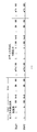
具体地,参照图7,先从存储在缓存区的第1行图像数据中的各个分组中,将第一个图像数据抽取出来,形成第一个图像分组,此时,这个图像分组中包括2n组中每组的第一个图像数据,即这个图像分组包括2n个图像数据,同理,分别挑选余下的第2个-第h个图像数据,分别形成第2个-第h个图像分组,再将这h个图像分组按照生成的先后顺序依次纵向排列,得到第一行图像数据对应的第一个排列组,并将第一个排列组存入第一个存储块中,此时箱体第一行图像块中的第一行图像数据已存入存储块,继续按照上述过程将第一行图像块中的第二行图像数据,生成第二个排列组,并存入第二存储块中,以此类推,直至第一行图像块中的v行图像数据都被分别放入v个存储块中,再将第二行图像块进行上述存储流程,直至N行图像块中所有图像数据都被存放到v个存储块中,再对v个存储块中的图像数据进行输出。
这里,依次对每个存储块进行以下方式输出:按照纵向顺序依次读取每行的图像数据,并将相同位置的图像数据同时进行输出。
其中,直至一帧图像写入完成后,即箱体全部的图像块中的所有图像数据都存入存储块中,从第一个存储块的第h行开始突发读取图像输出,读完h行后,读取h-1行,直到读完当前存储块;然后地址跳转到第二个存储块的第h行起始地址,直到循序读完所有的存储块,如图8所示;
可选地,当N行图像块全部写入时,由于每行图像块形成的排列组左右相邻,即第一个排列组在第二个排列组的左边或右边,此时整个存储块的一行中有N*M*n/N个图像数据,即M*n个图像数据;
这里,将第一个存储块的第h行中的M*n个图像数据按照从右至左的顺序,读取在箱体上相应图像块中相同位置的图像数据,如先将M个n*h图像数据同时在M个数据组中进行输出,接着将M个(n-1)*h图像数据同时输出,直至把M个h图像数据同时输出,此时再输出M个n*(h-1)图像数据至M个h-1图像数据,以此类推,即分别把M个图像块中的n个分组的相同位置的图像数据同时输出;
其中,通过图像数据在存储块中的上述排列方式以及将存储块中图像数据的输出形式,实现箱体图像块中互不相连、离散的图像数据的突发性读取和输出;
需要说明的是,M个图像数据在M个数据组中通过一个像素周期进行输出,即需经过N个像素周期,将第h行M*n个图像数据输出完毕,此时再按上述流程将第一个存储块的第h-1行中的M*n个图像数据进行输出;
其中,存储块和横向分组的读取顺序即由第一组到第v组读取或第v组到第一组,第一行到第h行读取或第h行到第一行读取,根据LED驱动芯片的需求和三分量RGB的排列顺序而决定,上述实施例中的读取顺序仅为一种示例;
进一步地,图像分组具有预设的空间容量,根据下式计算空间容量:P≥m*3*n*B(bit);
其中,P为空间容量,m为箱体划分的图像块的个数,n为每个图像块中的每个颜色通道使用的驱动芯片个数,数字3表征为三分量RGB。
这里,在片外存储器中开辟v块空间,即形成v个存储块,每块空间分成h行,组内使用片外存储器的连续地址空间,每个图像分组需要满足预设的空间容量要求,如图4所示。
进一步地,方法还包括:
步骤S122,通过片内存储器中的两行缓存区以乒乓方式读取来自源端的图像数据,并写入片外存储器的存储块中。
换言之,在实施时,可以将获取到的所述图像帧的各行数据交替地存储到所述两行缓存区中。
进一步地,步骤S122可用以下步骤实现,包括:
对每行的图像块中的每行图像数据,进行以下方式存储:
读取第e行的图像块中的第f行图像数据,将第f行图像数据按照从左至右的顺序存储在第a行缓存区中;
将已存储在第b行缓存区中的第f行图像数据存放至v个存储块中,1≤e≤N,1≤f≤v,a=1、b=2或a=2、b=1。
其中,在主控芯片内开辟两个行buffer(缓存区),交替存储源端发送的每行数据,如图5所示,其 中h为每个LED驱动芯片开通的数据通道,n表示每个图像块每个颜色通道使用的驱动芯片个数。箱体水平方向的折数不固定,图5中以2折图像块为例。
这里,片内存储器中的两行缓存区同时进行工作,当一行缓存区进行读取第一行图像块的第二行图像数据时,另一行缓存区同时在将第一行图像块的第一行图像数据存入第一个存储块中,直至将第一行图像块的v行图像数据全部读取写入v个存储块,再开始进行第二行图像块的读取写入工作,其过程与上述实施例相同,在此不再赘述;
进一步的,缓存区包括至少一个存储间隔,其中,根据下式计算存储间隔:Inter=2
i≥h;
其中,Inter为存储间隔,i为能够使Inter大于且等于h的最小值,h为每个分组中包含的图像数据的个数。
进一步地,读取第e行的图像块中的第f行图像数据,将第f行图像数据按照从左至右的顺序存储在第a行缓存区中可用以下步骤实现,包括:
步骤一,读取第e行的图像块中的第f行中的第g组图像数据;
步骤二,当存储间隔不等于2^i时,将第g+1组图像数据的起始地址跨过2^i-h个图像数据地址,再存入第a行缓存区,其中,1≤g≤n-1。
这里,当h不等于2^i时,下一段数据起始地址跨过(2^i-h)像素地址,图5所示的XX是跳过的空间;
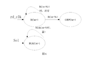
如图6所示,计数器RCnt表示读时钟计数器,GRPCnt表示LED数据通道计数器,BLKCnt表示行扫计数器。设箱体水平方向使用的LED芯片个数为N,每个图像块的行扫个数为V。RCnt从0开始到N-1循环计数。GRPCnt从0开始到Inter-1循环计数。BLKCnt从1开始到V循环计数。各个计数条件如图6所示。rd_clk表示片内行buffer的读时钟,Sol表示每行的行标志。每行开始对RCnt和GRPCnt做清零处理,每帧开始对BLKCnt做置1处理。
每个时刻,行buffer的读地址rd_addr={RCnt,GRPCnt},当Rcnt=N-1且GRPCnt=Inter-1时,当前行读取结束。每当Rcnt=N-1时,将读取的N个像素数据以突发的方式写入片外存储器第BLKCnt块、第GRPCnt+1组,组内的写入起始地是m*3*n*B(bit地址),如图7所示。
图9为本公开提供的图像数据读取方法的一种效率比对示意图。
其中,t1表示读命令发起到读返回数据的间隔时间。现有技术方案读取每一个LED像素数据时都有t1的时间开销,本公开中一次突发读取只有一个t1时间开销,如果以外部存储器支持的最大突发读,可以尽可能节省读取时间;
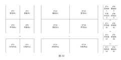
设数据组个数为m,LED驱动芯片数据时钟DCLK为f,设每个图像块的分辨率大小为V*H,如图10所示,每个通道数据位宽为N,图像帧率为F,则f>V*H*N*F;
LED驱动芯片传输数据的瞬时带宽BW=3*m*f*,设m=32,f=9.6MHz时,BW=0.92Gbps,即读LED 数据的瞬时带宽需要大于0.92Gbps;
现有技术方案读取的效率较低,在10%~40%,要达到0.92Gbps有效带宽,对应外部存储器物理带宽2.3Gbps~9.2Gbps。通过本公开提供的图像数据读取方法,对图像的读取效率可以达到70%~90%,对应外部存储器物理带宽1.0Gbps~1.3Gbps。
如图10所示,如果将左侧原始箱体的水平分辨率加大到2*H(每个图像块总像素增大一倍,f随之需增大一倍),即变为中间水平扩大箱体,纵向分辨率不变,则BW=3*32*9.6M*2=1.84Gbps。两种方案外部存储器所需的带宽要求分别是4.6Gbps~18.4Gbps和2.0Gbps~2.6Gbps;
如果箱体的水平分辨率不变,将左侧原始箱体的纵向分辨率加大到2*V(数据组m需增大一倍),即变为中间水平扩大箱体,BW=3*64*9.6M=1.84Gbps。两种方案外部存储器所需的带宽要求分别是4.6Gbps~18.4Gbps和2.0Gbps~2.6Gbps;
所以本公开对外部存储器带宽的要求可以更低,能够用较低性能的主控芯片和外部存储器支持多数据组大分辨率的箱体接收卡。这里,主控芯片包括FPGA(Field Programmable Gate Array,现场可编程门阵列)。
如图10所示,是本公开提供的用于实现所述图像分析方法的电子设备100的示意图。本实施例中,所述电子设备100可以是,但不限于,个人电脑(Personal Computer,PC)、笔记本电脑、监控设备、服务器等具备图像数据读取及处理能力的计算机设备。
所述电子设备100包括图像数据读取装置200、可读存储介质110以及处理器120。在本公开中,图像数据读取装置200包括至少一个可以软件或固件(Firmware)的形式存储于所述可读存储介质110中或固化在所述电子设备100的操作系统(Operating System,OS)中的软件功能模块。所述处理器120配置成执行所述可读存储介质110中存储的可执行软件模块,例如,所述图像数据读取装置200所包括的软件功能模块及计算机程序等。本实施例中,所述图像数据读取装置200也可以集成于所述操作系统中,作为所述操作系统的一部分。具体地,所述图像数据读取装置200包括:
存储单元210,配置成对每行的图像块中的每行图像数据存放至v个存储块中,每个存储块h行,其中每行的数据包括每个图像块的相同行中每个组的相同位置的图像数据。
在本公开中,存储单元210具体配置成接收图像帧,其中,所述图像帧包括多个图像块,每个图像块包括v行图像数据,每行图像数据被划分为多个数据组,每个数据组包括h个像素数据;针对所述图像帧包括的各图像块,将所述各图像块的第i行中、处于各数据组的第j个位置的像素数据写入第i个存储空间的第j个数据组中,其中,1≤i≤v,1≤j≤h。
读取单元220,配置成依次对每个所述存储块进行以下方式输出:按照纵向顺序依次读取每行的图像数据,并将相同位置的图像数据同时进行输出。
可以理解的是,本实施例中的各功能模块的具体操作方法可参照上述方法实施例中相应步骤的详细 描述,在此不再重复赘述。
综上所述,本公开提供了图像数据读取方法、装置、电子设备及可读存储介质,包括对每行的图像块中的每行图像数据存放至v个存储块中,每个存储块h行,其中每行的数据包括每个图像块的相同行中每个组的相同位置的图像数据;依次对每个存储块进行以下方式输出:按照纵向顺序依次读取每行的图像数据,并将相同位置的图像数据同时进行输出,在不改变硬件读写时钟频率或增大位宽的方式的基础上,采用突发读取方式,缩短LED驱动芯片对片外存储器中图像数据的读取时间。
在本公开所提供的实施例中,应该理解到,所揭露的装置和方法,也可以通过其它的方式实现。以上所描述的装置和方法实施例仅仅是示意性的,例如,附图中的流程图和框图显示了根据本公开的多个实施例的系统、方法和计算机程序产品的可能实现的体系架构、功能和操作。在这点上,流程图或框图中的每个方框可以代表一个模块、程序段或代码的一部分,所述模块、程序段或代码的一部分包含一个或多个用于实现规定的逻辑功能的可执行指令。也应当注意,在有些作为替换的实现方式中,方框中所标注的功能也可以以不同于附图中所标注的顺序发生。例如,两个连续的方框实际上可以基本并行地执行,它们有时也可以按相反的顺序执行,这依所涉及的功能而定。也要注意的是,框图和/或流程图中的每个方框、以及框图和/或流程图中的方框的组合,可以用执行规定的功能或动作的专用的基于硬件的系统来实现,或者可以用专用硬件与计算机指令的组合来实现。
另外,在本公开各个实施例中的各功能模块可以集成在一起形成一个独立的部分,也可以是各个模块单独存在,也可以两个或两个以上模块集成形成一个独立的部分。需要说明的是,在本文中,术语"包括"、"包含"或者其任何其它变体意在涵盖非排它性的包含,从而使得包括一系列要素的过程、方法、物品或者设备不仅包括那些要素,而且还包括没有明确列出的其它要素,或者是还包括为这种过程、方法、物品或者设备所固有的要素。在没有更多限制的情况下,由语句"包括一个……"限定的要素,并不排除在包括所述要素的过程、方法、物品或者设备中还存在另外的相同要素。
对于本领域技术人员而言,显然本公开不限于上述示范性实施例的细节,而且在不背离本公开的精神或基本特征的情况下,能够以其它的具体形式实现本公开。因此,无论从哪一点来看,均应将实施例看作是示范性的,而且是非限制性的,本公开的范围由所附权利要求而不是上述说明限定,因此旨在将落在权利要求的等同要件的含义和范围内的所有变化囊括在本公开内。不应将权利要求中的任何附图标记视为限制所涉及的权利要求。
本公开提供的图像数据读取方法、装置、电子设备及可读存储介质,在不改变硬件读写时钟频率或增大位宽的方式的基础上,采用突发读取方式,缩短LED驱动芯片对片外存储器中图像数据的读取时间。
Claims (20)
- 一种图像数据读取方法,其特征在于,应用于电子设备,所述方法包括:对每行的图像块中的每行图像数据存放至v个存储块中,每个存储块h行,其中每行的数据包括每个图像块的相同行中每个组的相同位置的图像数据;依次对每个所述存储块进行以下方式输出:按照纵向顺序依次读取每行的图像数据,并将相同位置的图像数据同时进行输出。
- 根据权利要求1所述的图像数据读取方法,其特征在于,所述电子设备包括开辟有v个存储块的片外存储器,每个存储块被划分为h个分组;对每行的图像块中的每行图像数据存放至v个存储块中,每个存储块h行,其中每行的数据包括每个图像块的相同行中每个组的相同位置的图像数据,包括:接收图像帧,其中,所述图像帧包括多个图像块,每个图像块包括v行图像数据,每行图像数据被划分为多个数据组,每个数据组包括h个像素数据;针对所述图像帧包括的各图像块,将所述各图像块的第i行中、处于各数据组的第j个位置的像素数据写入第i个存储空间的第j个数据组中,其中,1≤i≤v,1≤j≤h。
- 根据权利要求2所述的图像数据读取方法,其特征在于,所述电子设备包括阵列设置的多个LED灯,所述多个LED灯配置成在N个LED驱动芯片的驱动下对接收到的图像帧进行显示,每个LED驱动芯片能够驱动v行h列的LED灯;所述图像帧包括M个图像块,每个图像块中的每行图像数据被划分为N个数据组,所述图像帧中像素的每个颜色通道的数据比特数为B,则每个分组的空间大小至少达到M*N*3B比特。
- 根据权利要求2或3所述的图像数据读取方法,其特征在于,所述电子设备包括片内存储器,所述片内存储器中开辟有缓存区;针对所述图像帧包括的各图像块,将所述各图像块的第i行中、处于各数据组的第j个位置的像素数据写入第i个存储块的第j个数据组中,包括:按照从上至下的顺序依次获取所述图像帧的第i行图像数据,将获取到的所述第i行图像数据存储到所述缓存区中;针对所述第i行图像数据的各数据组,依次读取所述各数据组的第j个位置的像素数据,得到N个像素数据,将所述N个像素数据写入到第i个存储块的第j个数据组中。
- 根据权利要求4所述的图像数据读取方法,其特征在于,所述电子设备中设置有时钟计数器RCnt和数据通道计数器GRPCnt;针对所述第i行图像数据的各数据组,依次读取所述各数据组的第j个位置的像素数据,得到N个像素数据,将所述N个像素数据写入到第i个存储块的第j个数据组中,包括:在开始从所述缓存区读取所述第i行图像数据时,将所述时钟计数器RCnt和数据通道计数器GRPCnt清零;对所述时钟计数器RCnt进行循环计数,在每次计数时,读取所述第i行图像数据的第RCnt+1个数 据组中第GRPCnt+1个位置的像素数据;当所述时钟计数器RCnt的值达到N-1时,对所述数据通道计数器GRPCnt进行计数,并将当前读取到的N个像素数据以突发的方式写入到第i个存储块的第GRPCnt+1个分组中。
- 根据权利要求5所述的图像数据读取方法,其特征在于,所述电子设备为每个所述分组分配有对应的存储间隔Inter,该存储间隔Inter至少能够存储一个数据组中的像素;针对所述图像帧包括的各图像块,将所述各图像块的第i行中、处于各数据组的第j个位置的像素数据写入第i个存储块的第j个数据组中,还包括:当所述时钟计数器RCnt的值达到N-1,且所述数据通道计数器GRPCnt的值达到Inter-1时,确定对所述第i行图像数据的读取完毕,开始从所述缓存区读取所述图像帧的下一行图像数据。
- 根据权利要求4-6中任一项所述的图像数据读取方法,其特征在于,所述片内存储器中存储有两个缓存区;按照从上至下的顺序依次获取所述图像帧的第i行图像数据,将获取到的所述第i行图像数据存储到所述缓存区中,包括:将获取到的各行图像数据交替地存储到所述两个缓存区中。
- 根据权利要求2-7中任一项所述的图像数据读取方法,其特征在于,按照纵向顺序依次读取每行的图像数据,并将相同位置的图像数据同时进行输出,包括:在将所述图像帧写入到所述片外存储器中之后,再执行按照纵向顺序依次读取每行的图像数据,并将相同位置的图像数据同时进行输出的步骤。
- 根据权利要求8所述的图像数据读取方法,其特征在于,按照纵向顺序依次读取每行的图像数据,并将相同位置的图像数据同时进行输出,包括:以突发的方式、按照各存储块的序号依次读取各个存储块中存储的所述图像帧的图像数据,其中,针对每个存储块,按照各数据组的序号倒序读取每个数据组中的像素数据。
- 根据权利要求1所述的图像数据读取方法,其特征在于,应用于被划分为M个图像块的箱体,将所述M个图像块排列成N行,每个所述图像块包括v行图像数据,将每行的所述图像数据分成n组,每组包括h个图像数据,所述对每行的图像块中的每行图像数据存放至v个存储块中,每个存储块h行,其中每行的数据包括每个图像块的相同行中每个组的相同位置的图像数据包括:对每行的图像块中的每行图像数据,进行以下方式存储:从存储在缓存区的第j行图像数据中,按照从左至右的顺序依次将每组的第i个图像数据抽取出来,对应生成h个图像分组,将所述h个图像分组按照生成的先后顺序依次纵向排列,得到第j个排列组,并将所述第j个排列组存入第j个存储块中,其中,每个所述分组包括M*n/N个图像数据,1≤j≤v,1≤i≤h;其中,片外存储器包括v个存储块,每个所述存储块包括h行;在每个所述存储块中,第k行图像 块的第j行图像数据对应的第j个排列组,与第k+1行图像块的第j行图像数据对应的第j个排列组相邻,1≤k≤N-1。
- 根据权利要求10所述的图像数据读取方法,其特征在于,所述方法还包括通过片内存储器中的两行缓存区以乒乓方式读取来自源端的所述图像数据,并写入所述片外存储器的存储块中。
- 根据权利要求11所述的图像数据读取方法,其特征在于,所述通过片内存储器中的两行缓存区以乒乓方式读取来自源端的所述图像数据,并写入所述片外存储器的存储块中包括:对每行的图像块中的每行图像数据,进行以下方式存储:读取第e行的图像块中的第f行图像数据,将所述第f行图像数据按照从左至右的顺序存储在第a行缓存区中;将已存储在第b行缓存区中的所述第f行图像数据存放至v个存储块中,1≤e≤N,1≤f≤v,a=1、b=2或a=2、b=1。
- 根据权利要求10所述的图像数据读取方法,其特征在于,所述图像分组具有预设的空间容量,根据下式计算所述空间容量:P≥m*3*n*B(bit);其中,P为空间容量,m为箱体划分的所述图像块的个数,n为每个所述图像块中的每个颜色通道使用的驱动芯片个数。
- 根据权利要求12所述的图像数据读取方法,其特征在于,所述缓存区包括至少一个存储间隔,其中,根据下式计算所述存储间隔:Inter=2 i≥h;其中,Inter为存储间隔,i为能够使Inter大于或等于h的最小值,h为每个分组中包含的图像数据的个数。
- 根据权利要求14所述的图像数据读取方法,其特征在于,所述读取第e行的图像块中的第f行图像数据,将所述第f行图像数据按照从左至右的顺序存储在第a行缓存区中包括;读取第e行的图像块中的第f行中的第g组图像数据;当所述存储间隔不等于2 i时,将所述第g+1组图像数据的起始地址跨过2 i-h个图像数据地址,再存入第a行缓存区,其中,1≤g≤n-1。
- 一种图像数据读取装置,其特征在于,包括:存储单元,用于对每行的图像块中的每行图像数据存放至v个存储块中,每个存储块h行,其中每行的数据包括每个图像块的相同行中每个组的相同位置的图像数据;读取单元,用于依次对每个所述存储块进行以下方式输出:按照纵向顺序依次读取每行的图像数据, 并将相同位置的图像数据同时进行输出。
- 根据权利要求16所述的图像数据读取装置,其特征在于,应用于电子设备,所述电子设备开辟有v个存储块的片外存储器,每个存储块被划分为h个分组;所述存储单元,具体配置成:接收图像帧,其中,所述图像帧包括多个图像块,每个图像块包括v行图像数据,每行图像数据被划分为多个数据组,每个数据组包括h个像素数据;针对所述图像帧包括的各图像块,将所述各图像块的第i行中、处于各数据组的第j个位置的像素数据写入第i个存储空间的第j个数据组中,其中,1≤i≤v,1≤j≤h。
- 根据权利要求17所述的图像数据读取装置,其特征在于,所述电子设备包括阵列设置的多个LED灯,所述多个LED灯配置成在N个LED驱动芯片的驱动下对接收到的图像帧进行显示,每个LED驱动芯片能够驱动v行h列的LED灯;所述图像帧包括M个图像块,每个图像块中的每行图像数据被划分为N个数据组,所述图像帧中像素的每个颜色通道的数据比特数为B,则每个分组的空间大小至少达到M*N*3B比特。
- 一种电子设备,其特征在于,所述电子设备包括:可读存储介质;处理器;以及图像数据读取装置,所述装置存储于所述可读存储介质中并包括由所述处理器执行的软件功能模块,所述装置包括:存储单元,配置成对每行的图像块中的每行图像数据存放至v个存储块中,每个存储块h行,其中每行的数据包括每个图像块的相同行中每个组的相同位置的图像数据;读取单元,配置成依次对每个所述存储块进行以下方式输出:按照纵向顺序依次读取每行的图像数据,并将相同位置的图像数据同时进行输出。
- 一种可读存储介质,其特征在于,所述可读存储介质中存储有计算机程序,所述计算机程序被执行时实现权利要求1-15中任意一项所述的图像数据读取方法。
Priority Applications (4)
| Application Number | Priority Date | Filing Date | Title |
|---|---|---|---|
| US16/954,489 US11270675B2 (en) | 2017-12-29 | 2018-09-10 | Burst image data reading method and apparatus, electronic device, and readable storage medium |
| ES18894854T ES3055478T3 (en) | 2017-12-29 | 2018-09-10 | Image data reading method and apparatus, electronic device, and readable storage medium |
| EP18894854.1A EP3734582B1 (en) | 2017-12-29 | 2018-09-10 | Image data reading method and apparatus, electronic device, and readable storage medium |
| PL18894854.1T PL3734582T3 (pl) | 2017-12-29 | 2018-09-10 | Sposób oraz urządzenie do odczytu danych obrazu, urządzenie elektroniczne oraz czytelny nośnik pamięci masowej |
Applications Claiming Priority (2)
| Application Number | Priority Date | Filing Date | Title |
|---|---|---|---|
| CN201711498273.3 | 2017-12-29 | ||
| CN201711498273.3A CN109992234B (zh) | 2017-12-29 | 2017-12-29 | 图像数据读取方法、装置、电子设备及可读存储介质 |
Publications (1)
| Publication Number | Publication Date |
|---|---|
| WO2019128306A1 true WO2019128306A1 (zh) | 2019-07-04 |
Family
ID=67062983
Family Applications (1)
| Application Number | Title | Priority Date | Filing Date |
|---|---|---|---|
| PCT/CN2018/104861 Ceased WO2019128306A1 (zh) | 2017-12-29 | 2018-09-10 | 图像数据读取方法、装置、电子设备及可读存储介质 |
Country Status (6)
| Country | Link |
|---|---|
| US (1) | US11270675B2 (zh) |
| EP (1) | EP3734582B1 (zh) |
| CN (1) | CN109992234B (zh) |
| ES (1) | ES3055478T3 (zh) |
| PL (1) | PL3734582T3 (zh) |
| WO (1) | WO2019128306A1 (zh) |
Cited By (1)
| Publication number | Priority date | Publication date | Assignee | Title |
|---|---|---|---|---|
| CN114422807A (zh) * | 2022-03-28 | 2022-04-29 | 麒麟软件有限公司 | 一种基于Spice协议的传输优化方法 |
Families Citing this family (10)
| Publication number | Priority date | Publication date | Assignee | Title |
|---|---|---|---|---|
| JP6958526B2 (ja) * | 2018-09-26 | 2021-11-02 | 株式会社デンソー | 画像処理装置及び画像表示システム |
| CN110580273B (zh) * | 2019-09-11 | 2023-02-28 | 四川易利数字城市科技有限公司 | 地图gis数据处理存储方法、装置、可读存储介质 |
| CN110610679B (zh) * | 2019-09-26 | 2021-04-16 | 京东方科技集团股份有限公司 | 一种数据处理方法及装置 |
| CN112529016A (zh) * | 2020-12-21 | 2021-03-19 | 浙江欣奕华智能科技有限公司 | 一种图像中特征点的提取方法及提取装置 |
| CN113672172B (zh) * | 2021-07-29 | 2025-04-25 | 浙江大华技术股份有限公司 | 应用于led显示控制系统的数据交互方法以及接收卡 |
| CN114022345B (zh) * | 2021-11-12 | 2025-09-16 | 中国科学院长春光学精密机械与物理研究所 | 一种多通道大面阵图像的动态开窗方法及装置 |
| CN116417047A (zh) * | 2021-12-31 | 2023-07-11 | 西安钛铂锶电子科技有限公司 | 一种数据读取的方法及数据读取设备 |
| TWI797961B (zh) * | 2022-01-17 | 2023-04-01 | 大陸商北京集創北方科技股份有限公司 | 顯示數據之儲存和顯示方法及利用其之顯示裝置和資訊處理裝置 |
| CN114565501B (zh) * | 2022-02-21 | 2024-03-22 | 格兰菲智能科技有限公司 | 用于卷积运算的数据加载方法及其装置 |
| CN115113424B (zh) * | 2022-06-24 | 2024-06-04 | 利亚德光电股份有限公司 | 数据存取方法、装置、非易失性存储介质及图像处理设备 |
Citations (6)
| Publication number | Priority date | Publication date | Assignee | Title |
|---|---|---|---|---|
| CN1668092A (zh) * | 2004-03-09 | 2005-09-14 | 北京中星微电子有限公司 | 一种节省存储空间的存储处理方法 |
| CN101236740A (zh) * | 2008-02-25 | 2008-08-06 | 华为技术有限公司 | 一种显示数据的传输方法及装置 |
| CN101511021A (zh) * | 2009-03-24 | 2009-08-19 | 北京中星微电子有限公司 | 在sdram中存取图像数据的方法 |
| CN102163404A (zh) * | 2011-04-26 | 2011-08-24 | 西安交通大学 | 基于sdram的大屏幕led显示控制装置及方法 |
| US20160218739A1 (en) * | 2014-02-17 | 2016-07-28 | Mediatek Inc. | Data access methods and data access devices utilizing the same |
| CN106101712A (zh) * | 2016-06-13 | 2016-11-09 | 浙江大华技术股份有限公司 | 一种视频流数据的处理方法及装置 |
Family Cites Families (13)
| Publication number | Priority date | Publication date | Assignee | Title |
|---|---|---|---|---|
| US5745118A (en) * | 1995-06-06 | 1998-04-28 | Hewlett-Packard Company | 3D bypass for download of textures |
| US6411302B1 (en) * | 1999-01-06 | 2002-06-25 | Concise Multimedia And Communications Inc. | Method and apparatus for addressing multiple frame buffers |
| TW582015B (en) * | 2000-06-30 | 2004-04-01 | Nichia Corp | Display unit communication system, communication method, display unit, communication circuit and terminal adapter |
| US6999091B2 (en) * | 2001-12-28 | 2006-02-14 | Intel Corporation | Dual memory channel interleaving for graphics and video |
| EP1479066A2 (en) * | 2002-02-21 | 2004-11-24 | Koninklijke Philips Electronics N.V. | Method of storing data−elements |
| JP2008052522A (ja) * | 2006-08-25 | 2008-03-06 | Fujitsu Ltd | 画像データアクセス装置及び画像データアクセス方法 |
| KR100817057B1 (ko) | 2006-08-30 | 2008-03-26 | 삼성전자주식회사 | 동일한 픽셀 데이터 그룹에 포함되는 픽셀 데이터들을메모리의 동일한 뱅크 어드레스로 매핑하는 매핑 방법 및비디오 시스템 |
| JP5357399B2 (ja) * | 2007-03-09 | 2013-12-04 | 株式会社ジャパンディスプレイ | 表示装置 |
| KR101467935B1 (ko) | 2007-12-11 | 2014-12-03 | 삼성전자주식회사 | 디스플레이 장치 및 그 제어방법 |
| US7916572B1 (en) * | 2008-07-28 | 2011-03-29 | Altera Corporation | Memory with addressable subword support |
| WO2013094259A1 (ja) | 2011-12-20 | 2013-06-27 | シャープ株式会社 | 表示装置 |
| CN104378574B (zh) * | 2014-12-01 | 2017-11-24 | 北京理工大学 | 基于SoPC的VGA图像采集与压缩存储装置 |
| CN105741237B (zh) * | 2016-01-26 | 2019-03-26 | 南京铁道职业技术学院 | 一种基于fpga图像翻转的硬件实现方法 |
-
2017
- 2017-12-29 CN CN201711498273.3A patent/CN109992234B/zh active Active
-
2018
- 2018-09-10 ES ES18894854T patent/ES3055478T3/es active Active
- 2018-09-10 EP EP18894854.1A patent/EP3734582B1/en active Active
- 2018-09-10 US US16/954,489 patent/US11270675B2/en active Active
- 2018-09-10 WO PCT/CN2018/104861 patent/WO2019128306A1/zh not_active Ceased
- 2018-09-10 PL PL18894854.1T patent/PL3734582T3/pl unknown
Patent Citations (6)
| Publication number | Priority date | Publication date | Assignee | Title |
|---|---|---|---|---|
| CN1668092A (zh) * | 2004-03-09 | 2005-09-14 | 北京中星微电子有限公司 | 一种节省存储空间的存储处理方法 |
| CN101236740A (zh) * | 2008-02-25 | 2008-08-06 | 华为技术有限公司 | 一种显示数据的传输方法及装置 |
| CN101511021A (zh) * | 2009-03-24 | 2009-08-19 | 北京中星微电子有限公司 | 在sdram中存取图像数据的方法 |
| CN102163404A (zh) * | 2011-04-26 | 2011-08-24 | 西安交通大学 | 基于sdram的大屏幕led显示控制装置及方法 |
| US20160218739A1 (en) * | 2014-02-17 | 2016-07-28 | Mediatek Inc. | Data access methods and data access devices utilizing the same |
| CN106101712A (zh) * | 2016-06-13 | 2016-11-09 | 浙江大华技术股份有限公司 | 一种视频流数据的处理方法及装置 |
Non-Patent Citations (1)
| Title |
|---|
| See also references of EP3734582A4 * |
Cited By (1)
| Publication number | Priority date | Publication date | Assignee | Title |
|---|---|---|---|---|
| CN114422807A (zh) * | 2022-03-28 | 2022-04-29 | 麒麟软件有限公司 | 一种基于Spice协议的传输优化方法 |
Also Published As
| Publication number | Publication date |
|---|---|
| EP3734582A4 (en) | 2021-08-25 |
| CN109992234A (zh) | 2019-07-09 |
| EP3734582A1 (en) | 2020-11-04 |
| EP3734582C0 (en) | 2025-11-19 |
| PL3734582T3 (pl) | 2026-03-30 |
| EP3734582B1 (en) | 2025-11-19 |
| US11270675B2 (en) | 2022-03-08 |
| CN109992234B (zh) | 2020-11-17 |
| ES3055478T3 (en) | 2026-02-12 |
| US20210142767A1 (en) | 2021-05-13 |
Similar Documents
| Publication | Publication Date | Title |
|---|---|---|
| WO2019128306A1 (zh) | 图像数据读取方法、装置、电子设备及可读存储介质 | |
| JP6538179B2 (ja) | 表示制御装置、表示装置、表示制御装置の制御方法、および制御プログラム | |
| JP6363353B2 (ja) | 表示デバイスのドライバ | |
| CN115132133A (zh) | 像素倍增显示屏的数据传输系统、控制系统、方法和装置 | |
| CN110570793B (zh) | 一种适配不同类型显示屏的测试方法、装置及终端设备 | |
| TWI415475B (zh) | 圖像處理裝置及圖像處理方法 | |
| US10620899B2 (en) | Video display device and video data transmission method | |
| CN209845158U (zh) | 一种全激光投影的三级视频信息传输系统 | |
| CN105549943B (zh) | 显示驱动方法和显示系统 | |
| KR20080036844A (ko) | 타이밍 컨트롤러 및 이를 포함하는 액정 표시 장치 | |
| CN114428753B (zh) | 显示数据传输装置和显示数据传输方法 | |
| CN113205785B (zh) | 帧显示信号同步方法、显示装置、电子设备及存储介质 | |
| US10019931B2 (en) | Electronic paper display apparatus and driving method thereof | |
| CN118692352A (zh) | 控制信号分时复用的显示系统和方法 | |
| CN214377606U (zh) | 一种Mini-LED显示屏拼接显示驱动系统 | |
| CN102419956A (zh) | 一种连续图像播放led显示屏驱动芯片 | |
| US10262624B2 (en) | Separating a compressed stream into multiple streams | |
| JP2013195963A (ja) | 画像処理装置、集積回路装置及び画像表示システム | |
| US12511704B2 (en) | Method for performing tile to raster (T2R) conversion in deep learning hardware accelerator | |
| CN110796982A (zh) | 影像显示的驱动方法、驱动芯片、驱动装置以及显示装置 | |
| CN110336988B (zh) | 一种全激光投影的三级视频信息传输系统 | |
| CN114449183B (zh) | 影像处理芯片与影像处理方法 | |
| CN103366669B (zh) | 一种控制显示驱动时序的方法及播放设备 | |
| CN119068823A (zh) | 时序控制和行列驱动电路、驱动方法及显示装置 | |
| US8564603B2 (en) | Apparatus for controlling memory device and related method |
Legal Events
| Date | Code | Title | Description |
|---|---|---|---|
| 121 | Ep: the epo has been informed by wipo that ep was designated in this application |
Ref document number: 18894854 Country of ref document: EP Kind code of ref document: A1 |
|
| NENP | Non-entry into the national phase |
Ref country code: DE |
|
| ENP | Entry into the national phase |
Ref document number: 2018894854 Country of ref document: EP Effective date: 20200729 |
|
| WWG | Wipo information: grant in national office |
Ref document number: 2018894854 Country of ref document: EP |