WO2019131804A1 - Module optique et procédé d'assemblage de celui-ci - Google Patents
Module optique et procédé d'assemblage de celui-ci Download PDFInfo
- Publication number
- WO2019131804A1 WO2019131804A1 PCT/JP2018/047950 JP2018047950W WO2019131804A1 WO 2019131804 A1 WO2019131804 A1 WO 2019131804A1 JP 2018047950 W JP2018047950 W JP 2018047950W WO 2019131804 A1 WO2019131804 A1 WO 2019131804A1
- Authority
- WO
- WIPO (PCT)
- Prior art keywords
- output
- input
- lens
- semiconductor modulator
- lens system
- Prior art date
- Legal status (The legal status is an assumption and is not a legal conclusion. Google has not performed a legal analysis and makes no representation as to the accuracy of the status listed.)
- Ceased
Links
Images






Classifications
-
- G—PHYSICS
- G02—OPTICS
- G02F—OPTICAL DEVICES OR ARRANGEMENTS FOR THE CONTROL OF LIGHT BY MODIFICATION OF THE OPTICAL PROPERTIES OF THE MEDIA OF THE ELEMENTS INVOLVED THEREIN; NON-LINEAR OPTICS; FREQUENCY-CHANGING OF LIGHT; OPTICAL LOGIC ELEMENTS; OPTICAL ANALOGUE/DIGITAL CONVERTERS
- G02F1/00—Devices or arrangements for the control of the intensity, colour, phase, polarisation or direction of light arriving from an independent light source, e.g. switching, gating or modulating; Non-linear optics
- G02F1/01—Devices or arrangements for the control of the intensity, colour, phase, polarisation or direction of light arriving from an independent light source, e.g. switching, gating or modulating; Non-linear optics for the control of the intensity, phase, polarisation or colour
- G02F1/21—Devices or arrangements for the control of the intensity, colour, phase, polarisation or direction of light arriving from an independent light source, e.g. switching, gating or modulating; Non-linear optics for the control of the intensity, phase, polarisation or colour by interference
- G02F1/225—Devices or arrangements for the control of the intensity, colour, phase, polarisation or direction of light arriving from an independent light source, e.g. switching, gating or modulating; Non-linear optics for the control of the intensity, phase, polarisation or colour by interference in an optical waveguide structure
- G02F1/2257—Devices or arrangements for the control of the intensity, colour, phase, polarisation or direction of light arriving from an independent light source, e.g. switching, gating or modulating; Non-linear optics for the control of the intensity, phase, polarisation or colour by interference in an optical waveguide structure the optical waveguides being made of semiconducting material
-
- G—PHYSICS
- G02—OPTICS
- G02F—OPTICAL DEVICES OR ARRANGEMENTS FOR THE CONTROL OF LIGHT BY MODIFICATION OF THE OPTICAL PROPERTIES OF THE MEDIA OF THE ELEMENTS INVOLVED THEREIN; NON-LINEAR OPTICS; FREQUENCY-CHANGING OF LIGHT; OPTICAL LOGIC ELEMENTS; OPTICAL ANALOGUE/DIGITAL CONVERTERS
- G02F1/00—Devices or arrangements for the control of the intensity, colour, phase, polarisation or direction of light arriving from an independent light source, e.g. switching, gating or modulating; Non-linear optics
- G02F1/01—Devices or arrangements for the control of the intensity, colour, phase, polarisation or direction of light arriving from an independent light source, e.g. switching, gating or modulating; Non-linear optics for the control of the intensity, phase, polarisation or colour
- G02F1/015—Devices or arrangements for the control of the intensity, colour, phase, polarisation or direction of light arriving from an independent light source, e.g. switching, gating or modulating; Non-linear optics for the control of the intensity, phase, polarisation or colour based on semiconductor elements having potential barriers, e.g. having a PN or PIN junction
-
- G—PHYSICS
- G02—OPTICS
- G02B—OPTICAL ELEMENTS, SYSTEMS OR APPARATUS
- G02B6/00—Light guides; Structural details of arrangements comprising light guides and other optical elements, e.g. couplings
- G02B6/24—Coupling light guides
- G02B6/42—Coupling light guides with opto-electronic elements
- G02B6/4201—Packages, e.g. shape, construction, internal or external details
- G02B6/4246—Bidirectionally operating package structures
-
- G—PHYSICS
- G02—OPTICS
- G02F—OPTICAL DEVICES OR ARRANGEMENTS FOR THE CONTROL OF LIGHT BY MODIFICATION OF THE OPTICAL PROPERTIES OF THE MEDIA OF THE ELEMENTS INVOLVED THEREIN; NON-LINEAR OPTICS; FREQUENCY-CHANGING OF LIGHT; OPTICAL LOGIC ELEMENTS; OPTICAL ANALOGUE/DIGITAL CONVERTERS
- G02F1/00—Devices or arrangements for the control of the intensity, colour, phase, polarisation or direction of light arriving from an independent light source, e.g. switching, gating or modulating; Non-linear optics
- G02F1/01—Devices or arrangements for the control of the intensity, colour, phase, polarisation or direction of light arriving from an independent light source, e.g. switching, gating or modulating; Non-linear optics for the control of the intensity, phase, polarisation or colour
- G02F1/015—Devices or arrangements for the control of the intensity, colour, phase, polarisation or direction of light arriving from an independent light source, e.g. switching, gating or modulating; Non-linear optics for the control of the intensity, phase, polarisation or colour based on semiconductor elements having potential barriers, e.g. having a PN or PIN junction
- G02F1/025—Devices or arrangements for the control of the intensity, colour, phase, polarisation or direction of light arriving from an independent light source, e.g. switching, gating or modulating; Non-linear optics for the control of the intensity, phase, polarisation or colour based on semiconductor elements having potential barriers, e.g. having a PN or PIN junction in an optical waveguide structure
-
- G—PHYSICS
- G02—OPTICS
- G02F—OPTICAL DEVICES OR ARRANGEMENTS FOR THE CONTROL OF LIGHT BY MODIFICATION OF THE OPTICAL PROPERTIES OF THE MEDIA OF THE ELEMENTS INVOLVED THEREIN; NON-LINEAR OPTICS; FREQUENCY-CHANGING OF LIGHT; OPTICAL LOGIC ELEMENTS; OPTICAL ANALOGUE/DIGITAL CONVERTERS
- G02F1/00—Devices or arrangements for the control of the intensity, colour, phase, polarisation or direction of light arriving from an independent light source, e.g. switching, gating or modulating; Non-linear optics
- G02F1/01—Devices or arrangements for the control of the intensity, colour, phase, polarisation or direction of light arriving from an independent light source, e.g. switching, gating or modulating; Non-linear optics for the control of the intensity, phase, polarisation or colour
- G02F1/21—Devices or arrangements for the control of the intensity, colour, phase, polarisation or direction of light arriving from an independent light source, e.g. switching, gating or modulating; Non-linear optics for the control of the intensity, phase, polarisation or colour by interference
- G02F1/225—Devices or arrangements for the control of the intensity, colour, phase, polarisation or direction of light arriving from an independent light source, e.g. switching, gating or modulating; Non-linear optics for the control of the intensity, phase, polarisation or colour by interference in an optical waveguide structure
-
- H—ELECTRICITY
- H04—ELECTRIC COMMUNICATION TECHNIQUE
- H04B—TRANSMISSION
- H04B10/00—Transmission systems employing electromagnetic waves other than radio-waves, e.g. infrared, visible or ultraviolet light, or employing corpuscular radiation, e.g. quantum communication
- H04B10/40—Transceivers
-
- H—ELECTRICITY
- H04—ELECTRIC COMMUNICATION TECHNIQUE
- H04J—MULTIPLEX COMMUNICATION
- H04J14/00—Optical multiplex systems
- H04J14/06—Polarisation multiplex systems
-
- G—PHYSICS
- G02—OPTICS
- G02B—OPTICAL ELEMENTS, SYSTEMS OR APPARATUS
- G02B6/00—Light guides; Structural details of arrangements comprising light guides and other optical elements, e.g. couplings
- G02B6/24—Coupling light guides
- G02B6/26—Optical coupling means
- G02B6/30—Optical coupling means for use between fibre and thin-film device
-
- G—PHYSICS
- G02—OPTICS
- G02B—OPTICAL ELEMENTS, SYSTEMS OR APPARATUS
- G02B6/00—Light guides; Structural details of arrangements comprising light guides and other optical elements, e.g. couplings
- G02B6/24—Coupling light guides
- G02B6/42—Coupling light guides with opto-electronic elements
- G02B6/4201—Packages, e.g. shape, construction, internal or external details
- G02B6/4204—Packages, e.g. shape, construction, internal or external details the coupling comprising intermediate optical elements, e.g. lenses, holograms
- G02B6/4206—Optical features
-
- G—PHYSICS
- G02—OPTICS
- G02B—OPTICAL ELEMENTS, SYSTEMS OR APPARATUS
- G02B6/00—Light guides; Structural details of arrangements comprising light guides and other optical elements, e.g. couplings
- G02B6/24—Coupling light guides
- G02B6/42—Coupling light guides with opto-electronic elements
- G02B6/4201—Packages, e.g. shape, construction, internal or external details
- G02B6/4219—Mechanical fixtures for holding or positioning the elements relative to each other in the couplings; Alignment methods for the elements, e.g. measuring or observing methods especially used therefor
- G02B6/422—Active alignment, i.e. moving the elements in response to the detected degree of coupling or position of the elements
- G02B6/4225—Active alignment, i.e. moving the elements in response to the detected degree of coupling or position of the elements by a direct measurement of the degree of coupling, e.g. the amount of light power coupled to the fibre or the opto-electronic element
-
- G—PHYSICS
- G02—OPTICS
- G02F—OPTICAL DEVICES OR ARRANGEMENTS FOR THE CONTROL OF LIGHT BY MODIFICATION OF THE OPTICAL PROPERTIES OF THE MEDIA OF THE ELEMENTS INVOLVED THEREIN; NON-LINEAR OPTICS; FREQUENCY-CHANGING OF LIGHT; OPTICAL LOGIC ELEMENTS; OPTICAL ANALOGUE/DIGITAL CONVERTERS
- G02F2203/00—Function characteristic
- G02F2203/07—Polarisation dependent
Definitions
- the present application is based on and claims benefit of priority from Japanese Patent Application No. 2017-249023, filed on December 26, 2017, the entire contents of which are incorporated herein by reference.
- the present invention relates to an optical module and a process of assembling the optical module.
- a Japanese Patent Application laid open No. JP2017-026988A has disclosed an optical module implementing a function corresponding to the dual polarization quadrature phase-shift keying (DP-QPSK).
- the optical module disclosed therein provides two modulator elements each performing phase modulation for optical beams generated by splitting an input optical beam and outputting thus modulated optical beams.
- the modulator elements each provide an optical input port in one side of the element, while, two optical output ports in another end of the modulator element opposite to the former side.
- JP2009-229592A Another Japanese Patent Application laid open No. JP2009-229592A has disclosed an optical device that integrates two optical modulators on a substrate common to the optical modulators.
- the optical modulator modulates optical beams each entering in respective edges of the substrate and outputs output beams in the respective edges of the substrate.
- An optical module disclosed in a prior Patent Document of JP2017-026988A with a function of the DP-QPSK is one solution for such a request.
- the DP-QPSK algorithm may transmit four bit information at the same time by using two optical beams each having polarizations orthogonal to each other and being modulated by the QPSK algorithm.
- Such an optical module generally provides a modulator element having an optical input port and two optical output ports disposed in sides thereof different from each other.
- An aspect of the present invention relates to an optical module that includes a semiconductor modulator, an input lens system and first and second output lens system, and two monitor photodiodes (PDs).
- the semiconductor modulator has rectangular plane shape that provides an input port, first and second output ports, and two monitor ports.
- the semiconductor modulator receives a continuous beam in the input port, split the continuous beam into split beams, modulates the split beams in phases thereof to generate beams, and combines a part of the beams to generate a first output beam that is output from the first output port and also combines a rest of the beams to generate a second output beam that is output from the second output port.
- the input lens system and the first and second output lens systems each include a rear lens disposed closer the semiconductor modulator and a front lens disposed relatively apart from the semiconductor modulator.
- the input lens system faces the input port.
- the first and second output lens systems face the first and second output ports, respectively.
- the two monitor PDs face the monitor ports of the semiconductor modulator, respectively.
- the optical module of the present invention has a feature that the semiconductor modulator provides one side in the rectangular shape thereof where the first and second output ports are symmetrically disposed with respect to the input port in the one side, and the two monitor ports are disposed in respective outer sides of the first and second output ports, and symmetrically with respect to the input port also in the one side.
- the optical module includes a semiconductor modulator, a housing and input and output assemblies.
- the semiconductor modulator provides an input port and first and second output ports in one side thereof.
- the housing encloses the semiconductor modulator therein.
- the input and output assemblies are provided in one side wall of the housing that faces the one side of the semiconductor modulator.
- the process includes steps of: (1) aligning an input lens system with the input port of the semiconductor modular so as to optically couple the input port with the input assembly; and (2) aligning first and second output lens system with the first and second output ports of the semiconductor modulator so as to optically couple the first and second output ports with the output assembly.
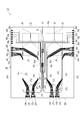
- Fig. 1 is a perspective view showing an optical module according to the first embodiment of the present invention
- Fig. 2 is a plan view of the optical module shown in Fig. 1
- Fig. 3 is a cross sectional view of the optical module taken along the line III-III indicated in Fig. 2
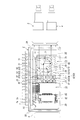
- Fig. 4 is a plan view of a semiconductor modulator installed within the optical module shown in Fig. 1
- Fig. 5 is a plan view of the semiconductor modulator shown in Fig. 4, where Fig. 5 removes interconnections and electrodes appearing in Fig. 4
- Fig. 6 is a flow chart of a process of assembling the optical module shown in Fig. 1
- Fig. 7 shows a step of a process of assembling the optical module
- Fig. 1 is a perspective view showing an optical module according to the first embodiment of the present invention
- Fig. 2 is a plan view of the optical module shown in Fig. 1
- Fig. 3 is a cross sectional view of the optical module taken along the
- Fig. 8 shows a step of the process subsequent to the step shown in Fig. 7;
- Fig. 9 shows a step of the process subsequent to the step shown in Fig. 8;
- Fig. 10 shows a step of the process subsequent to the step shown in Fig. 9;
- Fig. 11 shows a step of the process subsequent to the step shown in Fig. 10;
- Fig. 12 shows a step of the process subsequent to the step shown in Fig. 11;
- Fig. 13 is a perspective view of another optical module according to the second embodiment of the invention;
- Fig. 14 schematically shows positional relations between the arrayed lens and the input port and the first and second output ports in the semiconductor modulator during the alignment of the lens array.
- Fig. 1 is a perspective view of an inside of an optical module 1 according to the present invention
- Fig. 2 is a plan view of the optical module 1
- Fig. 3 is a cross sectional view of the optical module 1 taken along the line III-III appearing in Fig. 2, where Fig. 1 partially cuts one of side walls 2D, an input assembly 3, and an output assembly 4.
- the optical module 1 of the present embodiment which may be implemented in an optical communication system using the DP-QPSK configuration, provides a box-shaped housing 2, a side wall 2A in one of lateral sides of the housing 2, and the input assembly 3 and the output assembly 4 attached to the side wall 2A.
- the housing 2 which is made of, for instance Kovar TM , provides for side walls, 2A to 2D, and a bottom 2E.
- Two side walls, 2A and 2B face to each other extending in the lateral direction of the housing 2, while, other two side walls, 2C and 2D, also face to each other but extending in the longitudinal direction of the housing 2.
- the bottom 2E builds the four side walls, 2A to 2D, in a periphery thereof.
- the side wall 2A provides two windows 5, to which the input assembly 3 and the output assembly 4 are aligned, while, the side wall 2B facing the former side wall 2A provides a feedthrough 6 that implements transmission lines for carrying high frequency signals.
- the transmission lines receive the high frequency signals through a flexible printed circuit (FPC) board fixed thereto and transmit those high frequency signals within the housing 2.
- the FPC may be replaced to lead terminals.
- the side wall 2C also provides another feedthrough 7, refer to Fig. 2, where the feedthrough 7 has lead terminals 7a; specifically, the lead terminals 7a are fixed to both of a top surface and a back surface of the feedthrough 7, which may increases the count of the lead terminals.
- the optical module 1 of the present embodiment shows a complicated function requesting a number of control signals and biases; a great number of the lead terminals 7a arranged in both surfaces of the feedthrough 7 become inevitable.
- the lead terminals 7a which are connected with an external circuit board that mounts the optical module 1 thereon, include those for externally extracting signals generated and formed within the optical module 1, those for supplying biases to components installed within the housing 2, those for providing a ground potential, and so on.
- the embodiment of the optical module 1 provides the feedthrough 7 only in the side wall 2C, but, in an alternative, the housing 2 may provide still another feedthrough in the side wall 2D.
- the input assembly 3 and the output assembly 4 are disposed side by side along the lateral direction of the housing 2.
- the input assembly 3, as shown in Fig. 1, receives a polarization maintaining fiber (PMF) 8, and includes a coupling part for securing the PMF 8, what is called, a pig-tailed arrangement, and a lens 3a facing the window 5.
- the lens 3a which converts a continuous beam L 1 into a collimated beam to be provided within the housing 2, has a focal length of, for instance, 2.0 mm.
- the coupling part and the lens 3a are fixed to each other through a metal member.
- the output assembly 4, which receives a single mode fiber (SMF) 9, includes a coupling part for securing the SMF 9 and a lens 4a facing the window 5, where the lens 4a concentrates a output beam L 4 modulated in the DP-QPSK algorithm in the housing 2 onto the SMF 9.
- the lens 4a may have a focal length of, for instance, 2.0 mm.
- the coupling part and the lens 4a are fixed to each other through a metal member.
- the housing 2 also provides a lid, which is not illustrated in figures, on the sides walls, 2A to 2D, to enclose a space air-tightly. A space demarcated by the bottom 2E, the side walls, 2A to 2D, and the lid may enclose optical and electrical components air-tightly therein.
- the optical module 1 of the embodiment further provides a thermo-electric cooler (TEC) 10, a base 11, a carrier 12, and a semiconductor modulator 13 within the space.
- TEC 10 is mounted on the bottom 2E
- the base 11 is mounted on the TEC 10
- the semiconductor modulator 13 is mounted on the base 11, where the semiconductor modulator 13 in a temperature thereof is kept constant by the TEC 10.
- Fig. 4 is a plan view showing the semiconductor modulator 13, and Fig. 5 is also a plan view of the semiconductor modulator 13 but removes electronic elements such as interconnections and electrodes from those shown in Fig. 4.
- the semiconductor modulator 13 may be made of gallium arsenide (GaAs) and/or semiconductor materials grouped in GaAs.
- the semiconductor modulator 13 includes a modulator element 2o, an input port 21, first and second output ports, 22 and 23, a splitter 24, first and second combiners, 25 and 26, some arm waveguides, 27a to 27h, and first and second monitor ports, 28 and 29.
- the modulator element 20 which has a substrate made of insulating or semi-insulating InP, has a rectangular or a square plane shape with two longitudinal sides, 20a and 20b, and two lateral sides, 20c and 20d, where the former sides, 20a and 20b, preferably provide a length of 4 to 9 mm, while, the latter sides, 20c and 20d, preferably provide a length of 3 to 12 mm.
- the input port 21, which receives a continuous beam L 1 from the input assembly 3, is provided in one of the longitudinal sides 20a; specifically, in a center of the longitudinal side 20a. That is, the input port 21 has a distance to one of the lateral sides 20c that is substantially equal to a distance to another of the lateral sides 20d.
- the input port 21 has an optical axis perpendicular to the longitudinal side 20a; that is, an optical waveguide extending from the input port 21 has the optical axis that is perpendicular to the longitudinal side 20a.
- the first and second output ports, 22 and 23, which output output beams, L 2 and L 3 , externally, are provided also in the longitudinal side 20a in positions symmetrical with respect to the input port 21. That is, the first output port 22, which is set in a side closer to one of the lateral sides 20d, sets a distance to the input port 21 that is substantially equal to a distance for the second output port 23, which is set in another side closer to the other of the lateral side 20c, against the input port 21.
- the first and second output ports, 22 and 23, have optical axes perpendicular to the longitudinal side 20a; that is, optical waveguides extending from the first and second output ports, 22 and 23, have respective optical axes perpendicular to the longitudinal side 20a.
- a distance between the optical axes of the input port 21 and the first output port 22 is equal to a distance between the optical axes of the input port 21 and the second output port 23. Also, the first output port 22 has a distance against the lateral side 20d that is equal to a distance from the second output port to the other lateral side 20c.
- the splitter 24 splits the continuous beam L 1 entering in the input port 21 into eight beams each propagating in the arm waveguides, 27a to 27h.
- the first combiner 25 combines a part of the beams propagating in the four arm waveguides, 27e to 27h, and provides thus combined beams in the first output port 22 as the first output beam L 2 .
- the second combiner 26 combines rest of signal beams propagating in the other four arm waveguides, 27a to 27d, and provides thus combined beams in the second output port 23 as the second output beam L 3 .
- the first monitor port 28 monitors magnitude of a beam output from the first combiner 25, while, the second monitor port 29 monitors magnitude of a beam output from the second combiner 26.
- Those two monitor ports, 28 and 29, are disposed in the longitudinal side 20a, exactly, in respective positions at the longitudinal side 20a symmetrical with respect to the input port 21.
- the first and second output ports, 22 and 23, and the input port 21 are disposed inside of the first and second monitor ports, 28 and 29.
- the first monitor port 28 is disposed between the first output port 22 and one of the lateral side 20d, while, the second monitor port 29 is disposed between the second output port 23 and the other of the lateral side 20c.
- a distance from the first monitor port 28 to the input port 21 is substantially equal to a distance from the second monitor port 29 to the input port 21. Because the input port 21 is provided in the center of the longitudinal side 20a, a distance from the first monitor port 28 to the lateral side 20d is substantially equal to a distance from the second monitor port 29 to the other lateral side 20c.
- the semiconductor modulator 13 provides eight modulating electrodes, 31a to 31h, four primary phase-adjusting electrodes, 32a to 32d, and eight secondary phase-adjusting electrodes, where the secondary phase-adjusting electrodes are not illustrated in Fig. 4.
- the modulating electrodes, 31a to 31h overlap with the arm waveguides, 27a to 27h, to electrically modulate the beams propagating in the arm waveguides, 27a to 27h, by modifying refractive indices of material constituting the arm waveguides, 27a to 27h, which resultantly modifies the phases of the beams propagating within the arm waveguides, 27a to 27h.
- One of ends of the modulating electrodes, 31a to 31h, are connected with signal pads, 33a to 33h, through respective interconnections, where the signal pads, 33a to 33h, are coupled with the transmission lines on the feedthrough 6 interposing the driver 42, refer to Fig. 1 to Fig. 3. While, another of the ends of the modulating electrodes, 31a to 31h, are connected with other signal pads, 34a to 34h, for terminating the modulating electrodes, 31a to 31h, and the interconnections.
- the primary phase-adjusting electrodes, 32a to 32d which overlap with the optical waveguides in the modulator element 20 to cause a direct current (DC) filed in the respective optical waveguides independently, which modifies refractive indices of the optical waveguides.
- the primary phase-adjusting electrodes, 32a to 32d are electrically connected with the bias pads, 35a to 35d, through respective interconnections.
- the secondary phase-adjusting electrodes are connected with the bias pads, 36a to 36h, for inputting control signals.
- the semiconductor modulator 13 shown in Fig. 4 and Fig. 5 disposes the signal pads, 34a to 34h, and the bias pads, 35a to 35d, and 36a to 36h, in the lateral sides, 20c and 20d, respectively. However, the semiconductor modulator 13 may dispose those pads, 34a to 34h, 35a to 35d, and 36a to 36h, in one of the lateral sides, 20c or 20d.
- the bias pads, 35a to 35d, and 36a to 36h, are electrically connected with lead terminals 7a provided in the feedthrough 7.
- the optical module 1 further provides a heat sink 40, a circuit board 41, and the driver 42 in the housing 2.
- the heat sink 40 is disposed on the bottom between the feedthrough 6 and the TEC 10 along the longitudinal direction of the housing 2.
- the heat sink 40 which is made of material having good thermal conductivity, for instance, aluminum nitride (AlN), mounts the circuit board 41 thereon.
- the circuit board 41 which is a type of multi-layered printed board, is electrically connected with the lead terminals 7a in the feedthrough 7.
- the driver 42 which is mounted on the circuit board 41, is electrically connected with the circuit board 41, exactly, interconnections provided on the circuit board 41, through bonding wires.
- the driver 42 is connected with the transmission lines on the feedthrough 6 and the semiconductor modulator 13 through bonding wires.
- the driver 42 amplifies and re-shapes the driving signals provided from the transmission lines on the feedthrough 6 and provided to the semiconductor modulator 13.
- the optical module 1, as shown in Fig. 1 to Fig. 3, further provides optical elements of a polarizer 50, mirrors, 51 and 52, and an input lens system 53 in order to optically couple the input assembly 3 with the input port 21 of the semiconductor modulator 13.
- Those optical elements, 50 to 53, are mounted on the base 11 through an adhesive.
- the polarizer 50 which is disposed on the optical axis of the input assembly 3, re-shapes the polarization of the continuous beam L 1 coming from the input assembly 3.
- the polarizer 50 may extract the polarization component of one of 0° or 90° as the continuous beam L 1 .
- the mirror 51 which is optically coupled with the input assembly 3 through the polarizer 50, reflects the continuous beam L 1 coming from the polarizer 50 toward the other mirror 52.
- the continuous beam L 1 outgoing from the mirror 51 and that incoming to the mirror 51 makes substantially a right angle.
- the mirror 52 which provides a reflecting surface that optically couples with the input port 21 and the mirror 51, is disposed closer to the side wall 2D compared with the mirror 51 and on an optical axis of the input port 21.
- the mirror 52 which receives the continuous beam L 1 from the mirror 51, reflects the continuous beam L 1 toward the input port 21.
- the optical axis of the continuous beam L 1 in the incoming part and the outgoing part thereof makes a right angle, which means that the optical axis of the continuous beam L 1 in the outgoing part thereof becomes parallel to the optical axis of the input assembly 3; that is, the set of the mirrors, 51 and 52, makes the parallel translation of the optical axis of the input assembly 3 so as to align with the optical axis of the input port 21.
- the input lens system 53 is disposed on the optical axis of the input port 21 between the mirror 52 and the input port 21 and faces the input port 21.
- the input lens system 53 which concentrates the continuous beam L 1 reflected by the mirror 52 onto the input port 21, includes a rear lens 54 and a front lens 55, where the rear lens 54 is disposed closer to and faces the input port 21, while, the front lens 55 interposes the rear lens 54 with respect to the input port 21.
- the rear lens 54 may have a focal length of, for instance, 0.51 mm.
- the front lens 55 which is disposed between the rear lens 54 and the mirror 52, may have a focal length of, for instance, 2.1 mm.
- the continuous beam L 1 passes three lenses in an optical path from the PMF 8 to the input port 21, namely, that provided in the input assembly 3, the front lens 55, and the rear lens 54.
- the continuous beam L 1 is output from the PMF 8, converted into a collimated beam by the lens 3a in the input assembly 3, and concentrated onto the input port 21 by a combination of the front lens 55 and the rear lens 54.
- the front lens 55 is not always necessary; that is, the continuous beam L 1 is concentrated onto the input port 21 only by the rear lens 54 after converted into the collimated beam by the lens 3a.
- the optical module 1 further provides another optical coupling system for the first and second output lens systems, 60 and 63, where the optical coupling system includes a half-wavelength plate ( ⁇ /2) plate 66, where ⁇ is a wavelength of the continuous beam L 1 , a mirror 67, a skew adjustor 68, a polarization beam combiner (PBC) 69, and a beam splitter 70, each optically coupled with the output assembly 4, and two output ports, 22 and 23, in the semiconductor modulator 13.
- ⁇ /2 plate 66 where ⁇ is a wavelength of the continuous beam L 1
- a mirror 67 a mirror 67
- a skew adjustor 68 a skew adjustor 68
- PBC polarization beam combiner
- Those optical components are fixed on the base 11 with an adhesive after optically aligned with the semiconductor modulator 13.
- the first and second output lens systems, 60 and 63 are disposed in respective sides of the input lens system 53; specifically, the first output lens system 60 is arranged between the side wall 2C and the input lens system 53 so as to face the first output port 22, exactly, placed on the optical axis of the first output port 22.
- the first output lens system 60 which includes a rear lens 61 disposed relatively closer to the semiconductor modulator 13 and a front lens 62 disposed relatively apart from the semiconductor modulator 13, converts the output beam L 2 output from the first output port 22 into a collimated beam.
- the rear lens 61 which faces the first output port 22, has a focal length of, for instance, 0.51 mm; while, the front lens 62, which optically couples with the first output port 22 through the rear lens 61, is put between the rear lens 61 and the half-wavelength plate 66 and may have a focal length of, for instance, 2.1 mm.
- the second output lens system 63 which is disposed between the side wall 2D and the input lens system 53, faces the second output port 23, exactly, the second output lens system 63 is placed on the optical axis of the second output port 23 to convert the second output beam L 3 output from the second output port 23 of the semiconductor modulator 13 into a collimated beam.
- the second output lens system 63 also includes a rear lens 64 disposed relatively closer to the semiconductor modulator 13 and a front lens 65 disposes relatively apart from the semiconductor modulator 13.
- the rear lens 63 which is disposed so as to face the second output 23, may have a focal length of 0.51 mm.
- the front lens 65 which is also optically coupled with the second output port 23 but through the rear lens 64, is disposed between the skew adjustor 68 and the second output port 23.
- the front lens 65 may have a focal length of, for instance, 2.1 mm.
- the first output beam L 2 output from the first output port 22 passes three lenses, namely, the rear lens 61, the front lens 52 and the lens 42a in the output assembly 4. Specifically, the first output beam L 2 output from the first output port 22 as a divergent beam is converted into a collimated beam by a combination of the rear lens 61 and the front lens 62, multiplexed with the second output beam L 3 that is also a collimated beam, and finally concentrated onto the SMF 9 by the lens 4a in the output assembly 4.
- the front lens 62 is not unavoidable, that is, may be omitted. That is, the first output beam L 2 output from first output port 22 may be concentrated onto the SMF 9 through the rear lens 61 and the lens 4a.
- the other output beam L 3 output from the second output port 23 passes three lenses, namely, the rear lens 64, the front lens 65, and the lens 4a in the output assembly 4.
- the second output beam L 3 output from the second output port 23 as a divergent beam is converted into a collimated beam by a combination of the rear lens 64 and the front lens 65 in the second output lens system 63 and concentrated onto the SMF 9 by the lens 4a in the output assembly 4.
- the front lens 65 is not unavoidable, that is, may be removed from the optical coupling system.
- the second modulate beam L 3 may be concentrated onto the SMF 9 by the two lens system including the rear lens 64 and the lens 4a in the output assembly.
- the half-wavelength plate 66 which may be denoted as a ⁇ /2 plate and disposed on the optical axis of the front lens 62, rotates the polarization of the second output beam L 3 output from the second output port 23 by 90° so as to be orthogonal with the polarization of the first modulate beam L 2 output from the first output port 22.
- the embodiment shown in Fig. 2 disposes the ⁇ /2 plate 66 on the optical axis of the front lens 62, but the ⁇ /2 plate 66 may be provided on the optical axis of the other front lens 65 in the second output lens system 63.
- the ⁇ /2 plate 66 is necessary to be disposed on an optical axis of at least one of the front lenses, 62 and 65, to rotate the polarization of one of the output beams, L 2 or L 3 , so as to be orthogonal with the polarization of the other of the output beams, L 2 or L 3 .
- the mirror 67 which optically couples with the front lens 62 in the first output lens system 60 through the ⁇ /2 plate 66, reflects the first output beam L 2 passing the ⁇ /2 plate 66 toward the polarization beam combiner (PBC) 69.
- the first output beam L 2 in the optical axis of the incoming beam to the mirror 67 makes a right angle against the first output beam L 2 in the optical axis of the outgoing beam from the mirror 67.
- the skew adjuster 68 which may be a rectangular block made of silicon (Si), lengthens an equivalent optical length for the second output beam L 3 passing therethrough to compensate a phase delay caused in the first output beam L 2 by passing the ⁇ /2 plate 66. That is, the equivalent optical length of the skew adjuster 68 is substantially equal to an equivalent optical length of the ⁇ /2 plate 66.
- the second output beam L 3 reaches the PBC 69 passing the skew adjustor 68.
- the PBC 69 which optically couples with both of the first and second output ports, 22 and 23, is disposed on the optical axis of the front lens 65 of the second output lens system 63, that is, on the optical axis of the second output port 23.
- the PBC 69 provides a polarization selective filter in one surface thereof facing the mirror 67, while, an anti-reflection film in another surface opposite to the former one.
- the polarization selective filter shows substantial reflectance, namely substantially no transmittance, for a beam with a polarization parallel to an incident plane, while shows substantial transmittance, or substantially no reflectively, for a beam with a polarization perpendicular to the incident plane, where the incident plane is formed by an optical axis of a beam incoming there to and a normal of the filter.
- the polarization selective filter shows substantial transmittance, namely substantially no reflectance, for a beam with a polarization parallel to the incident plane, while shows substantial reflectance, namely substantially no transmittance, for a beam with a polarization perpendicular to the incident plane.
- the first output beam L 2 which is output from the first output port 22, is reflected toward the PBC 69 by the mirror 67 and reflected again by the PBC 69 toward the output assembly 4.
- the second output beam L 3 passing the skew adjuster 68, enters the PBC 69. Because two output beams, L 2 and L 3 , have the polarization same to each other at the first and second output ports, 22 and 23, of the semiconductor modulator 13, but the former output beam L 2 enters the mirror 67 after passing the ⁇ /2 plate 66 that rotates the polarization thereof by 90°; accordingly, two output beams, L 2 and L 3 , has the polarization orthogonal to each other at the PBC 69.
- the PBC 69 may have substantial reflectance for the first output beam L 2 coming from the mirror 67 and to be reflected toward the output assembly 4; while, shows substantial transmittance for the second output beam L 3 coming from the skew adjuster 68 and to be transmitted toward the output assembly 4.
- the PBC 69 may multiplex two output beams, L 2 and L 3 .
- the BS 70 which is disposed between the PBC 69 and the output assembly 4, has a parallelepiped shape with an incoming surface and an outgoing surface parallel to each other, where the incoming surface provides a reflective film that reflects a portion of an incident beam, specifically reflectivity around 5 %, of the incident beam L 4 and transmits a rest (around 95 %) thereof, where the beam L 4 is generated by multiplexing the two output beams, L 2 and L 3 , at the PBC 69.
- a beam reflected by the BS 70 enters a monitor photodiode (PD) 71 that is electrically connected with one of lead terminals 7a.
- the monitor PD 71 may generate an electrical signal corresponding to power of a beam split by the BS 70 from the multiplexed beam L 4 . Rest of the multiplexed beam L 4 enters the output assembly 4.
- the optical module 1 further provides other monitor PDs, namely, first and second monitor PDs, 80 and 81, in the housing 2, specifically in respective sides of the rear lenses, 61 and 64, in the output lens systems, 60 and 63, and on the base 11.
- the first and second monitor PDs, 80 and 81 are disposed sandwiching the rear lenses, 54, 61, and 64.
- the first monitor PD 80 which is disposed on the optical axis of the first monitor port 28 between the rear lens 61 and the side wall 2C, faces the first monitor port 28 of the semiconductor modulator 13.
- the first monitor PD 80 detects a monitor beam output from the first monitor port 28 and generates a signal corresponding to power of the monitor beam.
- the signal is output from one of the lead terminals 7a connected with the first monitor PD 80 with a bonding wire.
- the second monitor PD 81 which is disposed on the optical axis of the second monitor port 29 between the rear lens 64 of the second output lens system 63 and the sides wall 2D, faces the second monitor port 29.
- the second monitor PD 81 detects a monitor beam output from the second monitor port 29 and generates a signal corresponding to power of the detected monitor beam.
- the signal generated by the second monitor PD 81 is output through one of the lead terminals 7a connected with the second monitor PD 81 through a bonding wire.
- the optical module 1 further provides an anti-reflection plate 85 one the base 11.
- the anti-reflection plate 85 is disposed behind the mirror 52, the PBC 69, and the BS 70; that is between components of the mirror 52, the PBC 69, and the BS 70, and the sides wall 2D.
- the continuous beam L 1 provided from the input assembly 3 is reflected toward the mirror 52 by the mirror 51.
- the continuous beam L 1 reaching the mirror 52 is almost reflected by the mirror 52; but a faint portion thereof transmits the mirror 52 to reach the anti-reflection plate 85.
- a faint portion of the first output beam L 2 reflected by the mirror 67 toward the PBC 69 transmits the PBC 69 and reaches the anti-reflection plate 85.
- the anti-reflection plate 85 may prevent those beams reaching thereto from the mirror 52 and the PBC 69 from being reflected by the side wall 2D.
- the optical module 1 thus described modulates the continuous beam L 1 entering through the input assembly 3 by the semiconductor modulator 13 after split into the arm waveguides, 27a to 27h.
- the optical circuit provided in downstream of the semiconductor modulator 13 rotates the polarization of one of the output beams L 2 by 90° and multiplexes the one of the output beams L 2 with the other of the output beam L 3 by the PBC 69.
- the PBC 69 outputs the multiplexed beam L 4 toward the output assembly 4.
- the optical module 1 may concurrently transmits information corresponding to four (4) bits.
- Fig. 6 is a flow chart of the process of assembling the optical module 1
- Fig. 7 to Fig .12 are plan views of the optical module 1 at respective steps of the process.
- the process installs optical components including the semiconductor modulator 13 within the housing 2 at a step P 1 .
- the rear lens 54 of the input lens system 53 will be optically aligned at steps P 2 .
- the process prepares a dummy fiber 90 that emulates the input assembly 3, where Fig. 7 to Fig. 11 schematically illustrates the dummy fiber 90.
- the dummy fiber 90 may output a test beam TL 1 used in optical alignment of the input lens system 53.
- the test beam TL 1 provided from the dummy fiber 90 which is a continuous wave (CW) and has a wavelength equal to a wavelength of the continuous beam L 1 , is a collimated beam converted by a lens that is not illustrated in the figures.
- CW continuous wave
- the process first aligns the dummy fiber 90. As shown in Fig. 7, entering the test beam TL 1 within the housing 2 from the dummy fiber 90, the process detects magnitude of the test beam TL 1 reaching the input port 21 passing the polarizer 50 and the mirrors, 51 and 52 by at least one of the monitor PDs, 80 and 81. Sliding the dummy fiber 90 on the outer surface of the side wall 2A of the housing 2, the process determines the position of the dummy fiber 90 where the magnitude detected by one of the monitor PDs, 80 and 81, becomes a maximum. Because the test beam TL 1 is a collimated beam, the process may detect a maximum of the detected magnitude in spite of limited dimensions of the input port 21.
- the test beam TL 1 is preferably detected in maximum magnitude thereof by both of the first and second monitor PDs, 80 and 81, because the optical coupling efficiency becomes extremely small when the test beam TL 1 is directly coupled with the input port 21 without interposing any lenses.
- both of the first and second monitor PDs, 80 and 81 are utilized for detecting the magnitude of the test beam TL 1 , a sum of the outputs from the first and second monitor PDs, 80 and 81, becomes substantial and the evaluation of the magnitude becomes simple and easy.
- the process mounts the rear lens 54 onto the base 11 and disposes so as to face the input port 21.
- the test beam TL 1 may be utilized for aligning the rear lens 54.
- the test beam TL 1 entering the input port 21 passing the rear lens 54 is detected by the first and second monitor PDs, 80 and 81, slightly shifting a position of the rear lens 54 on the optical axis thereof to find a position where the magnitude of the test beam TL 1 detected by the first and second monitor PDs, 80 and 81, become maximum.
- the rear lens 54 is slightly shifted toward the semiconductor modulator 13 and fixed thereat to the base 11 by, for instance, ultraviolet curable resin.
- the process optically aligns the front lens 55 and fixes to the base 11 at step P 3 .
- the test beam TL 1 is provided from the dummy fiber 90 to enter the input port 21 through the front lens 55 and the rear lens 54.
- the first and second monitor PDs, 80 and 81 detect the magnitude of the test beam TL 1 as slightly shifting the position of the front lens 55 along the optical axis thereof to find a position where the test beam TL 1 detected by the first and second monitor PDs, 80 and 81, becomes maximum.
- the front lens 55 is fixed to the base 11 with ultraviolet curable adhesive.
- the process aligns the first and second output lens systems, 60 and 63.
- the process adjusts the semiconductor modulator 13. Specifically, the semiconductor modulator 13 in phase statuses in respective waveguides are adjusted such that the test beams, TL 2 and TL 3 , each output from the first and second output ports, 22 and 23, become maxima by varying biases supplied to the semiconductor modulator 13.
- the biases that maximize intensities of the output beams, L 2 and L 3 are determined in advance to the adjustment at step P 6 described later.
- the process mounts the rear lenses, 61 and 64, onto the base 11 such that the rear lens 61 faces the first output port 22, while, the rear lens 64 faces the second output port 23.
- a camera 91 is prepared outside of the optical module 1.
- the camera 91 is placed so as to face the side wall 2A to which the output assembly 4 is to be attached such that the camera 91 becomes enough apart from the side wall 2A.
- entering the test beam TL 1 into the input port 21 from the dummy fiber 90, the first output port 22 outputs the test beam TL 2 and the second output port 23 outputs the test beam TL 3 refer to Fig. 10 to Fig. 12.
- biases are supplied such that only the second output port 23 outputs the test beams TL 3 , that is, substantially no test beam TL 2 is output from the first output port 22. Inspecting a field pattern of the test beam TL 3 coming from the second output port 23 by the camera 91, the rear lens 64 is aligned such that the inspected profile of the test beam TL 3 becomes that of a collimated beam. Also, when the rear lens 61 in the first output lens system 60 is to be aligned, biases are supplied to the semiconductor modulator 13 such that only the first output port 22 outputs the test beam TL 2 .
- the rear lens 61 Inspecting the field pattern of the test beam TL 2 by the camera 91, the rear lens 61 is aligned such that the inspected pattern of the test beam TL 2 becomes that of the collimated beam. Finally, the rear lenses, 61 and 64, are slightly shifted along the optical axes thereof so as to be apart from the semiconductor modulator 13 from points where the maximum intensity of the test beams, TL 2 and TL 3 , are observed. After slightly shifting the rear lenses, 61 and 64, the rear lenses, 61 and 64, are fixed to the base 11 with adhesive curable by ultraviolet rays.
- the front lenses, 62 and 65, in the first and second output lens systems, 60 and 63, respectively, are installed within the housing 2 at step P 5 .
- the front lenses, 62 and 65 are placed on the base 11 so as to face the first and second output ports, 22 and 23, through the respective rear lenses, 61 and 64, to align with the semiconductor modulator 13 and fix to the base 11.
- the process sets the front lenses, 62 and 65, in respective positions where the test beams, TL 2 and TL 3 , become collimated beams.
- the process prepares another dummy fiber 92, where Fig. 11 schematically illustrates the dummy fiber 92.
- the dummy fiber 92 which emulates the output assembly 4 and provides a lens that concentrates a test beam entering therein onto the dummy fiber 92.
- the process aligns the dummy fiber 92 so as to optically couple with the front lenses, 62 and 65.
- the semiconductor modulator 13 entering the test beam TL 1 in the semiconductor modulator 13 from the dummy fiber 90, the semiconductor modulator 13 outputs the test beams, TL 2 and TL 3 , from the first and second output ports, 22 and 23.
- the process may selects one of the output ports, 22 or 23, to output the test beam, TL 2 or TL 3 , by adjusting biases supplied to the semiconductor modulator 13.
- the process next compares maximum power of the test beam TL 2 with maximum power of the other test beam TL 3 at step P 6 , where the maximum power of the test beams, TL 2 or TL 3 , is the power detected through the dummy fiber 92.
- the process first adjusts the bias provided to the semiconductor modulator such that only one of the output ports, 22 and 23, generates the test beam, TL 2 or TL 3 .
- this test beam TL 2 enters the dummy fiber 92 passing the rear lens 61 and the front lens 62.
- the front lens 62 may be adjusted in a position where the test beam TL 2 detected through the dummy fiber 92 shows maximum power.
- the test beam TL 3 enters the dummy fiber 92 passing the rear lens 64 and the front lens 65. Accordingly, the front lens 65 is set in a position where the test beam TL 3 detected through the dummy fiber 92 shows maximum power.
- Step P 6 sets the biases supplied to the semiconductor modulator 13 such that the test beams, TL 2 and TL 3 , show respective maximum power, where bias conditions at which the test beams, TL 2 and TL 3 , show the respective maximum power may be determined such that bias conditions that shows the power of the first test beam TL 2 becomes maximum are first determined, then another bias conditions that shows the power of the second test beam TL 3 becomes maximum.
- the process also finds bias conditions that minimizes the power of the first test beam TL 2 and another bias conditions that also minimizes the power of the second test beams TL 3 .
- the maximum power of the test beam TL 2 inevitably becomes different from the maximum power of the other test beam TL 3 because optical losses attributed to the waveguides in the semiconductor modulator 13 are difference from each other, and those of the optical coupling systems from the first output port 22 to the dummy fiber 92 and from the second output port 23 to the dummy fiber 92, such as the mirror 67 and/or the PBC 69, are also difference from each other.
- the embodiment of the present process first fixes one of the front lenses, 62 or 65, that shows greater maximum power for the dummy fiber 92 at a step P 7 . Then, another front lens, 62 or 65, that shows smaller maximum power for the dummy fiber 92 is subsequently fixed.
- the front lens, 62 or 65, showing the greater maximum power is aligned along the optical axis thereof such that the power of the test beam, TL 2 or TL 3 , detected through the dummy fiber 92 becomes closer to the smaller maximum power, or becomes substantially equal to the smaller maximum power, obtained for the other of the front lens, 62 or 65, at a step P 8 .
- An adhesive such as ultraviolet curable resin, may permanently fix the front lenses, 62 and 65, on the base 11 after the alignment thereof at a step P 9 .
- the process attaches the lid to the side walls, 2A to 2D, and replaces the dummy fibers, 90 and 92, with the input and output assemblies, 3 and 4, respectively.
- the input and output assemblies, 3 and 4 may be welded by YAG-laser to the housing 2. Specifically, entering the continuous beam L 1 from the input assembly 3, the output beams, L 2 and L 3 , are detected through the output assembly 4 as aligning the input and output assemblies, 3 and 4, against the housing 2, which is often called as a three-body alignment. Sliding the input and output assemblies, 3 and 4, on the side wall 2A, the positions of the assemblies, 3 and 4, are determined at which one of the output beams, L 2 or L 3 , becomes a maximum at a step P 10 .
- the positions of the assemblies, 3 and 4 become equal to the positions of the dummy fibers, 90 and 92.
- the biases supplied to the semiconductor modulator 13 are set such that one of the output beams, L 2 or L 3 , becomes a maximum.
- the YAG laser welding may fix the assemblies with the side wall 2A.
- the input assembly 3 is adjusted in a rotation angle thereof to be the designed angle.
- the semiconductor modulator 13 of the present embodiment provides the input port 21 and two output ports, 22 and 23, only in one side 20a of the modulator element 20, the optical components that couple those optical ports, 21 to 23, with the input assembly 3 and the output assembly 4 may be disposed only in one side of the modulator element 20 in the housing 2, which may make the optical module 1 compact.
- the arrangement of the two output ports, 22 and 23, disposed symmetrically with respect to the input port 21 may enhance design flexibility of the dispositions of those optical components.
- the arrangement of the first output port 22 enough apart from the second output port 23 may widen effective areas for placing the respective optical components and increase the flexibility of the dispositions thereof.
- the semiconductor modulator 13 with the input and output ports, 21 to 23, only in one of sides 20a makes the optical alignment of the components effective and simple, which also makes the production of the optical module 1 simple.
- This arrangement where the semiconductor modulator 13 sets an area facing the side 20a for mounting the optical components, an area facing the side 20d for wiring to the lead terminals 7a, and an area facing the side 20b for mounting the driver 42, may use the respective areas effectively and make the production of the optical module 1A simple.
- the first output beam L 2 output from the first output port 22 passes three lenses, 61, 62, and 4a, to the SMF 9; while the second output beam L 3 output from the second output port 23 also passes three lenses, 64, 65, and 4a, to the SMF 9.
- the process first aligns the rear lenses, 61 and 64, that are necessary to be precisely disposed because of the substantial magnification ratio thereof, then aligns the front lenses, 62 and 65, which sets the SMF 9 effectively aligned with the first and second output ports, 22 and 23.
- the rear lens, 61 or 64 In the two-lens system having a rear lens, 61 or 64, and a front lens 3a, that is the lens 3a in the input assembly operates as the front lens in the embodiment and the front lens, 62 or 65, is omitted, the rear lens, 61 or 64, is inevitably requested to be precisely aligned, typically less than 0.3 ⁇ m, to suppress optical losses due to positional deviations of the lens.
- those lenses, 61 and 64 are fixed with a resin, typically, with an ultraviolet curable resin, and the resin usually shrinks during solidifying or expands by heat treatment, which makes hard for once aligned optical components to maintain positional preciseness, or to maintain positional preciseness smaller than 1.0 ⁇ m.
- the three lens system like the present embodiment may alleviate the positional preciseness in the front lens put between the lenses compared with the two lens system. Preciseness greater than 1.5 ⁇ m may be sometimes allowed.
- the center lens in the assembly thereof becomes simple and easy.
- the front lens, 62 or 65 may be disposed closer to the rear lens, 61 or 64, to convert the beam output from the front lens, 62 or 65, into a collimated beam, which may shorten the longitudinal dimension of the housing 2.
- the first and second monitor ports, 28 and 29, are symmetrically disposed with respect to the input port 21 in the side 20a; the first and second output ports, 22 and 23, and the input port 21 are disposed between the monitor ports, 28 and 29; and the first and second monitor PDs, 80 and 81, are disposed facing the first and second monitor ports, 28 and 29.
- This arrangement may dispose the first and second monitor PDs, 80 and 81, in respective sides of the first and second output lens systems, 60 and 63, which may make the housing 2 of the optical module 1 compact.
- the SMF 9 may be disposed on the axis of the output port 23, which may save an additional mirror that rearranges the optical axis of the second output beam L 3 output from the second output port 23 with respect to the axis of the SMF 9; resultantly, may decrease the number of components to be installed within the housing 2.
- the optical module 1 may provide the mirror 52 that reflects the continuous beam L 1 propagating along the lateral direction of the housing 2 toward the input port 21, the PBS 69 that reflects the first output beam L 2 also propagating along the lateral direction and multiplexes thus reflected first output beam L 2 with the second output beam L 3 , and the anti-reflection plate 85 that is disposed facing the mirror 52 and the PBS 69 along the longitudinal direction of the housing 2 and prevents the output beams, L 2 and L 3 , that transmit the mirror 52 and the PBS 69 from being reflected at the side wall 2D of the housing 2.
- the anti-reflection plate 85 may suppress stray beams caused within the housing 2, which suppresses degradation in the performances of the optical module 1.
- the optical module 1 may reduce the number of components installing therein and resultantly the cost thereof.
- the step P 2 first aligns the dummy fiber 90, then the rear lens 54 by the test beam TL 1 provided through the dummy fiber 90.
- the step P 5 optically couples the dummy fiber 92 with the output ports, 22 and 23, first; the front and rear lenses, 62 and 65, are secondly aligned with the output ports, 22 and 23, and finally aligns the dummy fiber 92 with the front and rear lenses, 65 and 62.
- This alignment procedure may make the process of assembling the optical module 1 simple and efficient.
- the process of assembling the optical module 1 may include steps of P 6 to P 8 in which one of the front lens, 62 or 65, that shows smaller maximum power for the test beam TL 2 with respect to the dummy fiber 92 is first fixed, then the other front lens, 62 or 65, is subsequently fixed.
- the step P 8 may align one of the front lenses, 62 or 65, that shows a greater coupling power along the optical axis thereof such that the coupling power with respect to the dummy fiber 92 becomes substantially equal to, or closer to the smaller maximum power for the dummy fiber 92; then, fixes the one of the front lenses, 62 and 65, thereat.
- the steps P 7 to P 8 may balance the power of the output beams, L 2 and L 3 , output from the respective output ports, 22 and 23; and in addition, the power of the output beams, L 2 and L 3 , may be set closer to the respective maxima.
- the step P 8 may adjust the semiconductor modulator 13 in phase statuses thereof such that the test beams, TL 2 and TL 3 , output from the output ports, 22 and 23, become respective maxima.
- the test beams, TL 2 and TL 3 are not always set to be respective maxima.
- Such a status sometimes sets the power of the output beams, L 2 and L 3 , output from the output ports, 22 and 23, unbalanced. Adjusting the phase status of the semiconductor modulator 13, the power of the output beams, L 2 and L 3 , may balance.
- FIG. 13 is a perspective view of an optical module 1A according to the second embodiment of the present invention.
- the optical module 1A has a feature distinguishable from the optical module 1 of the first embodiment that the three lens systems, 53, 60 and 63, that optically couples the input port 21 of the semiconductor modulator 13 with the input assembly 3 and the output ports, 22 and 23, with the output assembly 4 are replaced to an arrayed lens 60A that integrates three lens elements.
- Fig. 14 is a front view that illustrates a positional relation between the arrayed lens 60A and the semiconductor modulator 13, in particular, the side 20a thereof providing the input port 21 and the output ports, 22 and 23. Because six lenses in the two lens systems, 53, 60, and 63, are replaced to one arrayed lens 60A, the optical module 1A may further decrease the number of components installed within the housing 2.
- the arrayed lens 60A provides three lens elements each having optical axes with spans to neighbor lens element substantially equal to a span between the input port 21 and the output ports, 22 and 23. Also, because the arrayed lens 60A integrally provides three lens elements, once aligned status between one lens element and one port in the semiconductor modulator 13 is possibly miss-aligned during the optical alignment for the rest lens elements.
- the alignment process for the arrayed lens 60A accordingly, carries out the alignment for the lens elements disposed outer sides thereof but no alignment is done for the rest lens element disposed in the center.
- the lens element in the center is automatically positioned by aligning the lens elements provided in the outer sides. Specifically, entering a test beam into the output port 22 through one of the lens element provided in the outer sides and detecting thus entered test beam by electrodes inherently accompanied with the arm waveguides in the semiconductor modulator 13. Although the electrodes in the arm waveguides are provided for generating signal beams, L 2 and L 3 , each modulated by the modulation signals, the process of assembling the arrayed lens 60A uses those electrodes for detecting power of the test beam entering from the output ports, 22 and 23.
- the assembling process determines and memorizes the position of the arrayed lens 60A for the one of the output port 22. Thereafter, the alignment process carries out similar procedures for another lens element oppositely arranged with respect to a center of the arrayed lens 60A and the other output port 23. Then, the process determines and memorizes the position of the arrayed lens 60A. However, during the latter alignment, the position of the former lens element is possibly and inevitably deviated from the aligned position. Accordingly, the alignment process may calculate the position of the arrayed lens 60A from two sets of the positions each determined in the first and second aligning process and memorized in the system. The position of the center lens element may be automatically determined to the calculated position.
Landscapes
- Physics & Mathematics (AREA)
- General Physics & Mathematics (AREA)
- Optics & Photonics (AREA)
- Nonlinear Science (AREA)
- Engineering & Computer Science (AREA)
- Computer Networks & Wireless Communication (AREA)
- Signal Processing (AREA)
- Electromagnetism (AREA)
- Optical Modulation, Optical Deflection, Nonlinear Optics, Optical Demodulation, Optical Logic Elements (AREA)
- Optical Couplings Of Light Guides (AREA)
Abstract
L'invention concerne un module optique qui fournit un modulateur à semi-conducteur, un système de lentille d'entrée et des premier et second systèmes de lentilles de sortie, et deux photodiodes de surveillance. Le modulateur à semi-conducteur fournit un port d'entrée, des premier et second ports de sortie, et deux ports de surveillance dans un côté de celui-ci. Le port d'entrée et les premier et second ports de sortie font face au système de lentille d'entrée et aux premier et second systèmes de lentille, respectivement. Les deux ports de surveillance font face aux deux photodiodes de surveillance, respectivement. Les premier et second ports de sortie sont disposés symétriquement par rapport au port d'entrée d'un côté. Les deux ports de surveillance sont disposés dans des côtés extérieurs respectifs des premier et second ports de sortie et symétriquement par rapport au port d'entrée.
Priority Applications (3)
| Application Number | Priority Date | Filing Date | Title |
|---|---|---|---|
| US16/957,920 US11347126B2 (en) | 2017-12-26 | 2018-12-26 | Optical module and process of assembling the same |
| JP2020534625A JP2021509483A (ja) | 2017-12-26 | 2018-12-26 | 光モジュール及び光モジュールの組立方法 |
| CN201880083506.XA CN111512218B (zh) | 2017-12-26 | 2018-12-26 | 光学模块及其组装方法 |
Applications Claiming Priority (2)
| Application Number | Priority Date | Filing Date | Title |
|---|---|---|---|
| JP2017249023 | 2017-12-26 | ||
| JP2017-249023 | 2017-12-26 |
Publications (1)
| Publication Number | Publication Date |
|---|---|
| WO2019131804A1 true WO2019131804A1 (fr) | 2019-07-04 |
Family
ID=67067470
Family Applications (1)
| Application Number | Title | Priority Date | Filing Date |
|---|---|---|---|
| PCT/JP2018/047950 Ceased WO2019131804A1 (fr) | 2017-12-26 | 2018-12-26 | Module optique et procédé d'assemblage de celui-ci |
Country Status (4)
| Country | Link |
|---|---|
| US (1) | US11347126B2 (fr) |
| JP (1) | JP2021509483A (fr) |
| CN (1) | CN111512218B (fr) |
| WO (1) | WO2019131804A1 (fr) |
Cited By (4)
| Publication number | Priority date | Publication date | Assignee | Title |
|---|---|---|---|---|
| WO2021188466A1 (fr) * | 2020-03-16 | 2021-09-23 | Lightmatter, Inc. | Réalisation d'une forte puissance optique par mode avec des sources lumineuses intégrées et combineurs optiques |
| US11409045B2 (en) | 2019-07-02 | 2022-08-09 | Lightmatter, Inc. | Photonics stabilization circuitry |
| US12355492B2 (en) | 2023-09-27 | 2025-07-08 | Lightmatter, Inc. | Spectrally interleaved optical transceivers |
| US12498292B2 (en) | 2022-08-30 | 2025-12-16 | Sumitomo Electric Industries, Ltd. | Method of assembling optical module |
Families Citing this family (14)
| Publication number | Priority date | Publication date | Assignee | Title |
|---|---|---|---|---|
| US11606145B2 (en) * | 2021-01-29 | 2023-03-14 | Alpine Optoelectronics, Inc. | Silicon photonics based single-wavelength 100 gbit/S PAM4 DWDM transceiver in pluggable form factor |
| JP7381174B2 (ja) * | 2021-05-21 | 2023-11-15 | 三菱電機株式会社 | 光モジュール |
| JP7704027B2 (ja) * | 2021-12-22 | 2025-07-08 | 住友電気工業株式会社 | 光モジュール、及び光モジュールの製造方法 |
| JP7803192B2 (ja) | 2022-03-30 | 2026-01-21 | 住友大阪セメント株式会社 | 光デバイスとそれを用いた光送信装置 |
| CN115343811A (zh) * | 2022-04-21 | 2022-11-15 | 讯芸电子科技(中山)有限公司 | 蝶型封装光收发器 |
| JP2024033275A (ja) * | 2022-08-30 | 2024-03-13 | 住友電気工業株式会社 | 光モジュール |
| JPWO2024075171A1 (fr) * | 2022-10-03 | 2024-04-11 | ||
| WO2024075167A1 (fr) * | 2022-10-03 | 2024-04-11 | 日本電信電話株式会社 | Émetteur optique |
| WO2024075172A1 (fr) * | 2022-10-03 | 2024-04-11 | 日本電信電話株式会社 | Émetteur optique |
| US20260104602A1 (en) * | 2022-10-03 | 2026-04-16 | Ntt, Inc. | Optical Transmitter |
| US20260104606A1 (en) * | 2022-10-03 | 2026-04-16 | Nippon Telegraph And Telephone Corporation | Optical Transmitter |
| WO2024075170A1 (fr) * | 2022-10-03 | 2024-04-11 | 日本電信電話株式会社 | Émetteur optique |
| WO2024075169A1 (fr) * | 2022-10-03 | 2024-04-11 | 日本電信電話株式会社 | Émetteur optique |
| US20240302607A1 (en) * | 2023-03-10 | 2024-09-12 | Ii-Vi Delaware, Inc. | Optical electronic device and manufacturing method thereof |
Citations (5)
| Publication number | Priority date | Publication date | Assignee | Title |
|---|---|---|---|---|
| US20140308047A1 (en) * | 2013-04-11 | 2014-10-16 | Ciena Corporation | Optimum modulator bias systems and methods in coherent optical transmitters |
| US20170019181A1 (en) * | 2014-03-14 | 2017-01-19 | Oclaro Technology Limited | Optical Component |
| WO2017085447A1 (fr) * | 2015-11-20 | 2017-05-26 | Oclaro Technology Limited | Dispositif de modulation optique |
| US20170184802A1 (en) * | 2014-10-28 | 2017-06-29 | Sumitomo Electric Industries, Ltd. | Method of assembling the optical module implementing mach-zehnder modulator |
| US20170242316A1 (en) * | 2016-02-24 | 2017-08-24 | Mitsubishi Electric Corporation | Optical modulator element, optical modulation module including optical modulator element, and method for manufacturing optical modulator element |
Family Cites Families (32)
| Publication number | Priority date | Publication date | Assignee | Title |
|---|---|---|---|---|
| EP0773591A3 (fr) * | 1995-11-13 | 1998-09-16 | Sumitomo Electric Industries, Ltd. | Module émetteur/détecteur de lumière |
| US6043550A (en) * | 1997-09-03 | 2000-03-28 | Sumitomo Electric Industries, Ltd. | Photodiode and photodiode module |
| US6370290B1 (en) * | 1997-09-19 | 2002-04-09 | Uniphase Corporation | Integrated wavelength-select transmitter |
| US6766082B2 (en) * | 2000-10-18 | 2004-07-20 | Nippon Telegraph And Telephone Corporation | Waveguide-type optical device and manufacturing method therefor |
| WO2003005509A1 (fr) * | 2001-07-02 | 2003-01-16 | Furukawa Electric Co.,Ltd | Module laser a semiconducteur, amplificateur de lumiere et procede de production de module laser a semiconducteur |
| US7408867B2 (en) * | 2002-04-04 | 2008-08-05 | The Furukawa Electric Co., Ltd. | Method of aligning an optical fiber, method of manufacturing a semiconductor laser module, and semiconductor laser module |
| US6731841B1 (en) * | 2002-05-24 | 2004-05-04 | Alliance Fiber Optic Products, Inc. | Folded waveguide optical devices |
| US7275877B2 (en) * | 2003-04-30 | 2007-10-02 | Sumitomo Electric Industries, Ltd. | Optical module having individual housing for an optical processing unit and an optical sub-assembly |
| JP4658658B2 (ja) * | 2005-03-29 | 2011-03-23 | 住友大阪セメント株式会社 | 光変調器 |
| JP4183716B2 (ja) * | 2006-03-29 | 2008-11-19 | 住友大阪セメント株式会社 | 光導波路素子 |
| JP4842987B2 (ja) | 2008-03-19 | 2011-12-21 | 富士通株式会社 | 光デバイス |
| CN102472943A (zh) * | 2010-03-12 | 2012-05-23 | 松下电器产业株式会社 | 光学式声相关器 |
| US8923673B2 (en) * | 2011-02-23 | 2014-12-30 | Sumitomo Osaka Cement Co., Ltd. | Optical modulator |
| US20130051024A1 (en) * | 2011-08-31 | 2013-02-28 | Moshe Amit | Optical Transmitter Assembly, Optical Transceivers Including the Same, and Methods of Making and Using Such Optical Transmitter Assemblies and Optical Transceivers |
| TWI529438B (zh) * | 2012-04-26 | 2016-04-11 | 華星光通科技股份有限公司 | 光收發器模組 |
| JP2013246325A (ja) * | 2012-05-25 | 2013-12-09 | Sumitomo Osaka Cement Co Ltd | 光変調器 |
| TWI637197B (zh) * | 2013-08-09 | 2018-10-01 | 住友化學股份有限公司 | Optical film |
| TWI653149B (zh) * | 2013-08-09 | 2019-03-11 | 住友化學股份有限公司 | Optical film |
| JP6277660B2 (ja) * | 2013-10-16 | 2018-02-14 | 住友電気工業株式会社 | 全二重光トランシーバ |
| JP6446815B2 (ja) * | 2014-04-08 | 2019-01-09 | 住友電気工業株式会社 | 光接続構造 |
| JP6295811B2 (ja) * | 2014-05-08 | 2018-03-20 | 住友電気工業株式会社 | 光トランシーバ |
| JP6340902B2 (ja) * | 2014-05-13 | 2018-06-13 | 住友電気工業株式会社 | 光モジュールの製造方法 |
| US9780882B2 (en) * | 2014-05-13 | 2017-10-03 | Sumitomo Electric Industries, Ltd. | Optical transmitter module having multiple signal lanes |
| CN107078457A (zh) * | 2014-10-28 | 2017-08-18 | 住友电气工业株式会社 | 应用光源、光调制器和波长检测器的光学模块及其组装方法 |
| JP6435833B2 (ja) * | 2014-12-11 | 2018-12-12 | 住友電気工業株式会社 | 光モジュール |
| JP6375869B2 (ja) * | 2014-10-28 | 2018-08-22 | 住友電気工業株式会社 | 光モジュール |
| JP2016100468A (ja) * | 2014-11-21 | 2016-05-30 | 住友電気工業株式会社 | 光モジュール |
| JP6597427B2 (ja) * | 2016-03-16 | 2019-10-30 | 住友電気工業株式会社 | 光モジュールの製造方法 |
| JP6380069B2 (ja) * | 2014-12-11 | 2018-08-29 | 住友電気工業株式会社 | 光送信モジュール |
| US10246742B2 (en) * | 2015-05-20 | 2019-04-02 | Quantum-Si Incorporated | Pulsed laser and bioanalytic system |
| JP6661913B2 (ja) | 2015-07-28 | 2020-03-11 | 富士通オプティカルコンポーネンツ株式会社 | 光モジュール、及びこれを用いた光送信機 |
| JP6656140B2 (ja) * | 2016-02-24 | 2020-03-04 | 三菱電機株式会社 | 光変調器素子、それを備える光変調モジュールおよび光変調器素子の製造方法 |
-
2018
- 2018-12-26 JP JP2020534625A patent/JP2021509483A/ja active Pending
- 2018-12-26 WO PCT/JP2018/047950 patent/WO2019131804A1/fr not_active Ceased
- 2018-12-26 CN CN201880083506.XA patent/CN111512218B/zh active Active
- 2018-12-26 US US16/957,920 patent/US11347126B2/en active Active
Patent Citations (5)
| Publication number | Priority date | Publication date | Assignee | Title |
|---|---|---|---|---|
| US20140308047A1 (en) * | 2013-04-11 | 2014-10-16 | Ciena Corporation | Optimum modulator bias systems and methods in coherent optical transmitters |
| US20170019181A1 (en) * | 2014-03-14 | 2017-01-19 | Oclaro Technology Limited | Optical Component |
| US20170184802A1 (en) * | 2014-10-28 | 2017-06-29 | Sumitomo Electric Industries, Ltd. | Method of assembling the optical module implementing mach-zehnder modulator |
| WO2017085447A1 (fr) * | 2015-11-20 | 2017-05-26 | Oclaro Technology Limited | Dispositif de modulation optique |
| US20170242316A1 (en) * | 2016-02-24 | 2017-08-24 | Mitsubishi Electric Corporation | Optical modulator element, optical modulation module including optical modulator element, and method for manufacturing optical modulator element |
Cited By (6)
| Publication number | Priority date | Publication date | Assignee | Title |
|---|---|---|---|---|
| US11409045B2 (en) | 2019-07-02 | 2022-08-09 | Lightmatter, Inc. | Photonics stabilization circuitry |
| US11686902B2 (en) | 2019-07-02 | 2023-06-27 | Lightmatter, Inc. | Photonics stabilization circuitry |
| WO2021188466A1 (fr) * | 2020-03-16 | 2021-09-23 | Lightmatter, Inc. | Réalisation d'une forte puissance optique par mode avec des sources lumineuses intégrées et combineurs optiques |
| EP4121806A4 (fr) * | 2020-03-16 | 2024-04-10 | Lightmatter, Inc. | Réalisation d'une forte puissance optique par mode avec des sources lumineuses intégrées et combineurs optiques |
| US12498292B2 (en) | 2022-08-30 | 2025-12-16 | Sumitomo Electric Industries, Ltd. | Method of assembling optical module |
| US12355492B2 (en) | 2023-09-27 | 2025-07-08 | Lightmatter, Inc. | Spectrally interleaved optical transceivers |
Also Published As
| Publication number | Publication date |
|---|---|
| US11347126B2 (en) | 2022-05-31 |
| CN111512218B (zh) | 2023-11-14 |
| US20210055623A1 (en) | 2021-02-25 |
| JP2021509483A (ja) | 2021-03-25 |
| CN111512218A (zh) | 2020-08-07 |
Similar Documents
| Publication | Publication Date | Title |
|---|---|---|
| US11347126B2 (en) | Optical module and process of assembling the same | |
| US11929826B2 (en) | Optical modules having an improved optical signal to noise ratio | |
| US10707965B2 (en) | Hybrid optical transmitter and/or receiver structure | |
| US10326253B2 (en) | Optical module implementing with optical source, optical modulator, and wavelength detector, and a method to assemble the same | |
| JP6244672B2 (ja) | 光源モジュール、および光送受信装置 | |
| US20240421561A1 (en) | Tunable laser and optical module | |
| CN115718351B (zh) | 一种光模块 | |
| US9804347B2 (en) | Method of assembling the optical module implementing Mach-Zehnder modulator | |
| US11333832B2 (en) | Optical functional device | |
| US20100021103A1 (en) | Wavelength blocker | |
| US20240069367A1 (en) | Optical module | |
| EP1057058A1 (fr) | Modulateurs de laser | |
| JP6507659B2 (ja) | 光モジュールの製造方法 | |
| JP7785884B1 (ja) | 光変調器およびその製造方法 | |
| US12498292B2 (en) | Method of assembling optical module | |
| JP7568462B2 (ja) | 光モジュール |
Legal Events
| Date | Code | Title | Description |
|---|---|---|---|
| 121 | Ep: the epo has been informed by wipo that ep was designated in this application |
Ref document number: 18895597 Country of ref document: EP Kind code of ref document: A1 |
|
| ENP | Entry into the national phase |
Ref document number: 2020534625 Country of ref document: JP Kind code of ref document: A |
|
| NENP | Non-entry into the national phase |
Ref country code: DE |
|
| 122 | Ep: pct application non-entry in european phase |
Ref document number: 18895597 Country of ref document: EP Kind code of ref document: A1 |