WO2019135381A1 - Icタグ - Google Patents
Icタグ Download PDFInfo
- Publication number
- WO2019135381A1 WO2019135381A1 PCT/JP2018/048003 JP2018048003W WO2019135381A1 WO 2019135381 A1 WO2019135381 A1 WO 2019135381A1 JP 2018048003 W JP2018048003 W JP 2018048003W WO 2019135381 A1 WO2019135381 A1 WO 2019135381A1
- Authority
- WO
- WIPO (PCT)
- Prior art keywords
- dipole antenna
- chip
- tag
- antenna
- metal detector
- Prior art date
- Legal status (The legal status is an assumption and is not a legal conclusion. Google has not performed a legal analysis and makes no representation as to the accuracy of the status listed.)
- Ceased
Links
Images



Classifications
-
- G—PHYSICS
- G06—COMPUTING OR CALCULATING; COUNTING
- G06K—GRAPHICAL DATA READING; PRESENTATION OF DATA; RECORD CARRIERS; HANDLING RECORD CARRIERS
- G06K19/00—Record carriers for use with machines and with at least a part designed to carry digital markings
- G06K19/06—Record carriers for use with machines and with at least a part designed to carry digital markings characterised by the kind of the digital marking, e.g. shape, nature, code
- G06K19/067—Record carriers with conductive marks, printed circuits or semiconductor circuit elements, e.g. credit or identity cards also with resonating or responding marks without active components
- G06K19/07—Record carriers with conductive marks, printed circuits or semiconductor circuit elements, e.g. credit or identity cards also with resonating or responding marks without active components with integrated circuit chips
- G06K19/077—Constructional details, e.g. mounting of circuits in the carrier
-
- G—PHYSICS
- G06—COMPUTING OR CALCULATING; COUNTING
- G06K—GRAPHICAL DATA READING; PRESENTATION OF DATA; RECORD CARRIERS; HANDLING RECORD CARRIERS
- G06K19/00—Record carriers for use with machines and with at least a part designed to carry digital markings
- G06K19/06—Record carriers for use with machines and with at least a part designed to carry digital markings characterised by the kind of the digital marking, e.g. shape, nature, code
- G06K19/067—Record carriers with conductive marks, printed circuits or semiconductor circuit elements, e.g. credit or identity cards also with resonating or responding marks without active components
- G06K19/07—Record carriers with conductive marks, printed circuits or semiconductor circuit elements, e.g. credit or identity cards also with resonating or responding marks without active components with integrated circuit chips
- G06K19/077—Constructional details, e.g. mounting of circuits in the carrier
- G06K19/07749—Constructional details, e.g. mounting of circuits in the carrier the record carrier being capable of non-contact communication, e.g. constructional details of the antenna of a non-contact smart card
- G06K19/07773—Antenna details
- G06K19/07786—Antenna details the antenna being of the HF type, such as a dipole
-
- B—PERFORMING OPERATIONS; TRANSPORTING
- B42—BOOKBINDING; ALBUMS; FILES; SPECIAL PRINTED MATTER
- B42D—BOOKS; BOOK COVERS; LOOSE LEAVES; PRINTED MATTER CHARACTERISED BY IDENTIFICATION OR SECURITY FEATURES; PRINTED MATTER OF SPECIAL FORMAT OR STYLE NOT OTHERWISE PROVIDED FOR; DEVICES FOR USE THEREWITH AND NOT OTHERWISE PROVIDED FOR; MOVABLE-STRIP WRITING OR READING APPARATUS
- B42D25/00—Information-bearing cards or sheet-like structures characterised by identification or security features; Manufacture thereof
- B42D25/30—Identification or security features, e.g. for preventing forgery
- B42D25/305—Associated digital information
-
- G—PHYSICS
- G06—COMPUTING OR CALCULATING; COUNTING
- G06K—GRAPHICAL DATA READING; PRESENTATION OF DATA; RECORD CARRIERS; HANDLING RECORD CARRIERS
- G06K19/00—Record carriers for use with machines and with at least a part designed to carry digital markings
- G06K19/02—Record carriers for use with machines and with at least a part designed to carry digital markings characterised by the selection of materials, e.g. to avoid wear during transport through the machine
-
- H—ELECTRICITY
- H01—ELECTRIC ELEMENTS
- H01Q—ANTENNAS, i.e. RADIO AERIALS
- H01Q1/00—Details of, or arrangements associated with, antennas
- H01Q1/12—Supports; Mounting means
- H01Q1/22—Supports; Mounting means by structural association with other equipment or articles
- H01Q1/2208—Supports; Mounting means by structural association with other equipment or articles associated with components used in interrogation type services, i.e. in systems for information exchange between an interrogator/reader and a tag/transponder, e.g. in Radio Frequency Identification [RFID] systems
- H01Q1/2225—Supports; Mounting means by structural association with other equipment or articles associated with components used in interrogation type services, i.e. in systems for information exchange between an interrogator/reader and a tag/transponder, e.g. in Radio Frequency Identification [RFID] systems used in active tags, i.e. provided with its own power source or in passive tags, i.e. deriving power from RF signal
-
- H—ELECTRICITY
- H01—ELECTRIC ELEMENTS
- H01Q—ANTENNAS, i.e. RADIO AERIALS
- H01Q1/00—Details of, or arrangements associated with, antennas
- H01Q1/36—Structural form of radiating elements, e.g. cone, spiral, umbrella; Particular materials used therewith
- H01Q1/38—Structural form of radiating elements, e.g. cone, spiral, umbrella; Particular materials used therewith formed by a conductive layer on an insulating support
-
- H—ELECTRICITY
- H01—ELECTRIC ELEMENTS
- H01Q—ANTENNAS, i.e. RADIO AERIALS
- H01Q1/00—Details of, or arrangements associated with, antennas
- H01Q1/40—Radiating elements coated with or embedded in protective material
-
- H—ELECTRICITY
- H01—ELECTRIC ELEMENTS
- H01Q—ANTENNAS, i.e. RADIO AERIALS
- H01Q9/00—Electrically-short antennas having dimensions not more than twice the operating wavelength and consisting of conductive active radiating elements
- H01Q9/04—Resonant antennas
- H01Q9/16—Resonant antennas with feed intermediate between the extremities of the antenna, e.g. centre-fed dipole
- H01Q9/20—Two collinear substantially straight active elements; Substantially straight single active elements
- H01Q9/24—Shunt feed arrangements to single active elements, e.g. for delta matching
-
- H—ELECTRICITY
- H01—ELECTRIC ELEMENTS
- H01Q—ANTENNAS, i.e. RADIO AERIALS
- H01Q9/00—Electrically-short antennas having dimensions not more than twice the operating wavelength and consisting of conductive active radiating elements
- H01Q9/04—Resonant antennas
- H01Q9/16—Resonant antennas with feed intermediate between the extremities of the antenna, e.g. centre-fed dipole
- H01Q9/26—Resonant antennas with feed intermediate between the extremities of the antenna, e.g. centre-fed dipole with folded element or elements, the folded parts being spaced apart a small fraction of operating wavelength
- H01Q9/27—Spiral antennas
Definitions
- the present invention relates to an IC tag.
- an IC tag has been proposed in which an antenna pattern for radio wave communication and an IC chip are mounted on a base sheet made of plastic or paper called an inlet. And it is used for management of articles by attaching such an inlet sealed by resin to an article, or embedding in an article.
- the above IC tag may be attached to a linen article and controlled, it is general that the linen article is inspected for contamination of metal foreign matter with a metal detector at the time of shipment.
- the IC tag since the IC tag has an antenna pattern formed of metal, when the linen article attached with the IC tag is inspected with a metal detector, the IC tag is not contaminated with the metallic foreign matter in the linen article. Is detected as metal. Therefore, there is a problem that the inspection of the original metallic foreign matter can not be conducted smoothly.
- Patent Document 1 discloses an IC tag in which the resistance value of the antenna is 50 to 1000 ⁇ , and an IC tag having a resistance value in such a range does not respond to a metal detector. It is disclosed.
- the present invention has been made to solve the above problems, and it is an object of the present invention to provide an IC tag capable of more reliably preventing detection by a metal detector.
- An IC tag comprises an IC chip, a dipole antenna for electrically transmitting and receiving information stored in the IC chip, and a sheet-like base material for supporting the IC chip and the dipole antenna,
- a resistance value R between both ends of a dipole antenna and a length L of a path connecting both ends of the dipole antenna along the dipole antenna and not passing the IC chip are set The condition of 0.1 ⁇ R / L ⁇ 2.5 is satisfied.
- the length L can be set to 120 mm or more and 200 mm or less.
- the material constituting the dipole antenna can contain any of silver, aluminum and copper.
- Each of the IC tags may further include a sheet-like cover that covers the IC chip and the antenna, and an adhesive that adheres the cover to the base, with the base.
- detection by a metal detector can be prevented more reliably.
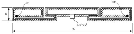
- FIG. 10 is a plan view showing the shape of the dipole antenna used in Example 2; It is a top view which shows the shape of the dipole antenna used for Example 3 and Comparative Example 2.
- FIG. 16 is a plan view showing the shape of the dipole antenna used in Example 4;
- FIG. 18 is a plan view showing the shape of the dipole antenna used in Example 5;
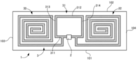
- FIG. 1 is a plan view of the IC tag according to the present embodiment
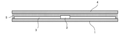
- FIG. 2 is a cross-sectional view of FIG.
- the cover is abbreviate
- the IC tag according to the present embodiment includes a sheet-like base material 1 formed in a rectangular shape, an IC chip 2 and a dipole antenna 3 disposed on the base material 1. And a rectangular sheet-like cover 4 covering the IC chip 2 and the dipole antenna 3.
- the base 1 and the cover 4 are adhered by an adhesive 5.
- each of these members will be described in detail.
- the base 1 and the cover 4 are formed in the same shape, and the adhesive 5 is disposed over the entire surface between them. That is, the IC chip 2 and the dipole antenna 3 are covered with the adhesive 5, and the IC chip 2 and the dipole antenna 3 are not exposed from the gap between the base 1 and the cover 4.
- the material which comprises the base material 1 and the cover 4 is not specifically limited, For example, it can form with polyethylene, a polypropylene, a polyethylene terephthalate, a polyvinyl chloride etc.
- the thickness of the substrate 1 and the cover 4 is preferably 25 to 200 ⁇ m, for example, and more preferably 25 to 100 ⁇ m.
- the sides in the longitudinal direction of the base material 1 and the cover 4 are referred to as the first side 101 and the second side 102, and the sides in the lateral direction are the third.
- the side 103 and the fourth side 104 will be referred to. Therefore, these sides are connected in the order of the first side 101, the third side 103, the second side 102, and the fourth side 104.
- the IC chip 2 is a known one having a memory function, and is electrically connected to a dipole antenna 3 formed of a conductor.
- a dipole antenna as shown in FIG. 1 is used as an example. That is, the dipole antenna 3 includes an impedance matching portion 31 disposed near the center of the base 1 in the longitudinal direction, and a pair of dipole portions 32 extending from the impedance matching portion 31 in the longitudinal direction of the base 1. ing.
- the impedance matching portion 31 is formed in a rectangular frame shape having first to fourth sides. More specifically, the first side 311 of the impedance matching portion 31 is disposed at a position slightly away from the first side 101 of the base 1, and the second side 312 is along the second side 102 of the base 1. It is arranged.
- the first side 311, the third side 313, the second side 312, and the fourth side 314 are connected in this order.
- the IC chip 2 is disposed near the center of the first side 311 of the impedance matching unit 31.
- the dipole section 32 has a symmetrical shape, so only one will be described.
- the dipole section 32 extends from the first side 311 in the impedance matching section 31 to the first side 101 side of the base material 1, and from there to the first side 101, the third side 103, and the second side 102 of the base material 1.
- the rectangular frame extends along the third side 313 of the impedance matching portion 31 and then extends in a spiral manner inside the frame.
- the material which comprises the dipole antenna 3 is not specifically limited, For example, it can form with silver, copper, aluminum.
- the dipole antenna 3 can be formed by applying a silver paste containing silver onto the substrate 1 by screen printing.
- the dipole antenna 3 can be formed by etching.
- the IC chip 2 can be fixed to the antenna 3 by, for example, known flip chip mounting for electronic components.
- the dipole antenna 3 as described above can transmit and receive information stored in the IC chip 2 by radio waves in the UHF band, for example.
- the pressure-sensitive adhesive 5 can be, for example, a rubber-based pressure-sensitive adhesive containing natural rubber or synthetic rubber as a main component.
- the thickness of the rubber-based pressure-sensitive adhesive 5 is not particularly limited, but is preferably 28 to 500 ⁇ m, and more preferably 28 to 72 ⁇ m.
- the synthetic rubber used for the rubber-based pressure-sensitive adhesive 5 is not particularly limited, but, for example, styrene-isoprene-styrene block copolymer, styrene-butadiene-styrene block copolymer, hydrogenation of the styrene-based block copolymer , Styrene-butadiene rubber (SBR), polyisoprene rubber (IR), polyisobutylene (PIB), butyl rubber (IIR) and the like.
- SBR Styrene-butadiene rubber
- IR polyisoprene rubber
- PIB polyisobutylene
- IIR butyl rubber
- the rubber-based pressure-sensitive adhesive 5 may contain a tackifier.
- tackifiers include terpene phenol resins, rosin resins, petroleum resins and the like.
- the amount of tackifier resin used can be appropriately selected within the range that does not impair the adhesion performance.
- the rubber-based pressure-sensitive adhesive may contain, if necessary, appropriate additives such as a softener, a plasticizer, a filler, an antiaging agent, and a colorant.
- an acrylic or silicone-based pressure-sensitive adhesive can also be used as the pressure-sensitive adhesive 5.
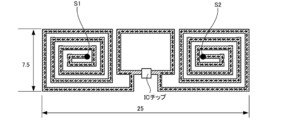
- the dipole antenna 3 according to the present embodiment has the following physical properties and electrical characteristics. This point will be described with reference to FIG. As shown in the figure, first, the resistance value R ( ⁇ ) between both ends S1 and S2 of the dipole antenna 3 and the length of the path connecting the both ends S1 and S2 of the dipole antenna 3 along the dipole antenna 3 When the length L (cm) of the path (hereinafter referred to as antenna path: broken line in FIG. 3) which does not pass through the IC chip 2 is set, the dipole antenna 3 according to this embodiment Satisfy 1).
- the antenna path is a path passing through the center of the line width of the dipole antenna 1. 0.1 ⁇ R / L ⁇ 2.5 (1)
- R / L is 0.1 or more, the current hardly flows, so that detection by the metal detector is prevented.
- R / L is preferably 2.5 or less.
- R / L it is more preferable that R / L satisfy the following expression (2). 1.5 ⁇ R / L ⁇ 2.5 (2)
- the resistance value R ( ⁇ ) between the end portions S1 and S2 of the antenna 3 is not particularly limited, but is preferably 10 to 50 ⁇ , and more preferably 20 to 44 ⁇ . This is because if the resistance value R is 10 ⁇ or more, the current hardly flows. If the resistance value R is 50 ⁇ or less, the communication distance becomes long, and the communication is stabilized.
- the length L of the antenna path described above is also not particularly limited, but is preferably 120 to 200 mm, for example, and preferably 130 to 180 mm. This is because when the length L of the antenna path is short, communication becomes unstable, and when the length of the antenna path is too long, it becomes easy to be detected by the metal detector.
- the size of the outer shape of the dipole antenna 3 is not particularly limited, but in order to prevent detection by the metal detector, for example, the length X in the longitudinal direction of the outer shape of the dipole antenna 3 is 60 mm or less Preferably, it is 40 mm or less.
- the length Y in the short direction of the outer shape of the dipole antenna 3 is preferably 20 mm or less, and more preferably 10 mm or less. Therefore, the area (X * Y) of the outer shape of the dipole antenna is preferably 1200 mm 2 , and more preferably 400 mm 2 or less.
- the thickness of the dipole antenna 3 is not particularly limited, for example, it is preferably 20 ⁇ m or less, more preferably 15 ⁇ m or less, and particularly preferably 10 ⁇ m or less.
- the dipole antenna 3 is formed by printing using the silver paste described above, adjustment of the thickness of the dipole antenna 3 becomes easier than forming the dipole antenna 3 by etching using copper or aluminum, and is 10 ⁇ m or less It can be thick. This can further prevent detection by the metal detector.
- the metal detector which assumes that the IC tag which concerns on this embodiment is not detected can be used as the metal detector which detects nonferrous metal, for example. This is because, as described above, the dipole antenna may be formed of non-ferrous metals such as silver, copper, and aluminum.
- the detection sensitivity is preferably not detected when, for example, MUK-500 manufactured by Nikka Densetsu Co., Ltd. is used as a metal detector. This device has a detection sensitivity that can detect a SUS ball with an outer diameter of 1.5 mm or more as the smallest detectable substance.
- a metal detector in which the IC tag according to the present embodiment is not detected a metal detector having the above detection sensitivity to non-ferrous metal can be defined.
- this is an example, and it can also be based on a metal detector that detects iron.
- the shape of the dipole antenna 3 described above is an example, and may be various shapes as long as the above equation (1) is satisfied.
- the shape of the IC tag that is, the shapes of the base 1 and the cover 4 is not particularly limited, and various other shapes such as a rectangular shape, a circular shape, and a polygonal shape besides the above long shape. It can be shaped. Further, the base 1 and the cover 4 may not have the same shape.
- the adhesive 5 is apply
- the rubber-based pressure-sensitive adhesive 5 may be applied only to the periphery of the base 1 and the cover 4 so that the IC chip 2 and the antenna 3 are surrounded by the pressure-sensitive adhesive 5.
- the cover 4 and the adhesive 5 are not essential, and may not be provided.
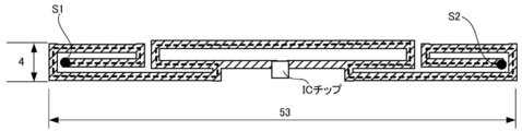
- IC tags according to Examples 1 to 5 and Comparative Examples 1 and 2 were prepared as follows. In these examples and comparative examples, the substrate and the IC chip are the same but the dipole antenna is different. Here, five types of antenna shapes shown in FIGS. 4 to 8 were prepared, and three types of materials were prepared. The dotted lines in FIG. 4 to FIG. 8 indicate the path L, and the numerical values indicate the lengths X and Y of the outline. In addition, a polyethylene terephthalate film having a thickness of 50 ⁇ m was prepared as a substrate and a cover, a dipole antenna was disposed between the substrate and the cover, and fixed with the above-described rubber-based pressure-sensitive adhesive. Then, the IC tags according to Examples 1 to 5 and Comparative Examples 1 and 2 were prepared as shown in Table 1 below. As described below, the antennas of the example and the comparative example are made of nonferrous metals.
- the detection level in this device is 0-12. Specifically, it is as follows. That is, when using a SUS304 ball, this device can not detect a ball with a diameter of 1 mm, but can detect a ball with a diameter of 2 mm or more. The detection level is 8 when a ball with a diameter of 2 mm is detected, and 12 when a ball with a diameter of 3 mm is detected. On the other hand, a detection level of 0 means that this metal detector can not detect at all. That is, the closer the detection level is to 0, the more impossibility of detection by this metal detector.
- R / L was 1.5 or more, and the detection levels were all 0. That is, it was not detected at all by the metal detector.
- R / L was lower than Examples 1 to 3 and was 1 or less, but was 0.1 or more.
- the detection level by the metal detector was 3. That is, although at a slight level, it is detected but usable for some applications.
- R / L was lower than 0.1, and the detection level was 12. That is, it is a level that can be reliably detected by the metal detector. Therefore, in the evaluation based on R / L, it was found that Examples 1 to 5 were all superior to Comparative Examples 1 and 2.
Landscapes
- Engineering & Computer Science (AREA)
- Physics & Mathematics (AREA)
- General Physics & Mathematics (AREA)
- Theoretical Computer Science (AREA)
- Computer Hardware Design (AREA)
- Microelectronics & Electronic Packaging (AREA)
- Computer Networks & Wireless Communication (AREA)
- Details Of Aerials (AREA)
- Support Of Aerials (AREA)
- Credit Cards Or The Like (AREA)
Abstract
Description
以下、本発明に係るICタグの一実施形態について、図面を参照しつつ説明する。図1は、本実施形態に係るICタグの平面図、図2は図1の断面図である。但し、図1は説明の便宜のため、カバーを省略している。図1及び図2に示すように、本実施形態に係るICタグは、矩形状に形成されたシート状の基材1と、この基材1上に配置されたICチップ2及びダイポールアンテナ3と、これらICチップ2及びダイポールアンテナ3を覆う矩形状に形成されたシート状のカバー4と、を備えている。そして、基材1とカバー4とは、粘着剤5によって接着されている。以下、これら各部材について詳細に説明する。
本実施形態に係るダイポールアンテナ3は、次のような物性及び電気特性を有している。この点について、図3を参照しつつ説明する。同図に示すように、まず、ダイポールアンテナ3の両端部S1,S2間の抵抗値R(Ω)、及び、このダイポールアンテナ3に沿ってダイポールアンテナ3の両端部S1,S2を繋ぐ経路の長さであって、ICチップ2を通過しない経路(以下、アンテナ経路という:図3の破線)の長さL(cm)を設定したとき、本実施形態に係るダイポールアンテナ3は、以下の式(1)を充足する。なお、アンテナ経路は、ダイポールアンテナ1の線幅の中心を通る経路である。
0.1≦R/L≦2.5 (1)
1.5≦R/L≦2.5 (2)
本実施形態に係るICタグが検出されないことを想定する金属探知機は、例えば、非鉄金属を検出する金属探知機とすることができる。これは、上記のように、ダイポールアンテナが銀、銅、アルミニウム等の非鉄金属で形成されることがあることによる。そして、検出感度としては、例えば、金属探知機として、ニッカ電測株式会社のMUK-500を用いたときに、検出されないことが好ましい。この装置は、検出できる最小の物質として、外径が1.5mm以上のSUSの球を検出できる検出感度を有している。したがって、一例として、本実施形態に係るICタグが検出されない金属探知機として、非鉄金属に対し、上記のような検出感度を有する金属探知機を規定することができる。但し、これは一例であり、鉄を検出する金属探知機を基準とすることもできる。
以上のように、本実施形態に係るICタグによれば、ダイポールアンテナ3が上記式(1)を充足するように構成されているため、金属探知機で検出されるのを防止することができる。
以上、本発明の一実施形態について説明したが、本発明は上記実施形態に限定されるものではなく、その趣旨を逸脱しない限りにおいて、種々の変更が可能である。そして、以下に示す複数の変形例は適宜組合わせることが可能である。
上述したダイポールアンテナ3の形状は、一例であり、上記式(1)を充足する限りは、種々の形状にすることができる。また、ICタグの形状、つまり、基材1やカバー4の形状も特には限定されず、上記のような長尺状のほか、矩形状、円形状、多角形状など、用途に合わせて種々の形状にすることができる。また、基材1とカバー4とを同形状にしなくてもよい。
上記実施形態では、基材1とカバー4との間の全面に亘って、粘着剤5が塗布されているが、これに限定されるものではない。例えば、基材1とカバー4の周縁にのみゴム系粘着剤5を塗布し、ICチップ2及びアンテナ3が粘着剤5によって囲まれるようにすることもできる。また、カバー4及び粘着剤5は、必須ではなく、設けないようにすることもできる。
以下のように、実施例1~5及び比較例1,2に係るICタグを準備した。これら実施例及び比較例において、基材及びICチップは同じであるが、ダイポールアンテナが相違している。ここでは、図4~図8に示す5種類のアンテナ形状を準備し、3種類の材料を準備した。図4~図8の点線は経路Lであり、数値は外形の長さX,Yを示している。また、基材及びカバーとして、厚みが50μmのポリエチレンテレフタレートフィルムを準備し、ダイポールアンテナを基材とカバーとの間に配置し、上述したゴム系粘着剤により固定した。そして、実施例1~5及び比較例1,2に係るICタグを以下の表1に示すように準備した。以下のように、実施例及び比較例のアンテナは非鉄金属で構成されている。

金属探知機として、ニッカ電測株式会社製MUK-500を用い、上記実施例及び比較例を検知できるかを試験した。この装置における検知レベルは0~12である。具体的には次の通りである。すなわち、SUS304の球を用いた場合、この装置では、直径が1mmの球は検知できないが、直径2mm以上の球が検知できる。そして、直径2mmの球を検知したときの検知レベルは8であり、直径3mmの球を検知したときの検知レベルは12である。一方、検知レベルが0とは、この金属探知機での検出が全くできないことを意味する。すなわち、検知レベルが0に近いほど、この金属探知機での検出ができなくなることを意味する。

2 ICチップ
3 ダイポールアンテナ
4 カバー
5 粘着剤
Claims (4)
- ICチップと、
前記ICチップに格納された情報を電気的に送受信するダイポールアンテナと、
前記ICチップ及びダイポールアンテナを支持するシート状の基材と、
を備え、
前記ダイポールアンテナの両端部間の抵抗値R、及び、前記ダイポールアンテナに沿って当該ダイポールアンテナの両端部を繋ぐ経路の長さであって、前記ICチップを通過しない経路の長さLを設定したとき、0.1≦R/L≦2.5を充足する、ICタグ。 - 前記長さLが、120mm以上200mm以下である、請求項1に記載のICタグ。
- 前記ダイポールアンテナを構成する材料は、銀、アルミニウム、及び銅のいずれかを含有する、請求項1または2に記載のICタグ。
- 前記基材との間で、前記ICチップ及びアンテナを覆うシート状のカバーと、
前記カバーと基材とを接着する粘着剤と、
をさらに備えている、請求項1から3のいずれかに記載のICタグ。
Priority Applications (5)
| Application Number | Priority Date | Filing Date | Title |
|---|---|---|---|
| EP18898329.0A EP3736738B1 (en) | 2018-01-05 | 2018-12-27 | Ic tag |
| CA3087661A CA3087661A1 (en) | 2018-01-05 | 2018-12-27 | Ic tag |
| CN201880085199.9A CN111566670B (zh) | 2018-01-05 | 2018-12-27 | Ic标签 |
| US16/959,840 US12307313B2 (en) | 2018-01-05 | 2018-12-27 | IC tag |
| KR1020207018948A KR20200105479A (ko) | 2018-01-05 | 2018-12-27 | Ic 태그 |
Applications Claiming Priority (2)
| Application Number | Priority Date | Filing Date | Title |
|---|---|---|---|
| JP2018000866A JP6976865B2 (ja) | 2018-01-05 | 2018-01-05 | Icタグ |
| JP2018-000866 | 2018-01-05 |
Publications (1)
| Publication Number | Publication Date |
|---|---|
| WO2019135381A1 true WO2019135381A1 (ja) | 2019-07-11 |
Family
ID=67144136
Family Applications (1)
| Application Number | Title | Priority Date | Filing Date |
|---|---|---|---|
| PCT/JP2018/048003 Ceased WO2019135381A1 (ja) | 2018-01-05 | 2018-12-27 | Icタグ |
Country Status (7)
| Country | Link |
|---|---|
| US (1) | US12307313B2 (ja) |
| EP (1) | EP3736738B1 (ja) |
| JP (1) | JP6976865B2 (ja) |
| KR (1) | KR20200105479A (ja) |
| CN (1) | CN111566670B (ja) |
| CA (1) | CA3087661A1 (ja) |
| WO (1) | WO2019135381A1 (ja) |
Families Citing this family (4)
| Publication number | Priority date | Publication date | Assignee | Title |
|---|---|---|---|---|
| JP7624005B2 (ja) * | 2019-12-30 | 2025-01-29 | エイヴェリー デニソン リテール インフォメーション サービシズ リミテッド ライアビリティ カンパニー | 金属探知機耐性rfidタグ |
| JP7587979B2 (ja) * | 2020-12-17 | 2024-11-21 | 大王製紙株式会社 | Rfidタグ及びその製造方法 |
| DE102021004810A1 (de) | 2021-09-23 | 2023-03-23 | Giesecke+Devrient Mobile Security Gmbh | Kartenförmiger Datenträger und Verfahren zum Lösen einer Klebeverbindung für einen kartenförmigen Datenträger |
| WO2024194937A1 (ja) | 2023-03-17 | 2024-09-26 | 富士通フロンテック株式会社 | Rfidタグ |
Citations (2)
| Publication number | Priority date | Publication date | Assignee | Title |
|---|---|---|---|---|
| JP2006197440A (ja) * | 2005-01-17 | 2006-07-27 | Toppan Printing Co Ltd | アンテナ回路導体、及び非接触icタグ |
| JP2016033748A (ja) | 2014-07-31 | 2016-03-10 | トッパン・フォームズ株式会社 | 非接触型データ受送信体 |
Family Cites Families (13)
| Publication number | Priority date | Publication date | Assignee | Title |
|---|---|---|---|---|
| US6816125B2 (en) * | 2003-03-01 | 2004-11-09 | 3M Innovative Properties Company | Forming electromagnetic communication circuit components using densified metal powder |
| US7804411B2 (en) * | 2004-11-15 | 2010-09-28 | Sensormatic Electronics, LLC | Combination EAS and RFID label or tag using a hybrid RFID antenna |
| KR20100021665A (ko) * | 2004-12-14 | 2010-02-25 | 후지쯔 가부시끼가이샤 | 안테나 및 비접촉형 태그 |
| US7714794B2 (en) | 2005-01-19 | 2010-05-11 | Behzad Tavassoli Hozouri | RFID antenna |
| EP1887497B1 (en) * | 2006-08-10 | 2015-05-27 | Fujitsu Limited | RFID tag |
| DE102006055744A1 (de) * | 2006-11-25 | 2008-05-29 | Atmel Germany Gmbh | Antenne für einen rückstreubasierten RFID-Transponder |
| JP5018884B2 (ja) | 2007-07-18 | 2012-09-05 | 富士通株式会社 | 無線タグ及び無線タグの製造方法 |
| EP2073307A1 (en) * | 2007-12-21 | 2009-06-24 | Fujitsu Ltd. | Automatic antenna designing apparatus and automatic antenna designing method |
| JP4518211B2 (ja) * | 2008-03-03 | 2010-08-04 | 株式会社村田製作所 | 複合アンテナ |
| CN102498617B (zh) * | 2009-09-09 | 2015-04-01 | 株式会社村田制作所 | 天线及其制造方法、以及无线ic器件 |
| JP2015008444A (ja) * | 2013-06-26 | 2015-01-15 | 凸版印刷株式会社 | ブースタ付きicタグ |
| JP6860308B2 (ja) | 2016-08-31 | 2021-04-14 | 大王製紙株式会社 | パンツタイプ使い捨ておむつ |
| CN107358291B (zh) * | 2017-08-25 | 2023-05-23 | 昆山法拉第智能科技有限公司 | 一种具有高测试灵敏度的电子标签 |
-
2018
- 2018-01-05 JP JP2018000866A patent/JP6976865B2/ja active Active
- 2018-12-27 US US16/959,840 patent/US12307313B2/en active Active
- 2018-12-27 WO PCT/JP2018/048003 patent/WO2019135381A1/ja not_active Ceased
- 2018-12-27 EP EP18898329.0A patent/EP3736738B1/en active Active
- 2018-12-27 CA CA3087661A patent/CA3087661A1/en active Pending
- 2018-12-27 KR KR1020207018948A patent/KR20200105479A/ko not_active Ceased
- 2018-12-27 CN CN201880085199.9A patent/CN111566670B/zh active Active
Patent Citations (2)
| Publication number | Priority date | Publication date | Assignee | Title |
|---|---|---|---|---|
| JP2006197440A (ja) * | 2005-01-17 | 2006-07-27 | Toppan Printing Co Ltd | アンテナ回路導体、及び非接触icタグ |
| JP2016033748A (ja) | 2014-07-31 | 2016-03-10 | トッパン・フォームズ株式会社 | 非接触型データ受送信体 |
Non-Patent Citations (1)
| Title |
|---|
| See also references of EP3736738A4 |
Also Published As
| Publication number | Publication date |
|---|---|
| EP3736738B1 (en) | 2025-01-22 |
| EP3736738A1 (en) | 2020-11-11 |
| US20200372314A1 (en) | 2020-11-26 |
| KR20200105479A (ko) | 2020-09-07 |
| US12307313B2 (en) | 2025-05-20 |
| CN111566670B (zh) | 2023-07-14 |
| CN111566670A (zh) | 2020-08-21 |
| JP2019121933A (ja) | 2019-07-22 |
| EP3736738A4 (en) | 2021-09-15 |
| CA3087661A1 (en) | 2019-07-11 |
| JP6976865B2 (ja) | 2021-12-08 |
Similar Documents
| Publication | Publication Date | Title |
|---|---|---|
| WO2019135381A1 (ja) | Icタグ | |
| TWI301947B (en) | Rfid tag | |
| JP6265203B2 (ja) | 容器 | |
| JP4453582B2 (ja) | Rfidタグ | |
| FI111881B (fi) | Älykorttiraina ja menetelmä sen valmistamiseksi | |
| US20220076093A1 (en) | Rfid label and rfid tag | |
| US20070182560A1 (en) | Wireless tag and method of reading data from a wireless tag | |
| JP2019016330A (ja) | Rfidタグラベルおよびrfidタグラベル連続体 | |
| JP2023502687A (ja) | Rfidラベル | |
| JP2003188765A (ja) | Rfid用タグ及び共振周波数の調節方法並びに共振周波数調整装置 | |
| CN112449702B (zh) | Ic标签 | |
| CN114746916A (zh) | 磁标识器 | |
| JP2006127424A (ja) | 無線タグ | |
| JP7084269B2 (ja) | 非接触通信媒体 | |
| CN202838391U (zh) | 电子标签 | |
| TW201403948A (zh) | 環形天線用屏蔽材、屏蔽單元、及屏蔽標籤 | |
| JP2019175195A (ja) | Icタグ | |
| JP7176226B2 (ja) | Rfタグラベルおよびrfタグ構造体 | |
| JP7014027B2 (ja) | Rfタグラベルおよびrfタグ構造体 | |
| JP7407044B2 (ja) | 亀裂検知ラベルセット | |
| JP2007243468A (ja) | 非接触式データキャリア用磁性体シート及びこれを用いた非接触式データキャリア | |
| KR101572072B1 (ko) | 캐리어 밴드용 복합 커넥팅 테이프 | |
| US20070126580A1 (en) | Apparatus and method for reducing the risk of static induced damage of an radio frequency identification device | |
| JP4636549B2 (ja) | 車載フィルムアンテナ | |
| JP6998787B2 (ja) | Icタグ |
Legal Events
| Date | Code | Title | Description |
|---|---|---|---|
| 121 | Ep: the epo has been informed by wipo that ep was designated in this application |
Ref document number: 18898329 Country of ref document: EP Kind code of ref document: A1 |
|
| ENP | Entry into the national phase |
Ref document number: 3087661 Country of ref document: CA |
|
| NENP | Non-entry into the national phase |
Ref country code: DE |
|
| ENP | Entry into the national phase |
Ref document number: 2018898329 Country of ref document: EP Effective date: 20200805 |
|
| WWG | Wipo information: grant in national office |
Ref document number: 16959840 Country of ref document: US |
|
| WWR | Wipo information: refused in national office |
Ref document number: 1020207018948 Country of ref document: KR |