WO2019139020A1 - Cellule solaire et procédé de fabrication de cellule solaire - Google Patents
Cellule solaire et procédé de fabrication de cellule solaire Download PDFInfo
- Publication number
- WO2019139020A1 WO2019139020A1 PCT/JP2019/000285 JP2019000285W WO2019139020A1 WO 2019139020 A1 WO2019139020 A1 WO 2019139020A1 JP 2019000285 W JP2019000285 W JP 2019000285W WO 2019139020 A1 WO2019139020 A1 WO 2019139020A1
- Authority
- WO
- WIPO (PCT)
- Prior art keywords
- underlayer
- semiconductor layer
- type semiconductor
- laser
- separation
- Prior art date
- Legal status (The legal status is an assumption and is not a legal conclusion. Google has not performed a legal analysis and makes no representation as to the accuracy of the status listed.)
- Ceased
Links
Images





Classifications
-
- H—ELECTRICITY
- H10—SEMICONDUCTOR DEVICES; ELECTRIC SOLID-STATE DEVICES NOT OTHERWISE PROVIDED FOR
- H10F—INORGANIC SEMICONDUCTOR DEVICES SENSITIVE TO INFRARED RADIATION, LIGHT, ELECTROMAGNETIC RADIATION OF SHORTER WAVELENGTH OR CORPUSCULAR RADIATION
- H10F77/00—Constructional details of devices covered by this subclass
- H10F77/20—Electrodes
- H10F77/206—Electrodes for devices having potential barriers
- H10F77/211—Electrodes for devices having potential barriers for photovoltaic cells
- H10F77/219—Arrangements for electrodes of back-contact photovoltaic cells
-
- H—ELECTRICITY
- H10—SEMICONDUCTOR DEVICES; ELECTRIC SOLID-STATE DEVICES NOT OTHERWISE PROVIDED FOR
- H10F—INORGANIC SEMICONDUCTOR DEVICES SENSITIVE TO INFRARED RADIATION, LIGHT, ELECTROMAGNETIC RADIATION OF SHORTER WAVELENGTH OR CORPUSCULAR RADIATION
- H10F10/00—Individual photovoltaic cells, e.g. solar cells
- H10F10/10—Individual photovoltaic cells, e.g. solar cells having potential barriers
- H10F10/14—Photovoltaic cells having only PN homojunction potential barriers
- H10F10/146—Back-junction photovoltaic cells, e.g. having interdigitated base-emitter regions on the back side
-
- H—ELECTRICITY
- H10—SEMICONDUCTOR DEVICES; ELECTRIC SOLID-STATE DEVICES NOT OTHERWISE PROVIDED FOR
- H10F—INORGANIC SEMICONDUCTOR DEVICES SENSITIVE TO INFRARED RADIATION, LIGHT, ELECTROMAGNETIC RADIATION OF SHORTER WAVELENGTH OR CORPUSCULAR RADIATION
- H10F10/00—Individual photovoltaic cells, e.g. solar cells
- H10F10/10—Individual photovoltaic cells, e.g. solar cells having potential barriers
- H10F10/16—Photovoltaic cells having only PN heterojunction potential barriers
- H10F10/164—Photovoltaic cells having only PN heterojunction potential barriers comprising heterojunctions with Group IV materials, e.g. ITO/Si or GaAs/SiGe photovoltaic cells
- H10F10/165—Photovoltaic cells having only PN heterojunction potential barriers comprising heterojunctions with Group IV materials, e.g. ITO/Si or GaAs/SiGe photovoltaic cells the heterojunctions being Group IV-IV heterojunctions, e.g. Si/Ge, SiGe/Si or Si/SiC photovoltaic cells
- H10F10/166—Photovoltaic cells having only PN heterojunction potential barriers comprising heterojunctions with Group IV materials, e.g. ITO/Si or GaAs/SiGe photovoltaic cells the heterojunctions being Group IV-IV heterojunctions, e.g. Si/Ge, SiGe/Si or Si/SiC photovoltaic cells the Group IV-IV heterojunctions being heterojunctions of crystalline and amorphous materials, e.g. silicon heterojunction [SHJ] photovoltaic cells
-
- H—ELECTRICITY
- H10—SEMICONDUCTOR DEVICES; ELECTRIC SOLID-STATE DEVICES NOT OTHERWISE PROVIDED FOR
- H10F—INORGANIC SEMICONDUCTOR DEVICES SENSITIVE TO INFRARED RADIATION, LIGHT, ELECTROMAGNETIC RADIATION OF SHORTER WAVELENGTH OR CORPUSCULAR RADIATION
- H10F19/00—Integrated devices, or assemblies of multiple devices, comprising at least one photovoltaic cell covered by group H10F10/00, e.g. photovoltaic modules
- H10F19/30—Integrated devices, or assemblies of multiple devices, comprising at least one photovoltaic cell covered by group H10F10/00, e.g. photovoltaic modules comprising thin-film photovoltaic cells
-
- H—ELECTRICITY
- H10—SEMICONDUCTOR DEVICES; ELECTRIC SOLID-STATE DEVICES NOT OTHERWISE PROVIDED FOR
- H10F—INORGANIC SEMICONDUCTOR DEVICES SENSITIVE TO INFRARED RADIATION, LIGHT, ELECTROMAGNETIC RADIATION OF SHORTER WAVELENGTH OR CORPUSCULAR RADIATION
- H10F19/00—Integrated devices, or assemblies of multiple devices, comprising at least one photovoltaic cell covered by group H10F10/00, e.g. photovoltaic modules
- H10F19/90—Structures for connecting between photovoltaic cells, e.g. interconnections or insulating spacers
-
- H—ELECTRICITY
- H10—SEMICONDUCTOR DEVICES; ELECTRIC SOLID-STATE DEVICES NOT OTHERWISE PROVIDED FOR
- H10F—INORGANIC SEMICONDUCTOR DEVICES SENSITIVE TO INFRARED RADIATION, LIGHT, ELECTROMAGNETIC RADIATION OF SHORTER WAVELENGTH OR CORPUSCULAR RADIATION
- H10F77/00—Constructional details of devices covered by this subclass
- H10F77/20—Electrodes
- H10F77/244—Electrodes made of transparent conductive layers, e.g. transparent conductive oxide [TCO] layers
-
- H—ELECTRICITY
- H10—SEMICONDUCTOR DEVICES; ELECTRIC SOLID-STATE DEVICES NOT OTHERWISE PROVIDED FOR
- H10W—GENERIC PACKAGES, INTERCONNECTIONS, CONNECTORS OR OTHER CONSTRUCTIONAL DETAILS OF DEVICES COVERED BY CLASS H10
- H10W10/00—Isolation regions in semiconductor bodies between components of integrated devices
-
- H—ELECTRICITY
- H10—SEMICONDUCTOR DEVICES; ELECTRIC SOLID-STATE DEVICES NOT OTHERWISE PROVIDED FOR
- H10W—GENERIC PACKAGES, INTERCONNECTIONS, CONNECTORS OR OTHER CONSTRUCTIONAL DETAILS OF DEVICES COVERED BY CLASS H10
- H10W10/00—Isolation regions in semiconductor bodies between components of integrated devices
- H10W10/01—Manufacture or treatment
-
- Y—GENERAL TAGGING OF NEW TECHNOLOGICAL DEVELOPMENTS; GENERAL TAGGING OF CROSS-SECTIONAL TECHNOLOGIES SPANNING OVER SEVERAL SECTIONS OF THE IPC; TECHNICAL SUBJECTS COVERED BY FORMER USPC CROSS-REFERENCE ART COLLECTIONS [XRACs] AND DIGESTS
- Y02—TECHNOLOGIES OR APPLICATIONS FOR MITIGATION OR ADAPTATION AGAINST CLIMATE CHANGE
- Y02E—REDUCTION OF GREENHOUSE GAS [GHG] EMISSIONS, RELATED TO ENERGY GENERATION, TRANSMISSION OR DISTRIBUTION
- Y02E10/00—Energy generation through renewable energy sources
- Y02E10/50—Photovoltaic [PV] energy
- Y02E10/547—Monocrystalline silicon PV cells
Definitions
- the present invention relates to a back contact solar cell, and a method of manufacturing the solar cell.
- a back surface junction type in which both an n-type semiconductor layer and a p-type semiconductor layer are formed on the back surface which is a surface opposite to the light receiving surface of the semiconductor substrate A study of solar cells is being conducted.
- a transparent electrode layer base layer
- a seed layer conductive layer
- a plating layer n-side electrode and p-side electrode
- Patent Document 1 discloses a solar battery cell in which an n-side electrode and a p-side electrode are completely separated by a separation region (separation groove) provided in a transparent electrode layer.
- the process by a laser may be performed as a method of forming a separating groove in a base layer.
- the underlayer is completely separated by the separation groove
- the patterning by the laser there are places where the scanning paths intersect. If the laser is illuminated while scanning the laser in the scan path, there will be places where the laser is over-illuminated. As a result, the semiconductor layer and the semiconductor substrate may be damaged and the photoelectric conversion efficiency may be reduced.
- this invention aims at providing the manufacturing method of the photovoltaic cell by which the damage to a semiconductor layer etc. was suppressed when the process by a laser is performed, and a photovoltaic cell.
- a solar battery cell is a back surface contact type solar battery cell, and has a light receiving surface on which light is incident and a back surface opposite to the light receiving surface.
- a method of manufacturing a solar battery cell is a method of manufacturing a back surface contact type solar battery cell, having a light receiving surface on which light is incident, and a back surface opposite to the light receiving surface.
- the output of the laser is stopped at a position where the scanning path scanned the laser intersects the first separation portion and the second portion which extend in different directions at the position.
- the separation groove separated from the separation portion is formed.
- FIG. 1 is a plan view showing the solar battery cell according to Embodiment 1.
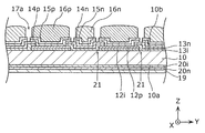
- FIG. FIG. 2 is a partial cross-sectional view of the solar battery cell according to the first embodiment, taken along line II-II in FIG.
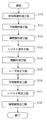
- FIG. 3 is a flowchart showing a method of manufacturing the solar battery cell according to the first embodiment.
- FIG. 4 is a schematic cross-sectional view after the electrode forming step of the solar battery cell according to the first embodiment.
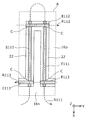
- FIG. 5A is a plan view showing a scanning path of a laser in a laser processing process according to a comparative example.
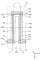
- FIG. 5B is a plan view showing the scanning path of the laser in the laser processing process according to the first embodiment.
- FIG. 6A is a partial cross-sectional view of the solar battery cell in the manufacturing process according to Embodiment 1, taken along line VIa-VIa of FIG. 5B.
- 6B is a partial cross-sectional view of the solar battery cell in the manufacturing process according to Embodiment 1, taken along line VIb-VIb in FIG. 5B.
- FIG. 7A is a partial cross-sectional view after the underlayer removing step of the solar battery cell in accordance with Embodiment 1 at a position corresponding to the line VIa-VIa in FIG. 5B.
- FIG. 7B is a partial cross-sectional view after the underlayer removing step of the solar battery cell in accordance with Embodiment 1 at a position corresponding to the VIb-VIb line in FIG. 5B.
- FIG. 8 is a partial cross-sectional view of the solar battery cell according to the first embodiment after the conductive layer removing step.
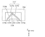
- FIG. 9 is a plan view showing a solar battery cell according to a first modification of the first embodiment.
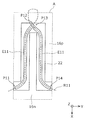
- FIG. 10 is a plan view showing a scanning path of a laser in a laser processing step according to Modification 1 of Embodiment 1.
- FIG. 11 is a plan view showing a scanning path of a laser in a laser processing step according to Modification 2 of Embodiment 1.
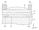
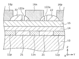
- 12A is a partial cross-sectional view of the solar battery cell according to Variation 2 of Embodiment 1 after the laser processing step, taken along line XIIa-XIIa of FIG.
- FIG. 12B is a partial cross-sectional view of the XIIb-XIIb line of FIG. 11 after the laser processing step of the solar battery cell according to the second modification of the first embodiment.
- FIG. 13 is a partial cross-sectional view of the solar battery cell according to the second modification of the first embodiment after the conductive layer removing step.
- FIG. 14 is a partial cross-sectional view of the solar battery cell according to the third modification of the first embodiment.
- FIG. 15 is a plan view showing the scanning path of the laser in the vicinity of the short side of the solar battery cell in the first embodiment.
- FIG. 16 is an enlarged view of a region C in FIG.
- the Z-axis direction is, for example, a direction perpendicular to the light receiving surface of the solar battery cell.
- the X axis direction and the Y axis direction are orthogonal to each other, and both are directions orthogonal to the Z axis direction.
- plane view means viewing from the Z-axis direction.
- cross-sectional view refers to cutting of the solar battery cell in a plane orthogonal to the light receiving surface of the solar battery cell (for example, a plane defined by the Z axis and the X axis) It means that the face is viewed from a direction (for example, the Y-axis direction) substantially orthogonal to the cutting plane.
- Embodiment 1 The solar cell according to the present embodiment will be described below with reference to FIGS. 1 to 8.
- a photovoltaic cell is a photoelectric conversion element (photovoltaic element) that converts light such as sunlight into electric power.
- FIG. 1 is a plan view showing a solar battery cell 1 according to the present embodiment.
- FIG. 1 is a plan view of the solar battery cell 1 as viewed from the back side.
- (a) of FIG. 1 is a plan view showing the solar battery cell 1 according to the present embodiment
- (b) of FIG. 1 is an enlarged plane of a broken line frame of (a) of FIG.
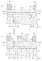
- FIG. 2 is a partial cross-sectional view of solar cell 1 according to the present embodiment, taken along line II-II in FIG. 1 (a).
- the light receiving surface 10 a on which light is incident is illustrated to be lower than the paper surface.
- the solar battery cell 1 has a semiconductor substrate 10 made of a semiconductor material.
- the semiconductor substrate 10 can be made of, for example, crystalline silicon or the like. In the present embodiment, an example in which the semiconductor substrate 10 is made of n-type crystalline silicon will be described. Note that crystalline silicon includes single crystal silicon or polycrystalline silicon.
- the semiconductor substrate 10 may be p-type crystalline silicon.
- the material of the semiconductor substrate 10 may be a compound semiconductor such as GaAs or InP.
- the semiconductor substrate 10 has a light receiving surface 10a on which light is incident, and a back surface 10b opposite to the light receiving surface 10a.
- the semiconductor substrate 10 receives light at the light receiving surface 10 a.
- the back surface 10 b is a surface to which direct light is not incident.
- long sides along the X or Y direction and short sides along a direction intersecting both the X axis and the Y axis are alternately arranged along the outer periphery.
- a substantially octagonal semiconductor substrate 10 is used.
- a reflection preventing film having a substantially intrinsic i-type semiconductor layer 20i, an n-type semiconductor layer 20n having the same conductivity type as the semiconductor substrate 10, and a protective film.
- the layers 19 (protective layer) are provided in this order.
- the i-type semiconductor layer 20i can be made of, for example, substantially intrinsic i-type amorphous silicon or the like.
- the n-type semiconductor layer 20 n can be made of, for example, n-type amorphous silicon or the like.
- the antireflection layer 19 can be made of, for example, silicon nitride or the like.
- the antireflective layer 19 also has a function of protecting the i-type semiconductor layer 20i and the n-type semiconductor layer 20n.
- An n-type semiconductor layer 13 n and a p-type semiconductor layer 12 p are disposed on the back surface 10 b of the semiconductor substrate 10.
- the n-type semiconductor layer 13n is disposed on a portion of the back surface 10b.
- the n-type semiconductor layer 13 n can be made of, for example, n-type amorphous silicon or the like.
- a substantially intrinsic i-type semiconductor layer 13i is disposed between the n-type semiconductor layer 13n and the back surface 10b.
- the i-type semiconductor layer 13i can be made of, for example, substantially intrinsic i-type amorphous silicon or the like.
- the p-type semiconductor layer 12p is disposed on at least a part of the portion of the back surface 10b where the n-type semiconductor layer 13n is not disposed.
- the p-type semiconductor layer 12p and the n-type semiconductor layer 13n substantially cover the entire back surface 10b.
- the p-type semiconductor layer 12p can be made of, for example, p-type amorphous silicon containing a p-type dopant such as boric acid.
- a substantially intrinsic i-type semiconductor layer 12i is disposed between the p-type semiconductor layer 12p and the back surface 10b.
- the i-type semiconductor layer 12i can be made of, for example, substantially intrinsic i-type amorphous silicon or the like.
- n-type semiconductor layer 13n and the i-type semiconductor layer 13i, and the p-type semiconductor layer 12p and the i-type semiconductor layer 12i may be formed mutually along one direction parallel to the back surface 10b from the viewpoint of photoelectric conversion efficiency. desirable.
- n-type semiconductor layer 13n and i-type semiconductor layer 13i, and p-type semiconductor layer 12p and i-type semiconductor layer 12i extend in the X-axis direction and are provided to be mutually inserted in the Y-axis direction. ing.
- the n-type semiconductor layer 13n and the i-type semiconductor layer 13i, and the p-type semiconductor layer 12p and the i-type semiconductor layer 12i are provided adjacent to each other in the Y-axis direction.
- the X-axis direction is an example of a first direction
- the Y-axis direction is an example of a second direction intersecting the first direction.
- the n-type semiconductor layer 13n, the p-type semiconductor layer 12p, and the i-type semiconductor layers 12i and 13i are collectively referred to as a semiconductor layer.
- the semiconductor layer is, for example, directly laminated on the back surface 10 b of the semiconductor substrate 10.
- the semiconductor layer may be formed to cover a wide area on the back surface 10 b of the semiconductor substrate 10. Therefore, the n-type semiconductor layer 13n and the i-type semiconductor layer 13i, and the p-type semiconductor layer 12p and the i-type semiconductor layer 12i may be stacked so as to overlap each other. For example, as shown in the separation part 21 of FIG. 2, it is preferable that one layer be stacked without gaps so as to overlap the other layer.
- An insulating layer (not shown) is formed over the p-type semiconductor layer 12p in the entire region where the i-type semiconductor layer 13i and the n-type semiconductor layer 13n are stacked. Thereby, the i-type semiconductor layer 12i and the p-type semiconductor layer 12p, and the i-type semiconductor layer 13i and the n-type semiconductor layer 13n are insulated.
- n-side underlayer 14n, an n-side conductive layer 15n, and an n-side electrode 16n are stacked on the n-type semiconductor layer 13n.
- the p-side underlayer 14p, the p-side conductive layer 15p, and the p-side electrode 16p are stacked on the p-type semiconductor layer 12p.
- the n-side conductive layer 15n and the p-side conductive layer 15p are collectively referred to as a conductive layer.
- the n-side electrode 16n and the p-side electrode 16p are collectively referred to as an electrode.
- the n-side underlayer 14 n, the p-side underlayer 14 p, and the first bridge portion 18 form the underlayer 14.
- the present embodiment is characterized in that the base layer 14 includes the first bridge portion 18.
- the base layer 14 has a function of preventing contact between the semiconductor layer and the conductive layer, and preventing alloying of the semiconductor layer and the conductive layer to increase the reflectance of incident light.
- the underlayer 14 is, for example, a transparent conductive layer (TCO film) made of a transparent conductive material.
- the transparent conductive layer is, for example, at least one of metal oxides such as indium oxide (In 2 O 3 ), zinc oxide (ZnO), tin oxide (SnO 2 ), and titanium oxide (TiO 2 ) having a polycrystalline structure. It is preferred that the composition contains a species.
- dopants such as tin (Sn), zinc (Zn), tungsten (W), antimony (Sb), titanium (Ti), aluminum (Al), cerium (Ce), gallium (Ga), etc. It may be doped, for example, ITO in which Sn is doped in In 2 O 3 is particularly preferable.
- concentration of the dopant can be 0 to 20% by mass.
- the thickness of the transparent conductive layer is, for example, about 50 nm to 100 nm.
- the underlayer 14 is disposed on the semiconductor layer.
- the underlayer 14 is stacked directly on the semiconductor layer, for example.
- the underlayer 14 is separated into the n-side underlayer 14 n and the p-side underlayer 14 p by the first separation groove 17 having the first separation part 17 a and the second separation part 17 b extending in different directions. That is, the first separation groove 17 forms the n-side underlayer 14 n and the p-side underlayer 14 p which are separated from each other.
- the n-side base layer 14 n is disposed on the n-type semiconductor layer 13 n and electrically connected to the n-type semiconductor layer 13 n.
- the p-side underlayer 14p is disposed on the p-type semiconductor layer 12p and is electrically connected to the p-type semiconductor layer 12p.
- the underlayer 14 is also formed under the electrode (for example, between the electrode and the semiconductor layer).
- the n-side base layer 14n extends in the Y-axis direction with the first n-side base portion 141n extending in the X-axis direction, and the X-axis of the first n-side base portion 141n. It is comprised from the 2nd n side base part 142n which connects the edge part by the side of positive
- the end on the X axis plus side of the first n-side base portion 141 n is an example of the end on the other side in the first direction.
- the p-side underlayer 14p is connected to a first p-side underlayer 141p extending in the X-axis direction and an end of the first p-side underlayer 141p on the negative X-axis side. It is comprised from two p side base parts 142p.
- the end on the X axis minus side of the first p-side base portion 141 p is an example of the end on one side in the first direction.
- the first n-side base portion 141 n and the first p-side base portion 141 p are disposed to be mutually inserted. That is, the first n-side base portion 141 n and the first p-side base portion 141 p are arranged adjacent to each other.
- the first separation portion 17a extends in the X-axis direction in plan view of the solar battery cell 1, and is provided between the adjacent first n-side base portion 141n and first p-side base portion 141p
- the second separation portion 17 b is an end portion on the negative side of the X axis of the n-side underlayer 14 n (specifically, the first n-side underlayer 141 n), the second p-side underlayer 142 p, and the p-side
- the base layer 14p (specifically, the first p-side base portion 141p) is provided between the end on the X-axis plus side and the second n-side base portion 142n.
- the first bridge portion 18 is provided between the first separation portion 17a and the second separation portion 17b. That is, the first bridge portion 18 separates the first separation portion 17a and the second separation portion 17b.
- the first bridge portion 18 is provided between the end of the first separating portion 17 a in the X-axis direction and the second separating portion 17 b. That is, the first bridge portion 18 separates the end of the first separating portion 17 a in the X-axis direction from the second separating portion 17 b. Thereby, the first separation part 17a and the second separation part 17b do not intersect in plan view.
- the first bridge portion 18 includes the end portion on the X axis minus side of the n-side underlayer 14n (specifically, the first n-side underlayer 141n) and the p-side underlayer 14p.
- An example is shown in which the first separating portion 17a and the second separating portion 17b are separated at the boundary with the p-side underlayer 14p (specifically, the first p-side underlayer 141p).
- the first separation portion 17a and the second separation portion 17b are separated at the boundary between the end portion on the X axis plus side and the n-side underlayer 14n.
- the first bridge portion 18 is a boundary between an end of the plurality of n-side underlayers 14 n on the X-axis plus side and the boundary between the p-side underlayer 14 p and an end of the plurality of p-side underlayers 14 p on the X-axis minus side And the n-side base layer 14 n. That is, the solar battery cell 1 may be provided with at least one first bridge portion 18. Moreover, although the planar view shape of the 1st bridge part 18 is illustrated about the example which is substantially rectangular shape in FIG. 1, (b), it is not limited to this.
- the end on the X axis minus side of the n-side underlayer 14n (specifically, the first n-side underlayer 141n) is an example of a first end
- the p-side underlayer 14p (specifically, In fact, the end on the X axis plus side of the first p-side base portion 141 p) is an example of the second end.
- the length (length in the Y-axis direction) of the second separation part 17b is the distance between the adjacent first separation parts 17a ((a) of FIG. 8 and FIG. An example is shown that is longer than the interval L2 shown in (b).
- the first bridge portion 18 is disposed at the above-described position, whereby the n-side underlayer 14 n and the p-side underlayer 14 p are connected via the first bridge portion 18.
- the first bridge portion 18 is made of the same material as the n-side underlayer 14 n and the p-side underlayer 14 p and thus has conductivity, but has a high resistance value, so the n-side underlayer 14n and the p-side base layer 14p can only be conducted to the extent that the photoelectric conversion efficiency is not affected.
- the resistance of the first bridge portion 18 between the n-side underlayer 14n and the p-side underlayer 14p is 0.01 ⁇ ⁇ cm or more.
- the length L1 in the X-axis direction of the first bridge portion 18 is 30 ⁇ m or less, and the length in the Y-axis direction (width L3 in (a) of FIG. 8 and (b) in FIG. It is below.
- the length of the first bridge portion 18 in the Y-axis direction is substantially equal to the length of the first separation portion 17a in the lateral direction.
- the length L1 in the X-axis direction of the first bridge portion 18 is preferably equal to or less than the length in the Y-axis direction of the first bridge portion 18 (in the present embodiment, the width L3).
- the conductive layer is disposed on the base layer 14 and functions as a seed layer for flowing current during plating growth. That is, the n-side electrode 16n and the p-side electrode 16p are formed by electrolytic plating using the conductive layer as a seed layer.
- the thickness of the conductive layer is, for example, about 50 nm to 100 nm.
- the n-side electrode 16 n is an electrode that is directly formed on the n-side conductive layer 15 n and collects carriers (electrons) from the n-type semiconductor layer 13 n.
- the p-side electrode 16p is an electrode that is directly formed on the p-side conductive layer 15p and collects carriers (holes) from the p-type semiconductor layer 12p.
- the n-side electrode 16n is a plating layer disposed on the n-side conductive layer 15n
- the p-side electrode 16p is a plating layer disposed on the p-side conductive layer 15p.
- the n-side electrode 16n includes an n-side finger electrode 161n extending in the X-axis direction and an n-side bus bar electrode 162n extending in the Y-axis direction and connecting the end of the n-side finger electrode 161n on the X-axis plus side .
- the p-side electrode 16p is composed of a p-side finger electrode 161p extending in the X-axis direction and a p-side bus bar electrode 162p extending in the Y-axis direction and connecting the end of the p-side finger electrode 161p on the negative X-axis side Be done.
- the n-side finger electrode 161 n and the p-side finger electrode 161 p are disposed so as to be interposed between each other. That is, the n-side finger electrode 161 n and the first p-side finger electrode 161 p are arranged adjacent to each other.
- the n-side conductive layer 15n, the n-side electrode 16n, the p-side conductive layer 15p, and the p-side electrode 16p may be made of a metal having high conductivity and high light reflectance.
- it is composed of an alloy containing a metal such as copper (Cu), tin (Sn), titanium (Ti), aluminum (Al), nickel (Ni), silver (Ag), gold (Au) or one or more of them. Good to be done. That is, the n-side conductive layer 15n, the n-side electrode 16n, the p-side conductive layer 15p, and the p-side electrode 16p are metal layers.
- the n-side conductive layer 15n, the n-side electrode 16n, the p-side conductive layer 15p, and the p-side electrode 16p are made of, for example, Cu from the viewpoint of conductivity, reflectance, material cost, etc. Configured The thickness of the Cu layer is, for example, about 10 ⁇ m to 20 ⁇ m.
- the solar battery cell 1 is a back surface contact solar battery cell.
- the n-side electrode 16n and the p-side electrode 16p are formed by printing or the like, the n-side conductive layer 15n and the p-side conductive layer 15p may not be provided.
- FIG. 3 is a flowchart showing a method of manufacturing a solar battery cell according to the present embodiment.
- the manufacturing method according to the present embodiment is characterized in the laser processing step.
- a first direction (X axis in this embodiment)
- a layer forming step (S10) is performed.
- the semiconductor substrate 10 is placed in a vacuum chamber, and an i-type semiconductor layer and an n-type semiconductor layer are sequentially stacked by plasma enhanced chemical vapor deposition (PECVD) or sputtering.
- PECVD plasma enhanced chemical vapor deposition
- a semiconductor layer or the like is also formed on the light receiving surface 10a.
- the i-type semiconductor layer 20i and the n-type semiconductor layer 20n are stacked on the light receiving surface 10a of the semiconductor substrate 10, and the i-type semiconductor layer 12i, the p-type semiconductor layer 12p, and the back surface 10b.
- An insulating layer (not shown) is stacked.
- the insulating layer can be formed, for example, with the same composition as the antireflective layer 19.
- a silane gas (SiH 4 ) diluted with hydrogen (H 2 ) is used as a source gas.
- phosphine (PH 3 ) is added to silane (SiH 4 ) and diluted with hydrogen (H 2 ) is used as a source gas.
- diborane (B 2 H 6 ) is added to silane (SiH 4 ) and diluted with hydrogen (H 2 ) is used as a source gas.
- stacked on the back surface 10b is patterned.
- the insulating layer is partially etched away.
- a resist film formed by a screen printing or inkjet coating process, a photolithographic process, or the like is used as a mask.
- the insulating layer is silicon oxide (SiO 2 ), silicon nitride (SiN), or silicon oxynitride (SiON), etching can be performed using, for example, an aqueous solution of hydrogen fluoride (HF).
- the resist film is removed, and the exposed i-type semiconductor layer 12i and p-type semiconductor layer 12p are etched using the patterned insulating layer as a mask.
- the etching of the i-type semiconductor layer 12i and the p-type semiconductor layer 12p is performed using, for example, an alkaline etching solution such as an aqueous solution of sodium hydroxide (NaOH) (for example, an aqueous solution of 1% by mass of NaOH).
- NaOH sodium hydroxide
- the texture structure may be formed on the light receiving surface 10 a of the semiconductor substrate 10 before the i-type semiconductor layer 20 i is stacked.
- the texture structure can be formed, for example, by anisotropically etching the (100) plane using a potassium hydroxide (KOH) aqueous solution.
- KOH potassium hydroxide
- the i-type semiconductor layer 13i and the n-type semiconductor layer 13n are stacked over the entire area except the edge region on the back surface 10b. That is, the i-type semiconductor layer 13i and the n-type semiconductor layer 13n are stacked also on the patterned i-type semiconductor layer 12i and the p-type semiconductor layer 12p.
- the i-type semiconductor layer 13i and the n-type semiconductor layer 13n can be formed by PECVD similarly to the i-type semiconductor layer 12i and the p-type semiconductor layer 12p.
- the i-type semiconductor layer 13i and the n-type semiconductor layer 13n stacked on the i-type semiconductor layer 12i and the p-type semiconductor layer 12p are patterned to partially remove the insulating layer.
- the i-type semiconductor layer 13i and the n-type semiconductor layer 13n stacked on the i-type semiconductor layer 12i and the p-type semiconductor layer 12p are partially etched away. Regions of the i-type semiconductor layer 13i and the n-type semiconductor layer 13n to be removed are regions on the i-type semiconductor layer 12i and the p-type semiconductor layer 12p, which form the p-side electrode 16p in a later step.
- a resist film formed by screen printing or the like is used as a mask, and an alkaline etching solution such as a NaOH aqueous solution is used.
- the aqueous NaOH solution used for the i-type semiconductor layer 12i and the p-type semiconductor layer 12p because the i-type semiconductor layer 13i and the n-type semiconductor layer 13n are generally less likely to be etched than the i-type semiconductor layer 12i and the p-type semiconductor layer 12p.
- high concentrations of those than e.g., 10 wt% NaOH aqueous solution
- it is preferable to use a hydrofluoric-nitric acid a mixed aqueous solution of HF and HNO 3 (e.g., each 30% by weight)
- the resist film is removed, and the patterned i-type semiconductor layer 13i and n-type semiconductor layer 13n are used as a mask and an aqueous HF solution is used. , Etching away the exposed insulating layer. Then, by removing a part of the insulating layer, a part of the i-type semiconductor layer 12i and the p-type semiconductor layer 12p is exposed.
- the underlying layer forming step (S11) of forming the underlying layer 14 and the conductive layer 15 on the underlying layer 14 A conductive layer forming step (S12) is performed.
- the underlayer 14 and the conductive layer 15 are stacked over the p-type semiconductor layer 12 p and the n-type semiconductor layer 13 n.
- FIG. 4 is a cross-sectional schematic diagram after the electrode formation process of the photovoltaic cell 1 which concerns on this Embodiment.
- step S10 In the processes from step S10 to step S12, among the components shown in FIG. 4, portions excluding the n-side electrode 16n, the p-side electrode 16p, and the resist film 22 are formed.
- the underlayer 14 and the conductive layer 15 are formed without gaps.
- n-side electrode 16 n and p-side electrode 16 p are separated from each other (for example, the region between n-side electrode 16 n and p-side electrode 16 p shown in FIG.
- region corresponding to is performed (S13).
- the resist film 22 formed in the resist application step is formed along the region on the conductive layer 15 corresponding to the separation portion 21. That is, in a plan view of the solar battery cell 1 after the resist application step, the resist film 22 and the separation portion 21 at least partially overlap and extend in the direction parallel to each other.
- the resist film 22 is formed by screen printing. Therefore, as shown in FIG. 4, the resist film 22 has a semicylindrical shape.
- the method of forming the resist film 22 is not limited to the screen printing method, and may be a dispenser method or another method.
- the thickness of the resist film 22 may be a thickness that does not cause a residue during laser processing in a laser processing step performed in a later step. Further, the thickness of the resist film 22 may be a thickness that does not cause occurrence of pinholes or the like when the resist film 22 is formed. For example, the thickness that does not cause occurrence of blurring in the resist film 22 is, for example, 15 ⁇ m or more. For example, in the semicircular resist film 22 shown in FIG. 4, the thickness at a portion where the thickness is maximum is 15 ⁇ m or more. If it is less than that, a faint portion will occur, and plating will grow from the faint portion in the later step of electrode formation, causing a short circuit.
- an electrode formation step of forming the n-side electrode 16n and the p-side electrode 16p by electrolytic plating using the conductive layer 15 on which the resist film 22 is formed as a seed layer is performed (S14).
- the plating layer is formed separately by the resist film 22, the plating layer is separated to obtain the n-side electrode 16n and the p-side electrode 16p.
- the conductive layer 15 is not patterned, the surface density of the current flowing at the time of plating becomes equal, and the thicknesses of the n-side electrode 16n and the p-side electrode 16p become comparable.
- the n-side electrode 16n and the p-side electrode 16p are formed of a Cu layer, Cu plating is performed to form the n-side electrode 16n and the p-side electrode 16p.
- FIG. 4 shows the solar battery cell in which the n-side electrode 16n and the p-side electrode 16p are formed in step S14.
- the n-side electrode 16 n and the p-side electrode 16 p are formed in the region where the resist film 22 is not formed.
- the base layer 14 and the conductive layer 15 are not patterned at the time of step S14. Therefore, for example, the n-type semiconductor layer 13 n and the p-type semiconductor layer 12 p are electrically connected through the base layer 14 and the conductive layer 15. Therefore, partial etching of underlying layer 14 and conductive layer 15 is performed.
- a laser processing step of partially removing the resist film 22 by irradiating a laser is performed first (S15).
- the scanning path of the laser in the laser processing step will be described with reference to FIGS. 5A and 5B.
- FIG. 5A is a plan view showing a scanning path of a laser in a laser processing process according to a comparative example.
- FIG. 5B is a plan view showing the scanning path of the laser in the laser processing step according to the present embodiment.
- the scanning path of the laser is indicated by a broken arrow, and the irradiation range of the laser is indicated by a solid frame.
- the laser is scanned along the scanning paths R111 to R113. Specifically, in the scanning in the scanning path R111, the resist film 22 in the range of the irradiation range E111 is irradiated with a laser. Similarly, in the scanning at R112 and 113, the resist film 22 in the irradiation range E112 and E113 is irradiated with a laser.
- the laser is not irradiated. That is, in the region where the n-side electrode 16 n and the p-side electrode 16 p are formed, the output of the laser is stopped. That is, in the comparative example, the on / off of the laser output is controlled at the boundary between the region where the n-side electrode 16 n and the p-side electrode 16 p are formed and the region where the n-side electrode 16 p is not formed.
- the laser is excessively irradiated at the four intersections C.
- the irradiation ranges E111 and E112 overlap at two intersection points C on the X minus side. That is, at the intersection point C, the laser is irradiated in the scanning of the scanning path R111, and the laser is irradiated in the scanning of the scanning path R112.
- a semiconductor layer etc. may be damaged and the photoelectric conversion efficiency of a photovoltaic cell may fall. Therefore, in the present embodiment, excessive irradiation of the laser at the same position is suppressed.
- the fact that the laser is irradiated to the same position in different scanning paths is described as the laser is irradiated twice.
- the laser is scanned along the scanning paths R1 to R3.
- the scanning paths R1 to R3 may be the same as the scanning paths R111 to R113 shown in FIG. 5A.
- the resist film 22 in the range of the irradiation range E1 is irradiated with a laser.
- the resist film 22 in the irradiation ranges E2 and E3 is irradiated with a laser.
- the scanning route R1 is a forward path for scanning from the irradiation range E3 side to the irradiation range E2 side (in FIG.
- the scanning paths R1 to R3 are set in advance before the laser processing. That is, the irradiation ranges E2 and E3 are ranges that can be known in advance. Further, FIG. 5B shows an example in which the irradiation ranges E1 to E3 are linear ranges.
- the laser is not irradiated twice to the same position. For example, it is realized by controlling the on and off of the laser output when scanning along the scanning path R1.
- the output of the laser is started at the position P1 which has passed the irradiation range E3. That is, the laser irradiation is not performed until the position P1 is reached.
- the distance between the irradiation range E3 and the position P1 is approximately equal to the length L1 shown in (b) of FIG.
- the position P2 is a position which does not pass through the irradiation range E2 in the scanning path R1. That is, at the time of passing through the irradiation range E2 in the scanning path R1, the laser irradiation is not performed.
- the distance between the irradiation range E2 and the position P2 is substantially equal to the distance between the irradiation range E3 and the position P1. As a result, a long irradiation range E1 extending from the position P1 to the position P2 is formed.
- the output of the laser is started at the position P3 which has passed through the irradiation range E2. That is, laser irradiation is not performed until the position P2 is reached from the position P2.
- the distance between the irradiation range E2 and the position P3 is approximately equal to the distance between the irradiation range E2 and the position P2.
- the position P4 is a position which has not passed through the irradiation range E3 in the scanning path R1. That is, at the time of passing through the irradiation range E3 in the scanning path R1, the laser irradiation is not performed.
- the distance between the irradiation range E3 and the position P4 is substantially equal to the distance between the irradiation range E3 and the position P1. Thus, a long irradiation range E1 extending from the position P3 to the position P4 is formed.
- the output of the laser is stopped at the position intersecting the scanning paths R2 and R3.
- the output of the laser is stopped at the position intersecting the irradiation ranges E2 and E3 in the scanning path R1.
- the irradiation ranges E2 and E3 are irradiated with a laser.
- the laser output is turned on and off at the boundary between the region where the n-side electrode 16n and the p-side electrode 16p are formed and the region where the n-side electrode 16p is not formed.
- the on / off of the laser output in the scanning path R1 (forward path and return path) is performed in the region between the irradiation ranges E2 and E3.
- the irradiation range E1 and the irradiation ranges E2 and E3 do not intersect (do not overlap)
- the same position is not irradiated with the laser twice. That is, the semiconductor layer and the like can be prevented from being damaged by the laser.
- the laser output may be turned on and off in the region between the two illumination ranges E1 in the scanning paths R2 and R3. Specifically, the laser output is turned on and off at the boundary between the region where the n-side electrode 16 n and the p-side electrode 16 p are formed and the region where the n-side electrode 16 p and the p-side electrode 16 p are not formed. Then, in the scanning paths R2 and R3, the output of the laser may be turned on and off in a region between the two irradiation ranges E1.
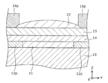
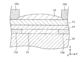
- FIG. 6A is a partial cross-sectional view of solar cell 1 in the manufacturing process according to the present embodiment, taken along line VIa-VIa in FIG. 5B. That is, FIG. 6A is a partial cross-sectional view of a region not irradiated with the laser in the laser processing step.
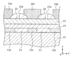
- FIG. 6B is a partial cross-sectional view of solar cell 1 in the manufacturing process according to the present embodiment, taken along line VIb-VIb in FIG. 5B. That is, FIG. 6B is a partial cross-sectional view of the area irradiated with the laser in the laser processing step.
- a groove 22a penetrating to the conductive layer 15 is formed in the resist film 22.
- a groove 22a corresponding to the irradiation range E1 is formed.
- the first separation groove 17 is used to separate the underlayer 14 into the n-side underlayer 14n and the p-side underlayer 14p by etching the back surface 10b where the groove 22a is formed in the resist film 22.
- An under layer removing step of forming the lower layer is performed (S16).
- the conductive layer 15 is partially etched using the resist film 22 as a mask. Thereby, the conductive layer 15 is divided in the separation groove, and the n-side conductive layer 15n and the p-side conductive layer 15p separated from each other are formed.
- the conductive layer 15 can be etched using, for example, a ferric chloride (FeCl 3 ) aqueous solution, hydrochloric acid hydrogen peroxide, or sulfuric acid hydrogen peroxide.
- a part of base layer 14 which is a transparent conductive layer is exposed by this process.
- the exposed underlayer 14 is etched using the resist film 22 and the conductive layer 15 separated in the separation groove as a mask.
- the underlayer 14 is separated in the first separation groove 17, and the n-side underlayer 14n and the p-side underlayer 14p (see FIG. 7B described later) separated from each other are formed.
- the underlayer 14 can be etched using, for example, a hydrogen chloride (HCl) aqueous solution or an oxalic acid aqueous solution.
- FIG. 7A is a partial cross-sectional view of the solar battery cell 1 according to the present embodiment after the underlayer removal step, at a position corresponding to the line VIa-VIa in FIG. 5B. That is, FIG. 7A is a partial cross-sectional view of a region not irradiated with the laser in the laser processing step.
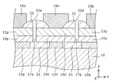
- FIG. 7B is a partial cross-sectional view of the solar battery cell 1 according to the present embodiment after the underlayer removal step, at a position corresponding to the VIb-VIb line in FIG. 5B. That is, FIG. 7B is a partial cross-sectional view of the region irradiated with the laser in the laser processing step.
- the conductive layer 15 and the base layer 14 are not etched. That is, the conductive layer 15 and the base layer 14 remain in the state formed in steps S11 and S12.
- a separation groove penetrating to the conductive layer 15 and the base layer 14 is formed at a position corresponding to the groove 22a of the resist film 22.
- the n-side conductive layer 15n and the p-side conductive layer 15p separated from each other by the separation groove are formed.
- the base layer 14 the n-side base layer 14n and the p-side base layer 14p separated from each other by the separation groove are formed.
- the portion separating the n-side underlayer 14n and the p-side underlayer 14p is the first separation trench 17 (in FIG. 7B, the first separation portion). Describe as 17a). That is, the first separation groove 17 is a groove that separates the n-side underlayer 14 n and the p-side underlayer 14 p.
- the resist removing step (S17) of removing the resist film 22 after the base layer removing step, and the conductive layer removing step of removing part of the n-side conductive layer 15n and the p-side conductive layer 15p (S17) S18) is performed.
- the resist film 22 is removed by an alkaline solution such as NaOH or KOH. Then, in the conductive layer removal step, etching can be performed using a ferric chloride (FeCl 3 ) aqueous solution, hydrochloric acid hydrogen peroxide, and sulfuric acid hydrogen peroxide.
- FeCl 3 ferric chloride
- FIG. 8 is a partial cross-sectional view of the solar battery cell 1 according to the present embodiment after the conductive layer removing step.
- (a) of FIG. 8 is a partial cross-sectional view of the solar battery cell 1 according to the present embodiment after the conductive layer removing step, at a position corresponding to the VIa-VIa line of FIG. 5B. That is, FIG. 8A is a partial cross-sectional view of a region not irradiated with the laser in the laser processing step.
- (B) of FIG. 8 is a partial cross-sectional view of the solar battery cell 1 according to the present embodiment after the conductive layer removing step, at a position corresponding to the VIb-VIb line of FIG. 5B. That is, FIG. 8B is a partial cross-sectional view of the region irradiated with the laser in the laser processing step.
- the underlayer 14 is not etched in the region where the resist film 22 is not irradiated with the laser.
- the underlayer 14 is composed of an n-side underlayer 14 n, a p-side underlayer 14 p, and a first bridge portion 18.
- the first bridge portion 18 is disposed between the n-side underlayer 14n and the p-side underlayer 14p, and connects the n-side underlayer 14n and the p-side underlayer 14p.
- the first bridge portion 18 is formed at the position where the laser is stopped at the position where the scanning path R1 and the scanning paths R2 and R3 intersect in the laser processing step.
- the position is, for example, a region not included in the irradiation ranges E1 to E3 and included in a region between the irradiation range E1 and the irradiation ranges E2 and E3.
- the underlayer 14 is etched and separated by the first separation portion 17a.
- the width L3 (length in the Y-axis direction) of the first bridge portion 18 is substantially equal to the width of the first separation portion 17a.
- the width L 3 of the first bridge portion 18 is smaller than the width of the second separation groove 23.
- the width of the second separation groove 23 is 100 ⁇ m to 200 ⁇ m, and the width L3 of the first bridge portion 18 is 30 ⁇ m.
- the width L3 of the first bridge portion 18 may be approximately equal to the diameter of the laser dot.
- the manufacturing method of the photovoltaic cell 1 is not limited above.
- the order of the steps shown in FIG. 3 may be reversed.
- the resist removal process, the conductive layer removal process, and the underlayer removal process may be performed in this order.
- the resist removing step removal is performed on the resist film 22 in a state in which the groove 22a shown in FIG. 6B is not formed (that is, the resist film 22 in a state formed in the resist film applying step).
- the conductive layer removal step removal of the conductive layer 15 is performed using the n-side electrode 16 n and the p-side electrode 16 p as a mask.
- the n-side conductive layer 15n and the p-side conductive layer 15p are formed.
- laser processing is performed on the exposed base layer 14 to form a first separation groove 17. That is, in the laser processing, the n-side underlayer 14n, the p-side underlayer 14p, and the first bridge portion 18 are formed. Also in this case, as shown in FIG. 5B, the start and stop of the output of the laser are controlled so that the laser is not irradiated twice at the same position. Thereby, the photovoltaic cell 1 shown to (a) and (b) of FIG. 1 is obtained.
- the solar battery cell 1 is a back surface contact type solar battery cell, and is a semiconductor having the light receiving surface 10a on which light is incident and the back surface 10b opposite to the light receiving surface 10a.
- An n-type semiconductor layer 13n and a p-type semiconductor layer 12p provided on the substrate 10 and the back surface 10b of the semiconductor substrate 10 so as to extend in a first direction and to be adjacent to each other in a second direction intersecting the first direction.
- an underlayer 14 provided on the n-type semiconductor layer 13 n and the p-type semiconductor layer 12 p.
- the underlayer 14 is separated from each other by a first separation groove 17 having a first separation portion 17a and a second separation portion 17b extending in mutually different directions, and is provided below the n-type on the n-type semiconductor layer 13n.
- the side underlayer 14n has a first n-side underlayer 141n extending in the first direction, and the p-side underlayer 14p extends in the first direction so as to be adjacent to the first n-side underlayer 141n.
- the first bridge portion 18 includes the first end portion on one side in the first direction of the first n-side base portion 141 n and the p-side base layer 14 p. And the other side of the first p-side base portion 141p in the first direction. In at least one of a boundary between the second end and the n-side underlayer 14n, it separates a first separation unit 17a and a second separation unit 17b.
- the output of the laser may be stopped at the position corresponding to the first bridge portion 18. It can. That is, it is possible to suppress the intersection of the first separation portion 17a and the second separation portion 17b. Therefore, since it can suppress that a laser is irradiated twice to the same position, when the process by a laser is performed, the photovoltaic cell 1 by which the damage to a semiconductor layer etc. was suppressed can be implement
- the n-side underlayer 14n has a second n-side underlayer 142n extending in the second direction and connecting the other end of the first n-side underlayer 141n in the first direction
- the p-side underlayer 14p has a second p-side underlayer 142p extending in the second direction and connecting one end of the first p-side underlayer 141p in the first direction.
- the first separation portion 17 a extends in the first direction in plan view of the solar battery cell 1 and is provided between the adjacent first n-side base portion 141 n and the first p-side base portion 141 p.
- the second separation portion 17b is provided between the first end and the second p-side base portion 142p, and between the second end and the second n-side base portion 142n, respectively.
- the length in the second direction of the second separation portion 17b is longer than the distance L2 between the adjacent first separation portions 17a.
- the first bridge portion 18 separates the end of the first separating portion 17 a in the first direction from the second separating portion 17 b.
- the first separation groove 17 is formed by scanning the laser multiple times, it is possible to suppress the laser from being irradiated twice to the same position, so that processing by the laser is performed.
- the solar battery cell 1 in which the damage to the semiconductor layer and the like is suppressed can be realized.
- the length L1 of the first bridge portion 18 is equal to or less than the length in the Y axis direction of the first bridge portion 18 (in the present embodiment, the width L3).
- the resistance of the first bridge portion 18 can be increased, so that the influence on the collection of carriers by the first bridge portion 18 is suppressed, and when the processing by the laser is performed, the semiconductor layer etc. It is possible to realize the solar battery cell 1 in which the damage to the device is suppressed.
- the method of manufacturing a solar cell is a method of manufacturing a back surface contact type solar cell, and the light receiving surface 10a on which light is incident, and the light receiving surface 10a
- the laser processing step by stopping the output of the laser at a position where the scanning paths R1 to R3 scanned the laser intersect, the first separation portion 17a and the second separation portion extending in different directions at the position A first separation groove 17 separated from 17b is formed.
- the resist film 22 is removed by laser, the removed conductive layer 15 and underlayer 14 adhere to the periphery thereof as compared with the case where the conductive layer 15 and underlayer 14 are removed directly by laser. Can be suppressed.
- FIG. 9 is a plan view showing a solar battery cell according to this modification. Specifically, FIG. 9 shows an area corresponding to (b) of FIG. 1 in the solar battery cell.
- the underlayer has an n-side underlayer 114 n, a p-side underlayer 114 p, and a first bridge portion 118.
- the underlayer is separated by the first separation groove 117. Specifically, the underlayer is separated into the n-side underlayer 114n and the p-side underlayer 114p by the first separation portion 117a and the second separation portion 117b.
- the first separation portion 117a has a first end bordering the first p-side base portion 141p and the second n-side base portion 142n (see (a) in FIG. 1) in plan view of the solar battery cell. And the other end is provided at the boundary between one of the first n-side base portions 141n adjacent to the first p-side base portion 141p and the second p-side base portion 142p.
- the second separation portion 117b is provided with one end at the boundary between the first p-side base portion 141p and the second n-side base portion 142n in plan view of the solar battery cell, and the other end is It is provided at the boundary between the other of the first n-side base portion 141 n adjacent to the first p-side base portion 141 p and the second p-side base portion 142 p.
- the first separation portion 117a and the second separation portion 117b each have, for example, a curved shape on the end side.
- the first bridge portion 118 is disposed between adjacent ends of the first separation portion 117a and the second separation portion 117b. That is, the first bridge portion 118 separates the first separating portion 117a and the second separating portion 117b extending in different directions at the boundary between the n-side underlayer 114n and the p-side underlayer 114p.
- FIG. 3 The present modification is characterized in the laser processing step shown in FIG. 3 and only the laser processing step will be described. The other steps are the same as in the first embodiment.
- FIG. 10 is a plan view showing the scanning path of the laser in the laser processing step according to the present modification. Specifically, FIG. 10 shows a region corresponding to the dashed region A shown in FIG.
- scanning is performed along a scanning path R11, and a laser is irradiated.
- the resist film 22 in the range of the irradiation range E11 is irradiated with a laser. That is, in the present modification, the groove can be formed in the resist film 22 by one scanning.
- the irradiation range E11 indicates the range in which the laser is irradiated in the scanning path R11.
- the scanning path R11 has a shape that is at least partially curved. That is, in the region between the n-side electrode 16n and the p-side electrode 16p, the scanning path R11 has a curved path.
- the laser is turned on at a curved and scanning position P11. Then, the laser is irradiated to the position P12. That is, the output of the laser is turned off before passing the position where the scanning path R11 crosses. Then, the scanning path R11 is scanned in a state where the output of the laser is stopped, and the output of the laser is turned on at a position P13 which has passed the position where the scanning path R11 intersects. That is, the laser irradiation is not performed at the position where the scanning path R11 intersects. That is, the laser is not irradiated twice at the same position. Then, the laser irradiation is performed until the position P14 is reached, and the output of the laser is stopped at the position P14.
- the output of the laser is stopped at the position where the scanning path R11 for scanning the laser intersects, so that the first separation portion 117a and the second separation portion 117b extending in different directions at the position A first separation groove 117 separated by a first bridge portion 118 can be formed. Thereby, the photovoltaic cell 1 shown in FIG. 9 is obtained.
- the n-side underlayer 114n extends in the second direction intersecting the first direction, and in the first direction of the first n-side underlayer 141n.
- the p-side underlayer 114p extends in the second direction and has one side in the first direction of the first p-side underlayer 141p.
- a second p-side base 142p connecting the ends of One end of the first separation portion 117 a is provided at the boundary between the first p-side base portion 141 p and the second n-side base portion 142 n in plan view of the solar battery cell, and the other end is
- the first p-side base portion 141p is provided at the boundary between one of the first n-side base portions 141n adjacent to the first p-side base portion 141p and the second p-side base portion 142p.
- the second separation portion 117b has one end provided at the boundary between the first p-side base portion 141p and the second n-side base portion 142n in plan view of the solar battery cell, and the other end A portion is provided at the boundary between the other of the first n-side base portion 141 n adjacent to the first p-side base portion 141 p and the second p-side base portion 142 p.
- the first bridge portion 118 separates adjacent end portions of the first separation portion 117a and the second separation portion 117b.
- the solar battery cell according to the present modification will be described below with reference to FIGS. 11 to 13.
- the present modification is characterized in the irradiation range to which the laser is irradiated in the laser processing process. That is, the positions at which the first separating portion and the second separating portion are formed are different from those in the first embodiment.
- FIG. 11 is a plan view showing the scanning path of the laser in the laser processing step according to the present modification.
- the laser is irradiated along a substantially central portion between the n-side electrode 16n and the p-side electrode 16p, but in this modification, as shown in FIG. 11, the n-side electrode 16n and the p-side The laser is irradiated along the position between the electrode 16p and one of the n-side electrode 16n and the p-side electrode 16p.
- the laser is irradiated by the scanning paths R21 to R23.
- the scanning path R21 is between the n-side electrode 16n and the p-side electrode 16p and of the n-side electrode 16n and the p-side electrode 16p.
- the position near the n-side electrode 16 n is scanned. Therefore, the irradiation range E21 is formed between the n-side electrode 16n and the p-side electrode 16p and at a position closer to the n-side electrode 16n among the n-side electrode 16n and the p-side electrode 16p.
- the irradiation range E21 is formed between the n-side finger electrode 161n and the p-side finger electrode 161p (see (a) in FIG. 1) and at a position near the n-side finger electrode 161n.
- the scanning path R22 scans a position between the n-side electrode 16n and the p-side electrode 16p and near the n-side electrode 16n. Therefore, the irradiation range E22 is formed between the n-side electrode 16n and the p-side electrode 16p and at a position near the n-side electrode 16n. For example, the irradiation range E22 is formed between the n-side finger electrode 161n and the p-side bus bar electrode 162p (see (a) in FIG. 1) and at a position close to the n-side bus bar electrode 162n.
- the scanning path R23 scans a position between the n-side electrode 16n and the p-side electrode 16p and near the n-side electrode 16n. Therefore, the irradiation range E23 is formed between the n-side electrode 16n and the p-side electrode 16p and at a position near the n-side electrode 16n. For example, the irradiation range E23 is formed between the p-side finger electrode 161p and the n-side bus bar electrode 162n (see (a) in FIG. 1) and at a position close to the n-side bus bar electrode 162n.
- Positions P21 to P24 correspond to the positions P1 to P4 shown in FIG. 5B, respectively. That is, the laser irradiation is started at the positions P21 and P23, and the laser irradiation is stopped at the positions P22 and P24. That is, the irradiation range E21 is formed between the irradiation ranges E22 and E23.
- FIG. 12A is a partial cross-sectional view of the solar battery cell according to the present variation after the laser processing step, taken along line XIIa-XIIa of FIG. 12B is a partial cross-sectional view of the solar battery cell according to the present variation after the laser processing step, taken along line XIIb-XIIb in FIG.
- a groove 122a penetrating to the conductive layer 15 is formed in the resist film 22.
- grooves 122a corresponding to the irradiation range E21 are formed.
- the groove 122a is formed between the position where the thickness of the resist film 22 is maximized and the n-side electrode 16n or the p-side electrode 16p in a cross-sectional view of the solar battery cell.
- the resist film 22 is formed in a semicylindrical shape.
- the position at which the thickness of the resist film 22 reaches the maximum value is a position approximately at the center of the width (length in the Y-axis direction) of the resist film 22.
- the position at which the thickness of the resist film 22 is maximized is a substantially central position between the n-side electrode 16 n and the p-side electrode 16 p. Therefore, the groove 122a is formed at a position close to one of the n-side electrode 16n and the p-side electrode 16p in a cross sectional view of the solar battery cell. In the present embodiment, the groove 122a is formed at a position near the n-side electrode 16n.
- FIG. 13 is a partial cross-sectional view of the solar battery cell according to the present variation after the underlayer removal step.
- FIG. 13 (a) is a partial cross-sectional view taken along line XIIa-XIIa of FIG. 11, after the base layer removing step of the solar battery cell according to the present modification.
- FIG. 13B is a partial cross-sectional view of the XIIb-XIIb line in FIG. 11 after the underlayer removing step of the solar battery cell according to the present modification.
- the underlayer 14 is not etched in the region where the resist film 22 is not irradiated with the laser.
- the underlayer 14 includes an n-side underlayer 214 n, a p-side underlayer 214 p, and a first bridge portion 218.
- the first bridge portion 218 is disposed between the n-side underlayer 214n and the p-side underlayer 214p, and connects the n-side underlayer 214n and the p-side underlayer 214p.
- the base layer 14 is etched and separated by the first separation portion 217 a.
- the first bridge portion 218 and the first separation portion 217 a have the n-side electrode 16 n and the p-side electrode 16 p in a sectional view of the solar battery cell.
- the p-side electrode 16p is formed on the side.
- separation part formed of the irradiation range E22 is formed in the p side electrode 16p side in the cross sectional view of a photovoltaic cell.
- separation part formed of the irradiation range E23 is formed in the n side electrode 16n side in the cross sectional view of a photovoltaic cell.
- a separation groove is formed by the first separation portion 217a and the second separation portion.
- the solar battery cell according to the present modification is provided on the n-side conductive layer 15n, provided on the n-side electrode 16n formed of a plating film, and on the p-side conductive layer 15p, and plating And a p-side electrode 16p formed of a film.
- the first separation groove (for example, the first separation portion 17a) is between the n-side electrode 16n and the p-side electrode 16p in plan view of the solar battery cell, and the n-side electrodes 16n and p It is disposed at a position near one of the electrodes 16p.
- the portion different from the portion where the thickness of the resist film 22 is maximum can be processed by laser, so that the groove 122a can be formed without increasing the laser output. it can. That is, even when the thickness of the resist film 22 is large, it is possible to suppress an increase in damage to the semiconductor layer by increasing the output of the laser. Therefore, in this modification, when processing by laser is performed, a solar battery cell in which damage to a semiconductor layer or the like is suppressed can be realized.
- the position at which the thickness of the resist film 22 is maximized and the n-side electrode 16 n or p in the cross sectional view of the solar cell is scanned between the side electrodes 16p.
- the laser may be scanned at a position near one of the n-side electrode 16 n and the p-side electrode 16 p in a cross-sectional view of the solar battery cell.
- the laser beam can be processed to a portion different from the portion where the thickness of the resist film 22 is maximum, so that the groove 122a can be formed without increasing the laser output. it can. That is, even when the thickness of the resist film 22 is large, it is possible to suppress an increase in damage to the semiconductor layer by increasing the output of the laser. Furthermore, since the portion where the thickness of the resist film 22 is maximum is not processed by the laser, it is possible to suppress the generation of the remaining film of the resist film 22 after the laser processing. Therefore, when the process by a laser is performed, the damage to a semiconductor layer etc. can be suppressed and a solar cell with an improved yield can be realized.
- FIG. 14 is a partial cross-sectional view of the solar battery cell according to the present modification. Specifically, (a) of FIG. 14 is a partial cross-sectional view of the solar battery cell according to the present modification at a position corresponding to the VIa-VIa line of FIG. 5B. (B) of FIG. 14 is a partial cross-sectional view of the solar battery cell according to the present modification at a position corresponding to the VIb-VIb line of FIG. 5B. In the present modification, the conductive layer removing step shown in FIG. 3 is not performed.
- a conductive layer is comprised from the n side conductive layer 315n, the p side conductive layer 315p, and the 2nd bridge part 24.
- the second bridge portion 24 is formed on the first bridge portion 18.
- the second bridge portion 24 is formed, for example, on the first bridge portion 18 shown in (b) of FIG.
- the n-side conductive layer 315 n and the p-side conductive layer are provided at the positions corresponding to the first separation portion 17 a and the second separation portion 17 b shown in FIG. It has separation grooves separated into 315p. That is, the conductive layer has a separation groove consisting of two separation parts extending in different directions.
- the second bridge portion 24 separates the two separation portions.
- a separation groove e.g., the first separation portion 23a of (b) in FIG. 14
- a separation groove for separating the conductive layer into the n-side conductive layer 315n and the p-side conductive layer 315p is an example of a second separation groove. .
- the second bridge portion 24 By arranging the second bridge portion 24 at the above position, the n-type semiconductor layer 13 n and the p-type semiconductor layer 12 p are connected via the second bridge portion 24.
- the second bridge portion 24 is formed.
- the resistance of the second bridge portion 24 is, for example, about the same as the resistance of the first bridge portion 18.
- the resistance of the second bridge portion 24 is 1 k ⁇ / ⁇ or more.
- the sheet resistance of the conductive layer (in the present embodiment, the second bridge portion 24, the n-side conductive layer 315n, and the p-side conductive layer 315p) is 1 k ⁇ / ⁇ or more.
- the size of the second bridge portion 24 in plan view is substantially equal to that of the first bridge portion 18. Therefore, the resistance of the second bridge portion 24 is high, and conduction between the n-side conductive layer 315 n and the p-side conductive layer 315 p can be suppressed.
- a process of increasing the resistance value of the second bridge portion 24 may be performed.
- the heat treatment may be performed in an oxygen atmosphere to increase the resistance.
- the conductive layer is separated into the n-side conductive layer 315 n and the p-side conductive layer 315 p by the first separation part 23 a.
- the width (length in the Y-axis direction) of the first separation portion 23a is, for example, approximately equal to the width of the first separation portion 17a.
- the solar battery cell according to the present modification includes the conductive layer 15 provided on the n-side underlayer 14 n and the p-side underlayer 14 p.
- the conductive layer 15 is separated from each other by the second separation groove (for example, the first separation portion 23a), and the n-side conductive layer 315n provided on the n-side underlayer 14n and the p-side underlayer 14p.
- a second bridge portion 24 provided on the first bridge portion 18 and separating a second separation groove.
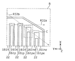
- FIG. 15 is an enlarged view of the vicinity of the short side of the solar battery cell according to the present modification.
- region B in FIG. 15 is an enlarged view of region B in FIG.
- the region B is rotated 180 degrees with respect to FIG. 1 in order to facilitate understanding of the drawing.
- R32a and R32b show the scanning path of a laser.
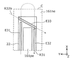
- FIG. 16 is an enlarged view of the area C in FIG. 15, and shows the scanning path of the laser in the area C and the laser irradiation ranges E31, E32, and E33.
- the scanning path of the laser in the vicinity of the short side (near the corner) of the solar battery cell will be described.
- the shape of the solar battery cell is a substantially octagon having long sides and short sides as in this modification, for example, the X coordinate of the tip of the finger electrode 161pe provided at both ends in the Y-axis direction of the solar battery cell. Is different from the X coordinate of the tip of the finger electrode 161p provided at the center in the Y-axis direction. That is, the X coordinate of the tip of finger electrode 161pe is smaller than the X coordinate of the tip of finger electrode 161p.
- the laser scanning is simple.
- the tip of the finger electrode 161p is irradiated with laser in the scanning path R32a to form two finger electrodes 161pe.
- Each tip is separately irradiated with a laser in a scanning path in a direction parallel to the Y axis. That is, three laser scans need to be performed.
- a desired region can be irradiated with a laser by two laser scans of the scanning paths R32a and R32b.
- the two end portions in this modification are a region of several mm to several cm from the outer peripheral portion of the solar cell to the central portion of the solar cell.
- the scanning path R32b is a direction that intersects both the X axis and the Y axis, and is appropriately determined by the X coordinate of each tip of the finger electrode 161pe and the like.
- the scanning path R32 of the laser preferably intersects the finger electrodes 161n on the outer peripheral side of the scanning path R31.
- the resist film 22 in the vicinity of the tip of the finger electrode 161pe preferably has a wider width in the X-axis direction than the resist film 22 in the vicinity of the tip of the finger electrode 161p.
- the scanning path R32b of the laser runs in the direction intersecting the arrangement position of the resist film 22 with both the X axis and the Y axis. That is, the laser irradiation range E33 also extends in the direction intersecting both the X axis and the Y axis.
- the laser irradiation range E33 can be formed without damaging the tip of the finger electrode 161pe.
- the width of the resist film 22 in the X-axis direction may have a width sufficient to form the laser irradiation range E33.
- the finger electrodes 161 p and 161 pe have been described, but the same process may be performed on the finger electrodes 161 n. That is, laser irradiation may be performed in the same scanning path of the laser as described above at the tips of finger electrodes 161ne (not shown) provided at both ends in the Y-axis direction of the solar battery cell.
- the solar battery cell is described as being substantially octagonal, but the form of the solar battery cell is not limited to this.
- finger electrodes 161pe and finger electrodes 161p provided on both ends in the Y-axis direction of the solar battery cell are described separately.
- such an electrode arrangement may not necessarily be provided at both ends of the solar battery cell.
- this modification is applicable even if the portion to deform the pattern is at the center of the solar cell in the Y-axis direction.
- the present modification is applicable not only to the back surface contact type solar battery cell but also to the double side light receiving type solar battery as long as a similar manufacturing process is used.
- the i-type semiconductor layer 12i and the p-type semiconductor layer 12p are stacked and then the i-type semiconductor layer 13i and the n-type semiconductor layer 13n are stacked.
- the layer 13i and the n-type semiconductor layer 13n may be stacked first.
- the order of each process in the manufacturing method of the photovoltaic cell demonstrated by the said embodiment and modification is an example, and is not limited to this. In addition, a part of each step may not be performed.
- each process in the manufacturing method of the photovoltaic cell demonstrated by the said embodiment and modification may be implemented by one process, and may be implemented by a separate process.
- to be performed in one step means that each step is performed using one device, each step is performed sequentially, or that each step is performed in the same place. It is. Also, separate steps may be performed using different devices, each step may be performed at different times (eg, different days), or each step may be performed at different places. It is an intention to include.
Landscapes
- Photovoltaic Devices (AREA)
- Life Sciences & Earth Sciences (AREA)
- Sustainable Development (AREA)
- Engineering & Computer Science (AREA)
- Sustainable Energy (AREA)
- Electrodes Of Semiconductors (AREA)
Abstract
L'invention concerne une cellule solaire (1) comprenant : un substrat semi-conducteur (10) ayant une surface de réception de lumière (10a) et une surface inverse (10b) ; une couche semi-conductrice de type n (13n) et une couche semi-conductrice de type p (12p) disposées sur la surface inverse (10b) du substrat semi-conducteur (10) de façon à s'étendre dans une première direction et de façon à être adjacentes l'une à l'autre dans une seconde direction croisant la première direction ; et une couche de base (14) disposée sur la couche semi-conductrice de type n (13n) et la couche semi-conductrice de type p (12p). La couche de base (14) comprend : une couche de base côté n (14n) et une couche de base côté p (14p), qui sont divisées l'une de l'autre par une première rainure de division (17) ayant des premières parties de division (17a) et des secondes parties de division (17b) ; et des premières parties de pont (18) séparant les premières parties de division (17a) et les secondes parties de division (17b). Les premières parties de pont (18) séparent les premières parties de division (17a) et les secondes parties de division (17b) sur au moins un côté de la delimitation, par rapport à une première direction, entre la couche de base côté n (14n) et la couche de base côté p (14p).
Priority Applications (3)
| Application Number | Priority Date | Filing Date | Title |
|---|---|---|---|
| US16/959,789 US11233164B2 (en) | 2018-01-10 | 2019-01-09 | Solar cell, and method for manufacturing solar cell |
| CN201980007421.8A CN111566821B (zh) | 2018-01-10 | 2019-01-09 | 太阳能单电池和太阳能单电池的制造方法 |
| JP2019564707A JP6936339B2 (ja) | 2018-01-10 | 2019-01-09 | 太陽電池セル、及び、太陽電池セルの製造方法 |
Applications Claiming Priority (2)
| Application Number | Priority Date | Filing Date | Title |
|---|---|---|---|
| JP2018-001923 | 2018-01-10 | ||
| JP2018001923 | 2018-01-10 |
Publications (1)
| Publication Number | Publication Date |
|---|---|
| WO2019139020A1 true WO2019139020A1 (fr) | 2019-07-18 |
Family
ID=67219130
Family Applications (1)
| Application Number | Title | Priority Date | Filing Date |
|---|---|---|---|
| PCT/JP2019/000285 Ceased WO2019139020A1 (fr) | 2018-01-10 | 2019-01-09 | Cellule solaire et procédé de fabrication de cellule solaire |
Country Status (4)
| Country | Link |
|---|---|
| US (1) | US11233164B2 (fr) |
| JP (1) | JP6936339B2 (fr) |
| CN (1) | CN111566821B (fr) |
| WO (1) | WO2019139020A1 (fr) |
Cited By (3)
| Publication number | Priority date | Publication date | Assignee | Title |
|---|---|---|---|---|
| JP2021197507A (ja) * | 2020-06-17 | 2021-12-27 | 株式会社カネカ | 太陽電池の製造方法 |
| JP2023104311A (ja) * | 2022-01-17 | 2023-07-28 | 株式会社カネカ | 太陽電池の製造方法 |
| JP2023111632A (ja) * | 2022-01-31 | 2023-08-10 | 株式会社カネカ | 太陽電池の製造方法および太陽電池 |
Families Citing this family (1)
| Publication number | Priority date | Publication date | Assignee | Title |
|---|---|---|---|---|
| EP4616451A1 (fr) | 2022-11-10 | 2025-09-17 | Meyer Burger (Germany) GmbH | Dispositif photovoltaïque et son procédé de fabrication |
Citations (3)
| Publication number | Priority date | Publication date | Assignee | Title |
|---|---|---|---|---|
| JP2006261447A (ja) * | 2005-03-17 | 2006-09-28 | Toshiba Corp | 半導体装置、及び、半導体装置の製造方法 |
| US20140199806A1 (en) * | 2011-06-30 | 2014-07-17 | Alison Joan Lennon | Dielectric structures in solar cells |
| WO2016157701A1 (fr) * | 2015-03-30 | 2016-10-06 | パナソニックIpマネジメント株式会社 | Cellule de batterie solaire et procédé de fabrication d'une cellule de batterie solaire |
Family Cites Families (3)
| Publication number | Priority date | Publication date | Assignee | Title |
|---|---|---|---|---|
| JP4201457B2 (ja) * | 2000-03-30 | 2008-12-24 | 三洋電機株式会社 | 集積型光起電力装置の製造方法 |
| CN101004457A (zh) * | 2006-01-18 | 2007-07-25 | 精工爱普生株式会社 | 制造具有凹面部分的构件的方法,具有凹面部分的构件,透镜衬底,透射型屏幕和背面投影装置 |
| JP2009088203A (ja) * | 2007-09-28 | 2009-04-23 | Sanyo Electric Co Ltd | 太陽電池、太陽電池モジュール及び太陽電池の製造方法 |
-
2019
- 2019-01-09 JP JP2019564707A patent/JP6936339B2/ja not_active Expired - Fee Related
- 2019-01-09 CN CN201980007421.8A patent/CN111566821B/zh active Active
- 2019-01-09 US US16/959,789 patent/US11233164B2/en active Active
- 2019-01-09 WO PCT/JP2019/000285 patent/WO2019139020A1/fr not_active Ceased
Patent Citations (3)
| Publication number | Priority date | Publication date | Assignee | Title |
|---|---|---|---|---|
| JP2006261447A (ja) * | 2005-03-17 | 2006-09-28 | Toshiba Corp | 半導体装置、及び、半導体装置の製造方法 |
| US20140199806A1 (en) * | 2011-06-30 | 2014-07-17 | Alison Joan Lennon | Dielectric structures in solar cells |
| WO2016157701A1 (fr) * | 2015-03-30 | 2016-10-06 | パナソニックIpマネジメント株式会社 | Cellule de batterie solaire et procédé de fabrication d'une cellule de batterie solaire |
Cited By (6)
| Publication number | Priority date | Publication date | Assignee | Title |
|---|---|---|---|---|
| JP2021197507A (ja) * | 2020-06-17 | 2021-12-27 | 株式会社カネカ | 太陽電池の製造方法 |
| JP7436299B2 (ja) | 2020-06-17 | 2024-02-21 | 株式会社カネカ | 太陽電池の製造方法 |
| JP2023104311A (ja) * | 2022-01-17 | 2023-07-28 | 株式会社カネカ | 太陽電池の製造方法 |
| JP7736581B2 (ja) | 2022-01-17 | 2025-09-09 | 株式会社カネカ | 太陽電池の製造方法 |
| JP2023111632A (ja) * | 2022-01-31 | 2023-08-10 | 株式会社カネカ | 太陽電池の製造方法および太陽電池 |
| JP7826028B2 (ja) | 2022-01-31 | 2026-03-09 | 株式会社カネカ | 太陽電池の製造方法および太陽電池 |
Also Published As
| Publication number | Publication date |
|---|---|
| JPWO2019139020A1 (ja) | 2020-12-10 |
| JP6936339B2 (ja) | 2021-09-15 |
| CN111566821B (zh) | 2023-03-10 |
| US20210159355A1 (en) | 2021-05-27 |
| US11233164B2 (en) | 2022-01-25 |
| CN111566821A (zh) | 2020-08-21 |
Similar Documents
| Publication | Publication Date | Title |
|---|---|---|
| JP5879538B2 (ja) | 光電変換装置及びその製造方法 | |
| JP5820988B2 (ja) | 光電変換装置及びその製造方法 | |
| JP5705968B2 (ja) | 光電変換装置及びその製造方法 | |
| JP5891382B2 (ja) | 光電変換素子の製造方法 | |
| US10134940B2 (en) | Method of manufacturing solar cell | |
| WO2012018119A1 (fr) | Cellule solaire et procédé de fabrication de cellule solaire | |
| US20190207052A1 (en) | Method of manufacturing solar cell, and solar cell | |
| WO2019139020A1 (fr) | Cellule solaire et procédé de fabrication de cellule solaire | |
| JPWO2015040780A1 (ja) | 太陽電池および太陽電池モジュール | |
| WO2018180227A1 (fr) | Cellule solaire | |
| JP6414767B2 (ja) | 太陽電池セル | |
| US20140024168A1 (en) | Method for producing photoelectric conversion device | |
| JP5820989B2 (ja) | 光電変換素子の製造方法 | |
| US10930810B2 (en) | Solar cell and method of manufacturing solar cell | |
| JP6628163B2 (ja) | 太陽電池 | |
| JPWO2012132834A1 (ja) | 太陽電池及び太陽電池の製造方法 | |
| WO2020218000A1 (fr) | Cellule solaire et son procédé de fabrication | |
| WO2012132614A1 (fr) | Dispositif de conversion photoélectrique | |
| WO2019053957A1 (fr) | Cellule solaire, procédé de production de cellule solaire, et module de cellule solaire | |
| WO2012132932A1 (fr) | Cellule solaire et son procédé de fabrication | |
| JP6206843B2 (ja) | 太陽電池 |
Legal Events
| Date | Code | Title | Description |
|---|---|---|---|
| 121 | Ep: the epo has been informed by wipo that ep was designated in this application |
Ref document number: 19739043 Country of ref document: EP Kind code of ref document: A1 |
|
| ENP | Entry into the national phase |
Ref document number: 2019564707 Country of ref document: JP Kind code of ref document: A |
|
| NENP | Non-entry into the national phase |
Ref country code: DE |
|
| 122 | Ep: pct application non-entry in european phase |
Ref document number: 19739043 Country of ref document: EP Kind code of ref document: A1 |