WO2019146268A1 - Élément de stockage et dispositif de stockage - Google Patents
Élément de stockage et dispositif de stockage Download PDFInfo
- Publication number
- WO2019146268A1 WO2019146268A1 PCT/JP2018/044965 JP2018044965W WO2019146268A1 WO 2019146268 A1 WO2019146268 A1 WO 2019146268A1 JP 2018044965 W JP2018044965 W JP 2018044965W WO 2019146268 A1 WO2019146268 A1 WO 2019146268A1
- Authority
- WO
- WIPO (PCT)
- Prior art keywords
- electrode
- voltage
- memory
- storage
- resistance state
- Prior art date
- Legal status (The legal status is an assumption and is not a legal conclusion. Google has not performed a legal analysis and makes no representation as to the accuracy of the status listed.)
- Ceased
Links
Images






Classifications
-
- H—ELECTRICITY
- H10—SEMICONDUCTOR DEVICES; ELECTRIC SOLID-STATE DEVICES NOT OTHERWISE PROVIDED FOR
- H10N—ELECTRIC SOLID-STATE DEVICES NOT OTHERWISE PROVIDED FOR
- H10N70/00—Solid-state devices having no potential barriers, and specially adapted for rectifying, amplifying, oscillating or switching
- H10N70/801—Constructional details of multistable switching devices
- H10N70/881—Switching materials
- H10N70/882—Compounds of sulfur, selenium or tellurium, e.g. chalcogenides
-
- G—PHYSICS
- G11—INFORMATION STORAGE
- G11C—STATIC STORES
- G11C11/00—Digital stores characterised by the use of particular electric or magnetic storage elements; Storage elements therefor
- G11C11/56—Digital stores characterised by the use of particular electric or magnetic storage elements; Storage elements therefor using storage elements with more than two stable states represented by steps, e.g. of voltage, current, phase, frequency
- G11C11/5678—Digital stores characterised by the use of particular electric or magnetic storage elements; Storage elements therefor using storage elements with more than two stable states represented by steps, e.g. of voltage, current, phase, frequency using amorphous/crystalline phase transition storage elements
-
- G—PHYSICS
- G11—INFORMATION STORAGE
- G11C—STATIC STORES
- G11C11/00—Digital stores characterised by the use of particular electric or magnetic storage elements; Storage elements therefor
- G11C11/56—Digital stores characterised by the use of particular electric or magnetic storage elements; Storage elements therefor using storage elements with more than two stable states represented by steps, e.g. of voltage, current, phase, frequency
- G11C11/5685—Digital stores characterised by the use of particular electric or magnetic storage elements; Storage elements therefor using storage elements with more than two stable states represented by steps, e.g. of voltage, current, phase, frequency using storage elements comprising metal oxide memory material, e.g. perovskites
-
- G—PHYSICS
- G11—INFORMATION STORAGE
- G11C—STATIC STORES
- G11C13/00—Digital stores characterised by the use of storage elements not covered by groups G11C11/00, G11C23/00, or G11C25/00
- G11C13/0002—Digital stores characterised by the use of storage elements not covered by groups G11C11/00, G11C23/00, or G11C25/00 using resistive RAM [RRAM] elements
- G11C13/0021—Auxiliary circuits
- G11C13/004—Reading or sensing circuits or methods
-
- H—ELECTRICITY
- H10—SEMICONDUCTOR DEVICES; ELECTRIC SOLID-STATE DEVICES NOT OTHERWISE PROVIDED FOR
- H10B—ELECTRONIC MEMORY DEVICES
- H10B63/00—Resistance change memory devices, e.g. resistive RAM [ReRAM] devices
- H10B63/80—Arrangements comprising multiple bistable or multi-stable switching components of the same type on a plane parallel to the substrate, e.g. cross-point arrays
-
- H—ELECTRICITY
- H10—SEMICONDUCTOR DEVICES; ELECTRIC SOLID-STATE DEVICES NOT OTHERWISE PROVIDED FOR
- H10B—ELECTRONIC MEMORY DEVICES
- H10B63/00—Resistance change memory devices, e.g. resistive RAM [ReRAM] devices
- H10B63/80—Arrangements comprising multiple bistable or multi-stable switching components of the same type on a plane parallel to the substrate, e.g. cross-point arrays
- H10B63/82—Arrangements comprising multiple bistable or multi-stable switching components of the same type on a plane parallel to the substrate, e.g. cross-point arrays the switching components having a common active material layer
-
- H—ELECTRICITY
- H10—SEMICONDUCTOR DEVICES; ELECTRIC SOLID-STATE DEVICES NOT OTHERWISE PROVIDED FOR
- H10B—ELECTRONIC MEMORY DEVICES
- H10B63/00—Resistance change memory devices, e.g. resistive RAM [ReRAM] devices
- H10B63/80—Arrangements comprising multiple bistable or multi-stable switching components of the same type on a plane parallel to the substrate, e.g. cross-point arrays
- H10B63/84—Arrangements comprising multiple bistable or multi-stable switching components of the same type on a plane parallel to the substrate, e.g. cross-point arrays arranged in a direction perpendicular to the substrate, e.g. 3D cell arrays
- H10B63/845—Arrangements comprising multiple bistable or multi-stable switching components of the same type on a plane parallel to the substrate, e.g. cross-point arrays arranged in a direction perpendicular to the substrate, e.g. 3D cell arrays the switching components being connected to a common vertical conductor
-
- H—ELECTRICITY
- H10—SEMICONDUCTOR DEVICES; ELECTRIC SOLID-STATE DEVICES NOT OTHERWISE PROVIDED FOR
- H10D—INORGANIC ELECTRIC SEMICONDUCTOR DEVICES
- H10D84/00—Integrated devices formed in or on semiconductor substrates that comprise only semiconducting layers, e.g. on Si wafers or on GaAs-on-Si wafers
- H10D84/80—Integrated devices formed in or on semiconductor substrates that comprise only semiconducting layers, e.g. on Si wafers or on GaAs-on-Si wafers characterised by the integration of at least one component covered by groups H10D12/00 or H10D30/00, e.g. integration of IGFETs
-
- H—ELECTRICITY
- H10—SEMICONDUCTOR DEVICES; ELECTRIC SOLID-STATE DEVICES NOT OTHERWISE PROVIDED FOR
- H10N—ELECTRIC SOLID-STATE DEVICES NOT OTHERWISE PROVIDED FOR
- H10N70/00—Solid-state devices having no potential barriers, and specially adapted for rectifying, amplifying, oscillating or switching
- H10N70/20—Multistable switching devices, e.g. memristors
-
- H—ELECTRICITY
- H10—SEMICONDUCTOR DEVICES; ELECTRIC SOLID-STATE DEVICES NOT OTHERWISE PROVIDED FOR
- H10N—ELECTRIC SOLID-STATE DEVICES NOT OTHERWISE PROVIDED FOR
- H10N70/00—Solid-state devices having no potential barriers, and specially adapted for rectifying, amplifying, oscillating or switching
- H10N70/801—Constructional details of multistable switching devices
- H10N70/821—Device geometry
- H10N70/823—Device geometry adapted for essentially horizontal current flow, e.g. bridge type devices
-
- H—ELECTRICITY
- H10—SEMICONDUCTOR DEVICES; ELECTRIC SOLID-STATE DEVICES NOT OTHERWISE PROVIDED FOR
- H10N—ELECTRIC SOLID-STATE DEVICES NOT OTHERWISE PROVIDED FOR
- H10N70/00—Solid-state devices having no potential barriers, and specially adapted for rectifying, amplifying, oscillating or switching
- H10N70/801—Constructional details of multistable switching devices
- H10N70/821—Device geometry
- H10N70/826—Device geometry adapted for essentially vertical current flow, e.g. sandwich or pillar type devices
-
- H—ELECTRICITY
- H10—SEMICONDUCTOR DEVICES; ELECTRIC SOLID-STATE DEVICES NOT OTHERWISE PROVIDED FOR
- H10N—ELECTRIC SOLID-STATE DEVICES NOT OTHERWISE PROVIDED FOR
- H10N70/00—Solid-state devices having no potential barriers, and specially adapted for rectifying, amplifying, oscillating or switching
- H10N70/801—Constructional details of multistable switching devices
- H10N70/841—Electrodes
-
- H—ELECTRICITY
- H10—SEMICONDUCTOR DEVICES; ELECTRIC SOLID-STATE DEVICES NOT OTHERWISE PROVIDED FOR
- H10N—ELECTRIC SOLID-STATE DEVICES NOT OTHERWISE PROVIDED FOR
- H10N70/00—Solid-state devices having no potential barriers, and specially adapted for rectifying, amplifying, oscillating or switching
- H10N70/801—Constructional details of multistable switching devices
- H10N70/881—Switching materials
- H10N70/882—Compounds of sulfur, selenium or tellurium, e.g. chalcogenides
- H10N70/8822—Sulfides, e.g. CuS
-
- H—ELECTRICITY
- H10—SEMICONDUCTOR DEVICES; ELECTRIC SOLID-STATE DEVICES NOT OTHERWISE PROVIDED FOR
- H10N—ELECTRIC SOLID-STATE DEVICES NOT OTHERWISE PROVIDED FOR
- H10N70/00—Solid-state devices having no potential barriers, and specially adapted for rectifying, amplifying, oscillating or switching
- H10N70/801—Constructional details of multistable switching devices
- H10N70/881—Switching materials
- H10N70/882—Compounds of sulfur, selenium or tellurium, e.g. chalcogenides
- H10N70/8825—Selenides, e.g. GeSe
-
- H—ELECTRICITY
- H10—SEMICONDUCTOR DEVICES; ELECTRIC SOLID-STATE DEVICES NOT OTHERWISE PROVIDED FOR
- H10N—ELECTRIC SOLID-STATE DEVICES NOT OTHERWISE PROVIDED FOR
- H10N70/00—Solid-state devices having no potential barriers, and specially adapted for rectifying, amplifying, oscillating or switching
- H10N70/801—Constructional details of multistable switching devices
- H10N70/881—Switching materials
- H10N70/882—Compounds of sulfur, selenium or tellurium, e.g. chalcogenides
- H10N70/8828—Tellurides, e.g. GeSbTe
-
- H—ELECTRICITY
- H10—SEMICONDUCTOR DEVICES; ELECTRIC SOLID-STATE DEVICES NOT OTHERWISE PROVIDED FOR
- H10N—ELECTRIC SOLID-STATE DEVICES NOT OTHERWISE PROVIDED FOR
- H10N70/00—Solid-state devices having no potential barriers, and specially adapted for rectifying, amplifying, oscillating or switching
- H10N70/801—Constructional details of multistable switching devices
- H10N70/881—Switching materials
- H10N70/883—Oxides or nitrides
-
- H—ELECTRICITY
- H10—SEMICONDUCTOR DEVICES; ELECTRIC SOLID-STATE DEVICES NOT OTHERWISE PROVIDED FOR
- H10N—ELECTRIC SOLID-STATE DEVICES NOT OTHERWISE PROVIDED FOR
- H10N70/00—Solid-state devices having no potential barriers, and specially adapted for rectifying, amplifying, oscillating or switching
- H10N70/801—Constructional details of multistable switching devices
- H10N70/881—Switching materials
- H10N70/883—Oxides or nitrides
- H10N70/8833—Binary metal oxides, e.g. TaOx
-
- G—PHYSICS
- G11—INFORMATION STORAGE
- G11C—STATIC STORES
- G11C2213/00—Indexing scheme relating to G11C13/00 for features not covered by this group
- G11C2213/70—Resistive array aspects
Definitions
- the present disclosure relates to a memory element having a chalcogenide layer between electrodes and a memory device provided with the same.
- Patent Document 1 discloses a cross point type memory device (memory cell array) in which memory cells are arranged at intersections (cross points) between interconnects.
- the memory cell has a configuration in which a memory element and a switch element for cell selection are stacked, for example, via an intermediate electrode.
- the memory element is provided between a first electrode, a second electrode disposed to face the first electrode, and a first electrode and a second electrode, and further includes tellurium (Te) and selenium.
- a storage layer comprising at least one chalcogen element selected from (Se) and sulfur (S), a transition metal, and oxygen, wherein the storage layer has non-linear resistance and an applied voltage When the threshold voltage is equal to or higher than a predetermined threshold voltage, a low resistance state is obtained, and when the applied voltage is lower than the predetermined threshold voltage, a high resistance state is obtained, thereby providing rectification.
- a storage device includes: one or more first wires extending in one direction; one or more second wires extending in the other direction and intersecting the first wires; A storage element according to an embodiment of the present disclosure, which is disposed at an intersection of a first wiring and a second wiring.
- a storage layer containing a chalcogen element, a transition metal, and oxygen is provided. This makes it possible to realize a memory element having a selection element function.
- the storage layer is formed of at least one chalcogen element selected from tellurium (Te), selenium (Se), and sulfur (S), and a transition metal Since the memory cell is formed using oxygen and oxygen, a selective element function is added to the memory layer. Accordingly, microfabrication is facilitated as compared with a general cross-point type storage device, and therefore, a large capacity can be realized.
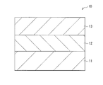
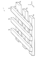
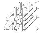
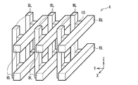
- FIG. 1 is a schematic cross-sectional view showing an example of a configuration of a memory element according to an embodiment of the present disclosure. It is a figure showing an example of a schematic structure of a memory cell array concerning one embodiment of this indication. It is a figure showing an example of a schematic structure of a general memory cell array.
- FIG. 4 is a schematic cross sectional view showing a configuration of a memory cell in the memory cell array shown in FIG. 3.
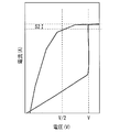
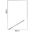
- FIG. 6 is a schematic view for explaining an aspect ratio in the memory cell array shown in FIG. 3; It is a figure showing the write current dependence of the switch operation at the time of the large current writing of the memory element shown in FIG.
- FIG. 3 is a schematic view for explaining an aspect ratio in the memory cell array shown in FIG.
- FIG. 2 It is a figure showing an example of a schematic structure of a memory cell array in a modification of this indication. It is a figure showing the other example of the schematic structure of the memory cell array in the modification of this indication. It is a figure showing the other example of the schematic structure of the memory cell array in the modification of this indication. It is a figure showing the other example of the schematic structure of the memory cell array in the modification of this indication. It is a figure showing the other example of the schematic structure of the memory cell array in the modification of this indication.
- FIG. 10 is a diagram showing an IV characteristic.
- FIG. 1 illustrates an example of a cross-sectional configuration of a memory element (memory element 10) according to an embodiment of the present disclosure.
- the memory element 10 is for selectively operating any of a plurality of memory cells arranged in the memory cell array 1 having a so-called cross point array structure shown in FIG. 2, for example.
- the memory element 10 has a lower electrode 11 (first electrode), a storage layer 12 and an upper electrode 13 (second electrode) in this order.
- the memory layer 12 uses at least one kind of chalcogen element selected from tellurium (Te), selenium (Se) and sulfur (S), a transition metal, and oxygen (O). Have a formed configuration.
- the lower electrode 11 is a wiring material used in a semiconductor process, for example, tungsten (W), tungsten nitride (WN), titanium nitride (TiN), copper (Cu), aluminum (Al), molybdenum (Mo), tantalum (Ta) And tantalum nitride (TaN) and silicide.
- the lower electrode 11 is made of a material that may cause ion conduction due to an electric field such as Cu
- the surface of the lower electrode 11 made of Cu or the like may be W, WN, titanium nitride (TiN), TaN or the like. You may make it coat
- the storage layer 12 switches its resistance state to a low resistance state by applying a voltage equal to or higher than a predetermined voltage between the lower electrode 11 and the upper electrode 13, and the low resistance state is recorded. Also, by applying a predetermined voltage in the reverse direction, the low resistance state is switched to the high resistance state, and the high resistance state is recorded.
- the predetermined voltage is a voltage at which a predetermined write resistance can be obtained, and the storage layer 12 changes the resistance value to be written by changing the magnitude of the applied voltage or current.
- the storage layer 12 of the present embodiment has non-linear resistance and changes to a low resistance state by raising the applied voltage to a predetermined threshold voltage (switching threshold voltage) or more, and the applied voltage is the above threshold voltage.
- the voltage changes to a high resistance state by lowering to a voltage lower than (the switching threshold voltage), and has a rectifying property. That is, the memory element 10 of the present embodiment has a selection element function.
- the memory layer 12 of the present embodiment contains an element of Group 16 of the periodic table, specifically, at least one chalcogen element selected from tellurium (Te), selenium (Se) and sulfur (S). There is.
- Te tellurium
- Se selenium
- S sulfur
- the memory layer 12 contains a transition metal element in addition to the above chalcogen element.
- elements of group 4 of the periodic table titanium (Ti), zirconium (Zr), hafnium (Hf)), elements of group 5 (vanadium (V), niobium (Nb), tantalum (Ta)) and It contains at least one element of group 6 elements (chromium (Cr), molybdenum (Mo), tungsten (W)).
- the storage layer 12 contains oxygen (O).
- the content of oxygen (O) contained in the memory layer 12 is preferably, for example, 55 atomic% or more. At least a part of oxygen (O) in the storage layer 12 is combined with the chalcogen element and the transition metal to form an oxide.
- the memory layer 12 may contain, for example, boron (B), aluminum (Al), gallium (Ga), silicon (Si) and germanium (Ge) in addition to the above elements. Furthermore, the storage layer 12 may contain other elements as long as the effects of the present disclosure are not impaired.
- the thickness (hereinafter simply referred to as thickness) of the storage layer 12 in the stacking direction is preferably, for example, 1 nm or more and 50 nm or less, and more preferably 1 nm or more and 20 nm or less.
- the upper electrode 13 may be a known semiconductor wiring material similarly to the lower electrode 11. However, a stable material which does not react with the storage layer 12 even after the post annealing is preferable.
- the memory element 10 has a memory function and a selection element function. As an example, the characteristic will be described using FIG. 7 described later.
- a voltage higher than a predetermined voltage switching threshold voltage (V1)) is applied to change to the low resistance state (LRS1) and writing is performed.
- V1 switching threshold voltage
- the memory element 10 has a non-linear resistance, so that it returns to the high resistance state (LRS2) although the writing is performed, for example, at a voltage V / 2 bias which is half the write voltage.
- V1 switching threshold voltage
- the read voltage V2 when the read voltage V2 is applied in the high resistance state which is not written or erase operation is performed, it becomes the resistance of HRS1 and the high resistance state and the low resistance state are read by the difference of the current when the read voltage V2 is applied. be able to.
- FIG. 2 is a perspective view of an example of the configuration of the memory cell array 1.
- Memory cell array 1 corresponds to one specific example of the “storage device” of the present disclosure.
- the memory cell array 1 has a so-called cross point array structure. For example, as shown in FIG. 2, one memory cell is provided at each position (cross point) where each word line WL and each bit line BL face each other. It has a cell. That is, the memory cell array 1 includes a plurality of word lines WL, a plurality of bit lines BL, and a plurality of memory cells arranged one by one for each cross point.
- the memory cell is constituted by the memory element 10 described above, and a plurality of memory elements 10 are arranged in a plane (two-dimensional, XY plane direction).
- Each word line WL extends in the same direction as each other.
- the bit lines BL extend in a direction different from the extending direction of the word lines WL (for example, in a direction orthogonal to the extending direction of the word lines WL) and in a direction common to each other.
- the plurality of word lines WL may be arranged in one or more layers, and may be divided into a plurality of layers, for example, as shown in FIG.
- the plurality of bit lines BL are arranged in one or more layers, and may be divided into a plurality of layers, for example, as shown in FIG.
- the memory cell array 1 includes a plurality of memory elements 10 two-dimensionally arranged on a substrate.
- the substrate has, for example, a wiring group electrically connected to each word line WL and each bit line BL, a circuit for connecting the wiring group to an external circuit, and the like.
- Each word line WL and each bit line BL may double as the lower electrode 11 and the upper electrode 13 described above, or may be provided separately from the lower electrode 11 and the upper electrode 13. In that case, for example, the lower electrode 11 is electrically connected to the word line WL, and the upper electrode 13 is electrically connected to the bit line BL.
- a general cross point type memory (memory cell array 100) is, for example, a so-called cross point array in which memory cells (memory cells 110) are arranged at cross points between intersecting wires as shown in FIG. It has a structure. As shown in FIGS. 4 and 5, the memory cell 110 has a configuration in which the selection element 113 is stacked together with the memory element 111, for example, via the intermediate electrode 112. In the cross point array, since the area per unit cell can realize 2F 2 with F as the minimum line width, the cell area can be reduced. Furthermore, the cross point array can realize a large capacity by laminating a plurality of layers in the upper direction (for example, the Z axis direction), for example.
- the thickness of a memory element is about 10 nm to 30 nm.
- the thickness of the selection element is at least 20 nm or more, and the Si diode has a thickness of several hundred nm or more.
- an intermediate electrode having a thickness of at least about 20 nm is provided between the memory layer and the selection element layer for the purpose of preventing mutual diffusion of the respective layers. Therefore, the thickness of the memory cell in a general cross point array is, for example, 50 nm to 100 nm.
- the minimum line width is, for example, 20 nm, as shown in FIG. 5, for example, the aspect ratio of the planar dimension (w) of the total thickness of the memory cell 110 to the height (h1) is 2.5 to 5. .
- the minimum line width is 15 nm, the aspect ratio is increased to 3.3 to 6.7, and the processing of the memory cell becomes difficult.
- a current of several tens to several hundreds of ⁇ A is used as the rewrite current, and the thickness of bit lines and word lines (h2) to prevent disconnection of the wiring.
- the W electrode needs to have a thickness of, for example, about 40 nm. Therefore, when the thickness (h1) of the memory cell 110 and the thickness (h2) of the electrode layer (for example, bit line) are summed (h), the aspect ratio (h / w) at the time of processing is further increased.
- the width is 20 nm
- the aspect ratio is 4.5 to 7
- the processing aspect ratio is increased.
- the need to increase the size of the transistors in the peripheral driver circuit increases the area of the driver circuit, and the array efficiency, which is a ratio of the memory cell array to the memory chip, decreases. Become.
- the storage layer 12 includes at least one chalcogen element selected from tellurium (Te), selenium (Se), and sulfur (S), a transition metal, and oxygen. It was made to use.
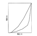
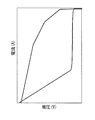
- FIGS. 9 to 11 show the write current dependency of the switch operation of the memory element 111 shown in FIGS.
- FIG. 9 shows the write current dependency of the switch operation at the time of large current writing.
- FIG. 10 shows the write current dependency of the switch operation in the middle current write.
- FIG. 11 shows the write current dependency of the switch operation at the time of small current writing.
- the write current is controlled by current limitation by control of a gate voltage of a transistor or the like. Therefore, in the example of FIG. 10 in which writing is performed with a medium current, when the voltage is swept up to the write voltage, the voltage is rapidly increased at the write voltage threshold (V). When the transistor controls the current flowing at the time of writing and then the voltage is returned to 0 V, the current decreases by drawing a less non-linear IV curve. Therefore, the selection ratio S2, which is the ratio of the current between the write voltage (V) required for the cross point memory and the half selection voltage (2 / V), becomes smaller as shown in FIG.
- control can be performed by the voltage to which the write current is applied.
- the selection ratio S1 which is the ratio of the current between the write voltage (V) necessary for the cross point memory and the half selection voltage (2 / V) can be made large.
- the memory element 10 according to the present embodiment has high non-linearity, it is possible to suppress the leakage current at the half selection and non-selection low.
- the cross point array can be operated without separately using the memory element and the selection element.
- the memory cell can be configured only by the memory element 10.
- FIG. 12 schematically shows a cross sectional configuration of a part of the memory cell array 1.
- the thickness of the memory cell to be processed can be reduced.
- current operation of 1 ⁇ A or less can be performed on the memory cell, so that current flowing to the bit line BL and the word line WL can be suppressed to a low level. Therefore, the thickness of bit line BL and word line WL can be reduced. Therefore, the aspect ratio (h / w) of the memory cell 110 in the memory cell array 100 can be made smaller, thereby facilitating processing of the memory cell and micromachining.
- the transistor of the driver circuit can be reduced. Therefore, the area ratio of the memory cell array occupied in the chip can be increased, and the array efficiency can be improved.
- the memory element 10 in the above embodiment can also constitute a memory cell array having a three-dimensional structure.
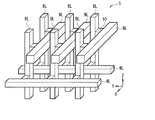
- FIGS. 13 to 16 are perspective views of an example of configurations of memory cell arrays 2 to 5 having a three-dimensional structure according to a modification of the present disclosure.
- each word line WL extends in a common direction.
- the bit lines BL extend in a direction different from the extending direction of the word lines WL (for example, in a direction orthogonal to the extending direction of the word lines WL) and in a direction common to each other.
- the plurality of word lines WL and the plurality of bit lines BL are respectively arranged in a plurality of layers.
- the first layer in which the plurality of word lines WL are arranged and the first layer in which the plurality of word lines WL are arranged are adjacent to each other.
- a plurality of bit lines BL are arranged in a layer between the second layer and the second layer.
- the third layer in which the plurality of bit lines BL are arranged and the third layer in which the plurality of bit lines BL are arranged are adjacent to each other.
- a plurality of word lines WL are arranged in the layer between the fourth layer.
- the plurality of word lines WL and the plurality of bit lines BL are memory cell arrays Are alternately arranged in the stacking direction of.
- the memory cell array of this modification has a vertical cross-point structure in which one of the word line WL or bit line BL is provided parallel to the Z-axis direction and the other is provided parallel to the XY plane direction.
- a plurality of word lines WL extend in the X axis direction
- a plurality of bit lines BL extend in the Z axis direction
- memory elements 10 are arranged at respective cross points. It is also good.
- FIG. 14 even if memory elements 10 are arranged on both sides of the cross points of the plurality of word lines WL and the plurality of bit lines BL extending in the X-axis direction and the Z-axis direction, respectively. Good.
- FIG. 13 shows a vertical cross-point structure in which one of the word line WL or bit line BL is provided parallel to the Z-axis direction and the other is provided parallel to the XY plane direction.
- the plurality of word lines WL and the plurality of bit lines BL do not necessarily extend in one direction.
- the plurality of bit lines BL extend in the Z-axis direction
- the plurality of word lines WL bend in the Y-axis direction while extending in the X-axis direction. It may be bent in the axial direction and stretched in a so-called U shape in the XY plane.
- the memory cell array of the present disclosure has a three-dimensional structure in which the plurality of memory elements 10 are arranged in a plane (two-dimensional, XY plane direction) and further stacked in the Z-axis direction.
- a large capacity storage device can be provided.
- Example 1 First, a plug-like electrode of 160 nm ⁇ made of TiN was formed as a lower electrode, and then the surface was cleaned by reverse sputtering or the like. Subsequently, the Hf target and the Te target were simultaneously discharged by co-sputtering, reactive sputtering was performed using an atmosphere gas in which argon (Ar) and oxygen (O) were mixed at 1: 1, and a storage layer was formed. At this time, the deposition power was adjusted so that the composition ratio of Hf to Te was 4: 6, and (Hf70Te30) Ox was deposited to a thickness of 10 nm. Composition analysis was performed by RBS (Rutherford backscattering), and the composition ratio of oxygen was 55% with respect to the total of the other elements. This is hereinafter referred to as (Hf70Te30) O60.
- Example 1 Example 1 to evaluate its IV characteristics.
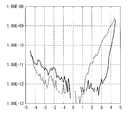
- FIG. 17 shows an IV curve of Experimental Example 1.
- Experimental Example 1 when the write voltage was 4.5 V, writing was possible at 3 nA.
- the on / off selectivity at V / 2 bias was 2.03 digits.
- Example 2 In Experimental Example 2, a memory element was manufactured using the same method as Experimental Example 1 except that the flow rate ratio of Ar / O was set to 1: 2 and the oxygen flow rate ratio was increased when forming the storage layer. .
- the oxygen composition ratio in the storage layer in Experimental Example 2 was 65% as a result of RBS composition analysis.
- Example 3 In Experimental Example 3, a memory element was manufactured using the same method as Experimental Example 1 except that when forming the storage layer, the flow ratio of Ar / O was set to 2: 1 and the oxygen flow ratio was increased. .
- the oxygen composition ratio in the memory layer in Experimental Example 3 was 40% as a result of RBS composition analysis.
- Example 4 In Experimental Example 4, a memory element was manufactured using the same method as Experimental Example 1 except that the film formation rate of Hf / Te was changed by changing the input power ratio at the time of film formation.
- the oxygen composition ratio in the memory layer in Experimental Example 3 was 40% as a result of RBS composition analysis.
- Example 5 In Experimental Example 5, a memory element was manufactured using the same method as Experimental Example 1 except that Zr was used in addition to Hf and Te when forming the storage layer.
- Example 6 In Experimental Example 6, a memory element was manufactured using the same method as Experimental Example 1 except that Al was used in addition to Hf and Te when forming the memory layer.
- Example 7 a memory element was manufactured using the same method as Experimental Example 1 except that B was used in addition to Hf and Te when forming the memory layer.
- the write voltage increased as the composition ratio of oxygen increased.
- the write voltage can be adjusted by increasing or decreasing the film thickness. The larger the film thickness, the larger the write voltage, and the smaller the film thickness, the smaller the write voltage.
- the write current decreased as the oxygen composition ratio increased, even with the same thickness of the memory layer.
- the selection ratio increases as the oxygen content increases, and the oxygen content is as good as two digits when the oxygen content is 55%, and decreases to 1.2 when the oxygen content is 40%.
- the current ratio in the on state and the off state can not be sufficiently obtained in the cross point array due to the influence of the leak current. This makes it difficult to select a memory cell without error, and it is assumed that it becomes difficult to operate a larger memory array. Therefore, it is preferable that the oxygen content of the memory material of the present invention is 55% or more.
- the ratio of Hf to Te could be 50:50 as shown in Experimental Example 4 as well as 70:30 of Experimental Examples 1 to 3. However, in this case, it is found that the ratio of Hf to Te is preferably Hf larger than at least 30:70 because the write current increases and the selectivity decreases.
- FIG. 17 shows that Te is effective as a chalcogen element with respect to the fact that the resistance change of the memory element 10 of the present embodiment exhibits non-linearity. From this, it can be inferred that similar effects can be obtained in Se and S. Therefore, as a material of the memory layer of the memory element of the present disclosure, Se and S other than Te may be contained as a chalcogen element, and it can be said that Se or S may be used instead of Te.
- the method of film formation is not limited to this, and for example, HfO 2 and TeO 2 are alternately stacked using a method such as ALD.
- a storage layer may be formed.
- the film thickness of the memory layer although a sufficiently low write current and off current were obtained at 10 nm in the experimental example, it is preferable to be at least 20 nm or less from the easiness of etching described above.
- the present disclosure can have the following configurations.
- Te tellurium
- Se selenium
- S sulfur
- oxygen oxygen
- the storage layer has non-linear resistance and is in a low resistance state by setting the applied voltage to a predetermined threshold voltage or higher, and in a high resistance state by setting the applied voltage to a voltage lower than the predetermined threshold voltage. Memory element with more rectification.
- the transition metal is titanium (Ti), zirconium (Zr), hafnium (Hf), vanadium (V), niobium (Nb), tantalum (Ta), chromium (Cr), molybdenum (Mo), tungsten (W)
- the storage element according to (1) which is at least one of them.
- the storage layer includes tellurium oxide.
- the storage layer further includes at least one of boron (B), aluminum (Al), gallium (Ga), silicon (Si) and germanium (Ge).
- the storage element according to any one of the above.
- the storage layer switches a resistance state at a predetermined voltage or more and records a low resistance state by applying a voltage between the first electrode and the second electrode, and records a low resistance state, and the reverse of the predetermined voltage.
- the storage element is A first electrode, A second electrode disposed opposite to the first electrode; It is provided between the first electrode and the second electrode, and contains at least one chalcogen element selected from tellurium (Te), selenium (Se) and sulfur (S), a transition metal, and oxygen.
- Te tellurium
- Se selenium
- S sulfur
- the storage layer has non-linear resistance and is in a low resistance state by setting the applied voltage to a predetermined threshold voltage or more, and is set in a high resistance state by setting the applied voltage to a voltage lower than the predetermined threshold voltage.
Landscapes
- Engineering & Computer Science (AREA)
- Chemical & Material Sciences (AREA)
- Computer Hardware Design (AREA)
- Materials Engineering (AREA)
- Crystallography & Structural Chemistry (AREA)
- Semiconductor Memories (AREA)
Abstract
Un élément de stockage selon un mode de réalisation de la présente invention comprend : une première électrode ; une seconde électrode disposée à l'opposé de la première électrode ; et une couche de stockage qui est disposée entre la première électrode et la seconde électrode, et comprend au moins un élément chalcogène sélectionné parmi le tellure (Te), le sélénium (Se) et le soufre (S), un métal de transition et de l'oxygène. La couche de stockage a une résistivité non linéaire et une propriété de redressement de telle sorte qu'un état de faible résistance est obtenu lorsqu'une tension appliquée est supérieure ou égale à une tension de valeur de seuil prédéterminée, et un état de résistance élevée est obtenu lorsque la tension appliquée est une tension inférieure à la tension de valeur de seuil prédéterminée.
Priority Applications (3)
| Application Number | Priority Date | Filing Date | Title |
|---|---|---|---|
| CN201880086971.9A CN111630656B (zh) | 2018-01-25 | 2018-12-06 | 存储元件和存储装置 |
| KR1020207020334A KR102631895B1 (ko) | 2018-01-25 | 2018-12-06 | 기억 소자 및 기억 장치 |
| US16/962,875 US11522132B2 (en) | 2018-01-25 | 2018-12-06 | Storage device and storage unit with a chalcogen element |
Applications Claiming Priority (2)
| Application Number | Priority Date | Filing Date | Title |
|---|---|---|---|
| JP2018-010229 | 2018-01-25 | ||
| JP2018010229A JP2019129239A (ja) | 2018-01-25 | 2018-01-25 | 記憶素子および記憶装置 |
Publications (1)
| Publication Number | Publication Date |
|---|---|
| WO2019146268A1 true WO2019146268A1 (fr) | 2019-08-01 |
Family
ID=67395337
Family Applications (1)
| Application Number | Title | Priority Date | Filing Date |
|---|---|---|---|
| PCT/JP2018/044965 Ceased WO2019146268A1 (fr) | 2018-01-25 | 2018-12-06 | Élément de stockage et dispositif de stockage |
Country Status (5)
| Country | Link |
|---|---|
| US (1) | US11522132B2 (fr) |
| JP (1) | JP2019129239A (fr) |
| KR (1) | KR102631895B1 (fr) |
| CN (1) | CN111630656B (fr) |
| WO (1) | WO2019146268A1 (fr) |
Cited By (1)
| Publication number | Priority date | Publication date | Assignee | Title |
|---|---|---|---|---|
| WO2021054004A1 (fr) * | 2019-09-19 | 2021-03-25 | ソニーセミコンダクタソリューションズ株式会社 | Élément de stockage et dispositif de stockage |
Families Citing this family (4)
| Publication number | Priority date | Publication date | Assignee | Title |
|---|---|---|---|---|
| CN112420919B (zh) * | 2019-08-23 | 2024-06-04 | 联华电子股份有限公司 | 可变电阻式存储器的结构及其制作方法 |
| JP2022139245A (ja) * | 2021-03-11 | 2022-09-26 | キオクシア株式会社 | 記憶装置 |
| WO2023074609A1 (fr) * | 2021-10-27 | 2023-05-04 | 国立研究開発法人産業技術総合研究所 | Matériau amorphe et mémoire de type à points de croisement |
| JP2024044635A (ja) * | 2022-09-21 | 2024-04-02 | キオクシア株式会社 | 記憶装置 |
Citations (3)
| Publication number | Priority date | Publication date | Assignee | Title |
|---|---|---|---|---|
| WO2014103577A1 (fr) * | 2012-12-26 | 2014-07-03 | ソニー株式会社 | Appareil de stockage et procédé de fabrication associé |
| WO2016111724A1 (fr) * | 2015-01-05 | 2016-07-14 | Shih-Yuan Wang | Mémoire vive résistive avec canaux implantés et rayonnés |
| WO2016158429A1 (fr) * | 2015-03-31 | 2016-10-06 | ソニーセミコンダクタソリューションズ株式会社 | Élément de commutation et dispositif de stockage |
Family Cites Families (10)
| Publication number | Priority date | Publication date | Assignee | Title |
|---|---|---|---|---|
| JP2009043905A (ja) * | 2007-08-08 | 2009-02-26 | Hitachi Ltd | 半導体装置 |
| JP4643767B2 (ja) * | 2009-04-15 | 2011-03-02 | パナソニック株式会社 | 抵抗変化型不揮発性記憶装置 |
| JP5708930B2 (ja) * | 2011-06-30 | 2015-04-30 | ソニー株式会社 | 記憶素子およびその製造方法ならびに記憶装置 |
| JP6050015B2 (ja) * | 2012-03-30 | 2016-12-21 | ソニーセミコンダクタソリューションズ株式会社 | 記憶素子および記憶装置 |
| US9761796B2 (en) * | 2012-12-03 | 2017-09-12 | Sony Corporation | Storage device and storage unit with ion source layer and resistance change layer |
| US10418416B2 (en) * | 2012-12-25 | 2019-09-17 | Sony Semiconductor Solutions Corporation | Memory device and memory unit |
| WO2014194069A2 (fr) | 2013-05-29 | 2014-12-04 | Shih-Yuan Wang | Mémoire à accès aléatoire résistive formée sans tension d'écriture |
| US9515262B2 (en) | 2013-05-29 | 2016-12-06 | Shih-Yuan Wang | Resistive random-access memory with implanted and radiated channels |
| FR3019376B1 (fr) * | 2014-03-26 | 2016-04-01 | Commissariat Energie Atomique | Dispositif de memoire vive resistive |
| KR102473660B1 (ko) * | 2016-02-22 | 2022-12-02 | 삼성전자주식회사 | 메모리 소자 및 그 제조 방법 |
-
2018
- 2018-01-25 JP JP2018010229A patent/JP2019129239A/ja active Pending
- 2018-12-06 US US16/962,875 patent/US11522132B2/en active Active
- 2018-12-06 CN CN201880086971.9A patent/CN111630656B/zh active Active
- 2018-12-06 WO PCT/JP2018/044965 patent/WO2019146268A1/fr not_active Ceased
- 2018-12-06 KR KR1020207020334A patent/KR102631895B1/ko active Active
Patent Citations (3)
| Publication number | Priority date | Publication date | Assignee | Title |
|---|---|---|---|---|
| WO2014103577A1 (fr) * | 2012-12-26 | 2014-07-03 | ソニー株式会社 | Appareil de stockage et procédé de fabrication associé |
| WO2016111724A1 (fr) * | 2015-01-05 | 2016-07-14 | Shih-Yuan Wang | Mémoire vive résistive avec canaux implantés et rayonnés |
| WO2016158429A1 (fr) * | 2015-03-31 | 2016-10-06 | ソニーセミコンダクタソリューションズ株式会社 | Élément de commutation et dispositif de stockage |
Cited By (1)
| Publication number | Priority date | Publication date | Assignee | Title |
|---|---|---|---|---|
| WO2021054004A1 (fr) * | 2019-09-19 | 2021-03-25 | ソニーセミコンダクタソリューションズ株式会社 | Élément de stockage et dispositif de stockage |
Also Published As
| Publication number | Publication date |
|---|---|
| US11522132B2 (en) | 2022-12-06 |
| CN111630656B (zh) | 2024-09-03 |
| US20200350498A1 (en) | 2020-11-05 |
| JP2019129239A (ja) | 2019-08-01 |
| KR20200110330A (ko) | 2020-09-23 |
| CN111630656A (zh) | 2020-09-04 |
| KR102631895B1 (ko) | 2024-02-01 |
Similar Documents
| Publication | Publication Date | Title |
|---|---|---|
| KR102507303B1 (ko) | 메모리 소자 | |
| CN102339952B (zh) | 存储元件及其驱动方法以及存储装置 | |
| KR102631895B1 (ko) | 기억 소자 및 기억 장치 | |
| JPWO2019167538A1 (ja) | スイッチ素子および記憶装置ならびにメモリシステム | |
| WO2019198410A1 (fr) | Dispositif de commutation, dispositif de stockage et système de mémoire | |
| WO2016158429A1 (fr) | Élément de commutation et dispositif de stockage | |
| JP2008085071A (ja) | 半導体記憶装置及びその制御方法 | |
| KR20150086182A (ko) | 스위치 소자 및 기억 장치 | |
| US7492635B2 (en) | NOR-type hybrid multi-bit non-volatile memory device and method of operating the same | |
| WO2016129306A1 (fr) | Élément sélectif, cellule de mémoire et dispositif de stockage | |
| US20250194108A1 (en) | Rram process integration scheme and cell structure with reduced masking operations | |
| JPWO2016052097A1 (ja) | スイッチ素子および記憶装置 | |
| US8559210B2 (en) | Memory device | |
| KR102130219B1 (ko) | 비선형 스위치 소자, 이의 제조 방법 및 이를 포함하는 비휘발성 메모리 소자 | |
| KR20230039554A (ko) | 칼코게나이드 기반 물질, 및 이를 포함하는 스위칭 소자 및 메모리 소자 | |
| WO2020261736A1 (fr) | Élément de sélection, cellule de mémoire et dispositif de stockage | |
| CN101359677A (zh) | 相变化存储桥 | |
| CN111668367A (zh) | 存储装置 | |
| US12310031B2 (en) | Multi-layer ovonic threshold switch (OTS) for switching devices and memory devices using the same | |
| US10497437B1 (en) | Decoding scheme for 3D cross-point memory array | |
| CN101281923A (zh) | 具有二极管隔离元件的相变化存储单元 | |
| JP2010278275A (ja) | 半導体記憶装置 | |
| KR20240060306A (ko) | 금속으로 도핑된 스위칭 소자 및 이를 포함하는 반도체 장치 | |
| JP2026052767A (ja) | 記憶装置 |
Legal Events
| Date | Code | Title | Description |
|---|---|---|---|
| 121 | Ep: the epo has been informed by wipo that ep was designated in this application |
Ref document number: 18902573 Country of ref document: EP Kind code of ref document: A1 |
|
| ENP | Entry into the national phase |
Ref document number: 20207020334 Country of ref document: KR Kind code of ref document: A |
|
| NENP | Non-entry into the national phase |
Ref country code: DE |
|
| 122 | Ep: pct application non-entry in european phase |
Ref document number: 18902573 Country of ref document: EP Kind code of ref document: A1 |